Embed Size (px)
Citation preview
ETCHING
E5163 – IC DESIGN
UNIT 2 : INTEGRATED CIRCUIT FABRICATION PROCESS
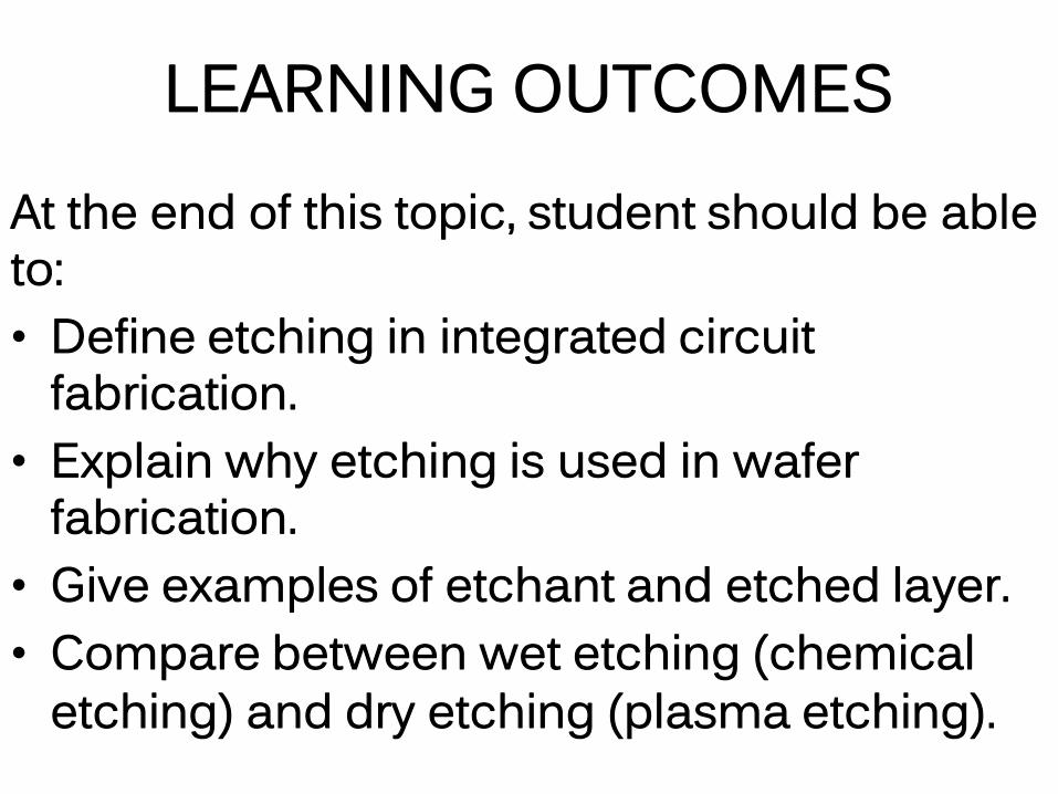
LEARNING OUTCOMESAt the end of this topic, student should be able to:• Define etching in integrated circuit
fabrication.• Explain why etching is used in wafer
fabrication.• Give examples of etchant and etched layer.• Compare between wet etching (chemical
etching) and dry etching (plasma etching).
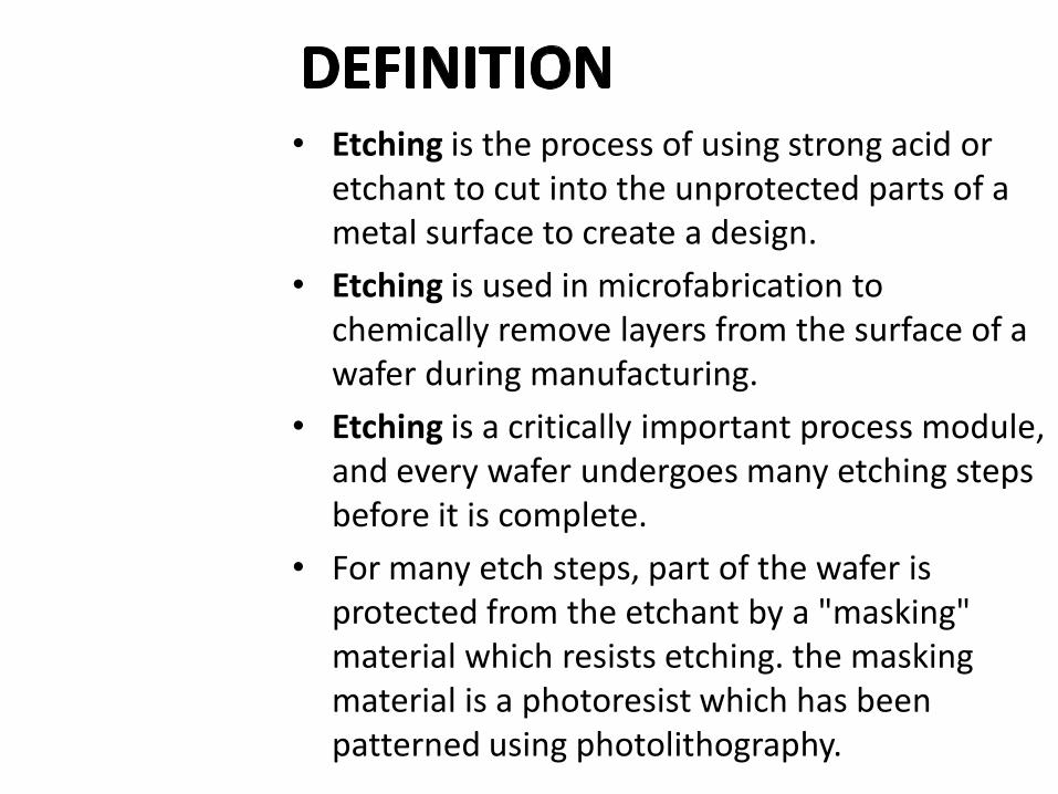
• Etching is the process of using strong acid or etchant to cut into the unprotected parts of a metal surface to create a design.
• Etching is used in microfabrication to chemically remove layers from the surface of a wafer during manufacturing.
• Etching is a critically important process module, and every wafer undergoes many etching steps before it is complete.
• For many etch steps, part of the wafer is protected from the etchant by a "masking" material which resists etching. the masking material is a photoresist which has been patterned using photolithography.
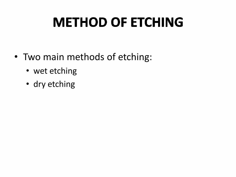
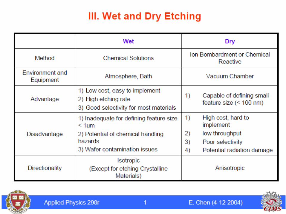
• Two main methods of etching:
• wet etching
• dry etching
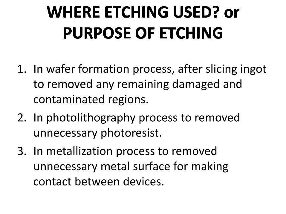
1. In wafer formation process, after slicing ingot to removed any remaining damaged and contaminated regions.
2. In photolithography process to removed unnecessary photoresist.
3. In metallization process to removed unnecessary metal surface for making contact between devices.
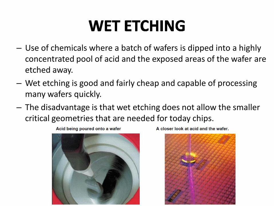
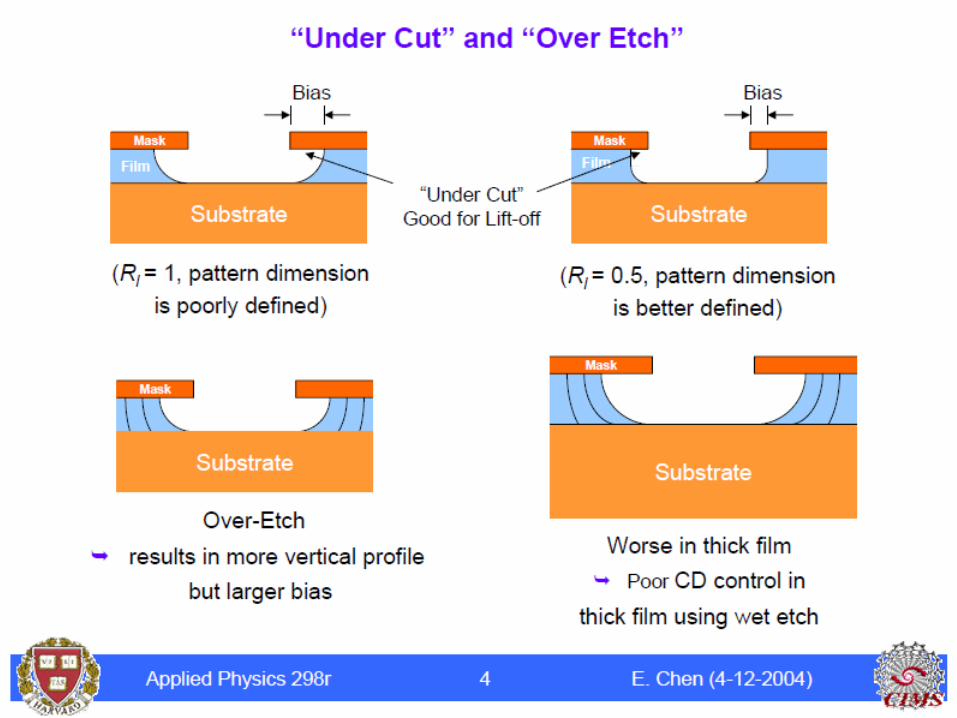
– Use of chemicals where a batch of wafers is dipped into a highly concentrated pool of acid and the exposed areas of the wafer are etched away.
– Wet etching is good and fairly cheap and capable of processing many wafers quickly.
– The disadvantage is that wet etching does not allow the smaller critical geometries that are needed for today chips.
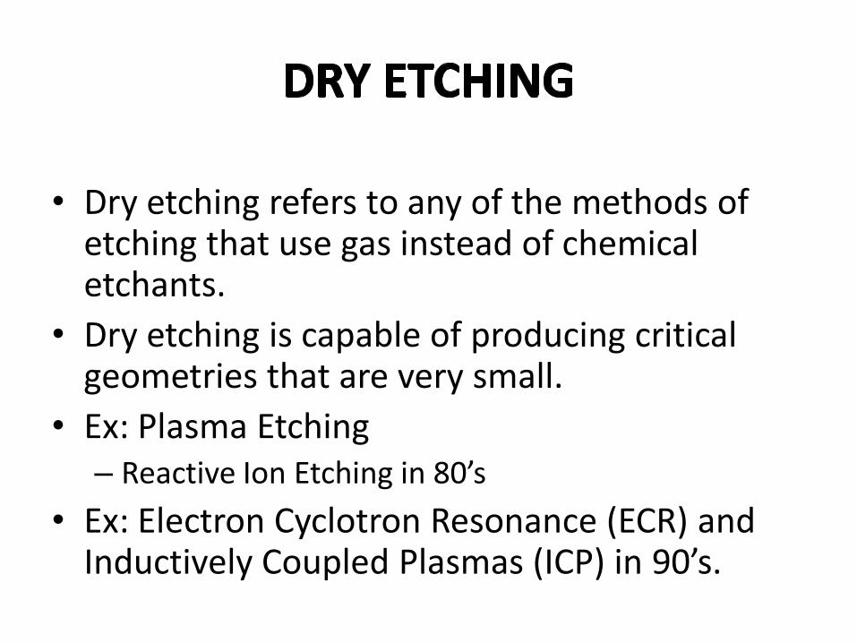
• Dry etching refers to any of the methods of etching that use gas instead of chemical etchants.
• Dry etching is capable of producing critical geometries that are very small.
• Ex: Plasma Etching– Reactive Ion Etching in 80’s
• Ex: Electron Cyclotron Resonance (ECR) and Inductively Coupled Plasmas (ICP) in 90’s.
PLASMA ETCHING
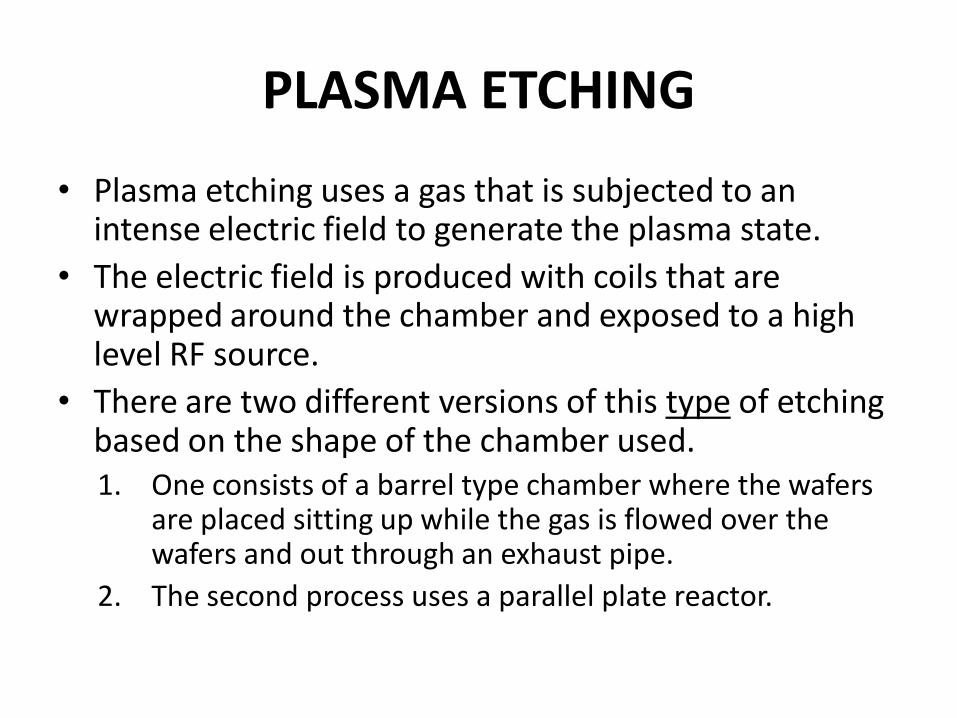
• Plasma etching uses a gas that is subjected to an intense electric field to generate the plasma state.
• The electric field is produced with coils that are wrapped around the chamber and exposed to a high level RF source.
• There are two different versions of this type of etching based on the shape of the chamber used. 1. One consists of a barrel type chamber where the wafers
are placed sitting up while the gas is flowed over the wafers and out through an exhaust pipe.
2. The second process uses a parallel plate reactor.
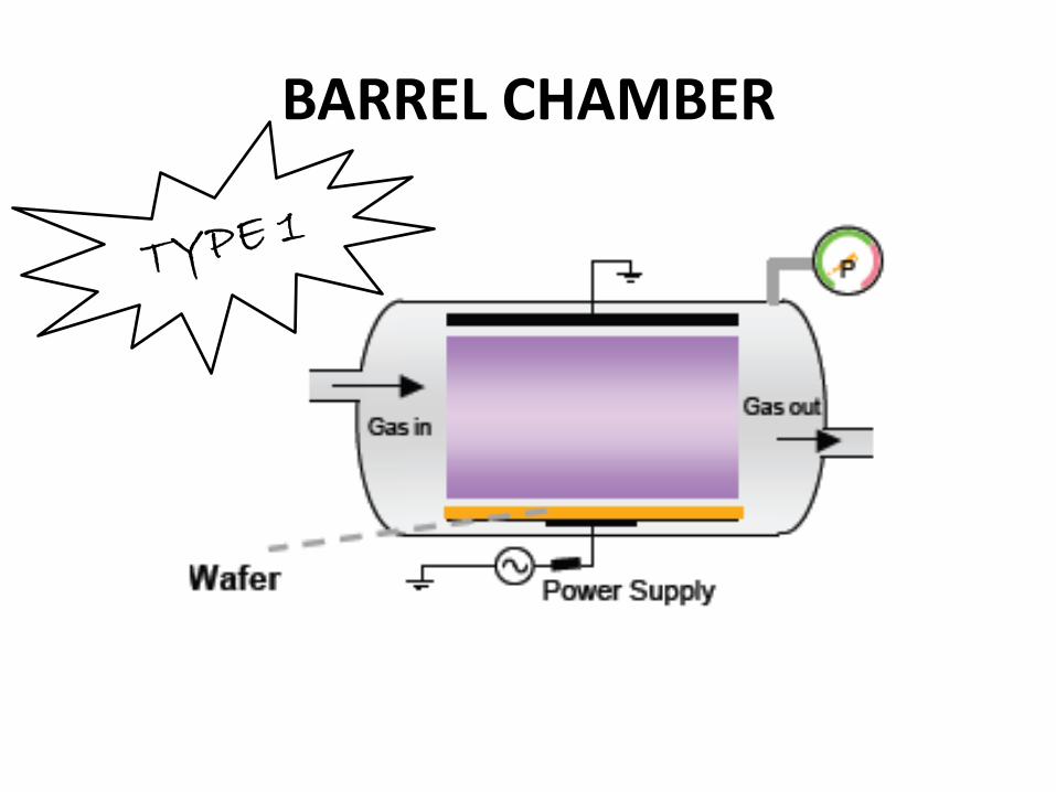
BARREL CHAMBER
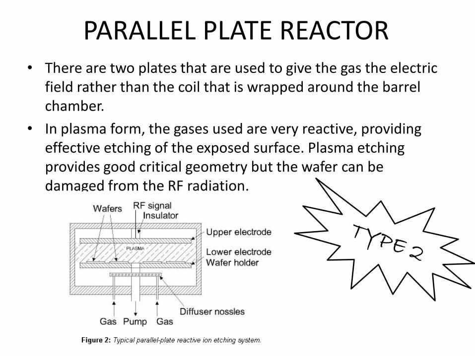
PARALLEL PLATE REACTOR• There are two plates that are used to give the gas the electric
field rather than the coil that is wrapped around the barrel chamber.
• In plasma form, the gases used are very reactive, providing effective etching of the exposed surface. Plasma etching provides good critical geometry but the wafer can be damaged from the RF radiation.
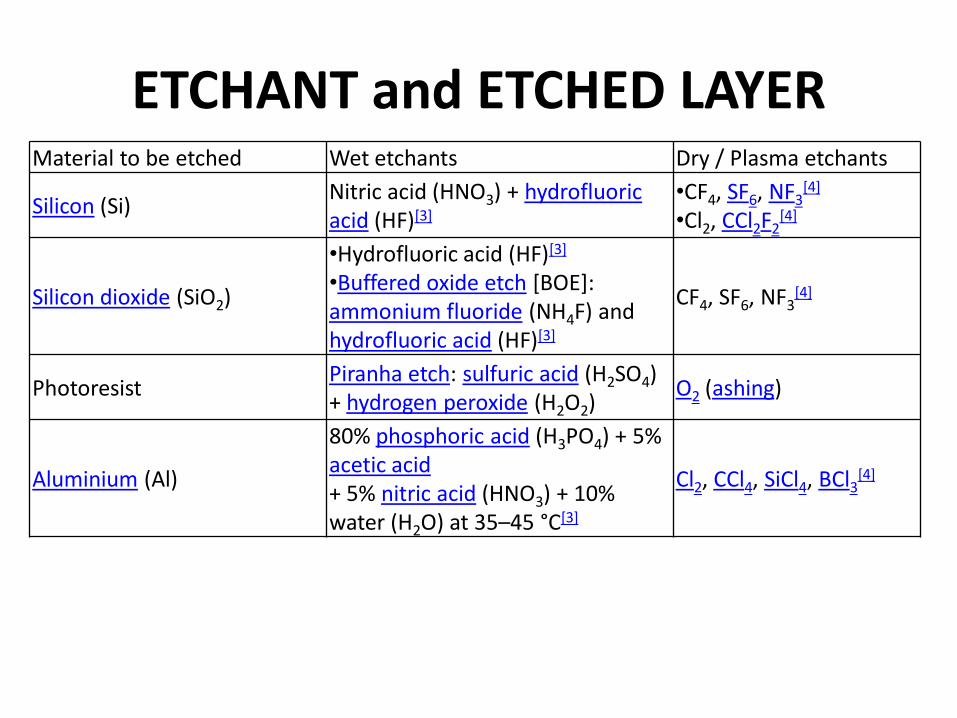
ETCHANT and ETCHED LAYERMaterial to be etched Wet etchants Dry / Plasma etchants
Silicon (Si)Nitric acid (HNO3) + hydrofluoric acid (HF)[3]
•CF4, SF6, NF3[4]
•Cl2, CCl2F2[4]
Silicon dioxide (SiO2)
•Hydrofluoric acid (HF)[3]
•Buffered oxide etch [BOE]: ammonium fluoride (NH4F) and hydrofluoric acid (HF)[3]
CF4, SF6, NF3[4]
PhotoresistPiranha etch: sulfuric acid (H2SO4) + hydrogen peroxide (H2O2)
O2 (ashing)
Aluminium (Al)
80% phosphoric acid (H3PO4) + 5% acetic acid+ 5% nitric acid (HNO3) + 10% water (H2O) at 35–45 °C[3]
Cl2, CCl4, SiCl4, BCl3[4]