Embed Size (px)
Citation preview
Insulator-based Dielectrophoresis for Bacterial
Characterization and Trapping
Diana Nakidde
Thesis submitted to the faculty of the Virginia Polytechnic Institute and State University
in partial fulfillment of the requirements for the degree of
Master of Science
in
Electrical Engineering
Masoud Agah, Chair
Kwang-Jin Koh
Chenming Zhang
February 27th 2015
Blacksburg, VA USA
Keywords: Microelectromechanical Systems (MEMS), Dielectrophoresis (DEP),
Microfabrication, Staphylococcus aureus (S. aureus), Isulator-based Dielectrophoresis
(iDEP)
Copyright 2015, Diana Nakidde
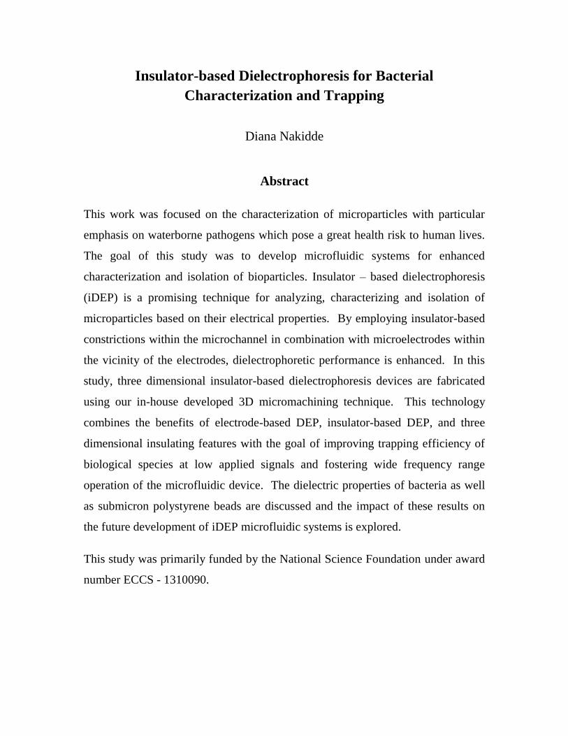
Insulator-based Dielectrophoresis for Bacterial
Characterization and Trapping
Diana Nakidde
Abstract
This work was focused on the characterization of microparticles with particular
emphasis on waterborne pathogens which pose a great health risk to human lives.
The goal of this study was to develop microfluidic systems for enhanced
characterization and isolation of bioparticles. Insulator – based dielectrophoresis
(iDEP) is a promising technique for analyzing, characterizing and isolation of
microparticles based on their electrical properties. By employing insulator-based
constrictions within the microchannel in combination with microelectrodes within
the vicinity of the electrodes, dielectrophoretic performance is enhanced. In this
study, three dimensional insulator-based dielectrophoresis devices are fabricated
using our in-house developed 3D micromachining technique. This technology
combines the benefits of electrode-based DEP, insulator-based DEP, and three
dimensional insulating features with the goal of improving trapping efficiency of
biological species at low applied signals and fostering wide frequency range
operation of the microfluidic device. The dielectric properties of bacteria as well
as submicron polystyrene beads are discussed and the impact of these results on
the future development of iDEP microfluidic systems is explored.
This study was primarily funded by the National Science Foundation under award
number ECCS - 1310090.

| iii
Acknowledgements
First, I would like to thank my advisor, Dr. Masoud Agah, for his invaluable guidance
and support throughout this work. I have learned a great deal from him and grown
immensely both as an individual and as a professional. I’m grateful for the opportunity
he afforded me to learn from him and to work with a brilliant and resilient group of
individuals.
I would like to thank current and former colleagues of the VT MEMS Lab. I would
especially like to thank and acknowledge Dr. Phillip Zellner for his innovative technical
contribution to this work. I’m equally indebted to Mrs. Vaishnavi Srinivasaraghavan for
her boundless well of knowledge and her willingness to share it. Dr. Shree Narayanan,
Mr. Hesam Babahosseini, Ms. Sarah El-Helw, Dr. Hamza Shakeel, Mr. Yahya Hosseini,
Mr. Tyler Shake, Mr. Apoorva Garg, Ms. Deepti Aggarwal, and Ms. Huaning Zhao are
all excellent engineers with bright futures ahead of them, their advice and guidance is
much appreciated.
I would like to thank my family for the love and support. I’m immensely grateful for my
mom, Rose Ssemuju, for believing in me and being a great role model. Her work ethic is
an indispensable lesson I have learned. Special thanks to my dad Thomas More Ssemuju
and my brothers Henry, Joseph, Paul and Michael. I’m heartily thankful for the selfless
contributions of my sister, Liz N. Nangendo, this work would not have been possible
without her.
Lastly, I give glory to my Lord and father!

| iv
Dedicated to My family, and to My Lord and Father
| v
Contents
1.0 Introduction ....................................................................................................................... 1
1.1 Significance and Background ....................................................................................... 1
1.2 Theory ............................................................................................................................. 2
2.0 Three Dimensional Passivated-electrode Insulator-based Dielectrophoresis (3D πDEP) ......... 5
2.1 Introduction ........................................................................................................................... 5
2.2 Theory ................................................................................................................................... 7
2.3 Methods and Materials ........................................................................................................ 10
A. Numerical Device Modeling ........................................................................................... 10
B. Device Fabrication .......................................................................................................... 10
C. Cell Preparation .............................................................................................................. 13
D. Experimental Setup ........................................................................................................ 14
2.4 Results and Discussion ........................................................................................................ 15
A. Numerical Modeling .................................................................................................... 15
B. Frequency Response .................................................................................................... 18
C. Low Voltage Operation ............................................................................................... 19
D. Flow Rate Analysis ...................................................................................................... 21
E. Separation of Particles ................................................................................................ 22
2.5 Discussion and Conclusion.................................................................................................. 24
3.0 Trapping of Submicron Particles using 3D Embedded-electrode Insulator-based
Dielectrophoresis ........................................................................................................................... 27
3.1 Introduction ....................................................................................................................... 27
3.2 Theory................................................................................................................................. 28
3.3 Materials and Methods ..................................................................................................... 29
3.4 Results and Discussion ...................................................................................................... 31
4.0 High Throughput 3D iDEP ...................................................................................................... 32

| vi
4.1 Introduction ....................................................................................................................... 32
4.2 Methods and Materials ..................................................................................................... 32
4.3 Results and discussion ....................................................................................................... 35
4.4 Outlook and Conclusion.................................................................................................... 37
5. Conclusions and Future Work ................................................................................................... 38
5.0 Summary of Results ............................................................................................................ 38
5.1 Pulsed iDEP trapping .......................................................................................................... 38
5.2.1 Introduction ................................................................................................................ 38
5.2.2 Methods and Materials .............................................................................................. 41
5.2.4 Preliminary Results and Discussion .......................................................................... 42
5.2.5 Outlook and Conclusion ............................................................................................. 43
References ..................................................................................................................................... 44
Appendix A: List of Publications .................................................................................................. 47
| vii
Figures
Figure 1.1 Intricate MEMS devices fabricated using MEMS technology. .................................... 2
MEMSnet - www.memsnet.org, Bacteria World - www.bacteria-world.com, AGS Tech -
www.agstech.net, and MEMX - www.memx.com. Used under fair use, 2012 ............ 2
Figure 1.2. a) Particle experiencing positive DEP is drawn to the strongest electric field. b)
Particle experiencing negative DEP is drawn to the weaker field region .................... 3
Figure 2.1: Schematic of 3D πDEP. A. Top view showing reusable electrodes, microfluidic
device and 3D insulating features. B. Isometric view showing material composition.
C. Front view showing the main channel. .................................................................... 6
Figure 2.2: 3D πDEP device fabrication process flow. A. Top view of DRIE lag mask design.
B. Pattern oxide mask and then use RIE lag 3D silicon etch. C. Remove oxide lattice
structure with BOE. D. Anodically bond silicon to Pyrex wafer under vacuum. E.
Melt Pyrex into silicon mold. F. Etch all silicon with KOH. G. Pour PDMS over
Pyrex master and cure. H. Remove PDMS from glass master and punch ports. I.
Plasma bond to glass slide. J. Evaporate electrodes on separate glass substrate. K.
Align electrodes and microfluidic device prior to experimental runs ........................ 11
Figure 2.3: Optical image of 3D πDEP device. (Top) Disposable microfluidic cartridge. (Bottom)
Reusable gold electrodes............................................................................................ 12
Figure 2.4: SEM of a πDEP device comprised of 3D microposts. A. Top view of device. B.
Magnified top view showing 3D posts. C. Cross section of the posts showing the
depth change of the structures. D. Magnified cross section showing constriction .... 13
Figure 2.5: COMSOL simulations of electric fields in 3D πDEP devices. A. Side view of (EE)
profile at 400 Vpp and 300 kHz. B. Top view of (EE) profile at 400 Vpp and 300
kHz. C. Maximum values of (EE) as a function of frequency. D. Simulated values
of the real and imaginary Clausius-Massotti factor ................................................... 16
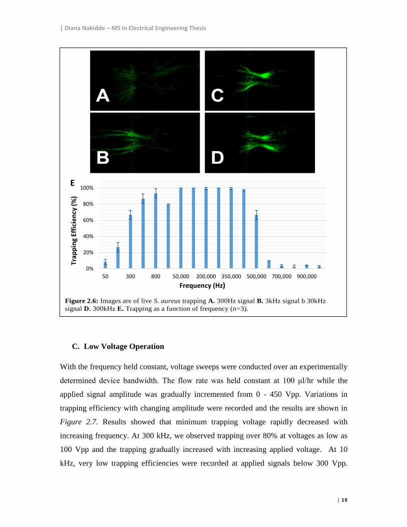
Figure 2.6: Images are of live S. aureus trapping A. 300Hz signal B. 3kHz signal b 30kHz
signal D. 300kHz E. Trapping as a function of frequency (n=3). ...................... 19
Figure 2.7: Low Voltage operation of the 3D DEP device (n=3). A. Poor trapping at 200
Vpp and 800 Hz applied frequency. B. Long pearl chains at low frequency 200
Vpp and 10 kHz. C. Reduced trapping along chains for 200 Vpp and 100 kHz
applied signal. D. Trapping concentrated at the microposts 300 kHz. E.
Trapping efficiency against varied applied signal voltages. ............................... 20
Figure 2.8: Observed DEP trapping of S. aureus by a 3D πDEP device at an applied
electrical signal of 200 Vpp and 300 kHz. Capture efficiency as function of
medium flow rate (n=3). ......................................................................................... 21
| viii
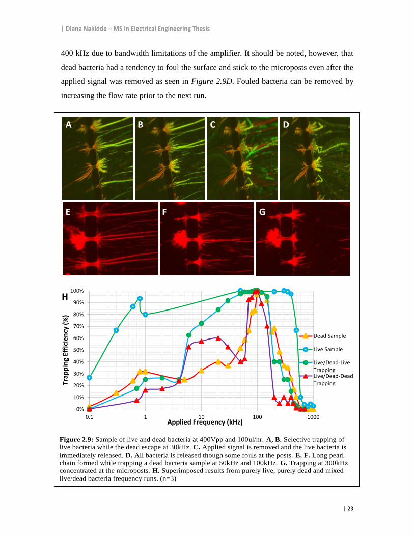
Figure 2.9: Sample of live and dead bacteria at 400Vpp and 100ul/hr. A, B. Selective
trapping of live bacteria while the dead escape at 30kHz. C. Applied signal is
removed and the live bacteria is immediately released. D. All bacteria is
released though some fouls at the posts. E, F. Long pearl chain formed while
trapping a dead bacteria sample at 50kHz and 100kHz. G. Trapping at 300kHz
concentrated at the microposts. H. Superimposed results from purely live,
purely dead and mixed live/dead bacteria frequency runs. (n=3) ...................... 23
Figure 3.1. A-B. Experimental setup C-D. SEM images depicting the 3D insulating micropost
E-F. Images exhibiting trapping and release of submicron beads ............................. 29
Figure 3.2. Sub-micron bead frequency sweep showing trapping efficiency. ............................. 30
Figure 4.1: Proposed high throughput 3D iDEP designs. ..................................................... 33
Figure 4.2. SEM imaging of the round cytometer high throughput 3D iDEP microchannels in
silicon. A. Enhanced imaging of two parallel microchannels. B. A slice image of a
single microchannel C. Half of the microfluidic device showing the inlet ................ 34
Figure 4.3: Images showing high throughput 3D iDEP microfluidic cartridges after
bonding with embedded electrodes. ...................................................................... 35
Figure 4.4. 3D iDEP high throughput device analysis. A. bacteria is infused through the channel.
B. Applied electrical signal is turned on and bacteria is trapped C. Bacteria is
released when the signal is turned off ........................................................................ 37
Figure 5.1. Uniquely responding particles to a pulsed electric signal in an eDEP microfluidic
system ........................................................................................................................ 39
K. Khashayar, et al. Dielectrophoretic platforms for bio-microfluidic systems. Biosensors &
Bioelectronics 26.5 (2011). Used with permission of Elsevier, 2015. ....................... 39
Figure 5.2. Pulsed eDEP trapping of different particle sizes. (a) At f= 2 Hz and V = 12 Vpp,
10µm beads are retained while 3µm and 5µm beads move downstream (b) At f= 1.05
Hz and V = 20 Vpp, 5µm beads are retained, while 3µm and 10µm beads move
downstream (c) At f = 0.3 Hz and V = 20 Vpp, 3µm beads are retained, while both
5µm and 10µm beads move downstream. ↑ indicate stopped particles and → indicate
forward moving particles. .......................................................................................... 40
Cui, Hai-Hang, et al. Separation of particles by pulsed dielectrophoresis. Lab on a Chip 9.16
(2009). Used with permission of the Royal Society of Chemistry, 2015. ................... 40
Figure 5.3. Pulsed iDEP device layout designs ............................................................................ 41
Figure 5.4. Pulsed iDEP device preliminary experimental results ............................................... 42

| ix
Tables
Table 1: Electrical properties of material layers used in the modeling analysis ........................... 17
Table 2: Summary of advantages and disadvantages of 2D iDEP, 2D OπDEP, and 3D πDEP chip
designs. ........................................................................................................................ 25

| Diana Nakidde – MS in Electrical Engineering Thesis
| 1
1.0 Introduction
1.1 Significance and Background
Water is a part of all forms of life, yet many lack access to clean water and are vulnerable
to waterborne bacterial infections. The importance of characterizing and detecting
pathogenic bacteria strains and emerging pathogens cannot be understated. While access
to a treated water supply is the norm in the developed world, access to clean water and
sanitation in the developing world are not the rule and therefore waterborne infections are
rampant.
According to the World Health Organizations, almost 2.5 billion people lack access to an
improved water supply and sanitation. It is estimated that 1.8 billion people use a source
of drinking water that is feacally contaminated [1]. With 2 million annual deaths
attributed to unsafe water, sanitation and hygiene, from these more than 50% are
microbial intestinal infections.
Generally, ingesting water contaminated with human and animal waste is a great
microbial infection risk. Wastewater discharges into coastal and fresh water systems
introduce pathogens into the water system [2]. This holds true in the developed and
developing world. In the USA, it’s been estimated that 560,000 people suffer from
severe waterborne diseases while 7.1 million suffer from some form of mild to moderate
microbial infection leading to an estimated 12,000 deaths a year [3, 4].
Microelectromechanical systems is commonly represented by the acronym MEMS that
was officially adopted by a group of 80 zealots at a Micro Tele-operated Robotics
Workshop in Salt Lake City in 1989 [5]. Microelectromechanical systems refer to
devices with a characteristic length of less than 1000µm but more than 1µm that combine
mechanical and electrical components. Initially MEMS were fabricated using integrated
circuit batch-processing technologies, but lately unique MEMS-specific micromachining
processes are being developed. Figure 1.1 shows some intricate MEMS devices
fabricated using MEMS technology. This multidisciplinary technology is exponentially
progressing at a rate that exceeds our understanding of the physics involved. Some of the
MEMS devices that have been fabricated include actuators, motors, valves, gears,
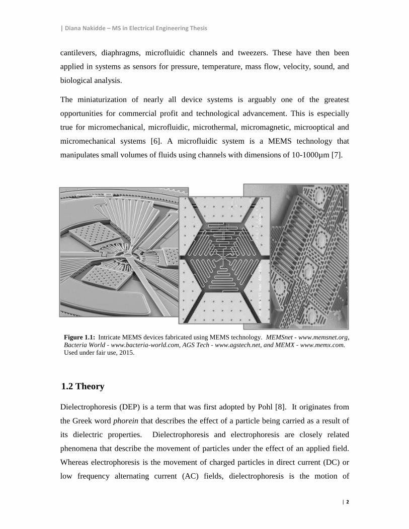
| Diana Nakidde – MS in Electrical Engineering Thesis
| 2
cantilevers, diaphragms, microfluidic channels and tweezers. These have then been
applied in systems as sensors for pressure, temperature, mass flow, velocity, sound, and
biological analysis.
The miniaturization of nearly all device systems is arguably one of the greatest
opportunities for commercial profit and technological advancement. This is especially
true for micromechanical, microfluidic, microthermal, micromagnetic, microoptical and
micromechanical systems [6]. A microfluidic system is a MEMS technology that
manipulates small volumes of fluids using channels with dimensions of 10-1000µm [7].
1.2 Theory
Dielectrophoresis (DEP) is a term that was first adopted by Pohl [8]. It originates from
the Greek word phorein that describes the effect of a particle being carried as a result of
its dielectric properties. Dielectrophoresis and electrophoresis are closely related
phenomena that describe the movement of particles under the effect of an applied field.
Whereas electrophoresis is the movement of charged particles in direct current (DC) or
low frequency alternating current (AC) fields, dielectrophoresis is the motion of
Figure 1.1: Intricate MEMS devices fabricated using MEMS technology. MEMSnet - www.memsnet.org,
Bacteria World - www.bacteria-world.com, AGS Tech - www.agstech.net, and MEMX - www.memx.com.
Used under fair use, 2015.
| Diana Nakidde – MS in Electrical Engineering Thesis
| 3
suspended particles relative to the surrounding medium due to polarizing forces
generated in a non-uniform electric field. Particles are generally <1000 µm in range and
this is mostly because gravity effects prevail in larger particles.
An applied electric field will induce dipole charges within the material of polarizable
particle. For a uniform field, the forces on the dipole charges are equal and opposite and
therefore create a net zero force. In a non-uniform electric field, on the other hand,
opposing forces on the dipole are unequal resulting in a net force on the particle.
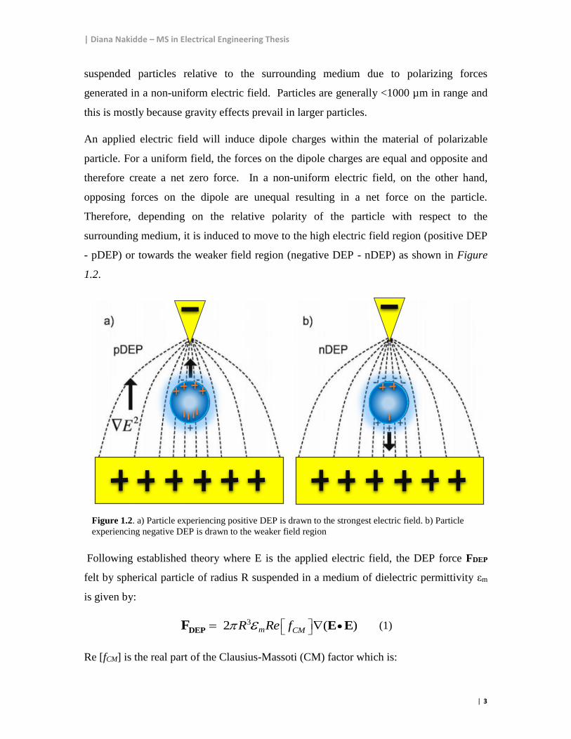
Therefore, depending on the relative polarity of the particle with respect to the
surrounding medium, it is induced to move to the high electric field region (positive DEP
- pDEP) or towards the weaker field region (negative DEP - nDEP) as shown in Figure
1.2.
Following established theory where E is the applied electric field, the DEP force FDEP
felt by spherical particle of radius R suspended in a medium of dielectric permittivity εm
is given by:
3 ( )2 m CMR Re f DEP E EF (1)
Re [fCM] is the real part of the Clausius-Massoti (CM) factor which is:
Figure 1.2. a) Particle experiencing positive DEP is drawn to the strongest electric field. b) Particle
experiencing negative DEP is drawn to the weaker field region
| Diana Nakidde – MS in Electrical Engineering Thesis
| 4
/* * * 2 *p m p mCMf (2)
where εp * and εm * are the complex permittivities of the particle and the medium,
respectively. Complex permittivity is defined as:
* / ( )j (3)
ε and σ are the real permittivity and conductivity while is the angular frequency of the
applied electric field.
Notably, at DC or low frequency AC fields, the DEP separation capability is dominated
by the particle size due to the cubed radius term in Equation 1. Alternatively, at high
frequencies, the DEP separation is mostly influenced by the CM factor because the high
fields are capable of penetrating the cell membrane into the electrically distinct
cytoplasm. The crossover frequency, at which DEP force crosses from nDEP to pDEP or
vice versa, is used to separate different sample populations.
| Diana Nakidde – MS in Electrical Engineering Thesis
| 5
2.0 THREE DIMENSIONAL PASSIVATED-ELECTRODE
INSULATOR-BASED DIELECTROPHORESIS (3D ΠDEP)
Acknowledgement
This work was initiated by Dr. Phillip Zellner during his PhD research. I acknowledge his
innovative technical contribution to this study. I also acknowledge the contributions of
Mohammad Mehdi Alemi, Tyler Shake, Yahya Hosseini, Maria Riquelme, Dr. Amy
Pruden and Dr. Masoud Agah who are co-authors on this manuscript. This manuscript
was recently accepted for publication in Biomicrofluidics Journal [9].
dx.doi.org/10.1063/1.4913497
2.1 Introduction
Dielectrophoresis is a well-known technique for moving, separating and trapping micron
scale particles [10]. It is particularly useful for manipulating biological samples which
usually fall within the micron size range. One of its greatest strengths is the ability to
manipulate several independent variables like signal magnitude, applied frequency, signal
combinations, electrode spacing and microstructure orientation to achieve highly
selective trapping. This technique has been widely used in biological applications to
characterize yeast [11], bacteria [12] and mammalian cells [13].
Electrode based DEP (eDEP) technique is normally used to generate non-uniform
electric fields in the channel [14]. Micro-patterned electrodes in the channel generate
highly localized electric fields and trapping is observed to be concentrated around the
electrodes. Insulator based DEP (iDEP), on the other hand, uses insulating structures
rather than embedded electrodes to generate non-uniform electric field gradients in the
microchannel. iDEP devices have been employed in the past to characterize particles
including bacteria, viruses, cells, and beads [15-17].
Previously, three dimensional insulator-based dielectrophoresis (3D iDEP) devices have
been used to increase sensitivity of iDEP devices. Use of 3D insulating features has been
| Diana Nakidde – MS in Electrical Engineering Thesis
| 6
shown to increase electric field gradient and the DEP force acting on particles. Previous
studies using 3D iDEP technology have been shown to effectively trap bacteria [18].
Earlier work by our group focused on trapping and separation of particles using silicon
DC-Biased iDEP devices [19]. Furthermore, because silicon microfluidic devices were
investigated in comparison to polymer devices, this study demonstrated greatly improved
heat dissipation effects attributed to enhanced thermal dissipation properties of silicon
over polymer substrates.
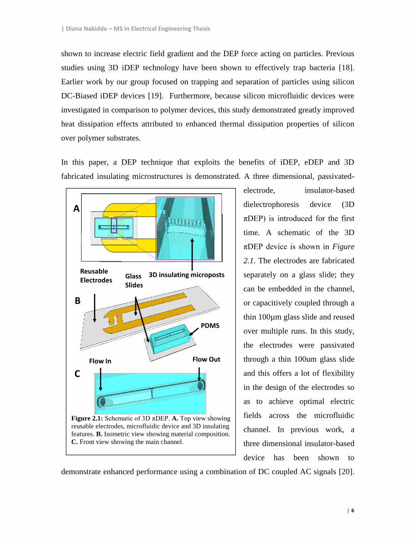
In this paper, a DEP technique that exploits the benefits of iDEP, eDEP and 3D
fabricated insulating microstructures is demonstrated. A three dimensional, passivated-
electrode, insulator-based
dielectrophoresis device (3D
πDEP) is introduced for the first
time. A schematic of the 3D
πDEP device is shown in Figure
2.1. The electrodes are fabricated
separately on a glass slide; they
can be embedded in the channel,
or capacitively coupled through a
thin 100µm glass slide and reused
over multiple runs. In this study,
the electrodes were passivated
through a thin 100um glass slide
and this offers a lot of flexibility
in the design of the electrodes so
as to achieve optimal electric
fields across the microfluidic
channel. In previous work, a
three dimensional insulator-based
device has been shown to
demonstrate enhanced performance using a combination of DC coupled AC signals [20].
Figure 2.1: Schematic of 3D πDEP. A. Top view showing
reusable electrodes, microfluidic device and 3D insulating
features. B. Isometric view showing material composition.
C. Front view showing the main channel.
Flow In Flow Out
Reusable Electrodes
3D insulating microposts
PDMS
Glass Slides
A
B
C
| Diana Nakidde – MS in Electrical Engineering Thesis
| 7
In this previous work demonstrated by our group, the electrodes were in contact with the
medium. This caused the electrodes to be located farther away from the insulating
microstructures responsible for generating electric field gradient. In these iDEP devices,
the voltages are applied across a significant portion of the microchannel increasing the
complexities due to heating effects [21, 22]. In the current study, electrodes are located
within the vicinity of the insulating microposts to minimize heat build-up within the
channel. Reduced electrode spacing minimizes the conductive path travelled by the
current ultimately reducing heat generated within the microchannel. The DEP force is
achieved by 3D insulating structures in the channel. In comparison to traditional iDEP
devices with 2D insulating features, 3D features increase the electric field gradient which
in turn increases the DEP force. 100% trapping efficiency can be achieved at low applied
voltages thus reducing power consumption, the adverse effects of electrothermal flow and
allowing for integration with simpler supporting electronics.
This 3D πDEP is comparable to our previously reported passivated-electrode insulator-
based dielectrophoresis (OπDEP) device [23]. OπDEP combines the benefits of a high
throughput, low cost 2D iDEP and the enhanced sensitivity of eDEP with electrodes
located in the vicinity of the 2D insulating microstructures. A reusable set of electrodes
are activated and the signal capacitively coupled through a thin glass slide into the
microfluidic channel. 3D πDEP, on the other hand, achieves high capture efficiencies at
lower applied voltages and over a wider frequency range. This paper will demonstrate
performance of the 3D πDEP microfluidic device by trapping live and dead
Staphylococcus aureus bacterial cells. Enrichment and separation of this bacterial cell is
especially important because S. aureus is an ubiquitous opportunistic pathogen, whose
infections are becoming increasingly difficult to treat due to the emergence of multiple-
antibiotic resistant strains in recent years.
2.2 Theory
The motion of polarizable particles suspended in a dielectrically dissimilar media when
subjected to a spatially non-uniform electric field is dielectrophoresis (DEP) [24]. Unlike
electrophoresis, particles do not have to possess a net charge to be polarized by DEP
| Diana Nakidde – MS in Electrical Engineering Thesis
| 8
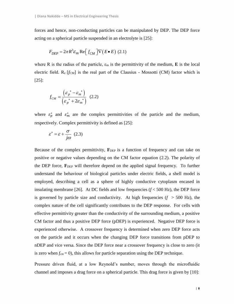
forces and hence, non-conducting particles can be manipulated by DEP. The DEP force
acting on a spherical particle suspended in an electrolyte is [25]:
32 ReDEP CMmF R f E E (2.1)
where R is the radius of the particle, εm is the permittivity of the medium, E is the local
electric field. Re [fCM] is the real part of the Clausius - Mossotti (CM) factor which is
[25]:
2
CM
p m
p m
f
(2.2)
where 𝜀𝑝∗ and 𝜀𝑚
∗ are the complex permittivities of the particle and the medium,
respectively. Complex permittivity is defined as [25]:
j
(2.3)
Because of the complex permittivity, FDEP is a function of frequency and can take on
positive or negative values depending on the CM factor equation (2.2). The polarity of
the DEP force, FDEP will therefore depend on the applied signal frequency. To further
understand the behaviour of biological particles under electric fields, a shell model is
employed, describing a cell as a sphere of highly conductive cytoplasm encased in
insulating membrane [26]. At DC fields and low frequencies (f < 500 Hz), the DEP force
is governed by particle size and conductivity. At high frequencies (f > 500 Hz), the
complex nature of the cell significantly contributes to the DEP response. For cells with
effective permittivity greater than the conductivity of the surrounding medium, a positive
CM factor and thus a positive DEP force (pDEP) is experienced. Negative DEP force is
experienced otherwise. A crossover frequency is determined when zero DEP force acts
on the particle and it occurs when the changing DEP force transitions from pDEP to
nDEP and vice versa. Since the DEP force near a crossover frequency is close to zero (it
is zero when fcm = 0), this allows for particle separation using the DEP technique.
Pressure driven fluid, at a low Reynold’s number, moves through the microfluidic
channel and imposes a drag force on a spherical particle. This drag force is given by [10]:
| Diana Nakidde – MS in Electrical Engineering Thesis
| 9
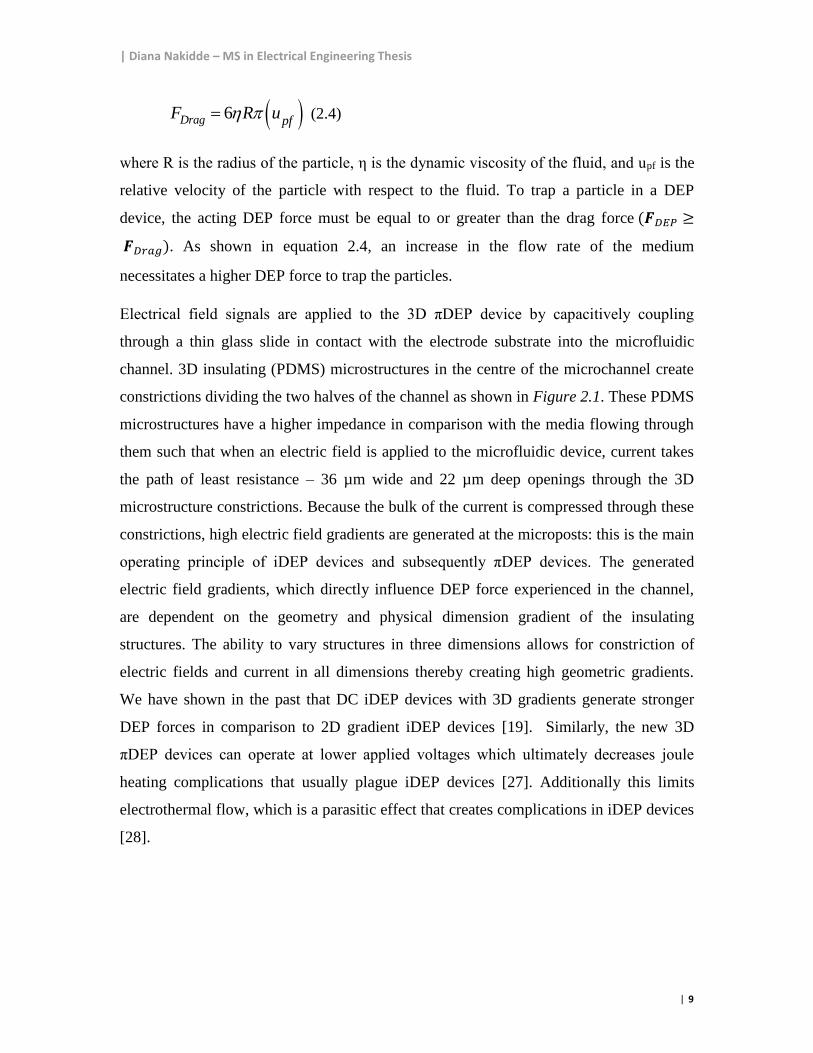
6Drag pfF R u (2.4)
where R is the radius of the particle, η is the dynamic viscosity of the fluid, and upf is the
relative velocity of the particle with respect to the fluid. To trap a particle in a DEP
device, the acting DEP force must be equal to or greater than the drag force (𝑭𝐷𝐸𝑃 ≥
𝑭𝐷𝑟𝑎𝑔). As shown in equation 2.4, an increase in the flow rate of the medium
necessitates a higher DEP force to trap the particles.
Electrical field signals are applied to the 3D πDEP device by capacitively coupling
through a thin glass slide in contact with the electrode substrate into the microfluidic
channel. 3D insulating (PDMS) microstructures in the centre of the microchannel create
constrictions dividing the two halves of the channel as shown in Figure 2.1. These PDMS
microstructures have a higher impedance in comparison with the media flowing through
them such that when an electric field is applied to the microfluidic device, current takes
the path of least resistance – 36 µm wide and 22 µm deep openings through the 3D
microstructure constrictions. Because the bulk of the current is compressed through these
constrictions, high electric field gradients are generated at the microposts: this is the main
operating principle of iDEP devices and subsequently πDEP devices. The generated
electric field gradients, which directly influence DEP force experienced in the channel,
are dependent on the geometry and physical dimension gradient of the insulating
structures. The ability to vary structures in three dimensions allows for constriction of
electric fields and current in all dimensions thereby creating high geometric gradients.
We have shown in the past that DC iDEP devices with 3D gradients generate stronger
DEP forces in comparison to 2D gradient iDEP devices [19]. Similarly, the new 3D
πDEP devices can operate at lower applied voltages which ultimately decreases joule
heating complications that usually plague iDEP devices [27]. Additionally this limits
electrothermal flow, which is a parasitic effect that creates complications in iDEP devices
[28].
| Diana Nakidde – MS in Electrical Engineering Thesis
| 10
2.3 Methods and Materials
A. Numerical Device Modeling
A numerical model of the 3D πDEP devices is created using COMSOL Multiphysics 3.5
(COMSOL Inc., Burlington, MA) under the AC/DC module so as to explore electric field
distributions within the microchannel. A 3D COMSOL model is created for the device
under investigation. The electrical conductivities used for PDMS, glass, air, and
deionized water (DI) are 8.20 × 10⁻¹³ S/m, 1.25 × 10⁻⁹ S/m, 3.00 × 10⁻⁹ S/m, and 8.00 ×
10-4 S/m, respectively. The electrical permittivities used for PDMS, glass, air, and
deionized water are 2.65, 4.65, 1, and 80, respectively. To define boundary conditions,
the electrodes are assigned AC electric potentials while all other boundaries are defined
as electrical insulation. The values for PDMS were set by the manufacturer. The
numerical modelling and simulations are used to evaluate the values of ∇|𝐄|2 as a function
of position in the microchannel and applied frequency signal. This model affirms the
concept in equation 4.1, showing that the DEP force experienced by a given particle in
medium is proportional to ∇|𝐄|2.
B. Device Fabrication
A new process flow for the design and fabrication of the 3D πDEP is implemented in
PDMS as shown in Figure 2.2. Initially a layer of thermal silicon dioxide, 0.4µm thick, is
grown at 1000 °C on a <100> silicon wafer. The oxide layer is used as a mask during the
etch process. Using our 3D silicon micromachining technique [29-31], a photomask
layout consisting of an array of rectangular openings with different sizes and aspect ratios
is created (Figure 2.2A). Thereafter photoresist (S1813) is patterned and the pattern is
transferred to the oxide using an Alcatel AMS-100 Deep Reactive Ion Etcher (DRIE)
with CH4 plasma. The DRIE etch exposes silicon, which is isotropically etched using SF6
plasma (Figure 2.2B). The reactive ion etch lag (RIE lag) and its dependency on the
geometrical patterns of the mask layout is exploited to create 3D cavities and microposts.
This technique provides three dimensional flexibility over structure formation. Next,
photoresist is removed and the silicon substrate is bonded to a Pyrex wafer under vacuum
| Diana Nakidde – MS in Electrical Engineering Thesis
| 11
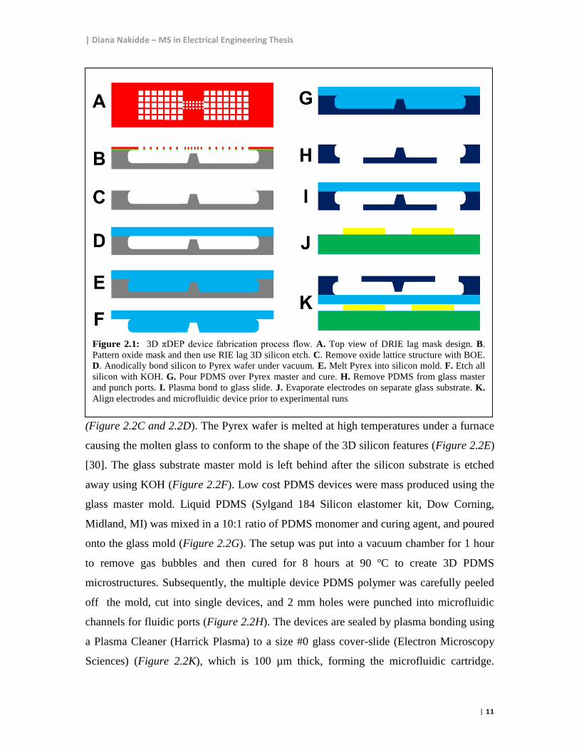
(Figure 2.2C and 2.2D). The Pyrex wafer is melted at high temperatures under a furnace
causing the molten glass to conform to the shape of the 3D silicon features (Figure 2.2E)
[30]. The glass substrate master mold is left behind after the silicon substrate is etched
away using KOH (Figure 2.2F). Low cost PDMS devices were mass produced using the
glass master mold. Liquid PDMS (Sylgand 184 Silicon elastomer kit, Dow Corning,
Midland, MI) was mixed in a 10:1 ratio of PDMS monomer and curing agent, and poured
onto the glass mold (Figure 2.2G). The setup was put into a vacuum chamber for 1 hour
to remove gas bubbles and then cured for 8 hours at 90 ºC to create 3D PDMS
microstructures. Subsequently, the multiple device PDMS polymer was carefully peeled
off the mold, cut into single devices, and 2 mm holes were punched into microfluidic
channels for fluidic ports (Figure 2.2H). The devices are sealed by plasma bonding using
a Plasma Cleaner (Harrick Plasma) to a size #0 glass cover-slide (Electron Microscopy
Sciences) (Figure 2.2K), which is 100 µm thick, forming the microfluidic cartridge.
Figure 2.1: 3D πDEP device fabrication process flow. A. Top view of DRIE lag mask design. B.
Pattern oxide mask and then use RIE lag 3D silicon etch. C. Remove oxide lattice structure with BOE.
D. Anodically bond silicon to Pyrex wafer under vacuum. E. Melt Pyrex into silicon mold. F. Etch all
silicon with KOH. G. Pour PDMS over Pyrex master and cure. H. Remove PDMS from glass master
and punch ports. I. Plasma bond to glass slide. J. Evaporate electrodes on separate glass substrate. K.
Align electrodes and microfluidic device prior to experimental runs
| Diana Nakidde – MS in Electrical Engineering Thesis
| 12
Figure 2.3: Optical image of 3D πDEP device. (Top)
Disposable microfluidic cartridge. (Bottom) Reusable
gold electrodes
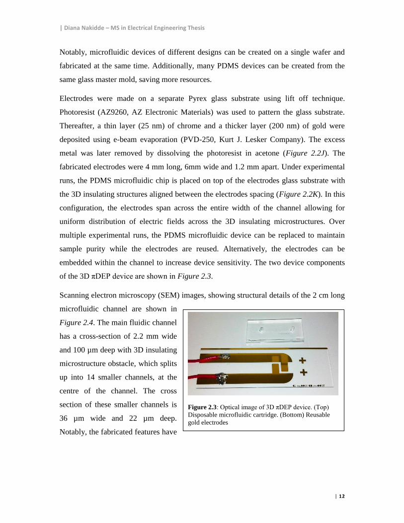
Notably, microfluidic devices of different designs can be created on a single wafer and
fabricated at the same time. Additionally, many PDMS devices can be created from the
same glass master mold, saving more resources.
Electrodes were made on a separate Pyrex glass substrate using lift off technique.
Photoresist (AZ9260, AZ Electronic Materials) was used to pattern the glass substrate.
Thereafter, a thin layer (25 nm) of chrome and a thicker layer (200 nm) of gold were
deposited using e-beam evaporation (PVD-250, Kurt J. Lesker Company). The excess
metal was later removed by dissolving the photoresist in acetone (Figure 2.2J). The
fabricated electrodes were 4 mm long, 6mm wide and 1.2 mm apart. Under experimental
runs, the PDMS microfluidic chip is placed on top of the electrodes glass substrate with
the 3D insulating structures aligned between the electrodes spacing (Figure 2.2K). In this
configuration, the electrodes span across the entire width of the channel allowing for
uniform distribution of electric fields across the 3D insulating microstructures. Over
multiple experimental runs, the PDMS microfluidic device can be replaced to maintain
sample purity while the electrodes are reused. Alternatively, the electrodes can be
embedded within the channel to increase device sensitivity. The two device components
of the 3D πDEP device are shown in Figure 2.3.
Scanning electron microscopy (SEM) images, showing structural details of the 2 cm long
microfluidic channel are shown in
Figure 2.4. The main fluidic channel
has a cross-section of 2.2 mm wide
and 100 µm deep with 3D insulating
microstructure obstacle, which splits
up into 14 smaller channels, at the
centre of the channel. The cross
section of these smaller channels is
36 µm wide and 22 µm deep.
Notably, the fabricated features have
| Diana Nakidde – MS in Electrical Engineering Thesis
| 13
rounded corners acquired by silicon isotropic etching: this is in contrast to sharp edges
typically found in conventional microchannels. Therefore, the 3D aspect accounts for
abrupt changes in cross-sectional area without the limitation of sharp edges.
C. Cell Preparation
Staphylococcus aureus (S. aureus) strain (ATCC 12600) was cultured in brain heart
infusion media (Bactrius Limited, Houston TX). S. aureus cells were cultured in 100 ml
of broth medium at 37 °C and 165 rpm to the exponential growth phase (OD600 ~ 0.8).
Cells were then transferred into two sterile 50 ml centrifuge tubes, and subjected to five
washes by centrifugation (5000 × g for 10 min) and re-suspension in 1× PBS. A
calibration curve relating OD600 to microscopic cell counts was created and used to
quantify the washed bacteria via spectrophotometry thereafter. To express green or red
fluorescence under a microscope, bacteria were stained for 20 minutes using a Live/Dead
viability kit (LIVE/DEAD Backlit, Invitrogen). Prior to experimental runs, S. aureus cells
were centrifuged and re-suspended 5 times in deionized water with a measured
conductivity of 800 µS/m. The deionized water conductivity was measured with a
Figure 2.4: SEM of a πDEP device comprised of 3D microposts. A. Top view of device. B. Magnified
top view showing 3D posts. C. Cross section of the posts showing the depth change of the structures.
D. Magnified cross section showing constriction
| Diana Nakidde – MS in Electrical Engineering Thesis
| 14
solution conductivity meter (SG7, Mettler Toledo, Scherzenbach, Switzerland). The
average cell concentration for experiments was 109 cells/ml.
D. Experimental Setup
An AC signal of 200V peak to peak (Vpp) was applied to the microfluidic device over a
frequency range of DC to 1MHz using a function generator (4079, BK Precision)
connected to a power amplifier (Voltage Amplifier A800DI, FLC Electronics). The
PDMS-based microfluidic cartridges were placed in vacuum for at least 30 minutes prior
to experiments to counter priming issues, remove contaminants, and eliminate air bubbles
in the main channel. During experimental runs, the medium was pressure driven through
the 3D πDEP device, using a 1 ml syringe connected to syringe pump (Pump 11 Elite,
Harvard Apparatus ), to a waste reservoir. Once the device was ready for operation,
medium was continually pushed through the main channel at 100 μl/hr for 5 minutes
prior to the beginning of the experiments in order to ensure steady fluid flow during
operation. Because of the transparent PDMS-based microfluidic cartridge, DEP trapping
efficiency of the device was observed in real time using an inverted fluorescent
microscope (Axio Observer Z1) and video recording of all trapping experiments acquired
using either CCD colour camera (AxioCam MRC) or a CCD monochrome camera (IDT
Limited, MotionXtra NX-4) for high frame rate capture.
While maintaining a constant flow rate, for every experimental data point, a known
electric signal was applied and the corresponding real time video recorded in real time.
The signal was switched off after 40 seconds and previously trapped bacteria were
released. Whenever necessary, the microchannel was cleared of fouled bacteria by
increasing the flow rate of the medium. Thus, each data point accounted for bacteria
trapped during that experimental run.
In order to quantify the effectiveness of the DEP trapping during experiments, light
intensity measurements were conducted using Image J, an image analysis program
developed by NIH. Two regions located at the microposts were selected and the intensity
of fluorescent cells measured. This was quantified and compared to a region with no
trapping to obtain the reported trapping efficiency (TE) defined as:
| Diana Nakidde – MS in Electrical Engineering Thesis
| 15
100%I O
TEI
(5)
where (I) is the trapping intensity of incoming bacteria and (O) is the trapping intensity of
outgoing or escaped bacteria observed in the video during trapping. These measurements
were made using Image J to quantify bacteria flow upstream (I) and downstream (O) of
the 3D insulating microstructures trapping region. Notably, using this software, number
of individual particles trapped can be counted by analyzing the area of fluorescent
trapped regions for low concentration samples or larger bioparticles such as mammalian
cells. Ultimately, the trapping efficiency from intensity measurements is undervalued
since particles vertically pile up on the microposts when they are trapped.
Three fluid flow velocity sweeps from 100 μl/hr to 1000 μl/hr were conducted to observe
influence of fluid flow on DEP trapping. The final reported data point representing one
flow rate corresponds to values of I and O averaged over three flow sweeps. In situations
where bacteria remained in clusters, the clusters were assumed to be flat and the size of
the cluster was used to estimate the number of bacteria in the cluster. It should be noted
that if clusters had multiple bacteria stacked in depth, then this method would
underestimate the number of bacteria.
2.4 Results and Discussion
A. Numerical Modeling
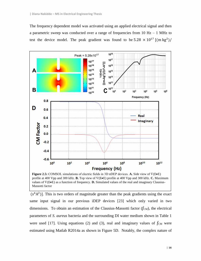
The findings from numerical modelling are shown in Figure 15. ∇(𝐄 • 𝐄) was computed
for an applied signal of 400 Vpp at 300 kHz. The top view and cross-section view of the
slice plot of ∇(𝐄 • 𝐄) are shown in Figure 2.5A and Figure 2.5B, respectively. A PDMS
structure molded the shape of the microfluidic channel. The analysis accounted for the
DI water medium filling the entire channel. A thin glass slide passivation layer separated
the medium from the activation layer of electrodes. Lastly, metal electrodes beneath the
passivation layer were used to activate the device model. The electrical properties of the
layers considered are shown in Table 1.
| Diana Nakidde – MS in Electrical Engineering Thesis
| 16
The frequency dependent model was activated using an applied electrical signal and then
a parametric sweep was conducted over a range of frequencies from 10 Hz – 1 MHz to
test the device model. The peak gradient was found to be 5.28 × 10¹⁷ [(m kg2)/
(s6A2)]. This is two orders of magnitude greater than the peak gradients using the exact
same input signal in our previous iDEP devices [23] which only varied in two
dimensions. To obtain an estimation of the Clausius-Massotti factor (fCM), the electrical
parameters of S. aureus bacteria and the surrounding DI water medium shown in Table 1
were used [17]. Using equations (2) and (3), real and imaginary values of fCM were
estimated using Matlab R2014a as shown in Figure 5D. Notably, the complex nature of
Figure 2.5: COMSOL simulations of electric fields in 3D πDEP devices. A. Side view of (EE)
profile at 400 Vpp and 300 kHz. B. Top view of (EE) profile at 400 Vpp and 300 kHz. C. Maximum
values of (EE) as a function of frequency. D. Simulated values of the real and imaginary Clausius-
Massotti factor
| Diana Nakidde – MS in Electrical Engineering Thesis
| 17
bacteria cells, the unique oval shape, and the single shell model would further influence
fCM. The generated DEP force experienced by a bacteria in the 3D πDEP is a function of
the simulated results of ∇(𝐄 • 𝐄) and fCM.
As shown in equation 2.1, the DEP force acting on a particle is directly proportional to
∇(𝐄•𝐄). Therefore, because of the higher ∇(𝐄•𝐄) component, a much larger DEP force is
generated by 3D πDEP devices for the same applied signal in comparison to 2D iDEP
devices. Additionally, it is vital to note that electric field gradients in 3D πDEP devices
vary in all three dimensions unlike gradients in 2D πDEP devices that only vary in two
dimensions. The higher electric field gradients in 3D πDEP devices further account for
stronger DEP forces experienced by particles.
The frequency response of the 3D πDEP device is shown in Figure 2.5C. Because the
applied signal is capacitively coupled through a thin 100 µm glass slide that seals the
microfluidic cartridge, the frequency response is analogous to a high pass filter with the
attenuation increasing as the frequency is lowered. A dip in ∇(𝐄 • 𝐄) is observed at 2 kHz
and this is attributed to the device operating near the resonant frequency of the circuit.
There are several impedances both in series and in parallel to the active area of the device
for which ∇(𝐄 • 𝐄) is calculated. This phenomenon is especially enhanced in capacitively
coupled systems. Notably, the magnitude of the electric field gradient does not dip below
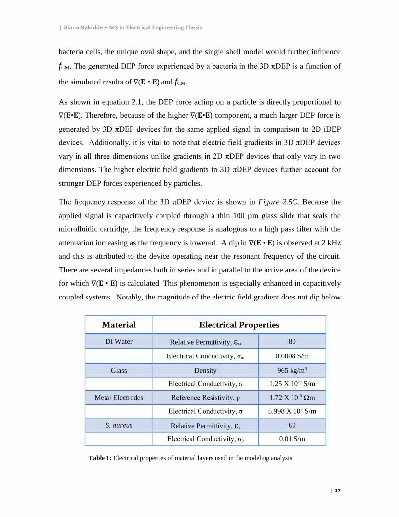
Material Electrical Properties
DI Water Relative Permittivity, εm 80
Electrical Conductivity, σm 0.0008 S/m
Glass Density 965 kg/m3
Electrical Conductivity, σ 1.25 X 10⁻⁹ S/m
Metal Electrodes Reference Resistivity, ρ 1.72 X 10⁻⁸ Ωm
Electrical Conductivity, σ 5.998 X 10⁷ S/m
S. aureus Relative Permittivity, εp 60
Electrical Conductivity, σp 0.01 S/m
Table 1: Electrical properties of material layers used in the modeling analysis
| Diana Nakidde – MS in Electrical Engineering Thesis
| 18
1015 [(m kg2)/ (s6A2)] until the frequency is ~150 Hz. This model therefore predicts the
ability of 3D πDEP devices to operate over a wide frequency range, including very low
frequencies.
B. Frequency Response
DEP trapping experiments with S. aureus were conducted and a signal amplitude of 200
Vpp was maintained at an applied flow rate of 100 μl/hr. The experimental performance
of the 3D πDEP device as a function of the applied frequency is shown in Figure 2.6.
Under these conditions, DEP trapping with 80–100% capture efficiency was observed
over a wide range of frequencies, from 600 Hz to 400 kHz for S. aureus. The reported
results further support predictions from the numerical model. Because the strong DEP
forces generated by the 3D πDEP are greater than 1015[(m kg2)/(s6A2)] over a broad
frequency range, the microfluidic system is highly likely to achieve trapping over a wide
frequency range. However, due to the limited bandwidth of the power amplifier used in
our experiments, a decrease in capture efficiency is observed at higher frequencies.
The results showed that even at the lowest frequency tested (50 Hz), some bacteria were
successfully trapped. At lower frequencies (20-100 kHz), it was observed that trapped
bacteria tended to form extra elongated chains as shown in Figures 2.6 and 2.7. This
behaviour of bioparticles forming pearl chains when trapped in DEP devices has been
previously reported [32]. At high frequencies (<200 kHz), however, trapping of bacteria
was concentrated at the microposts with shorter pearl chains. This is attributed to stronger
pDEP forces at high frequencies than at low frequencies, and these therefore pull the
entire pearl chain to the 3D insulating microposts where the electric field gradient is
greatest. A recorded video showing elongated chains of trapped bacteria at a low applied
frequency of 100 kHz, and the bacteria being pulled in, constricted, and compacted at the
microposts when the applied frequency is increased from 100 kHz to 300 kHz is shown
(See Appendix 1 for the video) [19]. When the applied voltage signal was turned off, all
previously trapped bacteria were released, thus trapping was found to be reversible.
| Diana Nakidde – MS in Electrical Engineering Thesis
| 19
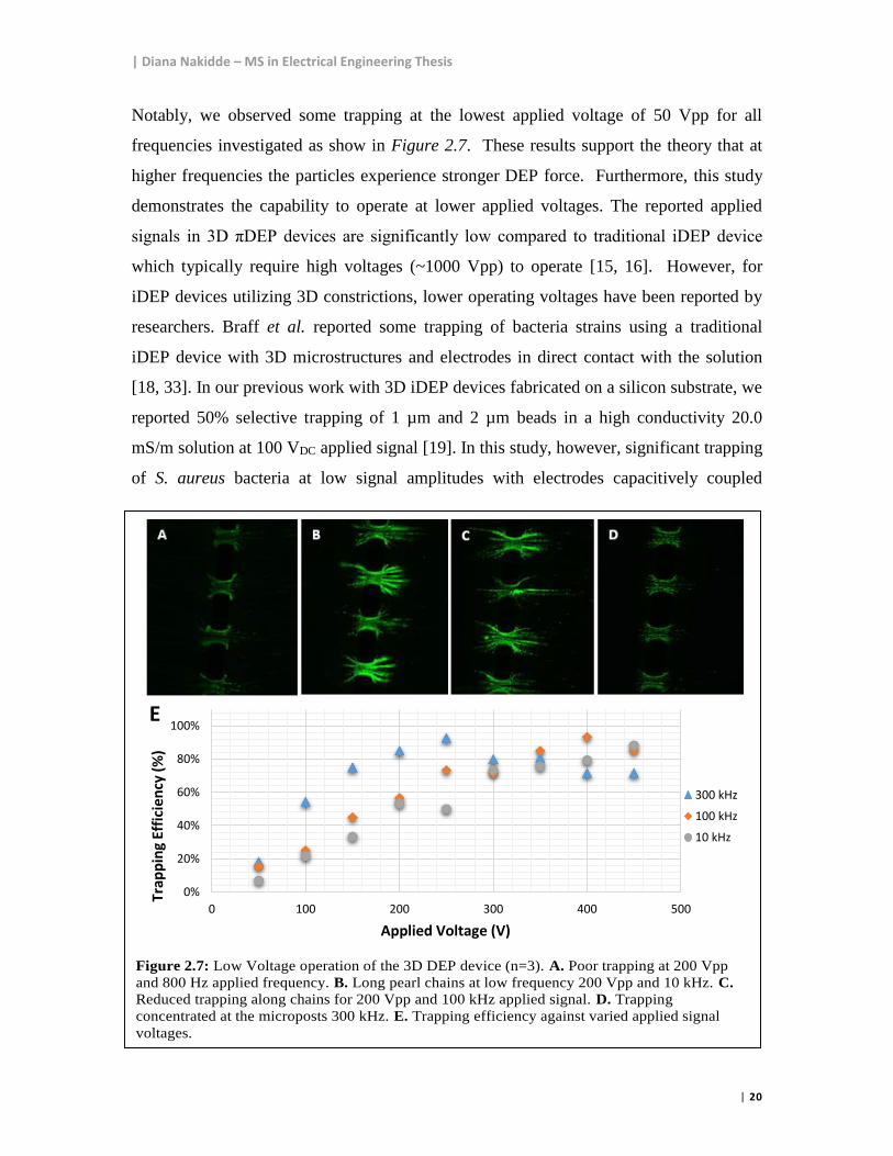
C. Low Voltage Operation
With the frequency held constant, voltage sweeps were conducted over an experimentally
determined device bandwidth. The flow rate was held constant at 100 μl/hr while the
applied signal amplitude was gradually incremented from 0 - 450 Vpp. Variations in
trapping efficiency with changing amplitude were recorded and the results are shown in
Figure 2.7. Results showed that minimum trapping voltage rapidly decreased with
increasing frequency. At 300 kHz, we observed trapping over 80% at voltages as low as
100 Vpp and the trapping gradually increased with increasing applied voltage. At 10
kHz, very low trapping efficiencies were recorded at applied signals below 300 Vpp.
Figure 2.6: Images are of live S. aureus trapping A. 300Hz signal B. 3kHz signal b 30kHz
signal D. 300kHz E. Trapping as a function of frequency (n=3).
0%
20%
40%
60%
80%
100%
50 300 800 50,000 200,000 350,000 500,000 700,000 900,000
Trap
pin
g Ef
fici
ency
(%
)
Frequency (Hz)
E
| Diana Nakidde – MS in Electrical Engineering Thesis
| 20
Notably, we observed some trapping at the lowest applied voltage of 50 Vpp for all
frequencies investigated as show in Figure 2.7. These results support the theory that at
higher frequencies the particles experience stronger DEP force. Furthermore, this study
demonstrates the capability to operate at lower applied voltages. The reported applied
signals in 3D πDEP devices are significantly low compared to traditional iDEP device
which typically require high voltages (~1000 Vpp) to operate [15, 16]. However, for
iDEP devices utilizing 3D constrictions, lower operating voltages have been reported by
researchers. Braff et al. reported some trapping of bacteria strains using a traditional
iDEP device with 3D microstructures and electrodes in direct contact with the solution
[18, 33]. In our previous work with 3D iDEP devices fabricated on a silicon substrate, we
reported 50% selective trapping of 1 µm and 2 µm beads in a high conductivity 20.0
mS/m solution at 100 VDC applied signal [19]. In this study, however, significant trapping
of S. aureus bacteria at low signal amplitudes with electrodes capacitively coupled
Figure 2.7: Low Voltage operation of the 3D DEP device (n=3). A. Poor trapping at 200 Vpp
and 800 Hz applied frequency. B. Long pearl chains at low frequency 200 Vpp and 10 kHz. C.
Reduced trapping along chains for 200 Vpp and 100 kHz applied signal. D. Trapping
concentrated at the microposts 300 kHz. E. Trapping efficiency against varied applied signal
voltages.
0%
20%
40%
60%
80%
100%
0 100 200 300 400 500
Trap
pin
g Ef
fici
ency
(%
)
Applied Voltage (V)
E
300 kHz
100 kHz
10 kHz
| Diana Nakidde – MS in Electrical Engineering Thesis
| 21
through a glass slide has been demonstrated. This 3D πDEP device achieves low voltage
trapping while maintaining high trapping efficiency over a wide range of frequencies.
D. Flow Rate Analysis
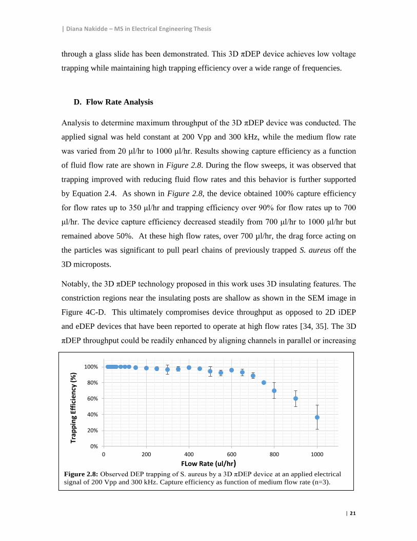
Analysis to determine maximum throughput of the 3D πDEP device was conducted. The
applied signal was held constant at 200 Vpp and 300 kHz, while the medium flow rate
was varied from 20 μl/hr to 1000 μl/hr. Results showing capture efficiency as a function
of fluid flow rate are shown in Figure 2.8. During the flow sweeps, it was observed that
trapping improved with reducing fluid flow rates and this behavior is further supported
by Equation 2.4. As shown in Figure 2.8, the device obtained 100% capture efficiency
for flow rates up to 350 μl/hr and trapping efficiency over 90% for flow rates up to 700
μl/hr. The device capture efficiency decreased steadily from 700 μl/hr to 1000 μl/hr but
remained above 50%. At these high flow rates, over 700 µl/hr, the drag force acting on
the particles was significant to pull pearl chains of previously trapped S. aureus off the
3D microposts.
Notably, the 3D πDEP technology proposed in this work uses 3D insulating features. The
constriction regions near the insulating posts are shallow as shown in the SEM image in
Figure 4C-D. This ultimately compromises device throughput as opposed to 2D iDEP
and eDEP devices that have been reported to operate at high flow rates [34, 35]. The 3D
πDEP throughput could be readily enhanced by aligning channels in parallel or increasing
Figure 2.8: Observed DEP trapping of S. aureus by a 3D πDEP device at an applied electrical
signal of 200 Vpp and 300 kHz. Capture efficiency as function of medium flow rate (n=3).
0%
20%
40%
60%
80%
100%
0 200 400 600 800 1000
Trap
pin
g Ef
fici
ency
(%
)
FLow Rate (ul/hr)
| Diana Nakidde – MS in Electrical Engineering Thesis
| 22
the channel depth and width dimensions. Consequently, the trapping efficiency
deteriorated from here onwards. Therefore, for experiments with an emphasis on high
trapping efficiency, flow rates under 700 μl/hr are preferable whereas in cases where high
throughput is of greater importance, the device can operate above 700 μl/hr.
E. Separation of Particles
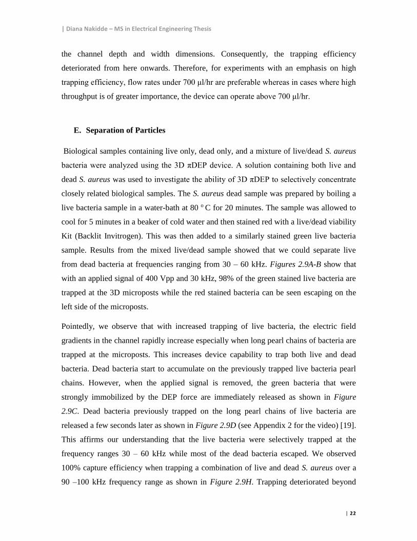
Biological samples containing live only, dead only, and a mixture of live/dead S. aureus
bacteria were analyzed using the 3D πDEP device. A solution containing both live and
dead S. aureus was used to investigate the ability of 3D πDEP to selectively concentrate
closely related biological samples. The S. aureus dead sample was prepared by boiling a
live bacteria sample in a water-bath at 80 o C for 20 minutes. The sample was allowed to
cool for 5 minutes in a beaker of cold water and then stained red with a live/dead viability
Kit (Backlit Invitrogen). This was then added to a similarly stained green live bacteria
sample. Results from the mixed live/dead sample showed that we could separate live
from dead bacteria at frequencies ranging from 30 – 60 kHz. Figures 2.9A-B show that
with an applied signal of 400 Vpp and 30 kHz, 98% of the green stained live bacteria are
trapped at the 3D microposts while the red stained bacteria can be seen escaping on the
left side of the microposts.
Pointedly, we observe that with increased trapping of live bacteria, the electric field
gradients in the channel rapidly increase especially when long pearl chains of bacteria are
trapped at the microposts. This increases device capability to trap both live and dead
bacteria. Dead bacteria start to accumulate on the previously trapped live bacteria pearl
chains. However, when the applied signal is removed, the green bacteria that were
strongly immobilized by the DEP force are immediately released as shown in Figure
2.9C. Dead bacteria previously trapped on the long pearl chains of live bacteria are
released a few seconds later as shown in Figure 2.9D (see Appendix 2 for the video) [19].
This affirms our understanding that the live bacteria were selectively trapped at the
frequency ranges 30 – 60 kHz while most of the dead bacteria escaped. We observed
100% capture efficiency when trapping a combination of live and dead S. aureus over a
90 –100 kHz frequency range as shown in Figure 2.9H. Trapping deteriorated beyond
| Diana Nakidde – MS in Electrical Engineering Thesis
| 23
400 kHz due to bandwidth limitations of the amplifier. It should be noted, however, that
dead bacteria had a tendency to foul the surface and stick to the microposts even after the
applied signal was removed as seen in Figure 2.9D. Fouled bacteria can be removed by
increasing the flow rate prior to the next run.
Figure 2.9: Sample of live and dead bacteria at 400Vpp and 100ul/hr. A, B. Selective trapping of
live bacteria while the dead escape at 30kHz. C. Applied signal is removed and the live bacteria is
immediately released. D. All bacteria is released though some fouls at the posts. E, F. Long pearl
chain formed while trapping a dead bacteria sample at 50kHz and 100kHz. G. Trapping at 300kHz
concentrated at the microposts. H. Superimposed results from purely live, purely dead and mixed
live/dead bacteria frequency runs. (n=3)
A
E
B C D
F G
0%
10%
20%
30%
40%
50%
60%
70%
80%
90%
100%
0.1 1 10 100 1000
Trap
pin
g Ef
fici
en
cy (
%)
Applied Frequency (kHz)
H
Dead Sample
Live Sample
Live/Dead-LiveTrappingLive/Dead-DeadTrapping
| Diana Nakidde – MS in Electrical Engineering Thesis
| 24
As seen previously with live S. aureus samples, Figures 2.9E-G show trapping of dead
bacteria with extra-long pearl chains formed at lower frequencies, 10–100 kHz. At higher
frequencies (<250 kHz), the trapping was concentrated at the microposts due to the
particle experiencing a stronger DEP force. To fine tune selectivity of the device, a
frequency sweep for a purely dead S. aureus sample was obtained and interposed this
with results from a purely live sample as shown in Figure 2.9H. The live sample (Green)
consisted of only live bacteria. Results showed a trapping efficiency over 80% for
frequencies ranging from 600Hz to 400 kHz and maximum trapping efficiency starting at
60 kHz. The more bacteria are trapped in elongated pearls, the more the electrical field
gradient is enhanced within the channel further increasing the trapping efficiency.
Notably beyond 400 kHz, the power amplifier starts to attenuate causing a sudden drop in
the trapping efficiency. The same is true for Dead sample containing dead bacteria.
However, we can easily observe that increase in the trapping efficiency of dead bacteria
happens closer to 100 kHz and there is distinct efficiency between live and dead sample
when it comes to frequencies between 1-70 kHz.
The Live/Dead sample consisted of a mixture of live and dead bacteria. Using ImageJ, we
analyzed the trapping efficiency of live (Blue) and dead (Purple) bacteria in the mixed
sample population. It should be noted that trapping can affect the local electric field
gradient and hence, the trapping efficiency observed for the dead bacteria in the mixed
population can be influenced by the trapping of live bacteria that can happen at lower
frequencies. Nevertheless, we can see a more distinct separation between the live and
dead bacteria at frequencies close to 60 kHz while at frequencies around 100 kHz, the
trapping efficiency of the entire sample is close to 100%. Again, due to limitations in the
power amplifier, we could not conclude if the chip is capable of efficiently separating the
live and dead bacteria at higher frequencies.
2.5 Discussion and Conclusion
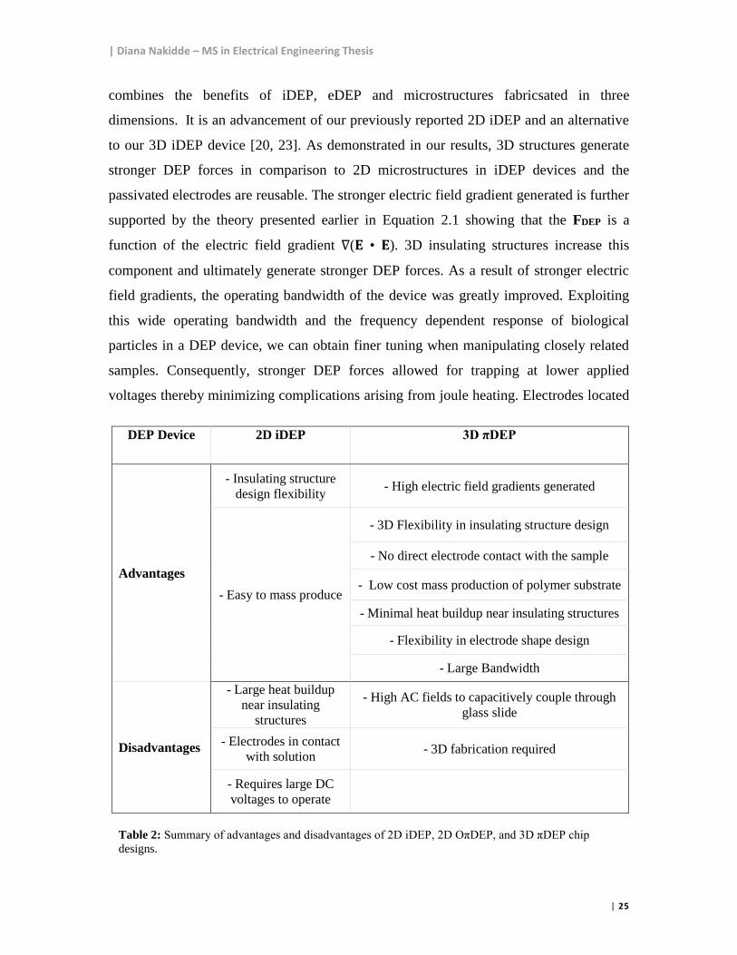
In this paper, we have introduced the first reported 3D πDEP device capable of achieving
high capture efficiencies and separation of biological particles at low voltages and have
showcased its performance through numerical models and experiments. 3D πDEP
| Diana Nakidde – MS in Electrical Engineering Thesis
| 25
DEP Device 2D iDEP 3D πDEP
Advantages
- Insulating structure
design flexibility - High electric field gradients generated
- Easy to mass produce
- 3D Flexibility in insulating structure design
- No direct electrode contact with the sample
- Low cost mass production of polymer substrate
- Minimal heat buildup near insulating structures
- Flexibility in electrode shape design
- Large Bandwidth
Disadvantages
- Large heat buildup
near insulating
structures
- High AC fields to capacitively couple through
glass slide
- Electrodes in contact
with solution - 3D fabrication required
- Requires large DC
voltages to operate
Table 2: Summary of advantages and disadvantages of 2D iDEP, 2D OπDEP, and 3D πDEP chip
designs.
combines the benefits of iDEP, eDEP and microstructures fabricsated in three
dimensions. It is an advancement of our previously reported 2D iDEP and an alternative
to our 3D iDEP device [20, 23]. As demonstrated in our results, 3D structures generate
stronger DEP forces in comparison to 2D microstructures in iDEP devices and the
passivated electrodes are reusable. The stronger electric field gradient generated is further
supported by the theory presented earlier in Equation 2.1 showing that the FDEP is a
function of the electric field gradient ∇(𝐄 • 𝐄). 3D insulating structures increase this
component and ultimately generate stronger DEP forces. As a result of stronger electric
field gradients, the operating bandwidth of the device was greatly improved. Exploiting
this wide operating bandwidth and the frequency dependent response of biological
particles in a DEP device, we can obtain finer tuning when manipulating closely related
samples. Consequently, stronger DEP forces allowed for trapping at lower applied
voltages thereby minimizing complications arising from joule heating. Electrodes located
| Diana Nakidde – MS in Electrical Engineering Thesis
| 26
within the vicinity of the 3D microstructures reduce path travelled by current when the
applied signal is turned and ultimately minimize heat buildup in the entire microfluidic
channel. Heat buildup in the microfluidic channel can result in device failure [27] and
potentially reduce sample viability in biological applications. Therefore 3D πDEP
devices can be operated for longer durations with minimal temperature effects on the
biological sample. Additionally, by capacitively coupling through an insulating layer, the
electrodes are never in direct contact with the solution thus avoiding sample
contamination and gas evolution. These reported advances in performance are obtained
while maintaining a simple, low cost, single etch, single mask, polymer mold fabrication.
The device ability to operate at lower applied voltages minimizes chances of cell death
due to electroporation. To further curb this problem, the applied signal was turned on in
short bursts during trapping and turned off after. The channel design of 3D insulating
microstructures improves the electric field gradients, ultimately increasing the DEP force
acting on bioparticles. Capture efficiency of 100% was achieved for an applied voltage of
200 Vpp over a wide frequency bandwidth ranging from 600 Hz – 400 kHz. Because
trapping of microparticles is concentrated at the microposts, the device throughput can be
improved by widening the microchannel. To characterize different biological samples,
the applied signal amplitude and frequency as well as a combination of AC and DC
signals can be manipulated to selectively trap bioparticles. Moreover, the 3D πDEP
devices can be customized by changing the electrode and 3D insulating structures to
achieve high selectivity of closely related bioparticles. This 3D πDEP device offers the
capability for low cost disposable testing of water samples in the field. Additionally, the
low frequency operation of the device allows for exploitation of a wider frequency range
on the DEP spectrum when investigating different biological samples. A summary of the
advantages and disadvantages of 2D iDEP and 3D πDEP microfluidic designs are shown
in Table 2.
The reported results showcase the promising potential of the 3D πDEP device as a low
cost, high throughput and highly efficient platform for biological sample analysis for
applications ranging from pathogen manipulation to medical and therapeutic diagnostics.
Furthermore, the passivated electrodes offer reusability and flexibility in electrode
design.
| Diana Nakidde – MS in Electrical Engineering Thesis
| 27
3.0 TRAPPING OF SUBMICRON PARTICLES USING 3D
EMBEDDED-ELECTRODE INSULATOR-BASED
DIELECTROPHORESIS
This work was presented in a poster at the Biomedical Engineering Society (BMES)
annual meeting, 2014. BMES serves as a leading society and professional home for
biomedical and bioengineering research.
3.1 Introduction
Submicron bioparticles such as protein, yeast, bacteria and viruses can be detected,
manipulated and characterized using dielectrophoresis [36]. Using positive
dielectrophoresis, researchers have successfully demonstrated nanoparticle manipulation
by precipitating DNA and protein samples [37]. Integration of this DEP technology onto
a lab on a Chip system capable of analyzing virus-sized particles would avail a low cost
diagnostic tool.
In this study, we present for the first time a 3D embedded-electrode insulator-based
dielectrophoresis device (3D iDEP) used to detect and trap submicron particles (0.5µm
beads). The device has 3D insulating features that increase the electric field gradient in
the microchannel and ultimately generate stronger DEP forces [9, 38]. Device
performance is complimented by the embedded electrodes passivated by a thin layer of
polydimethylsiloxane (PDMS) polymer. This allows for device activation within the
vicinity of the microposts without favoring heating effects that arise when the electrodes
are in direct contact with the solution [19]. Submicron particle trapping efficiencies <
90% are reported over a wide frequency range of 2 kHz – 300 kHz at 0.1 µl/hr and
300Vpp.
| Diana Nakidde – MS in Electrical Engineering Thesis
| 28
3.2 Theory
Dielectrophoresis is the motion of neutrally charged polarizable particles due to a non –
uniform electric field. Polarization occurs when the distribution of charge within a
particle is distorted due to an external field. Dielectrophoretic behavior of the particle is
dependent on size and the electrical properties of the particle. It’s on the basis of this
concept that selectivity can be achieved using dielectrophoresis (DEP). The time average
DEP force acting on a particle in an electric field, E is given by:
32 ReDEP CMmF R f E E (3.1)
where R is the particle radius, Re [fCM] is the real part of the Clausius-Massotti factor.
fCM is a measure of the polarizability of a particle and it is given by:
2
CM
p m
p m
f
(3.2)
where εp * and εm * are complex permittivities of the particle and medium respectively.
fCM not only depends on complex permittivities but also on the frequency of the applied
signal. This accounts for the DEP force varying with frequency. The real part of fCM
varies from (1 < Re [fCM] < - 0.5 and will therefore generate a positive or negative DEP
force.
Particles in microfluidic systems will also experience a drag force given by Stokes law:
𝑭𝐷𝑟𝑎𝑔 = −𝑓𝑣 (3.3)
where f is the friction factor of the particle. For low Reynold numbers, the friction factor
of spherical particles is:
𝑓 = 6𝜋𝜂𝑟 (3.4)
Not accounting for Brownian motion and the buoyancy force, the equation of motion for
the particle in a DEP microfluidic system is given by:
| Diana Nakidde – MS in Electrical Engineering Thesis
| 29
𝑚 𝑑𝑣
𝑑𝑡= 𝑭𝐷𝐸𝑃 − 𝑭𝐷𝑟𝑎𝑔 (3.5)
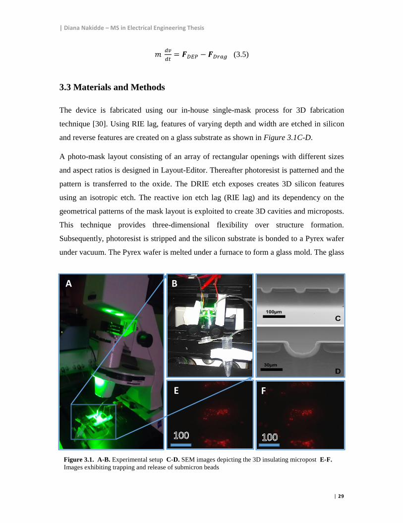
3.3 Materials and Methods
The device is fabricated using our in-house single-mask process for 3D fabrication
technique [30]. Using RIE lag, features of varying depth and width are etched in silicon
and reverse features are created on a glass substrate as shown in Figure 3.1C-D.
A photo-mask layout consisting of an array of rectangular openings with different sizes
and aspect ratios is designed in Layout-Editor. Thereafter photoresist is patterned and the
pattern is transferred to the oxide. The DRIE etch exposes creates 3D silicon features
using an isotropic etch. The reactive ion etch lag (RIE lag) and its dependency on the
geometrical patterns of the mask layout is exploited to create 3D cavities and microposts.
This technique provides three-dimensional flexibility over structure formation.
Subsequently, photoresist is stripped and the silicon substrate is bonded to a Pyrex wafer
under vacuum. The Pyrex wafer is melted under a furnace to form a glass mold. The glass
Figure 3.1. A-B. Experimental setup C-D. SEM images depicting the 3D insulating micropost E-F.
Images exhibiting trapping and release of submicron beads
A B
E F
| Diana Nakidde – MS in Electrical Engineering Thesis
| 30
substrate master mold is left behind after the silicon substrate is etched away using KOH
etch procedure. Low cost PDMS devices are mass produced using the glass master mold.
The multiple device PDMS polymer are carefully peeled off the mold, cut into single
devices, and 2 mm holes are punched into the microfluidic channels for fluidic ports. The
devices are sealed by plasma bonding, using a Plasma Cleaner (Harrick Plasma), to a
glass cover-slide (Electron Microscopy Sciences) forming the microfluidic cartridge.
Sub-micron (0.5 µm) beads were suspended in DI water with a measured conductivity
800 µS/m. The experimental setup is as shown in Figure 3.1A-B. The microfluidic
cartridge is mounted onto the Zeiss inverted microscope (Model - Z100) stage and
secured in place using paper tape. A 1 ml syringe containing suspended sub-micron beads
is then fitted onto the syringe pump and connected to the 3D πDEP device inlet port. As
shown in Figure 3.1B, tubing is connected from the outlet port to waste microtube.
Submicron particles are pressure driven through the device using a Harvard Apparatus
syringe pump at 0.1 µl/hr. 300 Vpp AC voltage signal is applied across the microposts to
activate the device. A frequency sweep ranging from 10 Hz – 450 kHz is conducted and
trapping efficiency is measured. Extracted results of trapping efficiency are shown in
Figure 3.2.
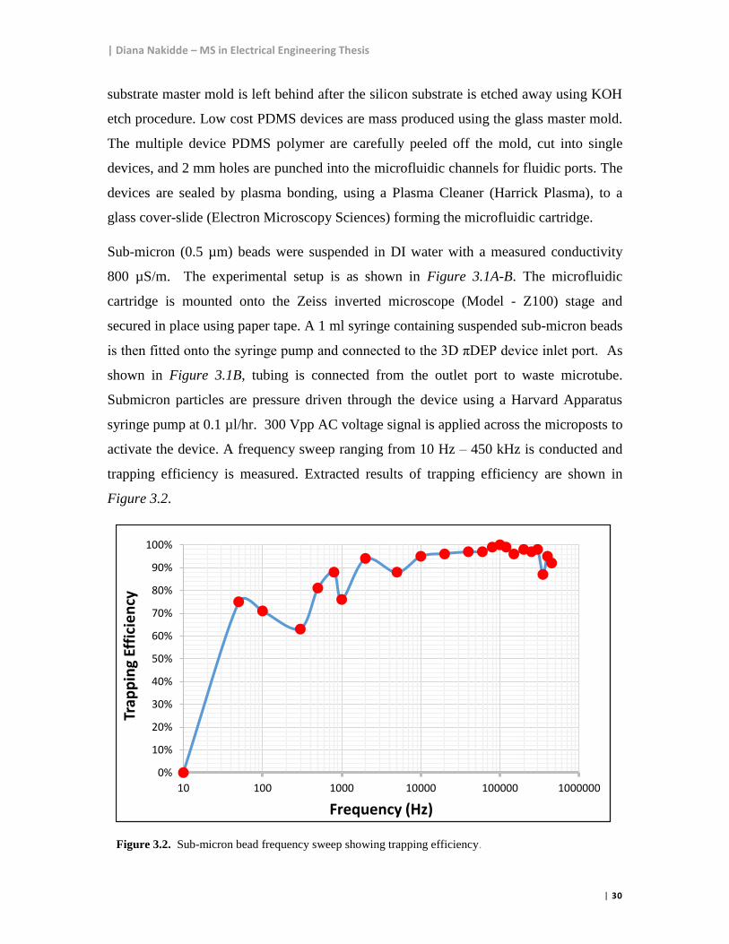
Figure 3.2. Sub-micron bead frequency sweep showing trapping efficiency.
0%
10%
20%
30%
40%
50%
60%
70%
80%
90%
100%
10 100 1000 10000 100000 1000000
Trap
pin
g Ef
fici
en
cy
Frequency (Hz)
| Diana Nakidde – MS in Electrical Engineering Thesis
| 31
3.4 Results and Discussion
In this work, trapping of submicron particles at trapping efficiencies over 90% is
demonstrated over a wide frequency range. With insulator based dielectrophoresis
devices (iDEP), DEP forces are generated due to non-uniform electric field gradients at
the insulating microposts. In this case, the 3D nature of the insulating posts increases the
electric field gradients, and as a result stronger DEP forces are generated. When the
applied signal is turned on, the submicron beads are observed to trap at the 3D insulating
microposts as shown in Figure 3.1E.
In Figure 3.1F the signal is turned off and the beads are released to the left hand side of
the posts. In Figure 3.2, results show the device’s capability to operate with high
trapping efficiency even at low applied frequencies. The frequency sweep shows high
trapping efficiency over 90% for applied signals ranging from 2 kHz – 300 kHz and
greater than 60% trapping efficiency for lower frequencies between 50Hz - 1000Hz. This
is demonstrates the wide frequency range operation of 3D iDEP. Additionally, because
the electrical properties beads do not change significantly as the frequency changes, these
results further support that concept. However, due to slight changes is surfaces properties
of the beads at different frequencies, variations are reported. The particle size and
magnitude of the generated electric field gradient play a bigger role in determining the
DEP force experienced by the sub-micron particles.
This work demonstrated the ability to detect and trap sub-micron particles. Results
presented point to the capability of implementing 3D iDEP devices that can successfully
detect, trap and characterize submicron particles with biological applicability. Real life
submicron sized bioparticles like viruses, DNA, protein, chromosomes, and bacteria
could be analyzed with further advancement in this technology. The unique electrical
properties of the bioparticles would facilitate selective trapping of closely related
samples.
| Diana Nakidde – MS in Electrical Engineering Thesis
| 32
4.0 HIGH THROUGHPUT 3D IDEP
4.1 Introduction
In 3D πDEP systems, microparticles are trapped and isolated using insulating
microstructures. Due to the nature of enhanced graduate profiles of the insulating
structures, the throughput capability of the device is compromised. Considering that
most real life sample populations are in relatively large volumes, it is beneficial to further
enhance 3D iDEP device performance by increasing device throughput.
One of the ways that device throughput can be improved is by designing multiple iDEP
microfluidics channels in parallel. This would ultimately increase throughput by a factor
of the number of channels added. In this case, device throughput is increased without
compromising device trapping efficiency. Alternatively, increasing microchannel width
and height dimensions would also increase device throughput. However this would be at
the expense of device trapping efficiency. Furthermore, increasing the external fluid
pump pressure would also increase device throughput. This case, however, adversely
increases the drag force acting on the bioparticles and stronger DEP force would be
required to achieve the same trapping efficiency.
4.2 Methods and Materials
Configurations of high throughput 3D iDEP devices have been investigated and the
designs are shown in Figure 4.1 below. Devices were fabricated using our in-house
developed 3D micromachining technique discussed in Chapter 2 [31].
Briefly, a silicon wafer is patterned with photoresist and etched using an Alcatel AMS-
100 Deep Reactive Ion Etcher (DRIE) to obtain 3D insulating structures. A Pyrex wafer
is anodically bonded to the etched silicon wafer under vacuum. The glass mold is then
cured in a heated chamber after which the silicon wafer is stripped using a KOH
procedure. Liquid PDMS is poured onto the glass mold and cured. Finally, the PDMS is
plasma bonded to a cover glass to form the microfluidic cartridge. Figure 4.3 shows the
fabricated devices. The operating principle of these devices is to concentrate the bacteria
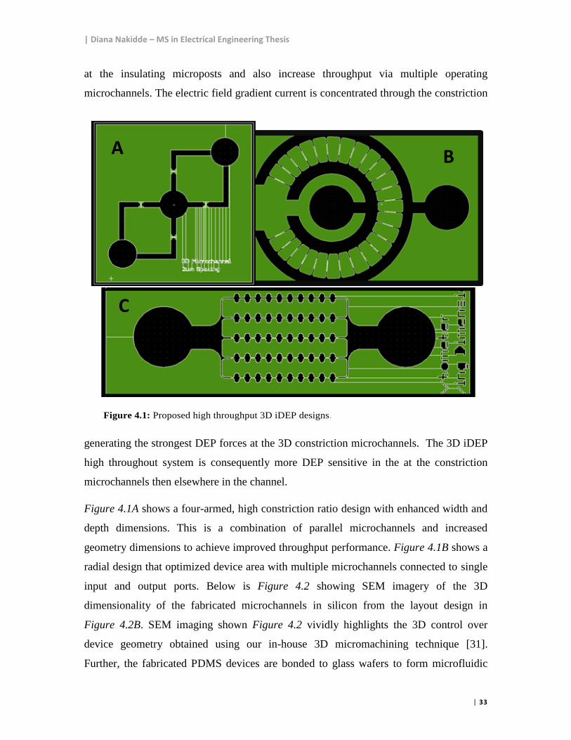
| Diana Nakidde – MS in Electrical Engineering Thesis
| 33
Figure 4.1: Proposed high throughput 3D iDEP designs.
A B
C
at the insulating microposts and also increase throughput via multiple operating
microchannels. The electric field gradient current is concentrated through the constriction
generating the strongest DEP forces at the 3D constriction microchannels. The 3D iDEP
high throughout system is consequently more DEP sensitive in the at the constriction
microchannels then elsewhere in the channel.
Figure 4.1A shows a four-armed, high constriction ratio design with enhanced width and
depth dimensions. This is a combination of parallel microchannels and increased
geometry dimensions to achieve improved throughput performance. Figure 4.1B shows a
radial design that optimized device area with multiple microchannels connected to single
input and output ports. Below is Figure 4.2 showing SEM imagery of the 3D
dimensionality of the fabricated microchannels in silicon from the layout design in
Figure 4.2B. SEM imaging shown Figure 4.2 vividly highlights the 3D control over
device geometry obtained using our in-house 3D micromachining technique [31].
Further, the fabricated PDMS devices are bonded to glass wafers to form microfluidic
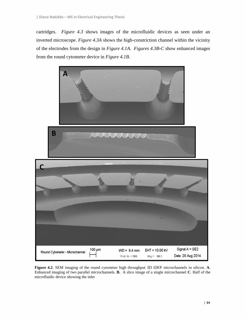
| Diana Nakidde – MS in Electrical Engineering Thesis
| 34
cartridges. Figure 4.3 shows images of the microfluidic devices as seen under an
inverted microscope. Figure 4.3A shows the high-constriction channel within the vicinity
of the electrodes from the design in Figure 4.1A. Figures 4.3B-C show enhanced images
from the round cytometer device in Figure 4.1B.
A
B
C
Figure 4.2. SEM imaging of the round cytometer high throughput 3D iDEP microchannels in silicon. A.
Enhanced imaging of two parallel microchannels. B. A slice image of a single microchannel C. Half of the
microfluidic device showing the inlet
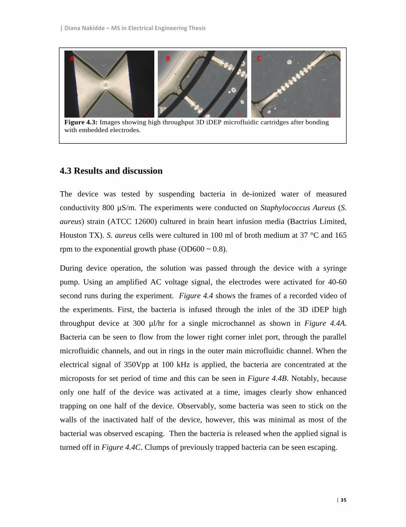
| Diana Nakidde – MS in Electrical Engineering Thesis
| 35
Figure 4.3: Images showing high throughput 3D iDEP microfluidic cartridges after bonding
with embedded electrodes.
A B C
4.3 Results and discussion
The device was tested by suspending bacteria in de-ionized water of measured
conductivity 800 µS/m. The experiments were conducted on Staphylococcus Aureus (S.
aureus) strain (ATCC 12600) cultured in brain heart infusion media (Bactrius Limited,
Houston TX). S. aureus cells were cultured in 100 ml of broth medium at 37 °C and 165
rpm to the exponential growth phase (OD600 ~ 0.8).
During device operation, the solution was passed through the device with a syringe
pump. Using an amplified AC voltage signal, the electrodes were activated for 40-60
second runs during the experiment. Figure 4.4 shows the frames of a recorded video of
the experiments. First, the bacteria is infused through the inlet of the 3D iDEP high
throughput device at 300 µl/hr for a single microchannel as shown in Figure 4.4A.
Bacteria can be seen to flow from the lower right corner inlet port, through the parallel
microfluidic channels, and out in rings in the outer main microfluidic channel. When the
electrical signal of 350Vpp at 100 kHz is applied, the bacteria are concentrated at the
microposts for set period of time and this can be seen in Figure 4.4B. Notably, because
only one half of the device was activated at a time, images clearly show enhanced
trapping on one half of the device. Observably, some bacteria was seen to stick on the
walls of the inactivated half of the device, however, this was minimal as most of the
bacterial was observed escaping. Then the bacteria is released when the applied signal is
turned off in Figure 4.4C. Clumps of previously trapped bacteria can be seen escaping.
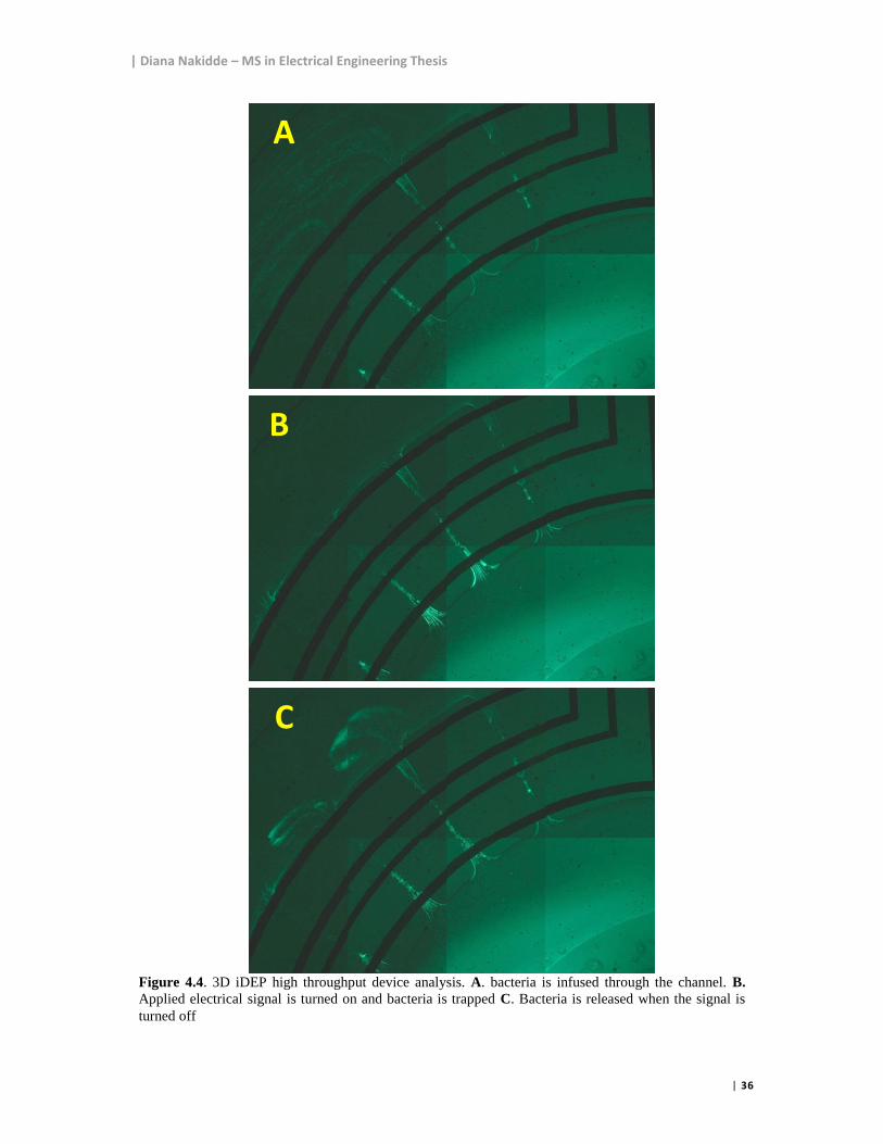
| Diana Nakidde – MS in Electrical Engineering Thesis
| 36
A
B
C
Figure 4.4. 3D iDEP high throughput device analysis. A. bacteria is infused through the channel. B.
Applied electrical signal is turned on and bacteria is trapped C. Bacteria is released when the signal is
turned off
| Diana Nakidde – MS in Electrical Engineering Thesis
| 37
4.4 Outlook and Conclusion
These results demonstrate that it is possible to improve iDEP device throughput
performance without compromising DEP trapping efficiency. These reported results were
conducted at 300 µl/hr, which is three times the flow rate reported in our previous
experiments [39]. This is without accounting for the 28 parallel microchannels that
increase the volume of the constriction insulating microstructures. These parallel
microchannels ultimately increase the overall device throughput per run. Notably, the
device geometry also maximizes device area with a single inlet in the middle of the
device and a single outlet for all parallel microchannels.
It may be possible to improve the DEP performance of this system by incorporating 3D
insulating posts. The current device design exploits sinuated 3D microchannel walls to
generate non- uniform electric field gradients. 3D insulating posts would further increase
the electric field gradient generated and therefore increase the DEP force generated.
Additionally, the device could be made more robust by eliminating the reference
electrode pairs that were added for multi-frequency or zone analysis. Results showed that
these interfered with the electric field gradient when inactivated by acting as an insulating
structure in the channel. Different zones could be investigated by designing different
electrode designs and then investigated these individually. Alternatively, passivated
electrodes with multiple electrode combination were less susceptible to interfering with
the system when inactivated.
| Diana Nakidde – MS in Electrical Engineering Thesis
| 38
5. CONCLUSIONS AND FUTURE WORK
5.0 Summary of Results
In this work, an in-house developed technique is used to fabricate microfluidic devices that
exploit the physics of three-dimensional insulator based dielectrophoresis (3D iDEP) to
characterize, analyze and isolate bioparticles. These discussed systems employ large
constriction ratios of 3D fabricated channels to generate high electric field gradients and
ultimately stronger DEP forces in comparison to traditional two dimensional (2D) systems.
Consequently, the trapping and characterization capability of small, closely related
microparticles is made feasible. In Chapter 2, it has been demonstrated that device
performance is significantly improved by 3D insulator based devices in comparison to 2D
iDEP devices.
Despite tremendous progress in the field of iDEP over the recent years, commercialization
still poses a daunting task due to the high costs associated with these systems. Most of this
has been attributed to costly fabrication procedures accompanied by expensive supporting
equipment used. The fabrication techniques presented in this work are yet another step in
the right direction. A single DRIE etch step is used to create 3D features with a single
mask. Furthermore, microfluidic devices are batch fabricated in low-cost PDMS polymer.
Even more importantly, millions of lives are affected every year as a result of waterborne
pathogens and microbial diseases. While solutions to this problem may exist today, many
of the current technologies are expensive and inapplicable to all regions of the world. In
this work, MEMS technology is employed to advance existing systems or offer alternative
accessible solutions through highly efficient, low-cost pathogen detection MEMS systems.
5.1 Pulsed iDEP trapping
5.2.1 Introduction
Controlled trapping and separation of microparticles in microfluidic devices is very
important especially because of its potential application in the analysis of bioparticles.
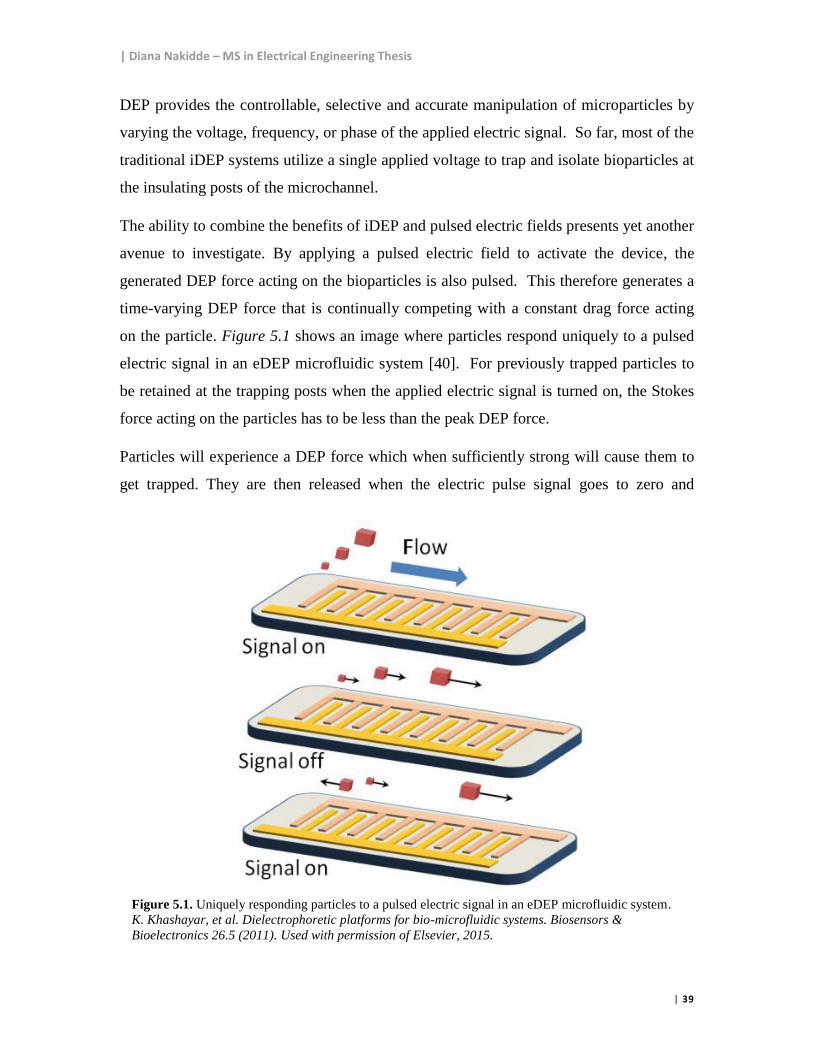
| Diana Nakidde – MS in Electrical Engineering Thesis
| 39
DEP provides the controllable, selective and accurate manipulation of microparticles by
varying the voltage, frequency, or phase of the applied electric signal. So far, most of the
traditional iDEP systems utilize a single applied voltage to trap and isolate bioparticles at
the insulating posts of the microchannel.
The ability to combine the benefits of iDEP and pulsed electric fields presents yet another
avenue to investigate. By applying a pulsed electric field to activate the device, the
generated DEP force acting on the bioparticles is also pulsed. This therefore generates a
time-varying DEP force that is continually competing with a constant drag force acting
on the particle. Figure 5.1 shows an image where particles respond uniquely to a pulsed
electric signal in an eDEP microfluidic system [40]. For previously trapped particles to
be retained at the trapping posts when the applied electric signal is turned on, the Stokes
force acting on the particles has to be less than the peak DEP force.
Particles will experience a DEP force which when sufficiently strong will cause them to
get trapped. They are then released when the electric pulse signal goes to zero and
Figure 5.1. Uniquely responding particles to a pulsed electric signal in an eDEP microfluidic system.
K. Khashayar, et al. Dielectrophoretic platforms for bio-microfluidic systems. Biosensors &
Bioelectronics 26.5 (2011). Used with permission of Elsevier, 2015.
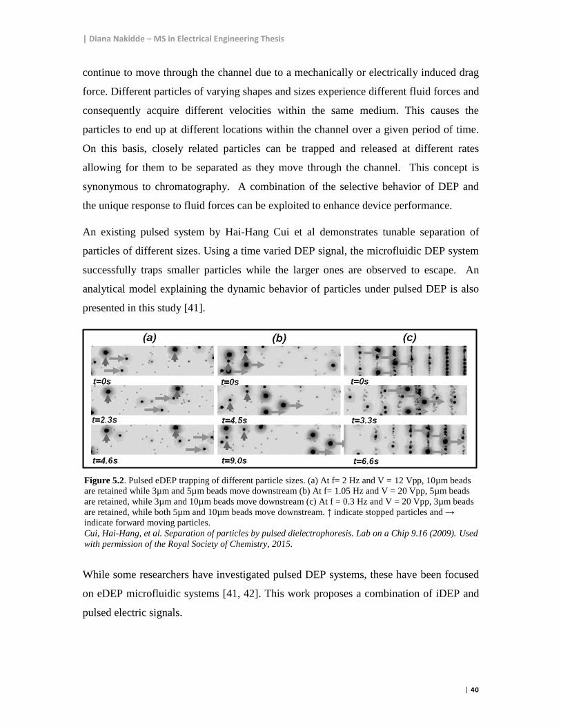
| Diana Nakidde – MS in Electrical Engineering Thesis
| 40
continue to move through the channel due to a mechanically or electrically induced drag
force. Different particles of varying shapes and sizes experience different fluid forces and
consequently acquire different velocities within the same medium. This causes the
particles to end up at different locations within the channel over a given period of time.
On this basis, closely related particles can be trapped and released at different rates
allowing for them to be separated as they move through the channel. This concept is
synonymous to chromatography. A combination of the selective behavior of DEP and
the unique response to fluid forces can be exploited to enhance device performance.
An existing pulsed system by Hai-Hang Cui et al demonstrates tunable separation of
particles of different sizes. Using a time varied DEP signal, the microfluidic DEP system
successfully traps smaller particles while the larger ones are observed to escape. An
analytical model explaining the dynamic behavior of particles under pulsed DEP is also
presented in this study [41].
While some researchers have investigated pulsed DEP systems, these have been focused
on eDEP microfluidic systems [41, 42]. This work proposes a combination of iDEP and
pulsed electric signals.
Figure 5.2. Pulsed eDEP trapping of different particle sizes. (a) At f= 2 Hz and V = 12 Vpp, 10µm beads
are retained while 3µm and 5µm beads move downstream (b) At f= 1.05 Hz and V = 20 Vpp, 5µm beads
are retained, while 3µm and 10µm beads move downstream (c) At f = 0.3 Hz and V = 20 Vpp, 3µm beads
are retained, while both 5µm and 10µm beads move downstream. ↑ indicate stopped particles and →
indicate forward moving particles.
Cui, Hai-Hang, et al. Separation of particles by pulsed dielectrophoresis. Lab on a Chip 9.16 (2009). Used
with permission of the Royal Society of Chemistry, 2015.
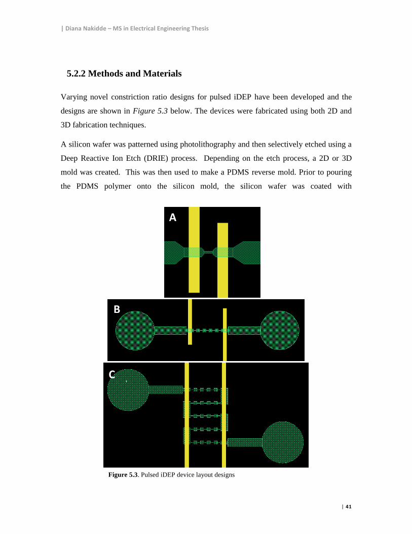
| Diana Nakidde – MS in Electrical Engineering Thesis
| 41
5.2.2 Methods and Materials
Varying novel constriction ratio designs for pulsed iDEP have been developed and the
designs are shown in Figure 5.3 below. The devices were fabricated using both 2D and
3D fabrication techniques.
A silicon wafer was patterned using photolithography and then selectively etched using a
Deep Reactive Ion Etch (DRIE) process. Depending on the etch process, a 2D or 3D
mold was created. This was then used to make a PDMS reverse mold. Prior to pouring
the PDMS polymer onto the silicon mold, the silicon wafer was coated with
B
C
A
Figure 5.3. Pulsed iDEP device layout designs
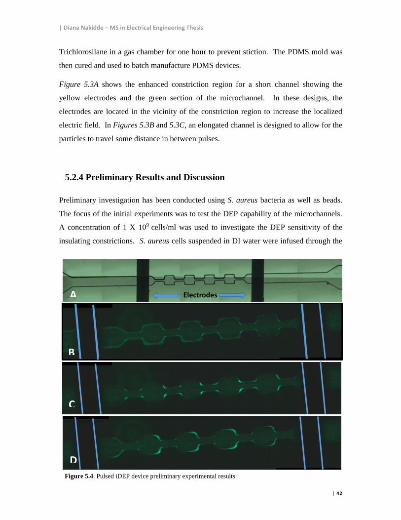
| Diana Nakidde – MS in Electrical Engineering Thesis
| 42
Trichlorosilane in a gas chamber for one hour to prevent stiction. The PDMS mold was
then cured and used to batch manufacture PDMS devices.
Figure 5.3A shows the enhanced constriction region for a short channel showing the
yellow electrodes and the green section of the microchannel. In these designs, the
electrodes are located in the vicinity of the constriction region to increase the localized
electric field. In Figures 5.3B and 5.3C, an elongated channel is designed to allow for the
particles to travel some distance in between pulses.
5.2.4 Preliminary Results and Discussion
Preliminary investigation has been conducted using S. aureus bacteria as well as beads.
The focus of the initial experiments was to test the DEP capability of the microchannels.
A concentration of 1 X 10⁹ cells/ml was used to investigate the DEP sensitivity of the
insulating constrictions. S. aureus cells suspended in DI water were infused through the
Electrodes A
B
C
D
Figure 5.4. Pulsed iDEP device preliminary experimental results
| Diana Nakidde – MS in Electrical Engineering Thesis
| 43
2D microchannel at a flow rate of 20 µl/hr using a Harvard-Apparatus syringe pump.
The device shown in Figure 5.4 was designed with 25µm constrictions and 100 µm wide
regional zones along the microfluidic channel. During the DRIE etch process, these
constriction channels are widened as seen in Figure 5.4B. Nonetheless, even with the
diminished constriction ratio, results showed significant DEP device sensitivity.
Results showed that when the electric signal of 350Vpp and 100 kHz was turned on, the
bacteria is trapped in the constriction areas as depicted in Figure 5.4B. Upon turning off
the electric signal, the bacteria is released and can be seen transiting through the
microchannel in Figure 5.4D.
5.2.5 Outlook and Conclusion
Observably, in an attempt to initiate pulsed-DEP trapping, the drag force acting on the
bacteria was too strong that most of the previously trapped bacteria had already left the
insulating microposts. During this study, results showed that pulsed DEP experiments
would be better suited for low concentration samples. This way, the specific particle
samples being investigated are better tracked as they move throughout the channel.
Going forward, beads samples were investigated at a much slower flow rate (< 20 µl/hr)
to allow for sufficient time to apply multiple pulses to the same particle sample.
The observation of trapping at the insulated constrictions is an encouraging step. In
addition, low concentration samples would potentially make particle tracking in a pulsed
DEP system easier. A proposed use of larger samples like beads and mammalian cells in
low concentrations will further aid in this analysis. Additional testing of these proposed
samples is needed before any conclusions can be drawn.
| Diana Nakidde – MS in Electrical Engineering Thesis
| 44
REFERENCES
1. World Health Organization, U.-W., UN-water global analysis and assessment of
sanitation and drinking-water (GLAAS) 2014 - report. 2014.
2. Grabow, W., Waterborne diseases: Update on water quality assessment and
control. Water S. A., 1996. 22(2): p. 193-202.
3. Medema GJ, P. P., Dufour A, Robertson W, Waite M, Hunter P, Kirby R,
Anderson Y, Assessing Microbial Safety of Drinking Water Improving
Approaches and Methods: Improving Approaches and Methods. 2003: OECD
Publishing, World Health Organization.
4. Cabral, J. P., Water microbiology. Bacterial pathogens and water. International
Journal of Environmental Research and Public Health, 2010. 7(10): p. 3657-
3703.
5. Maluf, N. and K. Williams, Introduction to microelectromechanical systems
engineering. 2004: Artech House.
6. Bryzek, J., Impact of MEMS technology on society. Sensors and Actuators A:
Physical, 1996. 56(1): p. 1-9.
7. Whitesides, G. M., The origins and the future of microfluidics. Nature, 2006.
442(7101): p. 368-373.
8. Pohl, H., Appl. Phys., 1951. 22: p. 869-871.
9. Nakidde, D., et al., Three dimensional passivated-electrode insulator-based
dielectrophoresis. Biomicrofluidics, 2015. 9(1): p. 014125.
10. Pohl, H. A., Dielectrophoresis -The Behavior of Neutral Matter in Nonuniform
Electric Fields. Cambridge University Press, Cambridge, UK, 1978(Cambridge
University Press, Cambridge, UK,).
11. Huang, Y., et al., Differences in the AC electrodynamics of viable and non-viable
yeast cells determined through combined dielectrophoresis and electrorotation
studies. Physics in Medicine and Biology, 1992. 37(7): p. 1499.
12. Zhou, R., P. Wang, and H.-C. Chang, Bacteria capture, concentration and
detection by alternating current dielectrophoresis and self-assembly of dispersed
single-wall carbon nanotubes. ELECTROPHORESIS, 2006. 27(7): p. 1376-1385.
13. Hunt, T. P. and R. M. Westervelt, Dielectrophoresis tweezers for single cell
manipulation. Biomedical Microdevices, 2006. 8(3): p. 227-230.
14. Shake, T., et al., Embedded passivated-electrode insulator-based dielectrophoresis
(EπDEP). Analytical and Bioanalytical Chemistry, 2013. 405(30): p. 9825-9833.
15. Davalos, R., et al., Performance impact of dynamic surface coatings on polymeric
insulator-based dielectrophoretic particle separators. Analytical and Bioanalytical
Chemistry, 2008. 390(3): p. 847-855.
16. Martínez-López, J., et al., Characterization of electrokinetic mobility of
microparticles in order to improve dielectrophoretic concentration. Analytical and
Bioanalytical Chemistry, 2009. 394(1): p. 293-302.
17. Sanchis, A., et al., Dielectric characterization of bacterial cells using
dielectrophoresis. Bioelectromagnetics, 2007. 28(5): p. 393-401.
18. Braff, W. A., et al., Dielectrophoresis-Based Discrimination of Bacteria at the
Strain Level Based on Their Surface Properties. PLoS ONE, 2013. 8(10): p.
e76751.
| Diana Nakidde – MS in Electrical Engineering Thesis
| 45
19. Zellner, P. and M. Agah, Silicon insulator-based dielectrophoresis devices for
minimized heating effects. ELECTROPHORESIS, 2012. 33(16): p. 2498-2507.
20. Zellner, P., et al., 3D Insulator-based dielectrophoresis using DC-biased, AC
electric fields for selective bacterial trapping. ELECTROPHORESIS, 2014: p. n/a-
n/a.
21. Kale, A., et al., Numerical modeling of Joule heating effects in insulator-based
dielectrophoresis microdevices. ELECTROPHORESIS, 2013. 34(5): p. 674-683.
22. Sridharan, S., et al., Joule heating effects on electroosmotic flow in insulator-
based dielectrophoresis. Electrophoresis, 2011. 32(17): p. 2274-2281.
23. Zellner, P., et al., Off-chip passivated-electrode, insulator-based dielectrophoresis
(OπDEP). Analytical and Bioanalytical Chemistry, 2013. 405(21): p. 6657-6666.
24. Pohl, H. A. and J. P. Schwar, Factors Affecting Separations of Suspensions in
Nonuniform Electric Fields. Journal of Applied Physics, 1959. 30(1): p. 69-73.
25. Pethig, R., Review article—dielectrophoresis: status of the theory, technology,
and applications. Biomicrofluidics, 2010. 4(2): p. 022811.
26. Castellarnau, M., et al., Dielectrophoresis as a Tool to Characterize and
Differentiate Isogenic Mutants of Escherichia coli. Biophysical journal, 2006.
91(10): p. 3937-3945.
27. P. Sabounchi, D. E. H., M. P. Kanouff, A. E. Harris, and B. A. Simmons, Joule
Heating Effects on Insulator-Based Dielectrophoresis. presented at the Twelfth
International Conferences on Miniaturized Systems for Chemistry and Life
Sciences, San Diego, CA, USA, , 2008.
28. Sabounchi, P., et al., Sample concentration and impedance detection on a
microfluidic polymer chip. Biomedical Microdevices, 2008. 10(5): p. 661-670.
29. Gantz, K., L. Renaghan, and M. Agah, Development of a comprehensive model
for RIE-lag-based three-dimensional microchannel fabrication. Journal of
Micromechanics and Microengineering, 2008. 18(2): p. 025003.
30. Hosseini, Y., P. Zellner, and M. Agah, A Single-Mask Process for 3-D
Microstructure Fabrication in PDMS. Microelectromechanical Systems, Journal
of, 2013. 22(2): p. 356-362.
31. Zellner, P., et al., A fabrication technology for three-dimensional micro total
analysis systems. Journal of Micromechanics and Microengineering, 2010. 20(4).
32. Shafiee, H., et al., Selective isolation of live/dead cells using contactless
dielectrophoresis (cDEP). Lab on a Chip, 2010. 10(4): p. 438-445.
33. Braff, W. A., A. Pignier, and C. R. Buie, High sensitivity three-dimensional
insulator-based dielectrophoresis. Lab on a Chip, 2012. 12(7): p. 1327-1331.
34. Markx, G. H., P. A. Dyda, and R. Pethig, Dielectrophoretic separation of bacteria
using a conductivity gradient. Journal of biotechnology, 1996. 51(2): p. 175-180.
35. Huang, Y., et al., Introducing dielectrophoresis as a new force field for field-flow
fractionation. Biophysical Journal, 1997. 73(2): p. 1118-1129.
36. Morgan, H., M. P. Hughes, and N. G. Green, Separation of Submicron
Bioparticles by Dielectrophoresis. Biophysical Journal, 1999. 77(1): p. 516-525.
37. Washizu, M., et al., Molecular dielectrophoresis of biopolymers. Industry
Applications, IEEE Transactions on, 1994. 30(4): p. 835-843.
| Diana Nakidde – MS in Electrical Engineering Thesis
| 46
38. Zellner, P., et al., 3D Insulator-based dielectrophoresis using DC-biased, AC
electric fields for selective bacterial trapping. ELECTROPHORESIS, 2015. 36(2):
p. 277-283.
39. Zellner, P., et al., Off-chip passivated-electrode, insulator-based dielectrophoresis
(OπDEP). Analytical and bioanalytical chemistry, 2013: p. 1-10.
40. Khoshmanesh, K., et al., Dielectrophoretic platforms for bio-microfluidic
systems. Biosensors and Bioelectronics, 2011. 26(5): p. 1800-1814.
41. Cui, H.-H., et al., Separation of particles by pulsed dielectrophoresis. Lab on a
Chip, 2009. 9(16): p. 2306-2312.
42. Kumemura, M., et al., Single-DNA-molecule trapping with silicon nanotweezers
using pulsed dielectrophoresis. Journal of Micromechanics and
Microengineering, 2011. 21(5): p. 054020.
| Diana Nakidde – MS in Electrical Engineering Thesis
| 47
APPENDIX A: LIST OF PUBLICATIONS
1. Nakidde, Diana, Phillip Zellner, Mohammad Mehdi Alemi, Tyler Shake, Yahya
Hosseini, Maria V. Riquelme, Amy Pruden, and Masoud Agah. "Three dimensional
passivated-electrode insulator-based dielectrophoresis." Biomicrofluidics vol. 9,
no. 1 (2015): 014125.
2. Phillip Zellner, Tyler Shake, Yahya Hosseini, Diana Nakidde, Maria V. Riquelme,
Ali Sahari, Amy Pruden, Bahareh Behkam, and Masoud Agah, "3D insulator-based
dielectrophoresis using DC-biased, AC electric fields for selective bacterial
trapping," Electrophoresis, vol. 36, no. 2, January 2015, pp. 277-283.
3. V. Srinivasaraghavan, D. Aggarwal, H. Babahosseini, D. Nakidde, J. Strobl and M.
Agah, "Analyses of single-cell mechanoelectrical properties via microfluidics,"
IEEE Sensors 2014, November 2014, Valencia, Spain.
4. Diana Nakidde, Phillip Zellner, Mohammad Mehdi Alemi and Masoud Agah,
"Three Dimensional Passivated-Electrode Insulator-Based Dielectrophoresis(3D
πDEP)," 18th International Conference on Miniaturized Systems for Chemistry and
Life Sciences (MicroTAS 2014), October 2014, San Antonio, TX.
5. Diana Nakidde and Masoud Agah, "Trapping of Submicron Beads using 3D
Embedded-electrode Insulator-based Dielectrophoresis (3D-EπDEP)," Biomedical
Engineering Society (BMES) Annual Meeting 2014, October 2014, San Antonio,
TX.
6. Kevin Crowley, Diana Nakidde, Jeff Travis, and Masoud Agah, "Paper-based
MEMS Hair Cell Array," IEEE Sensors 2013, November 2013, Baltimore, MD, pp.
4.