Embed Size (px)
Citation preview
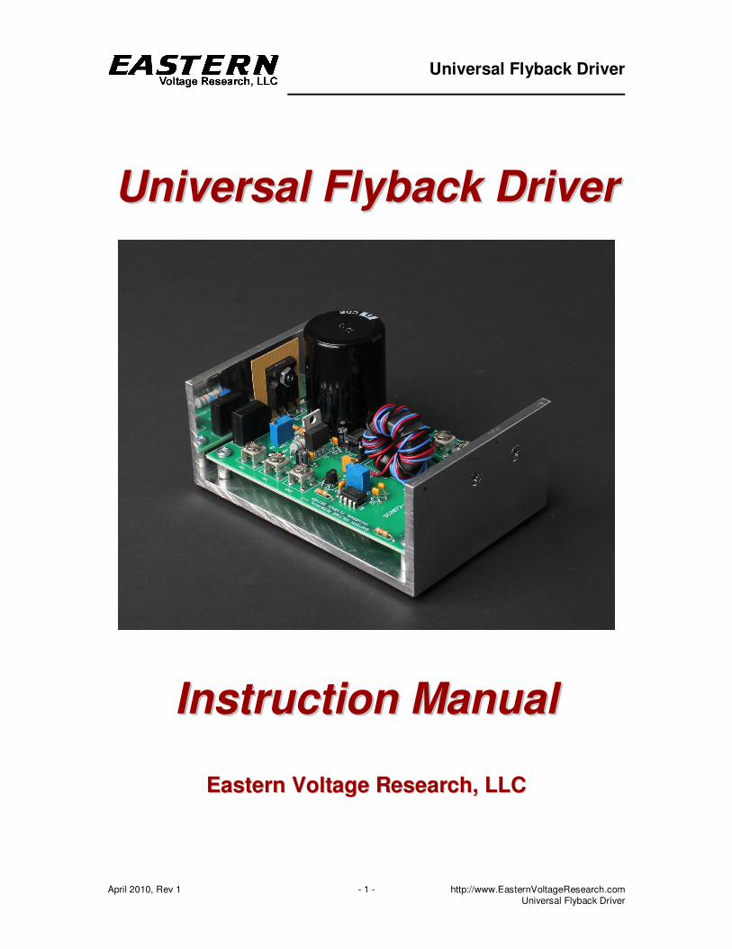
Universal Flyback Driver
April 2010, Rev 1 − 1 − http://www.EasternVoltageResearch.com Universal Flyback Driver
UUnniivveerrssaall FFllyybbaacckk DDrriivveerr
IInnssttrruuccttiioonn MMaannuuaall
EEaasstteerrnn VVoollttaaggee RReesseeaarrcchh,, LLLLCC
Universal Flyback Driver
April 2010, Rev 1 − 2 − http://www.EasternVoltageResearch.com Universal Flyback Driver
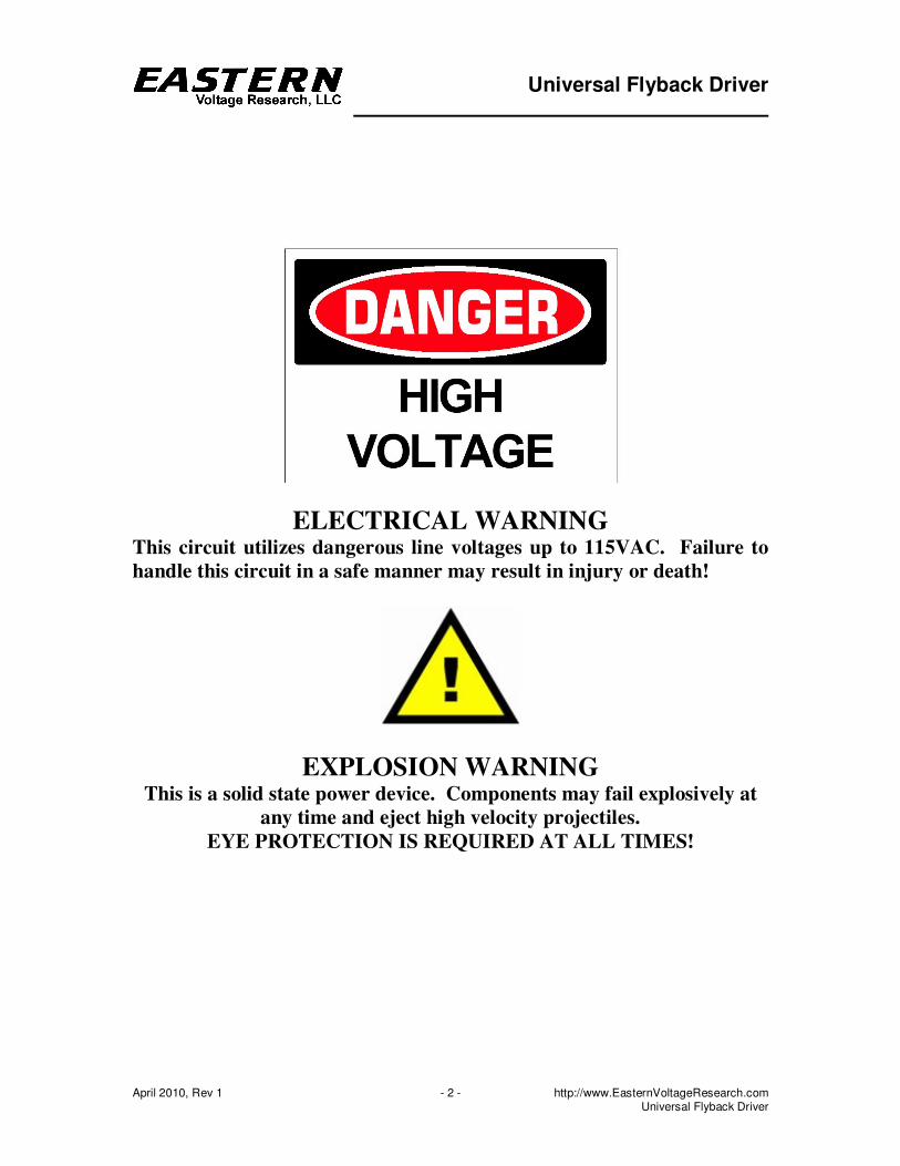
ELECTRICAL WARNING This circuit utilizes dangerous line voltages up to 115VAC. Failure to
handle this circuit in a safe manner may result in injury or death!
EXPLOSION WARNING This is a solid state power device. Components may fail explosively at
any time and eject high velocity projectiles.
EYE PROTECTION IS REQUIRED AT ALL TIMES!
Universal Flyback Driver
April 2010, Rev 1 − 3 − http://www.EasternVoltageResearch.com Universal Flyback Driver
Introduction to the Universal Flyback Driver Thank you for purchasing the Universal Flyback Driver. The Universal Flyback Driver is a high power drive circuit which can be used with virtually all open-core type flyback transformers to generate high voltage arcs. With onboard controls to vary both output frequency and voltage, it’s an extremely flexible design which can be used to drive almost any open-core flyback transformer. Notice to Beginners: If you are a first time kit builder, you may find this instruction manual easier to understand than expected. Each component in this kit has an individual check box, while a detailed description of each component is provided as well. If you follow each step in the instruction manual in order, and practice good soldering and kit building skills, the kit is next to fail-safe.
Please read this manual in its entirety before building, testing, or operating your kit!
Circuit Description The Universal Flyback Driver is an open-loop half-bridge switching power supply. It is called “open loop” as the output voltage is not regulated. Both control and half-bridge power are first rectified and filtered through BR1 and C3 respectively to produce approximately 25-35VDC. Linear regulator, U1 (LM7812) provides the +12VDC control voltage. Transistor, Q1 (N-Channel MOSFET) is utilized as the voltage control device, and with potentiometer R4, the user can vary the output voltage of the flyback driver. The oscillator of the flyback driver utilizes a 555 Timer IC running in astable mode (continuous operation) and has a variable frequency between approximately 5kHz and 120kHz which is controlled via potentiometer, R7. The unique configuration of this 555 Timer circuit provides a nearly 50% duty cycle regardless of the frequency setting. Finally, the 555 Timer output is fed into a high current gate driver, U3, which drives the half-bridge switching transistors (200V N-Channel MOSFETs), Q2 and Q3, whose output is connected directly to the flyback transformer’s primary winding. Gate transformer, T2, provided electrical isolation between the control circuit and the half-bridge switching circuit. This circuit can also be used to drive a solid state Tesla Coil (SSTC) resonator in open-loop mode. Open loop means that the user sets the output frequency, so it wouldn’t be a self-tuning SSTC – it would have to be manually tuned via R7 so that the 555 Timer output frequency matches the resonant frequency of the resonator.
Universal Flyback Driver
April 2010, Rev 1 − 4 − http://www.EasternVoltageResearch.com Universal Flyback Driver
Kit Building Tips
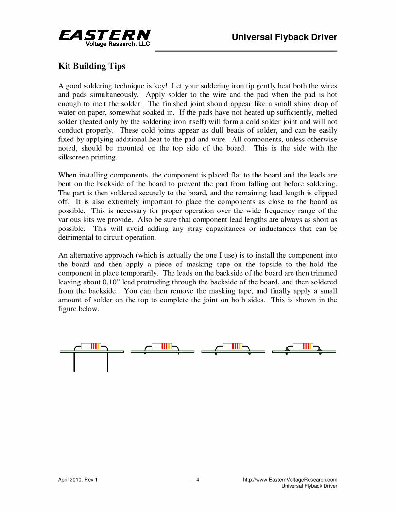
A good soldering technique is key! Let your soldering iron tip gently heat both the wires and pads simultaneously. Apply solder to the wire and the pad when the pad is hot enough to melt the solder. The finished joint should appear like a small shiny drop of water on paper, somewhat soaked in. If the pads have not heated up sufficiently, melted solder (heated only by the soldering iron itself) will form a cold solder joint and will not conduct properly. These cold joints appear as dull beads of solder, and can be easily fixed by applying additional heat to the pad and wire. All components, unless otherwise noted, should be mounted on the top side of the board. This is the side with the silkscreen printing. When installing components, the component is placed flat to the board and the leads are bent on the backside of the board to prevent the part from falling out before soldering. The part is then soldered securely to the board, and the remaining lead length is clipped off. It is also extremely important to place the components as close to the board as possible. This is necessary for proper operation over the wide frequency range of the various kits we provide. Also be sure that component lead lengths are always as short as possible. This will avoid adding any stray capacitances or inductances that can be detrimental to circuit operation. An alternative approach (which is actually the one I use) is to install the component into the board and then apply a piece of masking tape on the topside to the hold the component in place temporarily. The leads on the backside of the board are then trimmed leaving about 0.10” lead protruding through the backside of the board, and then soldered from the backside. You can then remove the masking tape, and finally apply a small amount of solder on the top to complete the joint on both sides. This is shown in the figure below.
Universal Flyback Driver
April 2010, Rev 1 − 5 − http://www.EasternVoltageResearch.com Universal Flyback Driver
Universal Flyback Driver Parts List
RESISTORS
� 2 62 ohm Resistor, 2W (blue-red-black), R1,R10 � 1 3.3k Resistor, 1/2W (orange-orange-red), R2 � 1 10 ohm Resistor (brown-black-black), R5
� 2 5.1 ohm Resistor, 2W (green-brown-gold),R8,R9 � 1 1k ohm Resistor (brown-black-red), R3 � 1 2.2k Resistor (red-red-red), R6 � 2 100k Potentiometer, R4,R7
CAPACITORS
� 4 0.1uF Ceramic Capacitor, C2,C5,C6,C10 � 2 10uF Electrolytic Capacitor, C1,C4 � 1 10uF Tantalum Capacitor, C9 � 1 15000uF 50V Electrolytic Capacitor, C3 � 1 2200pF Ceramic Capacitor, C7 � 1 0.01uF Ceramic Capacitor (marked M39014/01-1455 or BC103), C8 � 1 1uF Ceramic Capacitor (marked M39014/02-1407 or BC105), C13 � 2 0.68uF 250V Polypropylene Capacitor, C11,C12
DIODES
� 1 Bridge Rectifier (marked KBL01 or KBL02), BR1 � 2 LED, Blue, D1,D2 � 2 1N4002 Diode (marked 1N4002), CR1,CR2 � 2 1N5819 Diode (marked 1N5819), CR3,CR4
SEMICONDUCTORS
� 2 IRFP260 MOSFET, Q2,Q3 � 1 IRFP3306 MOSFET, Q1 � 1 2N3904 Transistor, Q4
INTEGRATED CIRCUITS (ICs)
� 1 15V Regulator (marked LM7815), U1 � 1 555 Timer (marked 555), U2 � 1 Non-Inverting Gate Driver (marked UCC37322), U3
Universal Flyback Driver
April 2010, Rev 1 − 6 − http://www.EasternVoltageResearch.com Universal Flyback Driver
MISCELLANEOUS
� 1 8DIP IC Socket � 5 Screw Terminals � 1 Power Transformer � 1 Ferrite Toroid � 1 Extruded U-Channel Heatsink � 1 TO-220 Heatsink � 1 Misc. Hardware � 1 AC Power Cord
RECOMMENDED, NOT SUPPLIED
� 1 Enclosure for Universal Flyback Transformer board
REQUIRED, NOT SUPPLIED
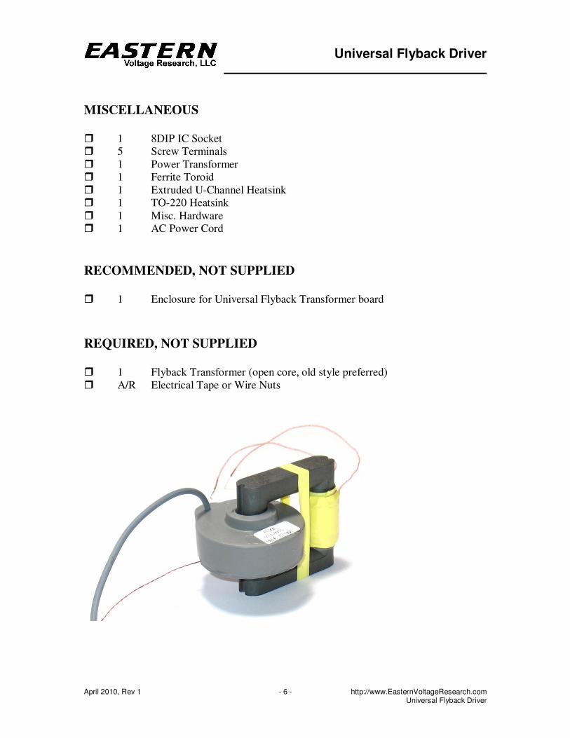
� 1 Flyback Transformer (open core, old style preferred) � A/R Electrical Tape or Wire Nuts
Universal Flyback Driver
April 2010, Rev 1 − 7 − http://www.EasternVoltageResearch.com Universal Flyback Driver
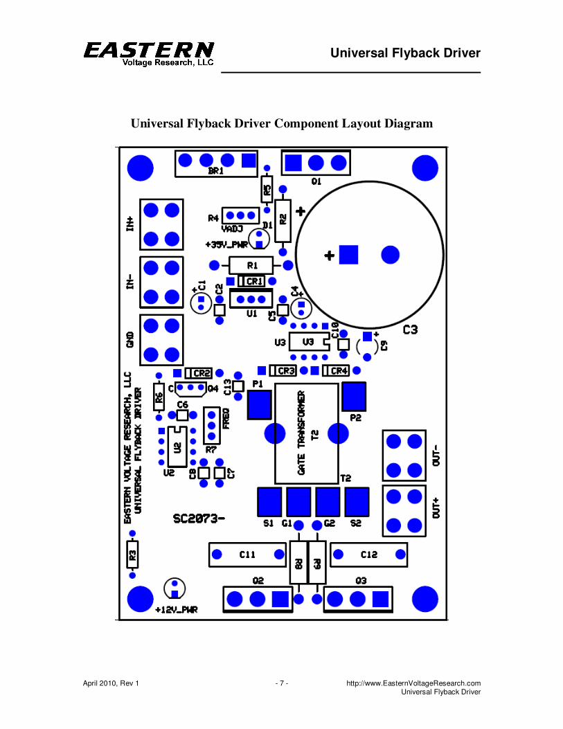
Universal Flyback Driver Component Layout Diagram
Universal Flyback Driver
April 2010, Rev 1 − 8 − http://www.EasternVoltageResearch.com Universal Flyback Driver
KIT Building Instructions
Now we will begin building the kit. There are just a few more important things to know before we install the first components. For each component, the word “install” always means the following: 1. Pick the correct value to start with. 2. Insert the component into the correct printed circuit board (PCB) location. 3. Orient the component correctly – especially when there is a right and a wrong
way to solder it in. (i.e. Electrolytic capacitors, diodes, ICs, transistors, etc…) 4. Solder all connections unless directed otherwise. Ensure enough heat is used to
allow solder to flow for clean, shiny, and completed connections. Also, please be sure to take us seriously when we say that good soldering is the key to the proper operation of your circuit!
• Use a 25W soldering pencil with a clean, sharp tip. DO NOT USE a high power soldering gun such as those trigger activated units.
• Use only rosin core solder intended for electronics use
• Ensure your work area is clean, and has plenty of bright lighting
• Build your kit in stages, taking breaks to check your work. Be sure to clean the board periodically with a brush or compressed air to remove any excess wire cuttings, etc…
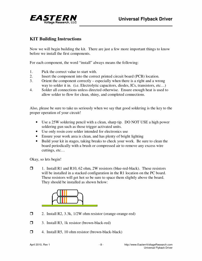
Okay, so lets begin! � 1. Install R1 and R10, 62 ohm, 2W resistors (blue-red-black). These resistors
will be installed in a stacked configuration in the R1 location on the PC board. These resistors will get hot so be sure to space them slightly above the board. They should be installed as shown below:
� 2. Install R2, 3.3k, 1/2W ohm resistor (orange-orange-red) � 3. Install R3, 1k resistor (brown-black-red) � 4. Install R5, 10 ohm resistor (brown-black-black)

Universal Flyback Driver
April 2010, Rev 1 − 9 − http://www.EasternVoltageResearch.com Universal Flyback Driver
� 5. Install R6, 2.2k resistor (red-red-red) � 6. Install R8, 5.1 ohm, 2W resistor (green-brown-gold) � 7. Install R9, 5.1 ohm, 2W resistor (green-brown-gold) � 8. Install CR1, 1N4002 diode. The cathode band on the diode must match that
shown on the silkscreen. � 9. Install CR2, 1N4002 diode. The cathode band on the diode must match that
shown on the silkscreen. � 10. Install CR3, 1N5819 diode. The cathode band on the diode must match that
shown on the silkscreen. � 11. Install CR4, 1N5819 diode. The cathode band on the diode must match that
shown on the silkscreen. � 12. Install C2, 0.1uF capacitor (marking BC104) � 13. Install C5, 0.1uF capacitor (marking BC104) � 14. Install C6, 0.1uF capacitor (marking BC104) � 15. Install C10, 0.1uF capacitor (marking BC104) � 16. Install C7, 2200pF capacitor (marking BC222) � 17. Install C8, 0.01uF capacitor (marking BC103 or M39014/01-1455) � 18. Install C13, 1uF capacitor (marking M39014/02/1407 or BC105) � 19. Install C1, 10uF, 50V electrolytic capacitor. C3 has “polarity.” Polarity
means the capacitor must be inserted a certain way. You may notice that one side of the capacitor, there is a black stripe with minus signs. This is the negative end. Looking at the PCB silkscreen, you will notice the positive side marked. Install this capacitor into the board ensuring the positive side of the capacitor installs in the hole that is marked positive on the PCB layout.
� 20. Install C4, 10uF, 50V electrolytic capacitor. Install this capacitor into the
board ensuring the positive side of the capacitor installs in the hole that is marked positive on the PCB layout.
Universal Flyback Driver
April 2010, Rev 1 − 10 − http://www.EasternVoltageResearch.com Universal Flyback Driver
� 21. Install C9, 10uF, 35V tantalum capacitor (marking 10635). Install this capacitor into the board ensuring the positive side of the capacitor installs in the hole that is marked positive on the PCB layout.
� 22. Install C11, 0.68uF, 250V polypropylene capacitor. � 23. Install C12, 0.68uF, 250V polypropylene capacitor. � 24. Install D1, LED. The short lead of the diode is the cathode and will install
into the square pad on the PCB board. � 25. Install D2, LED. The short lead of the diode is the cathode and will install
into the square pad on the PCB board. � 26. Install an 8-pin DIP socket into the U3 location. Note that one end of the DIP
socket is marked by a notch; this end MUST be oriented as shown on the PCB layout.
� 27. Install U3, UCC37322 Gate Driver IC into the 8-pin DIP socket that was
installed in the previous step. Note that one end of the IC is marked by a dot, notch, or band; this end MUST be oriented as shown on the PCB layout.
� 28. Install U2, 555 Timer. The 555 Timer IC may be soldered directly to the
PCB without worry, but you may use an 8-pin DIP socket (your own) if you prefer. Use the same care in soldering such a socket and inserting the IC as you would in direct soldering of the chip. Note that one end of the IC is marked by a dot, notch, or band; this end MUST be oriented as shown on the PCB layout.
� 29. Install Q4, 2N3904 transistor. This transistor needs to be orientated properly.
Please insert Q4 into the board with the flat edge of the transistor orientated according to the silkscreen layout drawing.
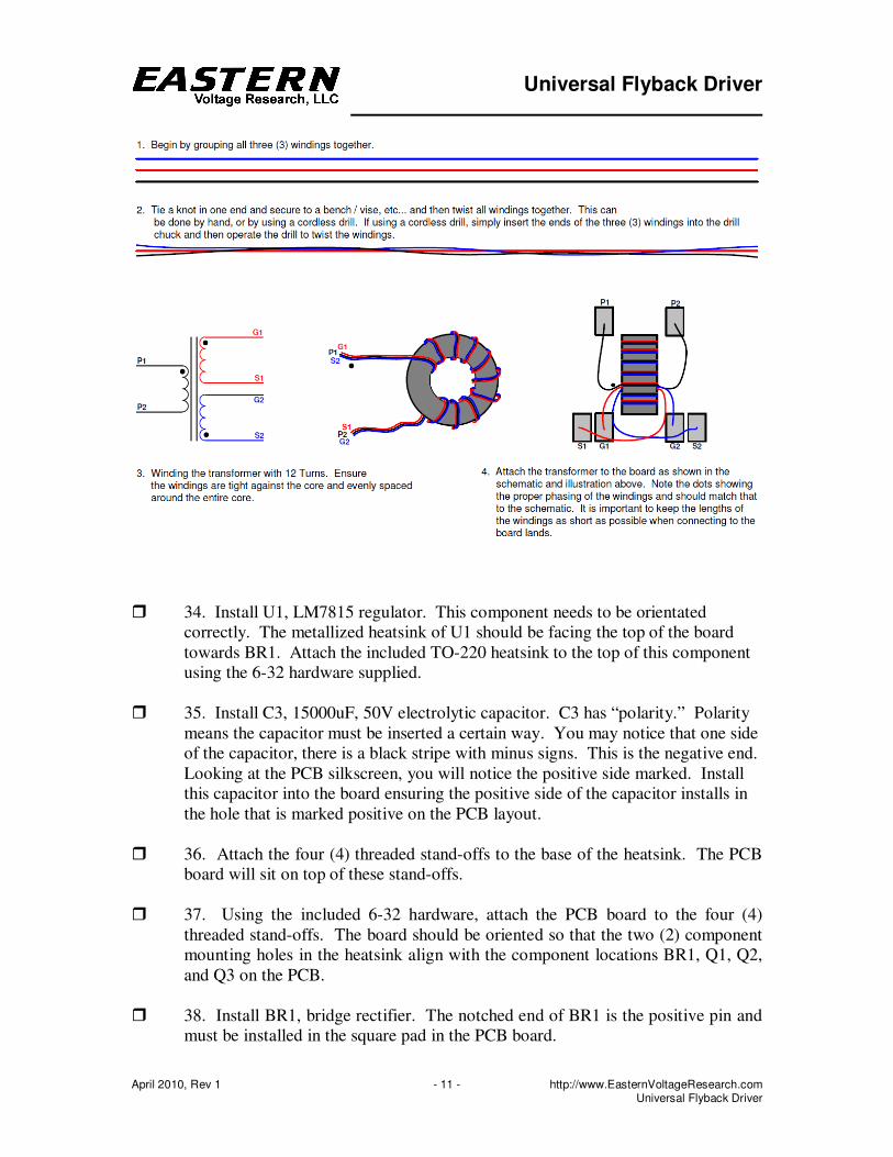
� 30. Install the five (5) screw terminals. � 31. Install R4, 100k potentiometer � 32. Install R7, 100k potentiometer � 33. Build and install T2, gate transformer, as shown in the instructions below.
Visibly check to ensure the windings of the transformer connect to the board as shown below. Failure to connect the windings properly will result in failure of the MOSFET switching devices, Q2 and Q3.
Universal Flyback Driver
April 2010, Rev 1 − 11 − http://www.EasternVoltageResearch.com Universal Flyback Driver
� 34. Install U1, LM7815 regulator. This component needs to be orientated
correctly. The metallized heatsink of U1 should be facing the top of the board towards BR1. Attach the included TO-220 heatsink to the top of this component using the 6-32 hardware supplied.
� 35. Install C3, 15000uF, 50V electrolytic capacitor. C3 has “polarity.” Polarity
means the capacitor must be inserted a certain way. You may notice that one side of the capacitor, there is a black stripe with minus signs. This is the negative end. Looking at the PCB silkscreen, you will notice the positive side marked. Install this capacitor into the board ensuring the positive side of the capacitor installs in the hole that is marked positive on the PCB layout.
� 36. Attach the four (4) threaded stand-offs to the base of the heatsink. The PCB
board will sit on top of these stand-offs. � 37. Using the included 6-32 hardware, attach the PCB board to the four (4)
threaded stand-offs. The board should be oriented so that the two (2) component mounting holes in the heatsink align with the component locations BR1, Q1, Q2, and Q3 on the PCB.
� 38. Install BR1, bridge rectifier. The notched end of BR1 is the positive pin and
must be installed in the square pad in the PCB board.

Universal Flyback Driver
April 2010, Rev 1 − 12 − http://www.EasternVoltageResearch.com Universal Flyback Driver
� 39. Attach the self-adhesive thermal insulator to the heatsink in the position
where Q1 will be mounted. Ensure that the thermal insulator is positioned so that the entire component fits on it. (No overlapping)
� 40. Attach the self-adhesive thermal insulator to the heatsink in the position
where Q2 will be mounted. Ensure that the thermal insulator is positioned so that the entire component fits on it. (No overlapping)
� 41. Attach the self-adhesive thermal insulator to the heatsink in the position
where Q3 will be mounted. Ensure that the thermal insulator is positioned so that the entire component fits on it. (No overlapping)
� 42. Install Q1, IRFP3306 MOSFET. With the PCB board mounted to the
heatsink, first insert Q1 into the board. Do NOT solder Q1 at this time. The metallized back of Q1 will be the side that attaches to the heatsink. Using the included hardware, attach Q1 to the heatsink (ensure the thermal insulator is also in place). Once Q1 is attached to the heatsink, solder it to the board. This ensures that the fit and alignment of Q1 will match the heatsink mounting hole.
� 43. Install Q2, IRFP260 MOSFET. With the PCB board mounted to the heatsink,
first insert Q2 into the board. Do NOT solder Q2 at this time. The metallized back of Q2 will be the side that attaches to the heatsink. Using the included hardware, attach Q2 to the heatsink (ensure the thermal insulator is also in place). Once Q2 is attached to the heatsink, solder it to the board. This ensures that the fit and alignment of Q2 will match the heatsink mounting hole.
� 44. Install Q3, IRFP260 MOSFET. With the PCB board mounted to the heatsink,
first insert Q3 into the board. Do NOT solder Q3 at this time. The metallized back of Q3 will be the side that attaches to the heatsink. Using the included hardware, attach Q3 to the heatsink (ensure the thermal insulator is also in place). Once Q3 is attached to the heatsink, solder it to the board. This ensures that the fit and alignment of Q3 will match the heatsink mounting hole.
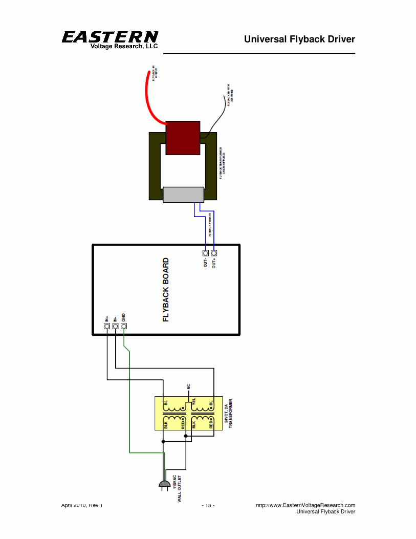
� 45. Install T1, power transformer (and power cord) as shown in the diagram
below. It is very important to attach the ground wire of the AC cord to the GND terminal on the PCB board. Use electrical tape or wirenuts (not supplied) to secure and insulate the connections between the power transformer and AC cord.
DO NOT connect the flyback transformer to the PCB board at this time.
Universal Flyback Driver
April 2010, Rev 1 − 13 − http://www.EasternVoltageResearch.com Universal Flyback Driver
Universal Flyback Driver
April 2010, Rev 1 − 14 − http://www.EasternVoltageResearch.com Universal Flyback Driver
Congratulations! You have just completed your Universal Flyback Driver kit. Please take a few moments to look over the board and ensure that all the components are installed properly with the correct orientation. Since some of the parts may be unfamiliar to you, you may want to be extra sure that they have been inserted correctly. After you are sure that everything seems to be properly installed, move on to the set-up and testing section.
Set-up and Testing
Okay, so lets begin!
RECOMMENDED TEST EQUIPMENT, NOT SUPPLIED
� 1 Analog or Digital Multimeter
Please be sure to wear safety glasses when testing and operating the Universal
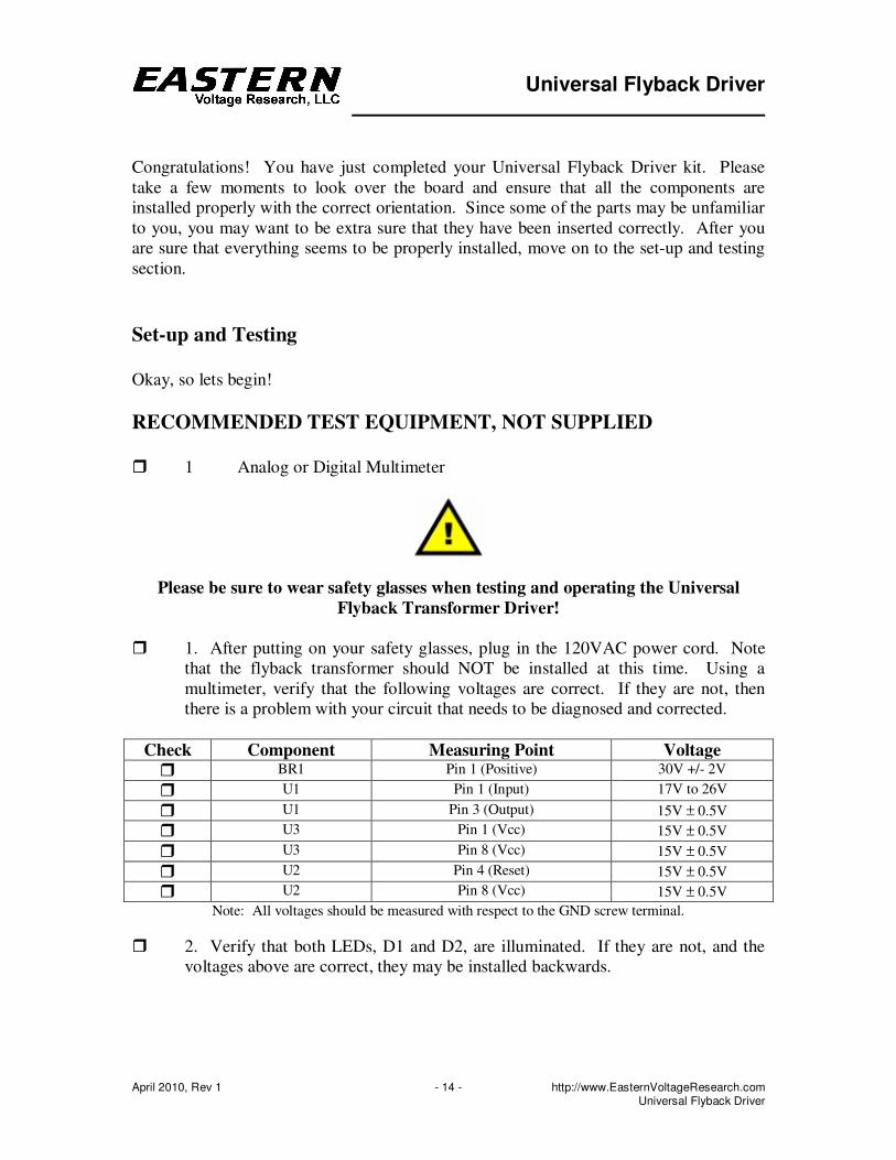
Flyback Transformer Driver! � 1. After putting on your safety glasses, plug in the 120VAC power cord. Note
that the flyback transformer should NOT be installed at this time. Using a multimeter, verify that the following voltages are correct. If they are not, then there is a problem with your circuit that needs to be diagnosed and corrected.
Check Component Measuring Point Voltage
� BR1 Pin 1 (Positive) 30V +/- 2V
� U1 Pin 1 (Input) 17V to 26V
� U1 Pin 3 (Output) 15V ± 0.5V
� U3 Pin 1 (Vcc) 15V ± 0.5V
� U3 Pin 8 (Vcc) 15V ± 0.5V
� U2 Pin 4 (Reset) 15V ± 0.5V
� U2 Pin 8 (Vcc) 15V ± 0.5V
Note: All voltages should be measured with respect to the GND screw terminal.
� 2. Verify that both LEDs, D1 and D2, are illuminated. If they are not, and the voltages above are correct, they may be installed backwards.
Universal Flyback Driver
April 2010, Rev 1 − 15 − http://www.EasternVoltageResearch.com Universal Flyback Driver
� 3. Potentiometer R4 controls the output voltage of Q1 which is the DC bus voltage used to provide power to the half-bridge. Using a multimeter, measure the voltage across Q1-Source to GND and verify that you can adjust this voltage from TBD to TBD volts by adjusting R4. For typical operation, the voltage will be set to its maximum (Q1 saturated and acting as a short). At this time, set the voltage for maximum output voltage. It should be equal to the voltage measured at BR1, Pin 1 in step 1 above.
� 4. Unplug the 120VAC power cord. Due to the capacitor storage on the board, it
may take about 10 seconds for the power to bleed off. Wait until the LEDs completely turn off before proceeding to the next step.
� 5. Install the primary wires of the flyback transformer to the screw terminals
labeled OUT+ and OUT- on the board. � 6. Verify that the ground (RTN)connection from the HV winding of the flyback
transformer is properly connected to GND or some other suitable RTN.
The output of the flyback transformer is High Voltage. DO NOT touch or allow
yourself to come into contact with the output HV wire at any time!
� 8. Plug in the 120VAC power cord. � 9. If everything was installed properly, your flyback transformer should be
operating and producing high voltage. With the power off, you can position the HV output wire close to a GND discharge point to create a high voltage arc.
� 10. Once everything has been verified to be working correctly, you can now try
adjusting the output frequency of your driver. Flyback transformers typically have a resonant frequency between 10kHz and 100kHz depending on their type, size, and configuration. To get maximum output voltage, the output frequency of the driver needs to be set to the resonant frequency of the flyback transformer. To do this, simply adjust potentiometer R7 until the longest output arc is achieved.
Congratulations! Your Universal Flyback Driver is now completed and operational.
Universal Flyback Driver
April 2010, Rev 1 − 16 − http://www.EasternVoltageResearch.com Universal Flyback Driver
Troubleshooting
PROBLEM: No output arc. (Blue LEDs are not working) SOLUTION: In this case, either Q1, Q2, Q3 or U3 has probably failed. Your unit will require diagnose and repair. PROBLEM: Output arc is very small SOLUTION: The output frequency of the driver may not be set correctly. Try adjusting potentiometer R7 to try to match the output frequency of the driver to the resonant frequency of the flyback driver. Also, ensure that the voltage output of Q1 is set at its maximum voltage. Potentiometer R4 is used to adjust this output voltage.
Conclusion We sincerely hope that you have enjoyed the construction of this Eastern Voltage Research Kit. As always, we have tried to write this instruction manual in the easiest, most “user friendly” format that is possible. As our customers, we value your opinions, comments, and additions that you would like to see in future publications. Please submit comments or ideas to: Eastern Voltage Research, LLC Technical Support [email protected] Thanks again from the people here at Eastern Voltage Research.
Universal Flyback Driver
April 2010, Rev 1 − 17 − http://www.EasternVoltageResearch.com Universal Flyback Driver
Terms and Conditions of Sale
Privacy
We do not provide any information to anyone for any reason.
Shipping
We will make every attempt to ship all orders received within 48 hours of order receipt with the exception of custom ordered components and / or kits. This excludes weekends and holidays. Regular ground service is handled via USPS or UPS. Backorders - all partial shipment backorders will be shipped via regular ground service at our expense.
International Orders
All foreign orders are shipped via USPS International Priority service unless otherwise noted. You are wholly responsible for any custom duties, brokerage fees, import restrictions, etc... that are imposed after the sale.
Order Cancellations
Before you submit your order, please make sure you really want it. Once we have begun processing an order, a 25% restocking fee will be applied, prior to any refund. If you do not agree with this policy, please do not order.
Legal Status of Products
It is the responsibility of the Buyer (not Eastern Voltage Research, LLC) to ascertain and obey all applicable local, state, and federal laws in regard to the possession and the use of any item or kit that is offered for sale. Consult your attorney regarding local, state, and federal laws prior to ordering. By placing an order, the buyer represents that he / she is of legal age and that the products will be used
only in a lawful manner.
Electronics Kit Limit of Liability
Our range of electronics kits are intended for educational and demonstration purposes only. They are not intended for use in commercial applications. If they are used in such applications, the purchaser assumes all responsibility for ensuring compliance with
local laws. When a product is supplied in kit form and assembly or construction has commenced or the inner component packages have been opened, we are unable to offer any form of refund, replacement, exchange, or free repair. This is because we cannot guarantee the labor you provide and components can be damaged during assembly. Component packages should be checked against
the components list supplied and any shortages or damaged components must be advised to us within 7 days of delivery date to ensure free component replacement.
It is recommended that if a kit builder does not have enough knowledge to diagnose faults, that the project should not be started unless assistance can be obtained. (Unfortunately, an improperly installed component or bad solder joint or wiring mistake can take many
hours to diagnose and at normal service rates, the service charge could well be more than the total cost of the electronics kit.)
Mains Powered Projects
To ensure your safety, please observe these safety measures. In no way are these complete. As safety requirements vary, please check with your local authorities, in order to comply with local requirements. If in doubt, seek the help of a qualified person.
Due to their nature and function, some electronics kits require MAINS power (115VAC) to be connected directly to the Printed
Circuit Board (PCB). Extreme care should be taken when assembling and testing these kits. MAINS power must be treated very carefully. It is strongly recommended that you have previous experience of working with MAINS power equipment and / or circuits prior to attempting assembly of these kits. MAINS power can cause serious injury or death and must therefore be treated with extreme
CAUTION. Construction, testing, and use of these kits should only be attempted by competent persons, and / or under the supervision of someone fully experienced in this field.
To ensure electrical safety, and also protection from fire or personal injury, make sure your MAINS operated equipment complies with the safety recommendations below:
- Use a suitable non-conductive enclosure (wood, plastic, etc...) If you use a metal enclosure, be sure that the enclosure is
properly grounded to earth ground. - Use a power switch for any device that consumes more than 10W of power. A double throw switch should be utilized for MAINS operated, transformer-less connections.
- A fuse should be utilized in series with the MAINS switch. - Use a suitable MAINS input connector, and / or a UL three-conductor power cord which is clamped to your enclosure. - Use properly insulated and sized wire when making any MAINS power connections inside an enclosure.
We accept no responsibility for injury, loss, or damage of any kind as a result of the purchase, assembly, or use of any of our products.
Limitation of Liability
The Customer will be responsible for ensuring the fitness for purpose of the Goods for the Customer's application. Eastern Voltage
Research, LLC accepts no liability whatsoever or howsoever arising in respect to loss, damage, or expense arising from errors in information, or advice provided whether or not due to Eastern Voltage Research, LLC's negligence or that of its employees, agents, or sub-contractors save for any loss or damage arising from personal injury. Eastern Voltage Research, LLC shall not be liable to the
Customer by reason of any representation (unless fraudulent), or any implied warranty, condition or other term, or any duty at
Universal Flyback Driver
April 2010, Rev 1 − 18 − http://www.EasternVoltageResearch.com Universal Flyback Driver
common law, or under express terms of Contract with the Customer, for any indirect, special, or consequential loss or damage (whether for loss of profit or otherwise), costs, expenses, or other claims for compensation whatsoever (whether cause by the negligence of Eastern Voltage Research, LLC, its employees or agents or otherwise) which arise out of or in connection with the
supply of the Goods or their use or resale by the Customer. The entire liability of Eastern Voltage Research, LLC under or in connection with the Contract with the Customer shall not exceed the price of the Goods except as expressly provided in these Terms and Conditions of Sale.
Parts Substitutions
Eastern Voltage Research, LLC reserves the right to substitute components in all electronics kits offered provided that the functional performance of a kit is not diminished in any way.
Miscellaneous
Prices are subject to change. Product styles and parts lists may vary. New Jersey orders must add 7% sales tax. If tax exempt, please
include a resale certificate. We assume no liability associated with product usage. The buyer is liable and responsible for any loss, damage, or expense of any kind, arising out of the use or misuse of the products. By placing an order, the buyer signifies agreement to these Terms and Conditions of Sale.
Warranty Information
Defective Components
Its always easy to blame a component for a problem with your kit. Before you conclude that a component may be defective, please thoroughly check your work. Today's semiconductors and passive components have reached incredibly high reliability levels, and its
sad to say that our human construction skills have not! However, on rare occasions, components which are defective may be shipped and included in your kit. All of our kit parts carry the Eastern Voltage Research, LLC Warranty that they are free from defects for a full ninety (90) days from the date purchase with the exception of power semiconductors (see below). Defective parts will be replaced promptly at our expense. If you suspect a component to be defective, please mail it to us for testing and replacement. Please send only
the defective component(s), not the entire kit. The component(s) MUST be returned to us in suitable condition for testing. Please be aware that testing can usually determine if the part was truly defective or damaged by assembly and / or usage. If you did damage or "blow-up" a component through testing, don't be afraid to tell us. We're all human and in most cases, replacement parts are very
reasonably priced.
Power Semiconductors
Due to the nature of the kits, we cannot offer any warranty or replacement for defective or damaged power semiconductor components. This includes both MOSFETs and IGBTs. That said, all power semiconductors are thoroughly tested prior to shipment to
ensure that you have a power semiconductor that is non-defective and in NEW, unused condition.
Missing Parts
Before assuming that a component value is incorrect, or missing, check the parts listing carefully to see if it is a critical value such as a specific semiconductor or IC, or whether a RANGE of values is suitable (such as "10uF to 47uF"). Sometimes, a different value
component may be substituted in a non-critical application. Eastern Voltage Research, LLC electronics kits are assembled and packed with pride in the USA. If you believe we packed an incorrect part or omitted a component clearly indicated in your instruction manual as supplied, please contact us with information on the component so we can send a replacement as soon as possible.
Factory Repair of Assembled Kits
In the event you are having difficulty with your kit and need assistance, we do offer a factory repair service. However, to qualify for an Eastern Voltage Research, LLC factory repair, electronics kit MUST:
- NOT be assembled with acid core solder or flux - NOT be modified in any manner
- BE returned in full-assembled form. Kits partially assembled will not be accepted and you will lose your repair deposit. - BE accompanied by the proper repair fee. No repair will be initiated until we have receive the MINIMUM repair fee (1/2 hour labor) of $20.00.
- INCLUDE a written description of the particular problem and legible return address inside the SAME shipping carton. Please do not include your own hardware such as non-Eastern Voltage Research power supplies, transformers, batteries, cables, etc... Eastern Voltage Research, LLC, reserves the right to refuse repair on ANY item in which we find excessive
problems or damage due to construction methods. To assist customers in such situations, Eastern Voltage Research, LLC, reserves the right to solve their needs on a case-by-case basis.
The cost of repair for any kit is $40.00 per hour, regardless of the cost of the kit. Please understand that our technicians are not volunteers and that set-up, testing, diagnosis, repair, and repacking and paperwork can take nearly an hour of paid employee time even on a simple kit. Of course, if we find a component that was defective in manufacturer, there will be no charge to the repair of your kit.
(But please realize that our technicians know the difference between a defective component and parts burned out or damaged through improper use or assembly.)

Universal Flyback Driver
April 2010, Rev 1 − 19 − http://www.EasternVoltageResearch.com Universal Flyback Driver
Electronics Kit Return Policy
If you feel, for any reason, that you will have difficulty building any kit-based product purchased from us (and you cannot get assistance from a friend), you can return it for a refund (minus shipping costs) provided a Return Authorization (RA) number is obtained first from us by email. The items must be returned to use (insured against damage in transit) at the customer's expense and
received by us in original condition (with all product packaging, documentation, and a copy of the original sales invoice) within 14 days of original invoice date. The RA number must be clearly stated on the shipping carton. Kits may not be returned for any form of refund or credit once the inner component packages have been opened or construction has been started.
Components Return Policy
Individually purchased components may not be returned for any reason. If you do not agree with this policy, please do not order.