Embed Size (px)
Citation preview

Instruction Enhancement Programme(IEP)
on
Introduction to Analog and
Digital VLSI Design
LAB MANUAL FOR ANALOG LAB-II
Department of Electronics and Electrical Engineering
Indian Institute of Technology Guwahati.

Current Mirrors
Aim: Analysis and simulation of various current mirror configuration.
Parameters: 1. TSMC 180nm technology.
2. L=200nm and W= 400nm.
3. μnCOX = 300 μA/V2
4. Vth = 0.5 V.
5. Minimum VDS = 0.2V.
6. λ = 0.45.
Basic Current Mirror Circuit
Circuit Diagram:

Steps to design and simulate basic current mirror circuit with given
parameters:
1. To calculate the IREF:
𝐼 = 1
2 𝜇𝑛 𝐶𝑂𝑋
𝑊
𝐿 (𝑉𝐺𝑆 − 𝑉𝑡ℎ)2
Now, using the given parameters and assuming 𝑉𝐺𝑆 − 𝑉𝑡ℎ= 0.2 V, current
should be:
I = 12 μA.
2. Now, set the voltage source (V1) for MOS (MN2) as 0.2V, or if one wants
to put V1= 1.8V then put a resistor of 133KΩ to ensure a minimum of 0.2V
across VDS.
3. Once the component values finalized then proceed to setup for simulation.
We will perform the operating point simulation, the method to set the same
can be seen in following figure:
4. Also, TSMC 180nm technology file have to be included. Technology file
can be find in $ADK/technology/ic/models/tsmc018.mod and included as
shown in following figure:

5. Now, Run the simulation and observe the Currents in MOS MN1 and MN2.

Study the variation of VDS and IREF on basic current mirror circuit:
1. To study the variation of VDS on the basic current mirror circuit, we have to
perform a DC-sweep analysis of V1 for a voltage range (0 to 1.8V with
0.001V step). The setup for DC-sweep analysis is shown in following figure:
2. Now, run the simulation and plot the ID2 Vs VDS using Ezwave plotting tool
as shown in figure:

3. Similarly, the variation with IREF can be studied.
Assignments:
1. Change the W/L by some factor (double, triple etc) for MOS MN2 and
observe the change in current.
2. Also, multi-finger configuration should be studied.
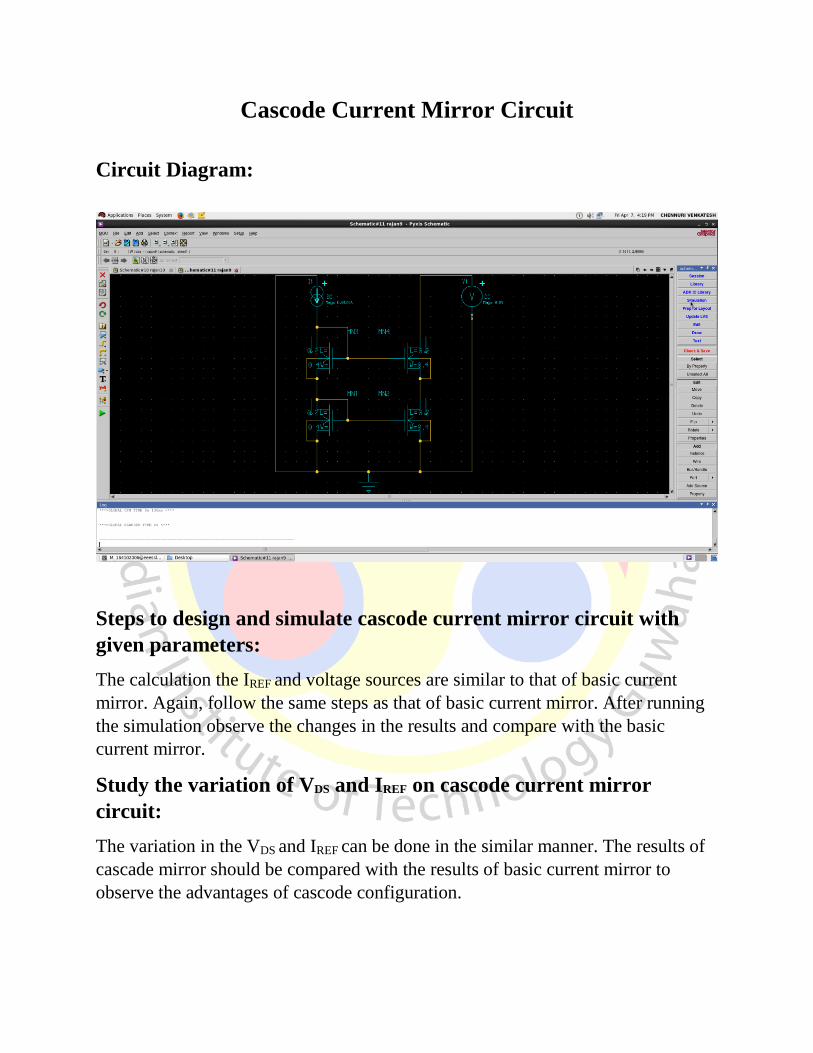
Cascode Current Mirror Circuit
Circuit Diagram:
Steps to design and simulate cascode current mirror circuit with
given parameters:
The calculation the IREF and voltage sources are similar to that of basic current
mirror. Again, follow the same steps as that of basic current mirror. After running
the simulation observe the changes in the results and compare with the basic
current mirror.
Study the variation of VDS and IREF on cascode current mirror
circuit:
The variation in the VDS and IREF can be done in the similar manner. The results of
cascade mirror should be compared with the results of basic current mirror to
observe the advantages of cascode configuration.

Self-bias cascode current mirror circuit
Circuit Diagram:

Steps to design and simulate cascode current mirror circuit with
given parameters:
1. To calculate the IREF:
𝐼 = 1
2 𝜇𝑛 𝐶𝑂𝑋
𝑊
𝐿 (𝑉𝐺𝑆 − 𝑉𝑡ℎ)2
Now, using the given parameters and assuming 𝑉𝐺𝑆 − 𝑉𝑡ℎ= 0.2 V, current
should be:
I = 12 μA.
2. To calculate R:
𝑅 = 𝑉𝑂𝑉
𝐼 =
0.2 𝑉
12 μ𝐴= 16.66 KΩ.
3. The minimum VDS or V1 should be 0.4V.
Study the variation of VDS and IREF on basic current mirror circuit:
1. To study the variation of VDS on the self bias cascode current mirror circuit,
we have to perform a DC-sweep analysis of V1 for a voltage range (0 to
1.8V with 0.001V step).
2. Now, run the simulation and plot the ID2 Vs VDS using Ezwave plotting tool:
3. Similarly, the variation with IREF can be studied.
Differential Amplifier with cascode current
mirror as load
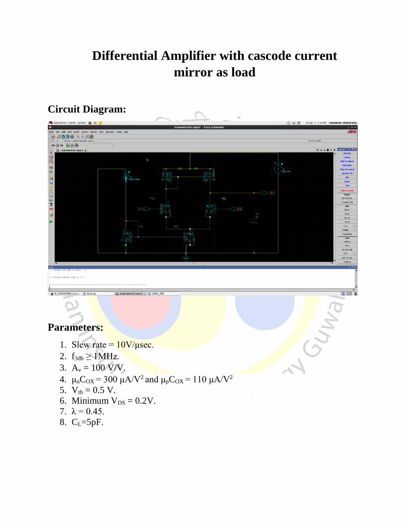
Circuit Diagram:
Parameters:
1. Slew rate = 10V/μsec.
2. f3db ≥ 1MHz.
3. Av = 100 V/V.
4. μnCOX = 300 μA/V2 and μpCOX = 110 μA/V2
5. Vth = 0.5 V.
6. Minimum VDS = 0.2V.
7. λ = 0.45.
8. CL=5pF.

Steps to design and simulate Differential Amplifier with cascode
current mirror as load:
1. From the Slew rate which is given as 10V/μsec:
𝑆𝑙𝑒𝑤 𝑟𝑎𝑡𝑒 = 𝐼𝑆𝑆
𝐶𝐿=
𝐼𝑆𝑆
5𝑝𝐹= 10V/μsec
𝐼𝑆𝑆 ≥ 50 𝜇𝐴.
2. Now, from the cut-off criteria given i.e. f3db ≥ 1MHz:
1
2𝜋𝑅𝐶≥ 1𝑀𝐻𝑧
Hence,
𝑅 ≤ 31.83 𝐾𝛺
3. Again from the output resistance of circuit:
𝑅𝑂𝑈𝑇 = 2
(𝜆𝑛 + 𝜆𝑝)𝐼𝑆𝑆
Therefore,
𝐼𝑆𝑆 ≥ 70 𝜇𝐴
Now, from steps 2 and 3, assuming current to be 100 𝜇𝐴.
4. Sizing of PMOS:
The current from PMOS = 50 μA and assume minimum VDS of 0.2V, hence
W/L can be estimated from the equation of current as:
𝑊
𝐿= 22.72
Since, L=0.2 μm, therefore W=4.54μm.

5. The Sizing of NMOS can be determined from the Gain criteria:
𝐴𝑉 = 𝑔𝑚 𝑅𝑂𝑈𝑇
𝑊
𝐿= 25.98
Since, L=0.2 μm, therefore W=5.196μm.
6. Similarly, the sizing of MOS in the mirror circuit can be evaluated:
𝑊
𝐿= 50/3
Since, L=0.2 μm, therefore W=10/3μm.
7. Once the designing part is over proceed for simulation setup and apply the
dc bias and small signal to input MOSFETs. Also, for this circuit we will
perform ac analysis. The steps for simulation setup is shown in figure below:


8. After the simulation plot the Gain Vs Frequency using Ezwave utility.