Embed Size (px)
Citation preview
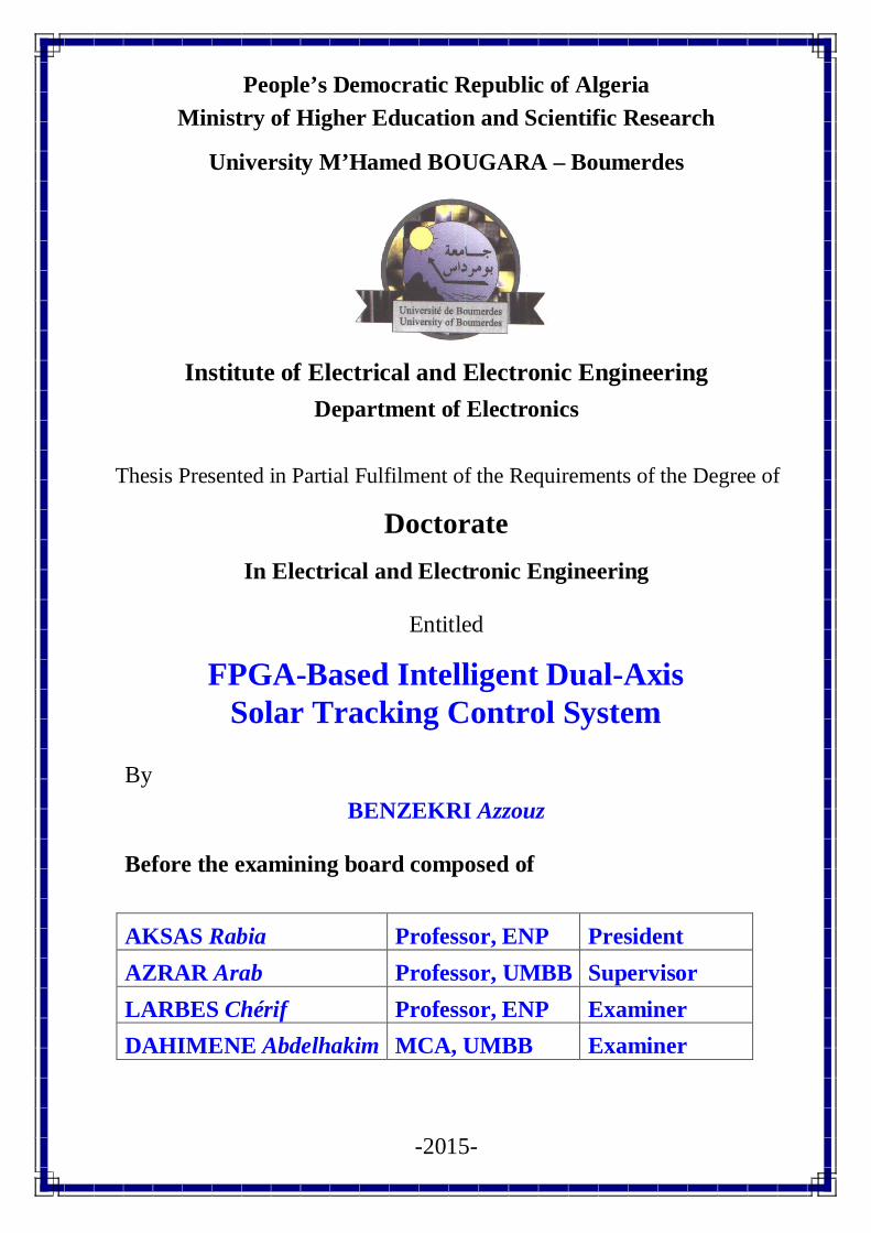
-2015-
People’s Democratic Republic of Algeria Ministry of Higher Education and Scientific Research
University M’Hamed BOUGARA – Boumerdes
Institute of Electrical and Electronic Engineering
Department of Electronics
Thesis Presented in Partial Fulfilment of the Requirements of the Degree of
Doctorate In Electrical and Electronic Engineering
Entitled
By BENZEKRI Azzouz
Before the examining board composed of AKSAS Rabia Professor, ENP President AZRAR Arab Professor, UMBB Supervisor cccc LARBES Chérif Professor, ENP Examiner DAHIMENE Abdelhakim MCA, UMBB Examiner
FPGA-Based Intelligent Dual-Axis Solar Tracking Control System

Acknowledgments Acknowledgments
i
Acknowledgments
I express my sincere gratitude to my supervisor Professor Arab
AZRAR for allowing me to conduct this research under his auspices
despite his busy agenda. I am especially grateful for his
confidence, the freedom he gave me to do this work, his assistance,
support and encouragements throughout the course of this work.
I am deeply grateful to Professor Rabia. AKSAS for agreeing to chair
the jury. My warmest thanks go to Professor Cherif. LARBES and
Dr Abdelhakim DAHIMENE for accepting to participate in the
defense of this thesis.
I am grateful to Amira for her support and kindness.
Abstract Abstract
ii
Abstract
This thesis describes the design process of an FPGA-based sensor-driven
intelligent controller applied to a dual-axis sun tracking system. Fuzzy
control based on fuzzy logic theory is used as a solution for the FPGA
implementation of a digital controller for this industrial application. The
real-time controller determines when and how much to tune the driving
motors to minimize the misalignment of the solar panel surface with the sun’s
incident rays during the day in order to harvest maximum power from the
solar panel mounted on a tracker.
To achieve such a digital controller, we developed an FPGA-based
heterogeneous computing platform with the capability of partitioning the
overall controller between two concurrent subsystems: (1) a hardware
subsystem made up of a pair of fuzzy-like PD-type controllers implemented
on the programmable fabric of the FPGA using the (Very-High Speed
Integrated Circuit) Hardware Description Language (VHDL), and (2) a
software subsystem, a soft processor Nios® II-based supervisory control
system implemented using the system-on-a-programmable (SoPC) approach.
This hardware/software codesign implemented in a single chip makes the
connections between the two subsystems work with low power and low
latency resulting in an optimal efficiency and performance.
Abstract Abstract
iii
An experimental structure is constructed in the laboratory. The controller
allows this structure to perform an approximate three-dimensional
hemispheroidal rotation to track the sun’s movement during the day to
improve the overall efficiency of the solar panel.
Integrating the whole digital controller in a single chip accelerates
development time while maintaining design flexibility. Moreover, it reduces
the circuit board costs with a single-chip solution, and simplifies product
testing. Compared with traditional design approach using programmed logic
(microprocessor- microcontroller- and DSP-based systems), the proposed
solution uses a single low-cost FPGA device while enabling higher degrees of
flexibility and concurrency.
The digital controller developed with Altera Quartus II 9.1 sp2 Web
Edition software development suite tools is simulated and realized on a
Cyclone-II EP2C35F672C6 FPGA platform to verify its feasibility and
functionality.
Keywords: FPGA; SoPC; Fuzzy logic module; Nios® II; Sun tracker.

Abstract Abstract
iv
)FPGA (.
.
)FPGA (
: (1)
)FPGA( VHDL (2) «Nios® II »
)SoPC. ( )Quartus II (
)Altera (
.
)FPGA( )Cyclone II EP2C35)
.
Nios® II SoPC FPGA :
Résumé Résumé
iv
Résumé
Cette thèse décrit le processus de conception d'un contrôleur intelligent à base de
FPGA appliqué à un système de poursuite du soleil à double axe. Le contrôleur a base de
logique floue détermine en temps réel quand et de combien faudrait-il ajuster les moteurs
d'entraînement pour minimiser le désalignement de la surface du panneau solaire avec les
rayons du soleil pendant la journée afin de récolter le maximum de puissance du panneau
solaire monté sur un suiveur.
Pour atteindre un tel objectif de commande numérique, nous avons développé une
plate-forme informatique hétérogène à base de FPGA avec la possibilité de cloisonner le
contrôleur global entre deux sous-systèmes simultanés: (1) un sous-système de matériel
informatique constitué d'une paire de logique floue comme régulateurs de type PD mis en
œuvre sur FPGA en utilisant le langage VHDL, et (2) un système de contrôle de
surveillance à base II processeur Nios® mis en œuvre en utilisant l’approche SoPC. Cette
conception matériel / logiciel mise en œuvre dans une seule puce rend les connexions entre
les deux sous-systèmes fonctionnent avec une faible puissance et de faible latence résultant
en une efficacité et des performances optimales.
L’intégration du contrôleur numérique en une seule puce accélère le temps de
développement tout en maintenant la flexibilité de conception. En outre, il réduit les coûts
avec une solution mono-puce, et simplifie les tests de produits. Par rapport à l'approche
traditionnelle de conception utilisant la logique programmée (microprocesseur et
microcontrôleur et de DSP), la solution proposée utilise un dispositif de FPGA à faible coût
unique tout en permettant des degrés de flexibilité et de concurrence plus élevés.
Le contrôleur numérique développé avec le logiciel de développement d’Altera le
Quartus II Edition 9.1 sp2 est simulé et réalisé sur une plate-forme Cyclone II FPGA
EP2C35F672C6 pour vérifier sa faisabilité et sa fonctionnalité.
Mots Clés: FPGA; SoPC; Logique Floue; Nios® II; Suiveur.
v
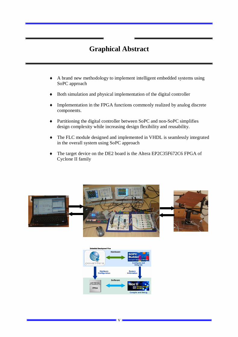
Graphical Abstract
A brand new methodology to implement intelligent embedded systems using SoPC approach
Both simulation and physical implementation of the digital controller
Implementation in the FPGA functions commonly realized by analog discrete components.
Partitioning the digital controller between SoPC and non-SoPC simplifies design complexity while increasing design flexibility and reusability.
The FLC module designed and implemented in VHDL is seamlessly integrated in the overall system using SoPC approach
The target device on the DE2 board is the Altera EP2C35F672C6 FPGA of Cyclone II family

Table of Contents Table of Contents
vi
Table of Contents
Acknowledgement…………………………………………………………………....i
Abstract……………………………………………………………………………....ii
Graphical Abstract……………...…………………………………………………....v
Table of Contents………………………………………….........................................vi
List of Figures……………………………………………………………………..…xi
List of Tables………………………………………………………………………..xiv
List of Abbreviations………………………………………………………………..xiv
Chapter 1 Introduction_____________________________________
1 Introduction………………………………………………………………….1
2 Renewable Energies………………………………………………………....2
2.1 Hydro source of Energy……………………………………………....2
2.2 Wind Source of Energy………………………………………………3
2.3 Biomass Source of Energy…………………………………………...3
2.4 Geothermal Source of Energy………………………………………..3
2.5 Solar Energy………………………………………………………….3
3 Sun Tracker Types …………………………………………………………5
4 Sun Tracker Driving Modes……………………………………………….6
5 Computing Platforms………………………………………………………7
5.1 ASIC Solution………………………………………………………..7
5.2 Software-Programmed Logic………………………………………...8
5.3 Reconfigurable Logic or Programmable Hardware………………….8
Table of Contents Table of Contents
vii
5.4 Implementation of Fuzzy Controllers…………….………………….9
6 Structure of the Sun Tracking System………………..…………………..10
7 Objectives of the Thesis…………………………………………………....11
8 Organization of the Thesis………………………………………………...13
Chapter 2 Literature Review________________________________
1 Introduction………………………………………………………………....14
2 Open Loop Tracking Strategies….…………………………………….…..15
3 Closed Loop Tracking Strategies….………….…………………….….…..18
4 FPGA Based Tracking Strategies….……………………………….….…..21
5 Fuzzy Control Tracking Strategies….…………………………….….…...24
Chapter 3 Fuzzy Logic_____________________________________
1 Introduction………………………………………………………………...26
2 Fuzzy Sets……..…………………………………………………………….27
2.1 Operations with Fuzzy Sets………………………………………….28
2.2 Properties of Fuzzy Sets………………………..................................30
3 Membership Functions…………………………………………………......32
3.1 Piecewise Linear Membership Function……………….....................33
3.1.1 Triangular Membership Function…….………..........................33
3.1.2 Trapezoidal Membership Function………….............................33
3.2 Features of the Membership Function……….....................................34
3.2.1 Core…………………………………… ………………………34
3.2.2 Support…..….………………………………... ………………34
3.2.3 Boundary..……..……………………………………………….34
3.2.4 Height…..……..…......................................................................34
3.3 Structure of Membership Functions…………………………………35
Table of Contents Table of Contents
viii
3.4 Number and Degree of Overlapping of Membership Functions…….36
3.5 Linguistic Variables and Values……………......................................36
4 Fuzzy IF-THEN Rules……………………………………………… …...….37
5 Properties of Fuzzy Rules………………………………………...................38
5.1 Completeness………………………………………………………..39
5.2 Consistency………………………………………………………….39
5.3 Continuity…………………………………………………………....40
6 Fuzzy Logic Controller……………...….........................................................40
6.1 Fuzzification Interface………………………………........................ 41
6.2 Fuzzy Knowledge Base……………………………...........................41
6.3 Fuzzy Inference Mechanism…………………………………………42
6.3.1 Fuzzy Implication…………………….......................................42
6.3.2 Aggregation of Fuzzy Conclusions……………………….........43
6.4 Defuzzification Interface……………….............................................45
6.4.1 Maxima Methods........................................................................46
6.4.1.1 First of Maxima (FOM)……………………………...46
6.4.1.2 Last of Maxima (LOM)……………………………....47
6.4.1.3 Middle of Maxima (MOM)…………………………..47
6.4.2 Distribution Methods…………………………………………..47
6.4.2.1 Max-Membership Method……………….……….......48
6.4.2.2 Weighted Average Method……………….…..............48
6.4.2.3 Center of Gravity (COG)…………… ……….………49
6.4.2.4 Center of Gravity for Singleton (COGS)……. ….…...49
Chapter 4 FPGA Technology_______________________________
1 Introduction………………………………………………………………..51
2 History and Evolution of Programmable Logic devices…………………52
3 Architecture of FPGAs…………………………………………………….54
3.1 Logic Element……………………………………………………….55
3.2 Logic Array Block…………………………………………………...55
Table of Contents Table of Contents
ix
3.3 Adaptive Logic Module……………………………………………..56
. 3.4 Integrated Functional Blocks…………………………..……………57
3.4.1 Embedded RAM Blocks………………………………………57
3.4.2 Embedded Multiplier Blocks………………………………….58
3.4.3 Gigabit Transceivers………………………………………......60
3.4.4 Embedded Processor Cores……………………………………60
4 FPGA Programming Technologies……………………………………….……..61
4.1 SRAM-Based FPGA……………………………………………..….61
4.2 Antifuse-Based FPGA……………….…………………………….. .61
4.3 Flash-Based FPGA…………………...……………………………. .61
5 Applications of FPGAs………………………………..….……………………...62
6 The Nios® II and SoPC Builder…………………………………………………62
6.1 The Nios® II Processor……………………………………………...62
6.2 The SoPC Builder…………………………………………………....65
Chapter 5 Design of the Fuzzy Logic Module__________________
1 Introduction………………………………………………………………...68
2 Structure of the Fuzzy Logic Module…………………………………......69
3 Fuzzy Logic Controller Design Flow……………………………………...69
4 The Azimuth Fuzzy Logic Controller…………………………………….71
4.1 Input/Output Membership Functions………………………………..72
4.2 Construction of Rule Base…………………………………………..74
5 The Elevation Fuzzy Logic Controller……………………………………77
Chapter 6 Hardware/Software Codesign Implementation_________
1 Introduction………………………………………………………………...79
2 FPGA Hardware Design Flow (SoPC Approach)………… …………….80
3 Implementation of the Intelligent Sun Tracking Controller…………….82
Table of Contents Table of Contents
x
3.1 Off-Chip Hardware Module……………………………….………...83
3.1.1 Sun Finder Unit………………………………………..............83
3.1.2 Data Acquisition Unit…………………………………………85
3.1.3 Bidirectional Voltage Level Translation Unit……………… ..88
3.1.4 Motors Driving Unit…………………………………………..88
3.2 On-Chip Hardware Module………………………………………….91
3.2.1 On-Chip non-SoPC Builder Subsystem……………………….91
3.2.1.1 The clock divider module…………………………....91
3.2.1.2 Implementation of the Fuzzy Logic Module...……....92
3.2.1.3 Stepper Motor Sequence Generator………………….93
3.2.2 On-chip SoPC Builder Subsystem………………….………....95
3.2.3 Building the Embedded System in the SoPC Builder……..….96
3.2.4 Integrating the SoPC and non-SoPC Builder…………………..
Subsystems in Quartus II Project…………………………….99
3.2.5 Firmware Development……..…………………………….. ...101
4 Real-Time Experiment……………………………………………………102
4.1 Operational Cycle Time…………………………………………….103
4.2 Simulation…………………………………………………………..104
Chapter 7 Conclusions………………………………………………………106
References……………………………………………………………………………….109
List of Figures List of Figures
xi
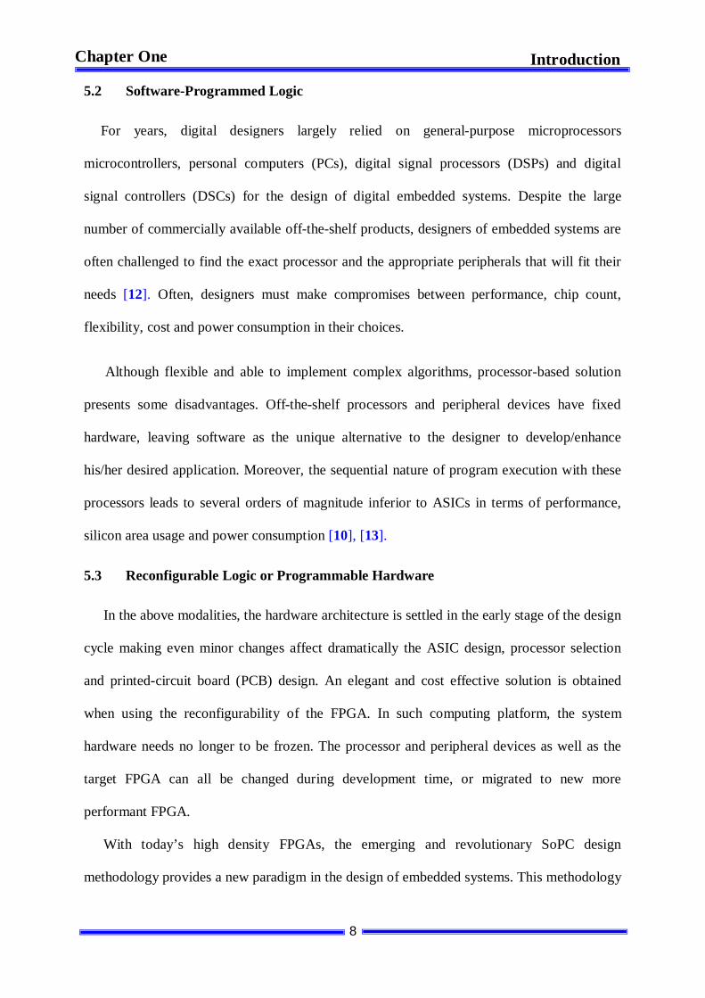
List of Figures Figure-1.1 (left) A dam to energize a hydroelectric power station. (right) Airflows……..
used to run wind turbines……………………………………………………...2
Figure-1.2 Wood chip bio fuel a renewable alternative source of energy…………………3
Figure-1.3 (a) Multi-crystalline-based solar panel. (b) Single crystal-based solar panel.
(c) Amorphous-based solar panel……………………………………………....4
Figure 1.4 Structure of a dual-axis sun tracker…………………………………………….6
Figure-1.5 High-level representation of the FPGA-based intelligent dual-axis sun
tracking system………………………………………………………………..10
Figure-1.6 Pictorial representation of the FPGA-based intelligent dual-axis sun…………
Tracking system……..………………………………………………………...12
Figure-3.1 Membership function for crisp and fuzzy sets………………………………..27
Figure-3.2 Graphical representation of complement, union and intersection ……………
of fuzzy operations…………………………………………………………....29
Figure-3.3 Graphical representation of fuzzy union and intersection…………………….30
Figure-3.4 Fuzzy membership function for speed………………………………………..32
Figure-3.5 Asymmetric triangular and trapezoidal membership functions…………….…33
Figure-3.6 Features of a membership function…………………………………………...34
Figure-3.7 Graphical representation of a fuzzy variable with 5 fuzzy sets……………….35
Figure-3.8 Structure of a generic Mamdani type Fuzzy Logic Controller…………….….41
Figure-3.9 Graphical representation of Max-Min and Max-Prod inference………………
List of Figures List of Figures
xii
methods with crisp inputs with two inputs and two rules………………….…44
Figure-3.10 Example of defuzzification for two-rule fuzzy inference…………………….45
Figure-3.11 First, Last and Middle of maxima defuzzification methods………………….47
Figure-3.12 Max-membership defuzzification method……………………………………48
Figure-3.13 Weighted average defuzzification method…………………………………...48
Figure-4.1 Generic structure of a CPLD…………………………………………………53
Figure-4.2 Generic structure of an early FPGA………………………………………….54
Figure-4.3 Block diagram of the Altera logic element…………………………………...55
Figure-4.4 Block diagram of a Cyclone II LAB [78]…………………………………….56
Figure-4.5 High-level block diagram of the Altera Stratix-V ALM [79]…………….…..57
Figure-4.6 An M4K RAM embedded memory block in a Cyclone FPGA [78]…………58
Figure-4.7 Architecture of an embedded multiplier block in a Cyclone FPGA [78]…….59
Figure-4.8 Architecture of an embedded multiplier block in a Cyclone FPGA [78]…….59
Figure-4.9 The 3 flavors of the Nios® II soft core processor [79]………………….……63
Figure-4.10 Screenshot of a SoPC Builder system………………………………………...66
Figure-4.11 System interconnect fabric with multiple mastering components [85]………67
Figure 5.1 Operational block diagram of the intelligent dual-axis sun tracking …………
fuzzy logic module……………………………………………………………69
Figure-5.2 Sun tracking fuzzy logic module with errors and rate of change of error……..
Generator……………………………………………………………………..70
Figure-5.3 Incident angle of sunrays with solar panel surface……………………………71
Figure-5.4 (a) MFs of the angular error EEW in degrees. (b) MFs of cEEW …………….
in degrees/sec (c) Singleton membership functions of the output…………..
variable ‘U’ in number of steps………………………………………………73
Figure-5.5 (a) MFs of the angular error ENS in degrees. (b) MFs of cENS………………..
in degrees/sec (c) Singleton membership functions of the output …………..
List of Figures List of Figures
xiii
variable ‘U’ in number of steps………………………………………………78
Figure-6.1 A Typical microprocessor-based system, (left) traditional method…………..
(right) SoPC approach………………………………………………………...80
Figure-6.2 FPGA-Based Hardware/Software Design Flow using SoPC Approach….…..81
Figure-6.3 The overall fuzzy control based dual-axis sun tracking system ……………..
block diagram implemented in the Cyclone II FPGA.………………………..83
Figure-6.4 The Off-Chip hardware functional block diagram……………………………84
Figure-6.5 Circuit diagram of the sensing and data acquisition unit..……........................86
Figure-6.6 Flow chart for the data acquisition subroutine…………………………….….87
Figure-6.7 The motor driver power stage unit to energize the two actuators ……………89
Figure-6.7b One branch (out of 8) of the driver power stage unit………...……………….90
Figure-6.8 The On-Chip hardware module ………………………………….…………...91
Figure-6.9 VHDL code of the clock divider custom hardware module…………….…….92
Figure-6.10 Detailed view of the FL module in Quartus II and the RTL Viewer… ……....93
Figure-6.11 Unipolar stepper motor windings and full-step sequence……………. ……....94
Figure-6.12 VHDL code for a stepper motor full-step sequence generator……….………94
Figure-6.13 SoPC-based intelligent sun tracking controller optimized in an FPGA……....97
Figure-6.14 Top-Level schematic for the FPGA-Based FLC design process for a……….
dual-axis sun tracking system ………………………………………………100
Figure-6.15 PC running Quartus II and Altera Monitor Program software……................101
Figure-6.16 Hardware setup of the FPGA Based intelligent dual-axis………………………
sun tracking systems………………………………………………………...102
Figure-6.17 The operational cycle time …………………………………………….……104
Figure-6.18 Behavioral simulation window in the Quartus II simulator…………………105
List of Tables List of Tables
xiv
List of Tables
Table 3.1 The NxM set of fuzzy if-then rules in matrix form……………………..…….
Table-5.1 The 7x7 fuzzy rule-base matrix used in the fuzzy-like PD-type………………
FLC for the vertical pivot shaft (east-West)…………………………………..
Table-5.2 The 5x5 fuzzy rule-base matrix used in the fuzzy-like PD-type …………….
FLC for the horizontal pivot shaft (North-South)……………………………
39
74
78
List of Tables List of Tables
xv
List of Abbreviations ADC Analog to Digital Converter ALE Address Latch Enable ALM Adaptive Logic Module AMP Altera Monitor Program ARM Advanced RISC (Reduced Instruction Set Computer) Machine ASIC Application Specific Integrated Circuit ASSP Application Specific Standard Product CLB Configurable Logic Block CMOS Complementary Metal Oxide Semiconductor COG Center of Gravity COGS Center of Gravity for Singleton CPLD Complex Programmable Logic Device DCT Discrete Cosine Transform DMIPS Dhrystone Million Instructions Per Second DOM Degree of Membership DSC Digital Signal Controller DSP Digital Signal Processor EOC End of Conversion EEPROM Electrically Erasable Programmable Read Only Memory EPROM Erasable Programmable Read Only Memory FFT Fast Fourier Transform FIFO First IN First OUT FIR Finite Impulse Response FLC Fuzzy Logic Controller FOM First Of Maximum FPD Field Programmable Device FPGA Field Programmable Gate Array GPIO General Purpose Input/Output GUI Graphical User Interface HDL Hardware Description Language HPS Hard Processor System IBM International Business Machine IC Integrated Circuit IOB Input Output Block IOE Input Output Element IP Intellectual Property JTAG Joint Test Action Group LAB Logic Array Block LCD Liquid Crystal Display
List of Tables List of Tables
xvi
LDR Light Dependent Resistor LE Logic Element LOM Last of Maxima LUT Look Up Table MCU Micro Controlling Unit MF Membership Function MIPS-ISA Microprocessor without Interlocking Pipe Stages – Instruction Set
Architecture MMI Monolithic Memories Inc MMU Memory Management Unit MOM Middle of Maxima MSI Medium Scale Integration NIOS Netware Input-Output Subsystem OTP One-Time Programmable PAL Programmable Array Logic PC Personal Computer PCB Printed Circuit Board PD Proportional Derivative PI Proportional Integral PIA Programmable Interconnect Array PID Proportional Integral Derivative PLA Programmable Logic Array PLD Programmable Logic Device PROM Programmable Read Only Memory RAM Random Access Memory RISC Reduced Instruction Set Computer ROM Read Only Memory RTL Register Transfer Logic SDRAM Synchronous Dynamic Random Access Memory SoC System on Chip SoPC System on Programmable Chip SPI Serial Peripheral Interface SPLD Simple Programmable Logic Device SRAM Static Random Access Memory SSI Small Scale Integration TTL Transistor Transistor Logic UART Universal Asynchronous Receiver Transmitter USB Universal Serial Bus VHDL (Very High Speed Integrated Circuit) Hardware Description Language

1
Introduction Chapter One
Chapter 1
Introduction
1 Introduction
Since the beginning of the Industrial Revolution, coal, crude oil and natural gas are the
three forms of fossil fuels mostly used worldwide. These non-renewable sources of energy are
so called because they have been formed from the organic remains of prehistoric plants
(plants which grew on earth millions of years ago) and animals and have rotted away over
million of years and became solids, liquids and gasses. They will run out one day. Fossil fuels
must be located, excavated and transported before they can be used. These carbon-based fuels
are employed to feed power plants to produce electrical energy [1]. They must be burned to
produce electricity. Burning them creates unwanted by-products such carbon dioxide. These
unwanted by-products pollute the environment (air and water pollutions) and contributes to
the global warming due to the release of huge amount of greenhouse gasses into the
atmosphere. To minimize this major problem, there is a need to replace (at least partially)
these fossil fuels with an environment friendly alternative. For a long time, it has been
thought that the nuclear-based power plants would be the ideal solution for the increased
demand for electrical energy, ever increasing oil price and environmental concern. It is true
that nuclear energy has several benefits: absence of airborne pollutants, no greenhouse effect
and reduction in dependence on oil. However, the accidents of Three Mile Island (1979),
Tchernobyl (1986) and the recent tragedy of Fuckushima (2011) increased anti-nuclear

2
Introduction Chapter One
sentiment. This public awareness pushed several countries to rethink the use of this energy.
Germany decided to close all of its reactors by 2022, while Italy and others countries halted
expanding their nuclear power plants.
2 Renewable Energies
In the 1970s with the energy crisis, the interest in green power was primarily driven by the
goal of replacing fossil fuels to reduce the dependence on oil and gas. Nowadays, with
climate change, ozone layer depletion, global warming etc, the principle goal is the
preservation of the environment by minimizing carbon-dioxide emissions in the atmosphere.
There is a wide variety of renewable energies. These energies use resources that are naturally
replenished on a human timescale and will exist infinitely. The list of these resources, ordered
by the amount of contribution to the production of electricity, currently includes: hydro, wind,
biomass, geothermal heat and sunlight. Electricity derived from these energies is considered
“green” because of the negligible negative impacts on the environment.
2.1 Hydro source of Energy
The contribution from renewable energy sources for electricity production is small
with the exception of hydro. Over the last 100 years, hydro has been the most mature
renewable source of electricity around the world. Figure-1.1 (left) depicts a huge energy
stored in a dam which can be used to generate hydroelectric power. Today, hydro power
contributes to about 21% of electricity capacity worldwide [2].
Figure-1.1. (left) A dam to energize a hydroelectric power station. (right) Airflows used to run wind turbines.

3
Introduction Chapter One
2.2 Wind Source of Energy
Wind is the next most popular source of green electricity and the fastest growing
renewable energy world-wide. Figure-1.1(right) illustrates airflows used to run wind turbines.
An average of wind speed of 14 miles/hour ( 20 Km/hour) is needed to efficiently convert
wind energy into electricity. Today, large new wind farms at excellent wind sites generate
electricity at a cost in the range that is competitive with that of electricity from conventional
power plants, while offshore areas experience average wind speeds larger than that of land.
2.3 Biomass Source of Energy
Wood remains the largest biomass energy source today. Grasses, agricultural crops, or
other biological materials can be converted to heat, then steam, and then electricity. Biomass
power is the third largest source of renewable electricity. Figure-1.2 shows biological
material derived from living, or recently living organisms used to feed a power plant to
produce electricity.
2.4 Geothermal Source of Energy
Heat contained in the core of the earth can be exploited to produce electricity through
steam. The geothermal source while this is an abundant source with today’s technology only a
small fraction can be converted commercially to electricity. Geothermal power plants are
highly capital intensive because enough steam-supply wells have to be drilled up-front to
provide the full plant capacity at startup.
2.5 Solar Energy
Figure-1.2 Wood chip bio fuel a renewable alternative source of energy
4
Introduction Chapter One
Among all renewable energy sources available, solar energy is believed to be the most
promising source. It is free, secure, pollution-free, available all over the world, and will last
forever [3, 4].
The sun creates its energy through a thermonuclear process that converts about
650,000,000 tons of hydrogen to helium every second [5]. The process creates heat and
electromagnetic radiation. The heat remains in the sun and is instrumental in maintaining the
thermonuclear reaction. The electromagnetic radiation (including visible light, infra-red light,
and ultra-violet radiation) streams out into space in all directions. Only a very small fraction
of the total radiation produced reaches the Earth [6]. One of many ways of generating
electricity from solar energy is the use of solar panels which covert sunlight into direct
electricity (DC) using the photovoltaic effect. Solar panels are formed out of interconnected
photovoltaic cells that are arranged in series/parallel fashion.
A Photovoltaic Cell (PV) or solar cell is a semi-conductor device used to convert
lights directly into electricity by the photovoltaic effect. The efficiency and the cost of the
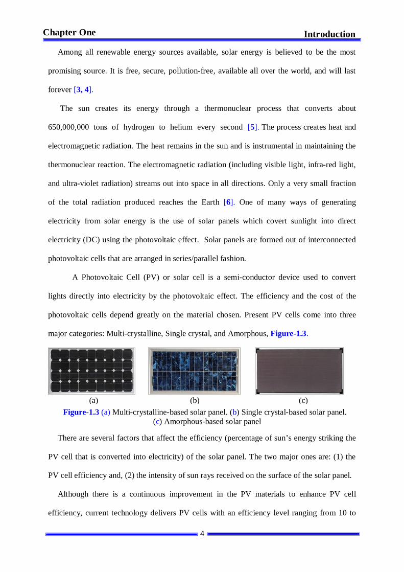
photovoltaic cells depend greatly on the material chosen. Present PV cells come into three
major categories: Multi-crystalline, Single crystal, and Amorphous, Figure-1.3.
There are several factors that affect the efficiency (percentage of sun’s energy striking the
PV cell that is converted into electricity) of the solar panel. The two major ones are: (1) the
PV cell efficiency and, (2) the intensity of sun rays received on the surface of the solar panel.
Although there is a continuous improvement in the PV materials to enhance PV cell
efficiency, current technology delivers PV cells with an efficiency level ranging from 10 to
Figure-1.3 (a) Multi-crystalline-based solar panel. (b) Single crystal-based solar panel. (c) Amorphous-based solar panel
(a) (b) (c)

5
Introduction Chapter One
20% (some laboratories reached efficiencies of more than 30% but not yet available
commercially). Therefore, to lower the per KWh cost, we need to rely on the dimensions of
the panels and/or the irradiation intensity. Increasing the surface area of the solar panels is not
a viable solution. It increases investments cost and requires more ground surface. A more
feasible and economical solution however, is to maximize power extraction from the panel by
operating the cell arrays at their full potential. This can be achieved by continuously exposing
the surface of the panel perpendicular to the sun’s rays. This strategy can be accomplished by
a sun tracker, a device onto which a solar panel is fitted to track the movement of the sun
across the sky (mimicking sunflower).
3 Sun Tracker Types
The efficiency of a photovoltaic panel depends on the incident angle of the sun rays with
respect to the surface of the panel. For the solar panel to harvest maximum energy from the
sun, a high-precision sun tracking system is necessary to track the sun in the sky from early
morning until late in the afternoon. A sun tracking system is a mechatronic system. It consists
of the mechanics, electric drives and information technology [7]. The mechanics consists
mainly of a tracker onto which a solar panel is fitted to track the movement of the sun by
maintaining the panel surface perpendicular to the sun incident radiations (mimicking
sunflower). The mechanics provide the necessary torque to change the azimuth and elevation
positions of the solar panel with respect to the sun, while the controller determines when and
how much to tune the driving motors to minimize the misalignment of the solar panel surface
with the sun’s incident rays.
Sun trackers are classified according to the number and orientation of their axes. They are
grouped into single- and dual-axis tracking devices. Single-axis trackers have one degree of
freedom. They are used to vary the azimuth angle in order to follow the movement of the sun
East-West during the day with fixed tilt angle. These types of trackers are more suitable in

6
Introduction Chapter One
tropical regions. Dual-axis trackers accommodate two degrees of freedom, azimuth and tilt.
Their axles are typically normal to one another. They have the capability to tune the solar
panel east-west and north-south and follow the sun’s apparent motion anywhere in the sky.
Figure 1.4 illustrates the structure of a dual-axis sun tracker. Angle is an azimuth angle of
the solar panel and is a tilt angle.
Motor 1 changes the azimuth angle along the east-west direction, whereas motor 2
changes the elevation angle along the north-south direction.
4 Sun Tracker Driving Modes
There are three methods of tracking: passive, chronological and active. Passive trackers
use a low boiling point compressed fluid (often Freon) as a means of tilting the solar panel.
When heated by the solar heat, it creates a gas pressure in the system, the fluid pressure
increases causing the liquid to move inside the tracker from one side to another allowing
gravity to rotate the tracker to follow the sun. These trackers do not use motors or control and
hence do not consume any energy. They are also less precise and therefore, operate with low
efficiency compared to active trackers. Passive trackers are however, unpractical in cold
locations. Chronological trackers employ electronic logic to control the actuators to follow the
sun based on mathematical formulae based on astronomical references with the data of a
whole one-year sun trajectory to calculate the sun movement in the sky. This data is usually
Figure 1.4 Structure of a dual-axis sun tracker
Azimuth angle
Tilt angle
E W
N
S
Motor 1
Motor 2
7
Introduction Chapter One
the current time, day, month and year of a specific geographical location. These trackers are
also known as open-loop trackers as they do not require any feedback for the controlled
system. Active trackers also known as closed-loop dynamic trackers on the other hand employ
motors and gear trains to direct the PV panel as commanded by the controller. They
commonly use light detecting sensors to provide raw data as inputs to the controller to track in
real-time the real position of the sun in the sky. They are more reliable than open loop
trackers. The use of the feedback makes their system response less sensitive to external
disturbances [8], [9].
5 Computing Platforms
At the heart of most embedded control systems is usually a real-time digital controlling
unit. Nowadays, designers are blessed by the variety of computing platforms they have at
their disposal to address these controlling units. These latter can be implemented using one or
a combination of design methodologies [10-11]. There are three major methodologies, namely:
(i) Dedicated (fixed) digital logic or application-specific integrated circuits or
ASICs,
(ii) Software-programmed logic platforms, and
(iii) Hardware reconfigurable logic platforms.
5.1 The ASIC Solution
There is no doubt, of all solutions; dedicated controllers or ASICs provide highest
performance as they are optimally tailored for particular use. They are great at speed and
power consumption. Moreover, they have reduced size and cost at high volume. They exhibit
high reliability of system operation. ASICs present some disadvantages. They are fixed
function integrated circuits, that is, the design is frozen in silicon with no possibility to make
any change.
8
Introduction Chapter One
5.2 Software-Programmed Logic
For years, digital designers largely relied on general-purpose microprocessors
microcontrollers, personal computers (PCs), digital signal processors (DSPs) and digital
signal controllers (DSCs) for the design of digital embedded systems. Despite the large
number of commercially available off-the-shelf products, designers of embedded systems are
often challenged to find the exact processor and the appropriate peripherals that will fit their
needs [12]. Often, designers must make compromises between performance, chip count,
flexibility, cost and power consumption in their choices.
Although flexible and able to implement complex algorithms, processor-based solution
presents some disadvantages. Off-the-shelf processors and peripheral devices have fixed
hardware, leaving software as the unique alternative to the designer to develop/enhance
his/her desired application. Moreover, the sequential nature of program execution with these
processors leads to several orders of magnitude inferior to ASICs in terms of performance,
silicon area usage and power consumption [10], [13].
5.3 Reconfigurable Logic or Programmable Hardware
In the above modalities, the hardware architecture is settled in the early stage of the design
cycle making even minor changes affect dramatically the ASIC design, processor selection
and printed-circuit board (PCB) design. An elegant and cost effective solution is obtained
when using the reconfigurability of the FPGA. In such computing platform, the system
hardware needs no longer to be frozen. The processor and peripheral devices as well as the
target FPGA can all be changed during development time, or migrated to new more
performant FPGA.
With today’s high density FPGAs, the emerging and revolutionary SoPC design
methodology provides a new paradigm in the design of embedded systems. This methodology
9
Introduction Chapter One
allows the integration of embedded processor(s) (hard-core and/or soft-core) with or without
user defined hardware accelerator blocks tailored to fit the desired application. The
heterogeneity of this approach allows the co-existence of the embedded microprocessor with
the FPGA logic in the same chip, taking the benefit of both the microprocessor and the ASIC.
Partitioning the controller into two main blocks makes the design process easier while
achieving better performance by avoiding the processor to get bogged down. The embedded
microprocessor will be used to implement non-timing critical functions, while timing critical
are best implemented as hardware accelerators in the FPGA fabric. To cope and design
efficient complex systems with this new paradigm, Altera for example provides sophisticated
and powerful electronic design automation (EDA) tools; Quartus II and the SoPC builder.
5.4 Implementation of Fuzzy Controllers
Fuzzy systems implementation has been exploited since the mid-1980s and different
architectures were devised. Naturally, the realization of these controllers will always be
digital because its algorithm is primarily based on rule inference using the “IF-THEN”
statements [14]. An efficient and effective implementation should satisfy two main
requirements: flexibility and performance. There exist two main branches of fuzzy systems
implementations: software and hardware implementations. A third branch can be a
combination of the first two.
Early fuzzy systems were mostly implemented in software by means of general-
purpose microprocessors, and microcontrollers. These implementations are flexible, require
the least hardware resources and can be developed rapidly. However, the sequential nature of
execution of these processors may not permit real-time processing.
Fuzzy systems hardware implementations can be realized as a dedicated hardware, as
an ASICs or on a reconfigurable FPGAs. Hardware implementations use a certain level of
parallelism and pipelining leading to a very high increase in processing speed. Nowadays,
10
Introduction Chapter One
with ceaseless increasing density of FPGAs and the SoPC approach, it is possible to takes
advantage of both the flexibility of software and the performance of hardware [15].
Several survey and review papers were published to highlight fuzzy systems
implementations. In [16], the authors reviewed many interesting fuzzy hardware/software
architectures from a categorical and historical point of view. Recently, in [17], Bosque et al
surveyed fuzzy systems and neural networks with a particular focus on hardware taxonomy
and highlighted the characteristics of the different applications covering the paradigms done
over the last two decades.
6 Structure of the Sun Tracking System
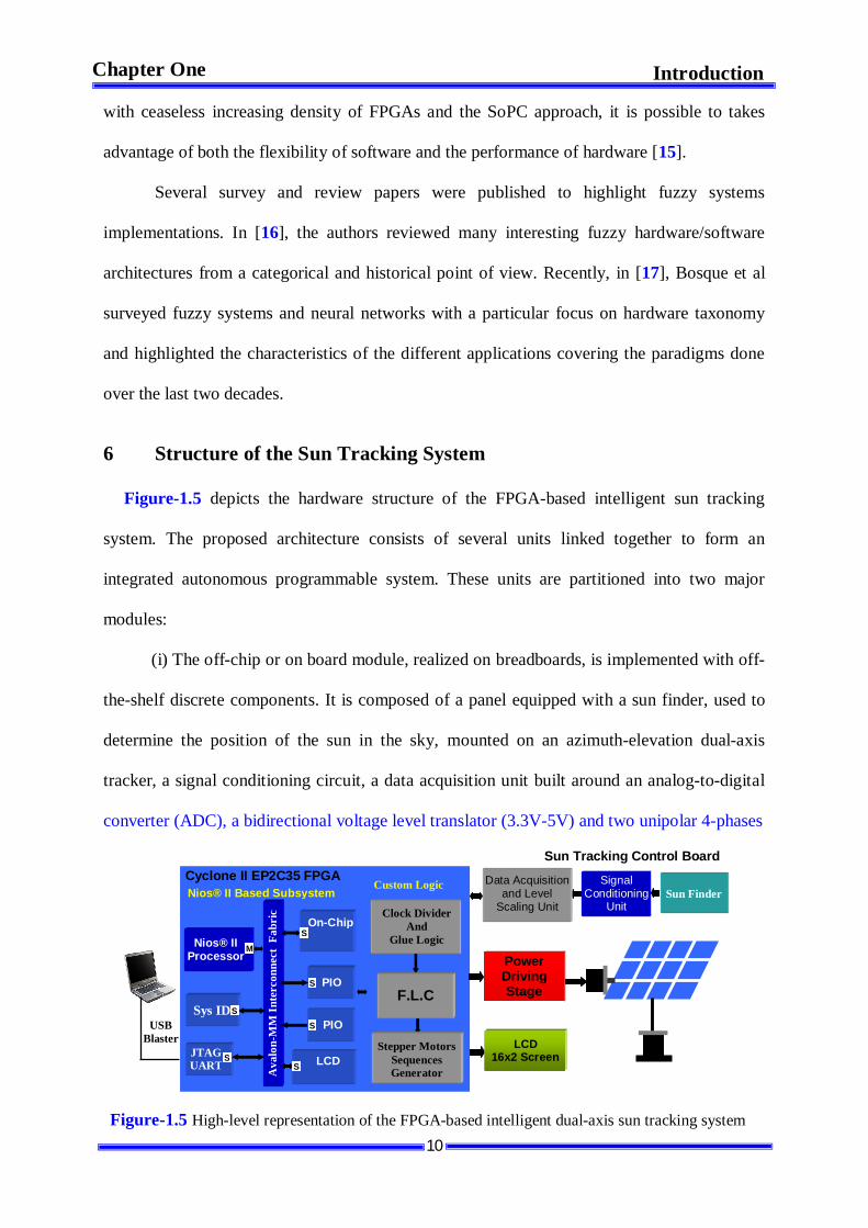
Figure-1.5 depicts the hardware structure of the FPGA-based intelligent sun tracking
system. The proposed architecture consists of several units linked together to form an
integrated autonomous programmable system. These units are partitioned into two major
modules:
(i) The off-chip or on board module, realized on breadboards, is implemented with off-
the-shelf discrete components. It is composed of a panel equipped with a sun finder, used to
determine the position of the sun in the sky, mounted on an azimuth-elevation dual-axis
tracker, a signal conditioning circuit, a data acquisition unit built around an analog-to-digital
converter (ADC), a bidirectional voltage level translator (3.3V-5V) and two unipolar 4-phases
USB Blaster
Cyclone II EP2C35 FPGA
Ava
lon-
MM
Int
erco
nnec
t Fa
bric
Nios® II Processor
JTAG UART LCD
On-Chip
Sys ID PIO
Nios® II Based Subsystem
PIO
M
S S
S
S
S S
Sun Tracking Control Board
Signal Conditioning
Unit
Sun Finder
Clock Divider And
Glue Logic
F.L.C
Stepper Motors Sequences Generator
Custom Logic Data Acquisition and Level
Scaling Unit
LCD 16x2 Screen
Power Driving Stage
Figure-1.5 High-level representation of the FPGA-based intelligent dual-axis sun tracking system
11
Introduction Chapter One
1.8° per step bidirectional stepper motors with their power driving circuits.
(ii) The on-chip module which is the digital controller is implemented onto the FPGA chip
of the low-cost DE2 board. The digital controller consists of two subsystems: a System-on-a-
Programmable-Chip or SoPC based subsystem built around the Altera Nios® II embedded
soft core processor and a custom non-SoPC subsystem. The SoPC Builder subsystem includes
several functional blocks such as the ADC interface, the liquid crystal display or LCD
controller, and an interface with the custom logic. It controls and gathers data from the data
acquisition unit by scheduling and generating the necessary signals to the analog-to-digital
converter, it performs the necessary data processing, monitoring and control of the external
actuators. The non-SoPC Builder subsystem consists of several custom hardware components
developed in VHDL that operates in conjunction with the processor-based system. The core
system of which is the fuzzy-like PD-type FLC and the stepper motors sequence generator.
7 Objectives of the Thesis
This thesis addresses the design process of a FPGA-based fuzzy logic controller (FLC)
applied to a sensors-driven dual-axis sun tracking system. The digital controller is
implemented using the SoPC approach. This methodology combines a soft processor core the
Nios® II, on-chip memory, intellectual property (IP) peripheral components and a user
defined hardware accelerator components integrated into a single FPGA device, Figure-1.6.
The approach combines the features of software programming and reconfigurable
hardware implementations into two inter-related modules: (i) a Nios® II embedded processor-
based subsystem which constitutes the upper layer of the digital controller and (ii) a PD-like
fuzzy logic module to steer the tracker actuators.
The first subsystem provides an ideal platform for microcontroller applications. Its
mission is to keep track of the data gathered from the sun finder unit by scheduling and
initiating the signals required by the data acquisition unit. It computes the angular errors and
12
Introduction Chapter One
the rates of change of these errors and applies them as crisp inputs to the PD-like fuzzy logic
module. In addition, the Nios® II subsystem controls the liquid crystal display (LCD) to
display in real-time the system’s status messages on a two-line LCD, and manipulates the
general-purpose input-output peripherals. The control program that runs on the Nios® II
processor is written in assembly language for highest performance and minimal code density.
The second module, the PD-like fuzzy logic module, which demands more computational
power, is designed and implemented in the FPGA’s massively parallel logic elements using a
handcrafted VHDL code as a custom reconfigurable application-specific accelerator
component to maximize parallel processing. The fuzzy logic module calculates the necessary
energy by which the system modifies the process in such a way the control objective can be
obtained.
The approach allows a processor to co-exist with custom logic in the FPGA fabric,
provides the flexibility to combine reconfigurable hardware and software based controls to
achieve a simple and better control of the sun tracker. This hardware/software solution runs
on an Altera low-cost Cyclone II FPGA, the EP2C35, to control the motion of two stepper
motors used as the mechanical drive system to keep the solar panel surface continuously
facing the sun during the day.
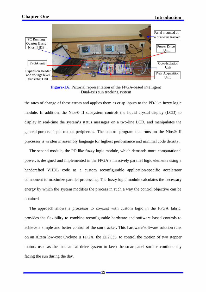
Figure-1.6. Pictorial representation of the FPGA-based intelligent Dual-axis sun tracking system
Expansion Header and voltage level
translator Unit
Power Drive Unit
Opto-Isolation Unit
Data Acquisition Unit
PC Running Quartus II and
Nios II IDE
FPGA unit
Panel mounted on a dual-axis tracker
13
Introduction Chapter One
8 Organization of the Thesis
This thesis is compiled into 7 chapters including this introduction and followed by
references used in this work. Chapter 1 introduced the problematic. It also reviewed existing
computing platforms used to implement digital controllers: processor-based and FPGA-based
with or without the SoPC technology.
In chapter 2, a literature review that surveys relevant research works on sun tracking
systems conducted in the last few decades is presented. Chapter 3 introduces fuzzy set theory
and fuzzy logic control. Chapter 4 presents background material to highlight the possibilities
and advantages using the FPGA. It also describes the most versatile and industry-standard
soft-core processor, the Nios® II as well as the emerging and revolutionary SoPC technology.
Chapters 5 and 6 constitute the bulk of the thesis. The former describes in details the
design and implementation of the fuzzy logic module. The latter begin by reviewing the
merits of the SoPC approach over the off-the-shelf processor and peripheral devices as
platforms for industrial applications. It lays out in detail the hardware and software design.
This chapter also presents the simulation and implementation of the FPGA-based intelligent
dual-axis sun tracking system. It reports the setup of the simulations and a prototyping real-
time implementation of the system which can be seen as a proof-of-concept. Chapter 7
concludes the thesis with some discussions and remarks for future research.
Finally, the thesis terminates with an extensive list of references for additional information
on the subject.
Part of the work reported in chapters 1, 5 and 6 has been published in [90].

14
Literature Review Chapter 2
Chapter 2
Literature Review
1 Introduction
Before diving into the practical of this thesis, a review of literature in the core area will be
presented with the aim to provide the reader with a survey on active sun tracking systems
using different types of computing platforms and control strategies, as well as developments
in FPGA-based designs with or without model-based fuzzy logic control systems. Also, we
report by whom, when and how.
Over the past four decades or so, a large number of contributions have been reported in
seminars and literature showing the increasing interest in the design and implementation of
sun tracking systems to increase their performances and efficiencies to harvest maximum
power from the solar panels mounted on trackers. Several control strategies as well as
different computing and control platforms have been used and tested to tackle this problem
[7], [8], [18-66]. These strategies can be categorized into three main classes: open-loop,
closed-loop and hybrid sun tracking control systems.
(i) Open-loop control strategies rely on a fixed control algorithm [7], [8], [18-29].
These controllers use mathematical formulae with the data of a whole one-year sun
trajectory to calculate the sun’s movement in the sky and need not sense the
sunlight to position the solar panel. This data is usually the current time, day,
month and year of a specific geographical location. The algorithms do not use any
15
Literature Review Chapter 2
feedback from the controlled system to determine if it has achieved or not the
desired goal.
(ii) Closed-loop types of sun tracking systems are based on feedback principles. They
usually use light sensors such as light dependent resistors (LDRs) to determine the
position of the sun in the sky with respect to the surface of the solar panel [8], [30-
37]. They are more reliable than open loop type controllers. The use of the
feedback makes their system response less sensitive to external disturbances.
(iii) Hybrid implementations, a strategy that combines both open- and closed-loop
control are also reported in literature [31], [38].
There is a large variety of techniques used to implement closed-loop type controllers.
These range from the On-Off control laws to more advanced techniques based on fuzzy logic
control including the classical controllers: the Bang-Bang controller, proportional-integral
(PI), proportional-derivative (PD) and proportional-integral-derivative (PID).
A myriad of physical implementations of sun tracking strategies are also reported in
literature. Similar to other industrial applications, these implementations have gone through
several stages of evolutions. They evolved from the early mechanical designs to the use of
discrete analog and digital standard integrated circuits. The general-purpose microprocessor-,
microcontroller- and DSP-based were the dominant platforms for the implementation and
realization of control algorithms based on conventional PID and alike, Bang-Bang and fuzzy
controllers. The use of the FPGA with or without the system-on-programmable-chip approach
emerged during the last decade.
2 Open-Loop Tracking Strategies
An open-loop type controller computes its input into a system using only the current state
and the algorithm of the system to determine if its input has achieved the desired goal. These
16
Literature Review Chapter 2
types of controllers based on mathematical algorithms/programs provide predefined
trajectories for the tracking system. These trajectories can be accurately determined because
the relative position of the sun can be precisely calculated at any time for any location on the
earth [7], [18] [19].
It is in 1975, that McFee [20] presented the first automatic solar tracking system. The
algorithm used to control the tracker computes the flux density distribution and the total
received power in a solar power system. Since that time, numerous works using open-loop
control have been carried out in the design and implementation of algorithms based on
astronomical formulae. They were used to drive electromechanical actuators to steer single-
and dual-axis sun tracking systems.
Semma et al [21] were among the first to use a microprocessor as a replacement of the
hard-wired logic used in earlier sun trackers to control the motion of a two-axis sun tracking
system. The controller was based on an active sun tracking approach and allows an array to
track the sun within five arc-minutes. This resulted in significant improvements in reliability
via parts screening and packaging and increased the functional capabilities of former basic
tracking systems.
In [22], the authors derived a general formula arguing that it embraces all the possible
one-axis tracking methods. To derive the formula, they used coordinate transformation
technique. This consists in transforming the sun’s position vector from earth-center frame to
earth-surface frame and then to collector-center frame. In doing so, they could resolve it into
solar azimuth and altitude angles relative to the solar collector making it simpler to the
controller to determine by how much it should tune the solar collector to minimize the
misalignment.
In 2004, Abdallah [23] designed and implemented four electromechanical open-loop solar
tracking systems: two-axis, one-axis vertical, one-axis east-west, and one-axis north-south in
17
Literature Review Chapter 2
order to investigate the effects of the current, voltage and power characteristics of a flat-plate
photovoltaic system compared to a fixed one with an inclination of 32° to the south. The
movement of the tracker was controlled by an algorithm in which the pre-calculated position
was programmed into a programmable logic controller (PLC). The author claimed that the
tracking systems increased the electrical powers of the collector by 43.87, 37.53, 34.43 and
15.69% respectively for the two-axis, one vertical axis, one-axis east-west and one-axis north-
south compared to that of the fixed one.
In paper [24], Grena describes an algorithm for obtaining highly precise values of the
solar position. Taking the fractional Universal Time (UT), the date, and the difference
between UT and Terrestrial Time (TT) (longitude, latitude, pressure and temperature) as
inputs, the algorithm computed the angular position of the earth with respect to the sun in the
ecliptic plane and then used this angle and the inclination angle of the earth’s rotational axis
to calculate the position of the sun.
In reference [25], the authors argued that the open-loop tracking strategies used to
compute the direction of the solar vector should be both accurate and computationally
straightforward to minimize the price of the tracking system. They developed an algorithm for
predicting the solar vector given knowledge of the time and the location.
In 2004, Reda et al [26] presented a simple step-by-step procedure for implementing a
solar position algorithm. In this algorithm, the solar zenith, azimuth and incident angles were
derived using ecliptic longitude and latitude for mean Equinox of data along with other
information. They reported that the solar zenith and azimuth angles could be calculated with
uncertainties of 0.0003°.
In [27] an open-loop control algorithm was developed to control a dual-axis sun tracking
system. The algorithm implemented into the LOGO-24 RC programmable logic controller
(PLC) is based on the mathematical definition of surface position. This latter is defined by
18
Literature Review Chapter 2
two angles: the slope of the surface and the surface azimuth angle. The authors used two
tracking motors, one for the joint rotating about the horizontal north-south axis to adjust the
slope of the surface and the other motor to rotate the collector about the vertical axis to
control the surface azimuth angle. A computer software has been developed to calculate the
optimal positions of the tracking surface during the daylight hours which were divided into
four identical time intervals. For each interval, the solar and motors speed are defined and
programmed into the PLC. The authors concluded the gain is considerable with an increase in
the daily collection of about 41.34° as compared to that of a fixed surface.
In 2010, Duarte et al [28] presented in an international conference on renewable energies
the design of a microcontroller-base two-axis solar tracker using solar maps. They employed
solar maps with the sun coordinates which depend on the time and geographical location.
Mousazadeh et al [29] and Lee et al [8] reviewed different types of sun-tracking systems.
They focused on the potential energy gain obtained by the application of both open- and
closed-loop algorithms. They surveyed some of the most significant proposals of both types
and discussed their pros and cons. They compared the outcomes of tracking systems with
fixed-position counterparts. They concluded that solar systems which track the changes in the
sun’s trajectory over the course of a day collect far greater amount of solar energy. They also
reported that the most efficient and popular sun-tracking devices was found to be in the form
of polar-axis and azimuth/elevation types.
3 Closed-Loop Tracking Strategies
Closed-loop types of sun tracking systems are based on feedback control principles
[8]. They use the concept of the open-loop for their forward path and feedback loop(s)
between the system’s output and input. In a closed-loop sun tracking system, light and image
sensors are in general used to discriminate the sun’s position and the induced signals
19
Literature Review Chapter 2
proportional to the sun light intensity employed as inputs to the controller. These data are
processed by the controller to automatically achieve and maintain the desired output
condition.
Roth et al [30] described the design and construction of an electromechanical automatic
sun-following system. They used a pyrheliometer to measure direct solar radiation. A four-
quadrant photo detector to sense the position of the sun and two small DC motors to move the
instrument platform are controlled by a Z80 microprocessor to keep the sun’s image at the
center of the four-quadrant photo detectors. The presented tracker can be adapted to work
with solar cell panels or concentrators. The interesting feature of this system is under cloudy
conditions, when the sun is not visible; a computing program calculates the position of the sun
and takes control of the movement, until the detector can sense the sun again. The same
authors described in [31] an improved version of their sun tracker. Although they kept the
same mechanical base they brought some novelties. The DC motors were replaced by stepper
motors, the four-quadrant sensor replaced by two sensors and the Z80 computing platform
was replaced by a microcontroller connected to a PC. The two sensors were used, one for sun
position information and the other to measure the sun light intensity. The tracker can operate
in two modes. In the clocked mode of operation, the position of the sun is calculated based on
the date and time information of its clock. Light position errors are measured during the day
and stored for later analysis. These data will be used the next day to compute more accurate
positions of the sun. In the active or sun mode of operation, the tracker uses the data of the
sun monitor to control the pointing.
In [32] Kalogirou described the design and construction of a one-axis sun tracking system
where the position and status of the sun are detected by three LDRs. One LDR is used to
detect the focus state of the collector; another one is responsible of detecting any cloud cover,
while the third is employed to discriminate daylight. The controller is constructed with
20
Literature Review Chapter 2
standard analog and digital integrated circuits. The actuator used in the tracker to point the
collector toward the sun is a low-power DC motor with speed-reduction gearbox. The author
reported that the deviation from the ideal posture is 0.2° and 0.05° with solar radiation of 100
and 600 Wm-2 respectively.
Recently, an image-based sun-tracking system was developed by Cheng. D. Lee et al [33].
The system consists of a self-design reflecting Cassegrain telescope, a webcam and an
embedded image processing algorithm to point to the sun. the central coordinates of the sun
images are calculated then sent to the solar tracker to follow the sun. Authors claimed that
their tracking system achieved a tracking accuracy of 0.04°.
In [34] Sefa et al designed and implemented a PC-based one-axis sun tracking system for
production of clean energy. The data from the two light sensors is collected by the
microcontroller-based data acquisition unit and transmitted serially to the PC for processing
and storage. Software developed in C language processes the collected data and instructs a
DC motor to follow the sun during day time. In addition, current, voltage and solar position
panel are displayed on the PC’s screen.
In reference [35], A. Konar et al employed a microprocessor to automatically position an
optimally tilted photovoltaic flat type solar panel for the collection of maximum solar
irradiation. The azimuth angle of the optimally tilted panel is controlled using one infrared
light detector. The technique used is similar to “perturb and observe” to determine maximum
irradiation. The use of step-tracking scheme instead of continuous tracking keeps the motor
idle for most of the time which results in power saving. The adjustment of the tilt angle is
done on a monthly basis. They suggested the use of a two-dimensional tracker for an
automatic tracking. We believe that the use of a second light detector would have not only
simplified the design but saved energy and motor aging due to continuous rotation in both
direction of the motor searching for optimal position of the solar collector.
21
Literature Review Chapter 2
Another microprocessor controlled automatic sun tracker is reported in [36]. Two light
sensors arranged in east-west direction are used to discriminate the position of the sun with
respect to the solar panel. A DC motor is gear coupled to rotate the panel along the east-west
direction to keep the panel perpendicular to the sun vector. Attached to the collector are two
switches used to limit the movement of the panel beyond its maximum angular positions in
the east and west directions.
In [37] Saxena et al designed and fabricated a microprocessor-based controller for a dual-
axis sun tracker to follow the sun in azimuth and altitude directions using two stepper motors.
The system operates in both open- and closed-loop modes. In closed loop mode the sensor
card provides signals to the controller. In open-loop mode, the tracker is brought to a pre-
calculated position depending on the month and time of the day.
In general, open-loop control systems are cheaper because they do not require any means to
gather feedback information such as light sensors. However, they present a major problem as
they have no error correction capabilities. In addition, a given algorithm is valid for a specific
location only. Closed-loop systems use sun finding position sensors. They are more reliable
than open-loop systems. However, they may not have capabilities to track the sun on cloudy
days. Hybrid control systems which consist of a combination of open- and closed-loop
strategies are also reported in literature [31], [38]. In such systems, the closed loop tracking
strategies are used to check and calibrate the astronomical control system.
4 FPGA-Based Tracking Strategies
A FPGA-based digital controller has many advantages compared to processor-based and
other platform types based controllers. It supports high-speed and concurrent control
algorithms, provides a higher degree of flexibility and a rapid low-cost manufacturing
solution. In the last decade, with high density FPGA chips, SoPC-based systems using Nios®
22
Literature Review Chapter 2
II soft core processor are being extensively used to implement control algorithms. This
reconfigurable computing approach is bringing a major revolution in the design of these
digital controllers. It allows the co-existence of the microprocessor with the user defined
hardware accelerators developed in HDL in a single chip instead of the mixed structure
microprocessor/FPGA [7], [39-48]. This approach is being adopted for its flexibility in
hardware and software, higher performance, reduced chip count and low cost.
In [39], Xinhong et al studied the applications of a FPGA development board to intelligent
solar tracking. Utilizing the Nios II Embedded processor, the authors developed a solar
tracking system. The two motors are controlled by a fuzzy logic module. The fuzzy controller
uses five fuzzy rules which reduce significantly the computation complexity in the real-time
control. The tracking systems can be operated into three modes: balance positioning, manual
mode and automatic mode. For the balance positioning, they used four mercury switches. In
the automatic mode, the fuzzy controller processes signals induced by four Cadmium sulphide
Photoresistors which discriminate the position of the sun in the sky. These signals are
digitized using four single-channel ADCs. The manual mode is used if the system has a fault
or needs to be maintained. The results of the experiment yielded more energy than the array as
a stationary unit. They reported that their system can achieve the maximum illumination and
energy concentration and cut the cost of electricity by requiring fewer solar panels, therefore,
it has significance for research and development.
In [40], the authors aimed to test whether FPGAs are able to achieve better position
tracking performance than software-based real-time platforms. The comparison was
conducted be embedding the same fuzzy logic controller (FLC) into a Virtex-II (XC2v1000)
FPGA from Xilinx and into software-based real-time platform NI CompactRIO-9002
architectures with the same sampling time. They concluded that the FPGA based FLC

23
Literature Review Chapter 2
exhibits much better performances (up to 16 times in the steady-state error, up to 27 times in
the overshoot and up to 19.5 times in the settling time) over the software-based FLC.
In publication [7], the authors dealt with an open-loop two-axis sun tracking for a PV
system. The tilt- and azimuth-angle trajectories of the tracking system are determined using
an optimization procedure based on a stochastic search algorithm called Differential
evolution. In this procedure, the objective function is evaluated by giving the models of
available solar radiation, tracking system consumption, and the efficiency of solar cells.
In [41], the authors describe the design of a stand-alone solar tracking system using a
FPGA. The design is based on astronomical equations to determine the position.
The basic software of the stand-alone tracking system is made up of (i) an Off-line
calculations of the sun path equations (developed in C), and (ii) a FPGA with suitable data to
the driving mechanical system.
Sun path equation determines the value of altitude and azimuth angles at any time of the
day. These values are stored as 8-bit words in a ROM. Two look-up tables were used, one for
the altitude angle and the other for the azimuth. The FPGA is designed to control the address
allocation for the look up tables stored in the ROMs for the sun tracking application. The
FPGA code is written in VHDL in Xilinx FPGA.
In [42], Monmasson et al reviewed the state of the art of FPGA design methodologies
with a focus on industrial control system applications. They review is followed with a short
survey on FPGA-based intelligent controllers for modern industrial systems. To illustrate the
benefits of an FPGA implementation using the proposed design methodology, two case
studies were presented. They consist of the direct torque control for induction motor
drives and the control of a diesel-driven synchronous generator using fuzzy logic.
In recent years, high density FPGA chips can efficiently integrate a reduced instruction set
computer (RISC) embedded soft-core processor, ready made intellectual property (IP)
24
Literature Review Chapter 2
peripherals and user defined hardware accelerator modules. A technology termed SoPC. This
hardware/software co-design combines the software-program executed by the embedded
processor to implement non-timing crucial repetitive control laws, while timing critical
intensive-computational functions are best implemented as hardware accelerator modules in
the FPGA logic. A large number of contributions using SoPC technology in different fields of
electrical engineering and control are reported in literature [49-54].
5 Fuzzy Control Tracking Strategies
Fuzzy control is the application of fuzzy logic to real-world control problems [55]. The first
fuzzy control application belongs to Mamdani & Assilian where the control of a small steam
engine is considered [56]. Since that time and due to its ease of use and robustness, fuzzy
control technology witnessed a wide range of applications in almost all areas. Applications of
fuzzy control include mechatronic systems (as manufacturing, robotics, automotive, etc),
nuclear industry, telecommunications, medical services etc. There are a lot of contributions
and reviews that illustrate the use of fuzzy control in industrial applications [55-66].
A fuzzy logic computer-controlled sun tracking system is described in [57]. This closed-
loop dual-axis tracking system is driven by two permanent magnet DC motors to provide
necessary torque to the PV panel. A PC-based basic fuzzy-like P-type controller with 14 fuzzy
rules was implemented. A data acquisition and a serial communication were implemented.
Back to 1999, in our opinion, it would have been simpler and more performant to use either
the parallel port or the Industry Standard Architecture (ISA) bus to interface the sun tracking
hardware circuitry with the PC.
In implementing a fuzzy system on a field programmable gate array, McKenna et al [58],
implemented a fuzzy control system in a FPGA to have a control surface as smooth as
possible. They used a weighted average approach to minimize the dimension of the look-up
table (LUT). The approach uses 3 or 4 most significant bits of each input to determine the
25
Literature Review Chapter 2
address for the LUT and to eliminate the rawness, the remaining bits are used to perform the
weighted average. Simulations were carried on using Matlab to verify the functionality of the
approach. The authors concluded that even with a large number of inputs, this approach helps
solve the exponential growth problem and complexity of LUT. The overall controller was
written in Verilog HDL and implemented in Xilinx 4000 series FPGA chip.
In [59], Kim presents the design and implementation of a fuzzy logic controller on a FPGA.
The controller is partitioned in many temporally independent functional modules, and each
implemented module forms a downloadable hardware object that can reconfigure the FPGA
chip. The controller was developed using the fuzzy logic controller Automatic
Implementation System (FADIS) tool. This latter performs various tasks in real-time such as
automatic VHDL code generation, synthesis, placement & routing and downloading. This
implementation method was effective in early 2000s when a single FPGA chip cannot fit the
controller due to the limited size of its capacity.
Poorani et al [60] advocate an approach to implement a fuzzy logic controller for motion
control using FPGA. This real-time implementation of the controller for four different types
of terrains is developed in VHDL and achieved on a Xilinx Spartan 2E board.
Precup and Hellendoorn [65] presented a survey on recent developments on analysis and
design of fuzzy control systems focused on industrial applications in the 2000. With a sample
of 244 references, the authors concluded that this can be viewed as a guarantee that future
successful applications will be constructed.
Also an interesting survey on analysis and design methods of model based fuzzy control
systems is given in [66].
This collection of papers is an interesting overview of the active research in the field of
programmed and reconfigurable hardware in embedded systems altogether with or without the
use of fuzzy logic control as a control strategy.

26
Chapter 3
Fuzzy Logic
1 Introduction
The Oxford English Dictionary defines the word “fuzzy” as “blurred, confused, vague,
imprecisely defined”. We should disregard this definition and view this word as a technical
adjective. As reminded by Lotfi. A. Zadeh, fuzzy logic is not fuzzy. Instead, fuzzy logic is a
precise logic for imprecision and approximate reasoning [67].
Fuzzy logic is viewed as a generalization of multi-valued logic compared to switching
(Boolean) logic which is a two-valued logic. It deals with degrees of membership and degrees
of truth. Unlike Boolean logic where variable can take at any instant of time a value that
belongs to the set {0, 1}, a fuzzy variable can take a value in the continuum [0, 1] of logic
values between 0 (completely false) and 1 (completely true).
In the literature, there are two kinds of justification for fuzzy systems theory: (i) the real-
world is too complicated for precise descriptions to be obtained; therefore, fuzziness should
be introduced to obtain reasonable, yet tractable models, (ii) human knowledge is increasingly
important as we move into the information era [68-70].
The objective of this chapter is to give an insight into this theory which allows the
formulation of the human knowledge in a systematic manner and puts it into engineering
systems when combined with other information such as sensory measurements [69].
Fuzzy Logic Chapter 3
27
2 Fuzzy Sets
Classical set theory deals with distinct and precise boundaries of inclusion. In this theory,
the membership of elements in a set is assessed in binary terms according to a bivalent
condition; en element either belongs to or does not belong to the set.
Let X denote the universe of discourse (or universal set), and x denotes the individual
elements in X. A classical (crisp) set A is defined by a characteristic function µA(x) that
assigns the values 1 or 0 to each element x, respectively, if x belongs or does not belong to A.
Formally, a classical set A in X is expressed as:
A = {(x, µA(x)) | x X; µA(x): X {0, 1}} (3.1)
Fuzzy set theory, however, deals with uncertainty and imprecision. In this theory, the
concept of characteristic function is extended into a more generalized form known as
membership function MF.
While the membership of elements in a crisp set is described by a bivalent condition, the
membership of elements in a fuzzy set is described by a multivalent condition. That is, the
MF can take any value between the unit interval [0, 1].
Formally, a fuzzy set A in X is expressed as:
A = {(x, µA(x)) | x X; µA(x): X [0, 1]} (3.2)
Note that curly brackets in equation 3.1 are used to refer to binary value, while square
brackets in equations 3.2 are used to represent a unit interval.
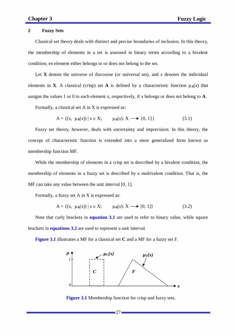
Figure 3.1 illustrates a MF for a classical set C and a MF for a fuzzy set F.
Figure 3.1 Membership function for crisp and fuzzy sets.
F C
µF(x) µC(x)
x
µ 1
0
Fuzzy Logic Chapter 3

28
2.1 Operations with Fuzzy Sets
This section deals with basic operations with fuzzy sets. In the classical set, its
membership function assigns a value of either 1 or 0 to each individual in the universe of
discourse, thereby discriminating between members and non-members of the crisp set under
consideration [68].
Consider A and B, two non-empty fuzzy sets in the universe of discourse X. For a given
element x X, the following function-theoretic operations are defined for A and B on X.
i. Complement
The complement of set A denoted by A , is defined as the collection of all elements in the
universe of discourse that do not reside in the set A.
In set theoretic form, it is expressed as
Aµ (x) = 1 - Aµ (x) for all x X (3.3)
ii. Union
The union or t-conorm of A and B is a fuzzy set in X, denoted by A B whose
membership function is defined as
A B = {x | x A V x B} for all x X.
For the t-conorm operator, we have
BAµ (x) = Aµ (x) V Bµ (x)
= max { Aµ (x), Bµ (x)} for all x X. (3.4)
iii. Intersection
The intersection or t-norm of A and B is a fuzzy set A B in X with membership function
defined as
A B = {x | x A x B} for all x X.
For the t-norm operator, we have
Fuzzy Logic Chapter 3
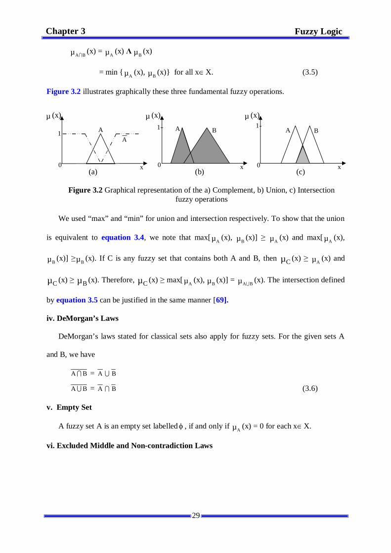
29
BAµ (x) = Aµ (x) Bµ (x)
= min { Aµ (x), Bµ (x)} for all x X. (3.5)
Figure 3.2 illustrates graphically these three fundamental fuzzy operations.
We used “max” and “min” for union and intersection respectively. To show that the union
is equivalent to equation 3.4, we note that max[ Aµ (x), Bµ (x)] Aµ (x) and max[ Aµ (x),
Bµ (x)] Bµ (x). If C is any fuzzy set that contains both A and B, then Cµ (x) Aµ (x) and
Cµ (x) Bµ (x). Therefore, Cµ (x) max[ Aµ (x), Bµ (x)] = BAµ (x). The intersection defined
by equation 3.5 can be justified in the same manner [69].
iv. DeMorgan’s Laws
DeMorgan’s laws stated for classical sets also apply for fuzzy sets. For the given sets A
and B, we have
BA = A B
BA = A B (3.6)
v. Empty Set
A fuzzy set A is an empty set labelled , if and only if Aµ (x) = 0 for each x X.
vi. Excluded Middle and Non-contradiction Laws
µ (x)
x 0
B A 1
µ (x)
x 0
B A 1
µ (x)
x 0
1 A A
Figure 3.2 Graphical representation of the a) Complement, b) Union, c) Intersection fuzzy operations
(c) (a) (b)
Fuzzy Logic Chapter 3
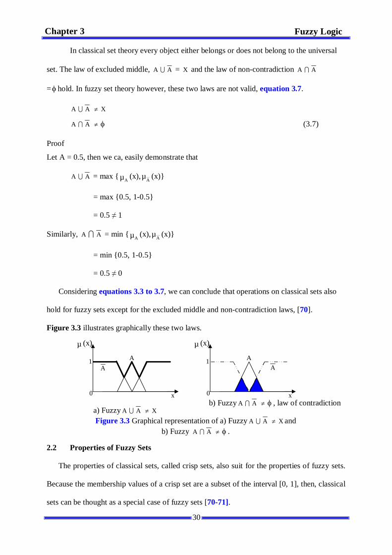
30
In classical set theory every object either belongs or does not belong to the universal
set. The law of excluded middle, A A = X and the law of non-contradiction A A
= hold. In fuzzy set theory however, these two laws are not valid, equation 3.7.
A A X
A A (3.7)
Proof
Let A = 0.5, then we ca, easily demonstrate that
A A = max { Aµ (x), Aµ (x)}
= max {0.5, 1-0.5}
= 0.5 1
Similarly, A A = min { Aµ (x), Aµ (x)}
= min {0.5, 1-0.5}
= 0.5 0
Considering equations 3.3 to 3.7, we can conclude that operations on classical sets also
hold for fuzzy sets except for the excluded middle and non-contradiction laws, [70].
Figure 3.3 illustrates graphically these two laws.
a) Fuzzy A A X 2.2 Properties of Fuzzy Sets
The properties of classical sets, called crisp sets, also suit for the properties of fuzzy sets.
Because the membership values of a crisp set are a subset of the interval [0, 1], then, classical
sets can be thought as a special case of fuzzy sets [70-71].
µ (x)
x 0
1 A A
b) Fuzzy A A , law of contradiction
µ (x)
x 0
1 A A
Figure 3.3 Graphical representation of a) Fuzzy A A X and b) Fuzzy A A .
Fuzzy Logic Chapter 3
31
We will use set notations rather than membership functions in order to make easy
comparison with classical sets.
Consider A, B, and C, three fuzzy sets in a non-empty universe of discourse X. the most
common properties of fuzzy sets include:
i. Commutativity
The commutativity property of two fuzzy sets using logical operators AND and OR is
given by
BA = AB
BA = AB (3.8)
ii. Associativity
The associativity property using logical operators AND and OR is given by
)CB(A = C)BA(
)CB(A = C)BA( (3.9)
iii. Distributivity
The distributivity property of three fuzzy sets using the AND and OR logical operators is
given by
)CB(A = )CA()BA(
)CB(A = )CA()BA( (3.10)
iv. Idempotency
The idempotency property of a fuzzy set A with respect to logical operators AND and OR
is given by
AA = A
AA = A (3.11)
v. Identity
Fuzzy Logic Chapter 3

32
The identity property of a fuzzy set A with respect to logical operators AND and OR and
given the empty set –having all degrees of membership equal to 0, and the universal set X
having all degrees of membership equal to 1 is defined as:
A = A and XA = A
A = and XA = X (3.12)
vi. Involution
The involution property which represents the double negation of a fuzzy set A is given by
A = A (3.13)
3 Membership Function
A fuzzy membership function (MF) is a graphical representation of a fuzzy set. It defines
how each point in the input space (universe of discourse) is mapped to a membership value
(or degree of membership) between 0 and 1.
The MF noted Aµ (x) describes the membership value of the element x of the universal set
X in the fuzzy set A. Figure-3.4 illustrates graphically fuzzy membership functions for speed.
It plots three fuzzy MFs one for each fuzzy set across the universe of discourse.
At crisp speed 85, the degree of membership (slow) is 0.0. The degree of membership
(normal) is 0.75 whereas for (fast) the degree of membership is 0.25.
Theoretically, membership functions can have any form of regular or irregular shapes as
long as they are convenient to be described mathematically [72]. Reasonably, designers adopt
Normal Fast Slow
80 100 60 85
1.0 0.75
0.25
0 speed
µ
Degree Of
Membership
Figure-3.4 Fuzzy membership functions for speed
Fuzzy Logic Chapter 3
33
regular shaped of known parameterized membership functions such as piece-wise linear
functions (triangular or trapezoidal) or nonlinear smooth functions such Gaussian, Sigmoidal
and Bell-shaped membership functions.
3.1 Piecewise Linear Membership Functions
Piecewise linear functions are the simplest from of MFs. Figure-3.5 illustrates a triangular
and a trapezoidal asymmetric membership functions.
3.1.1 Triangular Membership Function
A triangular MF is specified by three parameters: its peak (or center) m, left width a>0 and
right width b>0. It can be described through the equation:
It can also be expressed in a more compact form as:
µA(x) = max(min(m-bx-b ,
amax ), 0) (3. 15)
3.1.2 Trapezoidal Membership Function
A trapezoidal MF is specified by its tolerance (core) interval [a, b], the left width c and the
right width d. It is defined by the following equation
a b m X
µ 1
0
µ
b a c d X
1
0
0 x a
amax a x m
mbxb m x b
0 x b (3.14)
µA(x) =
cacx c x a
1 a x b
bdxd b x d
0 otherwise (3.16)
µA(x) =
Figure-3.5 Asymmetric triangular and trapezoidal membership functions (b) (a)
Fuzzy Logic Chapter 3

34
3.2 Features of the Membership Function
The feature of the membership function is defined by three properties. They are: core, support
and boundary. Figure-3.6 assists in the description of these three properties.
3.2.1 Core
The core of a membership function for a fuzzy set A is defined as the region of the universe of
discourse that is characterized by complete full membership in the set A, that is:
Core(A) = {x | Aµ (x) = 1} for all x X (3.17)
3.2.2 Support
The support of a membership function for a fuzzy set A is the set of points on the universe of
discourse where the membership grade in A is larger than 0, that is:
Supp(A) = {x | Aµ (x) > 1} for all x X (3.18)
3.2.3 Boundary
The boundaries of a membership function for some fuzzy set A are defined as that region of
the universe of discourse containing elements that have a nonzero membership but non
complete membership, that is:
Bnd(A) = {x | 0 < Aµ (x) < 1} for all x X (3.19)
3.2.4 Height
The height of a fuzzy set A is the peak value reached by the MF, also called supremum.
Formally, the height is defined as:
Core
Boundary
Support
Figure-3.6 Features of a membership function
Boundary
1
µ(x)
x
Fuzzy Logic Chapter 3
35
Hgt(A) = max { Aµ (x)} = )(sup xµAXx (3.20)
3.3 Structure of Membership Functions To illustrate the structure of MFs, figure-3.7 depicts a graphical representation of the
linguistic variable Temperature (T) with five partitions.
The universe of discourse is the range of all possible values applicable to a system
variable.
The label indicates the name used to identify a MF in each region of behaviour.
The scope or domain is the width of the MF. It is identified by a range of numerical
values that correspond to a label. Also, it indicates the range of concepts over which a
MF is mapped. These sub-divisions of the universe of discourse are usually uniform
but in certain cases some MFs can accumulate in zones where a more accurate control
(higher sensitivity) of the controller is desired and sparse elsewhere.
March [71] noted some interesting points which should be taken into account while defining
the domain of MFs:
- Every point in the universe of discourse should belong to the domain of at least
one MF.
- Two MFs cannot have the same point of maximal meaningfulness
- When two MFs overlap, the sum of membership grades for any point in the
overlap should be to 1.
Scope 10 20 30 40 0
Universe of Discourse
1
0
hot warm normal cool cold
T°
Figure 3.7 Graphical representation of a fuzzy variable with 5 fuzzy sets
Fuzzy Logic Chapter 3

36
- When two MFs overlap, the overlap should not cross the point of maximal
meaningfulness of either MF.
Another characteristic to be considered is the subdivision of the universe of discourse. This is
usually uniform, but in some applications the MFs can be denser in certain zones if higher
sensitivity of the controller is desired.
3.4 Number and Degree of Overlapping of Membership Functions
The number of MFs for each controller input as well as the shape and the overlapping
degree of the antecedents of the MFs has a strong influence on the characteristic of the fuzzy
logic controller.
The larger the number of MFs, the finer the fuzzy partitions of the controller inputs (higher
resolution) the better the approximation. However, more MFs means a larger number of
linguistic rules in the rule-base component and hence more computation complexity.
Moreover, this causes rapid firing of the fuzzy conclusions for changes in the inputs, resulting
in large output changes, which may cause instability in the system. On the contrary, few MFs,
result in a coarse fuzzy partitions of the input variables. With a reduced number of rules, the
controller does not require an intensive computation, it may however, cause a slower response
of the system and may even fail provide sufficient output control in time to recover for small
input changes. To date, there is no systematic approach to have an optimal fuzzy partition of
the fuzzy input/output, a rule of thumb is to have at least three and at most nine MFs for each
controller input [73].
The overlapping degree of the antecedents of MFs greatly influences the form of the
output of the fuzzy logic controller. Small overlapping degrees generate step characteristics,
whereas higher overlaps between MFs promote higher robustness of the controller and
generate smoother curves at the output.
3.5 Linguistic Variables and Linguistic Values
Fuzzy Logic Chapter 3

37
A sensor measures a variable and provides a numerical and precise value to the user.
Human perception however, evaluates a variable in linguistic terms i.e, in words. In order to
incorporate human perception into engineering systems in a systematic manner, input and
output variables of fuzzy logic based control systems are represented by variables that take
words as values [72]. Just as a variable that takes on a numerical value, for example 123.4, is
called an algebraic variable, a variable that can take words or sentences in natural or artificial
languages as its values is called a linguistic variable. These words or sentences, which form a
term set, are characterized by fuzzy sets defined in the universe of discourse in which the
variable is defined. A fuzzy partition, then, determines how many fuzzy sets should exist in
the term set, a number that determines the granularity of the linguistic variable. For example,
if cold, warm, hot, etc are values of temperature, then temperature is a linguistic variable and
these words are linguistic terms, values or labels.
In control systems, the linguistic variables are usually the error and the rate of change of
error where a term set is associated to each linguistic variable. The term set is usually
represented by the linguistic values or labels {NL, NM, NS, AZ, PS, PM, PL} where NL
means “Negative Large”, NM “Negative Medium”, NS “Negative Small”, AZ “Approximate
Zero”, PS “Positive Small”, etc.
The linguistic variables and the linguistic values provide a mean for the expert to express
his/her ideas about the decision-making process.
4 Fuzzy IF THEN Rules
Knowledge is the main source of intelligence [72]. In fuzzy control, knowledge is
expressed by a fuzzy rule-base model where each fuzzy linguistic rule is represented by a
fuzzy IF-THEN statement. The fuzzy conditional statement is symbolically expressed as:
IF < fuzzy proposition > THEN < fuzzy proposition >
where, a fuzzy proposition can have a value within the interval [0, 1].
Fuzzy Logic Chapter 3

38
The fuzzy proposition can be either an atomic or a compound proposition. An atomic
proposition is a single statement such as “IF Speed is Slow THEN… “ . Whereas a compound
proposition is made up of two or more atomic propositions connected by fuzzy union (OR) or
intersection (AND) operators such as “IF e is Large AND e is small THEN…”.
The IF-THEN linguistic rule consists of two parts: the “antecedent” (or premise) is the
block between the IF and THEN constructs whereas the “consequent” (or conclusion) is the
block following the THEN construct.
For example, the Mamdani-type fuzzy IF-THEN rule with multiple conjunctive
antecedents has the following form:
IF x1 is A1 AND x2 is A2 AND … AND xN is AN THEN y is B (3.21)
where xi, i = 1, 2, …, N and y are the input and output linguistic variables of the fuzzy system
respectively. The Ai’s and B are the linguistic values of the linguistic variables xi’s and y in
the universes of discourse Xi’s and Y respectively.
If standard mathematical notation for IF-THEN and AND is used, the above rule can be
reformulated as follows:
A1 (x1) A2 (x2) … AN (xN) => B (y) (3.22)
or µA1 (x1) µA2 (x2) … µAN (xN) => µB(y) (3.23)
where
µA1 (x1) µA2 (x2) … µAN (xN) = min { µA1 (x1), µA2 (x2), … , µAN (xN)} (3.24)
5 Properties of Fuzzy Rules
The fuzzy rule-base included into the knowledge base of a fuzzy control system consists
of a set of fuzzy rule list. For the fuzzy system to exhibit excellent performances the set of
fuzzy rules should cover all the possible situations that the system may face. Moreover, there
should not be any conflict among the fuzzy rules, while satisfying continuity. In other words,
Fuzzy Logic Chapter 3

39
the fuzzy rule list should fulfil the following three characteristics: completeness, consistency,
and continuity.
In order to define the above characteristics, it is desirable to consider a two-input one-
output fuzzy control system. The input linguistic variables x1 and x2 are partitioned into N and
M subspaces respectively, and represented by A1,A2, …, AN and B1, B2, …, BM on the
universe of discourse X. Table 3.1 shows the fuzzy rule list in the matrix form. The size of
the rule matrix depends on the number of system’s inputs and the number of fuzzy subspaces
representing these inputs. In general, the size of the matrix is the product of the fuzzy
subspaces of the system’s inputs.
5.1 Completeness
A set of fuzzy IF THEN rules {Ri, i = 1, 2,…, (NxM)} is complete, if for any x X it
produces an appropriate output value for any possible combination of input values.
Formally, completeness can be expressed as
(x1, x2): hgt( (x1, x2)) > 0
where denotes the output function of crisp inputs x1 and x2.
5.2 Consistency
A set of fuzzy IF THEN rules is consistent if it does not include any contradictory rule.
That is, two fuzzy rules with the same antecedent (IF part of rule) have mutually-exclusive
rule consequents (THEN part of rule), as for example
x2 y B1 B2 B2 B2 … BM
A1 R1,1 R1,2 R1,3 R1,4 … R1,M A2 R2,1 R2,2 R2,3 R2,4 … R2,M A3 R3,1 R3,2 R3,3 R3,4 … R3,M A4 R4,1 R4,2 R4,3 R4,4 … R4,M
…
……
x1
AN RN,1 RN,2 RN,3 RN,4 … RN,M
Table 3.1 The NxM set of fuzzy if-then rules in matrix form
Fuzzy Logic Chapter 3

40
Ri: IF RPQ THEN C
Rj: IF RPQ THEN C
5.3 Continuity
To define continuity we need the notion of fuzzy rule neighbourhood or adjacency. The
neighbor rules of rule Ri,j are R(i-1),j; Ri,(j-1); Ri,(j+1); R(i+1),j.
A set of fuzzy IF THEN rules satisfies continuity if there is no such a pair of neighboring
rules whose consequent fuzzy sets have empty intersection (are disjoint). The continuity of
fuzzy rules provides the continuity of controller output which is a desirable feature in control
applications.
When designing fuzzy logic control systems, completeness, consistency and continuity in
rule-base must be ensured otherwise, the system may encounter severe problems like
instability and/or oscillations behaviour [69], [73].
6 Fuzzy Logic Controller
Fuzzy control is based on fuzzy logic. It provides a formal methodology for representing,
manipulating and implementing a human’s heuristic knowledge, rather than traditional logical
systems, about how to control a system. The fuzzy logic controller which is an approximate
reasoning-based controller is a static nonlinear mapping between its inputs and outputs [72].
Similar to a conventional controller, from outside, both the input and output values of the FLC
are crisp values. The input values consist of measured values from the controlled plant or
some control errors computed from the measured values.
Figure 3.8 Shows the structure of a generic Mamdani-type fuzzy control system with n
inputs xi Xi where i = 1, 2, … , n and m outputs yi Yi where i = 1, 2, … , m where the
crisp sets Xi and Yi are universes of discourse for xi and yi respectively.
The fuzzy system is composed of four principle modules: a fuzzification interface, a fuzzy
knowledge-base, a fuzzy inference mechanism and a defuzzification interface. The processes
Fuzzy Logic Chapter 3
41
performed by these modules are executed sequentially. That is, before being processed by the
inference engine, the real-world (crisp) data inputs must first be fuzzified. Next, the
defuzzifier takes as inputs the fuzzy conclusions from the inference engine and provides a
result which will serve as an input to the object of control.
6.1 Fuzzification Interface
The first step in the fuzzy inference process is fuzzification. This mathematical encoding
procedure is performed by the fuzzification interface module. This module transforms the
crisp inputs applied to the fuzzy logic controller into fuzzy sets. Each crisp input will have its
proper set of MFs within the universe of discourse set, a set that holds all relevant values that
the crisp input can possess. The universe of discourse is partitioned into a number of fuzzy
sets where a MF is associated with each set. In general, the fuzzification interface module
performs the following functions:
i- Reads the real-world values of the input state variables,
ii- Performs a scale mapping that transfers the range of values of input variables into
the corresponding universe of discourse.
iii- Takes as inputs these scaled data and convert them into suitable linguistic format
by means of MFs used to quantify linguistic terms.
6.2 Fuzzy Knowledge-Base
FLC
x
Fuzzifier Interface
Fuzzy Inference
Engine
Fuzzified Inputs
y
Database
Rule Base
Defuzzifier Interface
Knowledge Base
Input MFs Fuzzy
Conclusions
Output MFs
Figure-3.8. Structure of a generic Mamdani type fuzzy logic controller.
m n
Fuzzy Logic Chapter 3

42
The fuzzy knowledge base encapsulates the human expert knowledge. This critical
module for the performance of the fuzzy logic controller has two sections: a database and a
rule base.
The database provides the necessary definitions for the fuzzification module, the rule base
component and the defuzzification interface module. It contains the MFs of the input and
output linguistic variables and the fuzzy sets used in the fuzzy rules. In addition, the database
includes fuzzy set definitions as well as other data (normalization/denormalization scaling
factors, processing periods, etc) which are required during the inference process.
The rule base of the controller is actually a list of fuzzy conditional IF-THEN statements
that quantify the actions a human expert would take to achieve a good control.
6.3 Fuzzy Inference Mechanism
The fuzzy inference engine is the kernel of the FLC. This crucial module emulates the
human expert’s decision-making about how to best achieve a desired control strategy of the
plant. It employs the linguistic rules provided by the rule-base component included in the
knowledge base module and the relevant fuzzified state variable inputs of the controlled
system to infer the fuzzy control actions for the controlled object. The combination of this
engine and the knowledge base constitutes the process of fuzzy reasoning system of a FLC.
The management of the fuzzy linguistic rules and the relevant fuzzified state variable
inputs to obtain the fuzzy control actions is one of the most important concerns in fuzzy
control systems. It is the inference mechanism. This latter consists of two sub-functions: (1)
fuzzy implication, and (2) aggregation of fuzzy conclusions.
6.3.1 Fuzzy Implication
Irrelevant of what the form and number of fuzzy rules we may have in the rule-base, the
main concern is how to interpret the meaning of each rule. That is, the process to determine
Fuzzy Logic Chapter 3

43
the influence produced by the antecedent part of the fuzzy rule on the conclusion part of the
rule. This procedure is known as the fuzzy implication.
There are many possible ways to define these implications. Two of the most commonly
used in control applications are: (1) the min(.), (known as Mamdani’s fuzzy implication)
which truncates the consequent’s membership function and, (2) the algebraic-product (known
as the Larsen’s fuzzy implication) which scales it.
In order to illustrate these two fuzzy implication types, we consider a fuzzy system with
two inputs x1 and x2 and a single output y is described by a set of linguistic IF-THEN rules in
the Mamdani’s form
Ri: IF x1 is i1A AND x2 is i
2A THEN y is iB for i= 1, 2,…, n (3.25)
where is i1A and i
2A are the fuzzy sets representing the i-th antecedent membership function
pairs and the iB is the fuzzy set representing the i-th conclusion.
For the i-th rule, the fuzzy implication function is given by
iRµ (x1, x2; y) = Ii ( iAµ
1(x1), iA
µ2(x2)) for i= 1, 2, …, n (3.26)
where Ii is an implication function.
i- The Mamdani’s implication is defined by the min(.) operator as:
iBµ (y) = min ( iAµ
1(x1), iA
µ2(x2)) for i= 1, 2, …, n (3.27)
ii- The Larsen’s implication is defined by the product operator as:
iBµ (y) = iAµ
1(x1) * iA
µ2(x2) for i= 1, 2, …, n (3.28)
6.3.2 Aggregation of Fuzzy Conclusions
Aggregation is the process of combining into a single fuzzy set the results of the fuzzy
rules obtained during the fuzzy implication phase. In fuzzy control, the individual rule-based
inference engine is usually used to compute the contribution of each activated (fired) rule. The
individual rules can be aggregated into a variety of ways. The most commonly used
Fuzzy Logic Chapter 3
44
aggregation operators are the maximum, the sum and the probalistic sum. Out of these three
operators, the best-known in literature and most frequently applied is the maximum. When
combined with the min(.) or product fuzzy implication operators, yields the well known Max-
Min also known as the Mamdani‘s inference method or the Max-Prod or the Larsen’s
inference method.
In the Max-Min inference, the membership functions of the fuzzy sets of the consequents
are limited to the degree of truth and in turn combined into a single fuzzy set by forming a
maximum, equation 3.29.
aggrBµ (y) = i
max [min [ iAµ
1(x1), iA
µ2(x2)]] for i= 1, 2, …, n (3.29)
In the Max-Prod however, the membership functions of the fuzzy sets of the consequents
are multiplied with the degree of truth of the condition and then combined, equation 3.30.
aggrBµ (y) = i
max [ iAµ
1(x1) * iA
µ2(x2)] for i= 1, 2,…, n (3.30)
Equations 3.27, 3.28, 3.29 and 3.30 are graphically represented in Figure-3.29. In this
figure each fuzzy rule antecedent and inference are shown in a separate line. The aggregation
Figure-3.9. Graphical representations of the Max-Min and Max-Prod inference methods of two rules of a two inputs system two with crisp inputs.
Rule 1
Rule 2
11A 1
2A
22A 2
1A
1B 1B
2B 2B
y
µ
µ
µ
µ
µ
µ
µ
µ
x1
x1
x2
x2 µ µ
y
y
y
y y
Antecedent MFs
Max-Min Max-Prod
Product
Product
Min
Min
Consequent MFs
Fuzzy Logic Chapter 3

45
of the consequents fuzzy sets are also shown vertically for both Max-Min and Max-Prod
operators. The symbols 11A and 1
2A refer to the first and second fuzzy antecedent of the first
fuzzy rule, while the symbol 1B refers to the fuzzy consequent of the first rule. Similarly, the
symbols 21A and 2
2A refer to the first and second antecedent of the second rule, and the symbol
2B refers to the fuzzy consequent of rule 2.
In the min(.) fuzzy implication, the inferred output of each rule is a fuzzy set chosen from
the minimum firing strength, whereas the Max-Min inference is the fuzzy union of the
resulting fuzzy conclusions, column 3. Graphically, the union of these two membership
functions is the outer envelop of the two shapes.
In the product fuzzy implication, the inferred output of each rule is a fuzzy set scaled
down by its firing strength via algebraic product, whereas the Max-Prod inference is also the
fuzzy union of the resulting fuzzy conclusions of the fuzzy implications, column 4.
6.4 Defuzzification Interface
Defuzzification is the final step in the fuzzy logic program. Although it is a part of the
fuzzy controller, the sole reason of this module is to provide an interface between the fuzzy
set domain and the real world crisp domain.
This mathematical decoding procedure is a mapping of fuzzy set actions, defined over an
output universe of discourse, implied by the fuzzy inference engine, into a space of non-fuzzy
actions. In this context, the resulting crisp value should provide the best representation of the
information inferred by the inference module.
Assume we have the result in Figure-3.10 at the end of the fuzzy inference procedure.
µ
y
- 1
Figure-3.10 Example of defuzzification for two-rule fuzzy inference
Fuzzy Logic Chapter 3

46
In this figure, the shaded area represents the fuzzy action result. The purpose of the
defuzzification module is to obtain a crisp value (represented by a dot in the figure) from the
fuzzy result.
There exist different defuzzification techniques proposed in the literature for defuzzifying
a fuzzy set described by a membership function. These techniques can be classified into two
principle groups based on their technical and structural characteristics [74]. They are: maxima
methods and distribution methods. Some of the most common defuzzifying techniques from
both classes will be described and graphically represented in the following sections.
6.4.1 Maxima Methods
The maxima methods have the common property that they select an element from the core
of a fuzzy set as defuzzification value. The strength of maxima methods is their simplicity and
speed of execution because they require passing through values of the core only.
The process consists in choosing the fuzzy set with the highest membership. The
remaining fuzzy sets are ignored and hence their information is lost. These defuzzifying
methods are not well suited in fuzzy logic controllers because they cannot guarantee the
continuity of the controller [72]. Maxima techniques can be classified as the first, the last or
the median maxima. These give rise to the following defuzzification techniques:
i- First of maxima (FOM)
ii- Last of maxima (LOM)
iii- Middle of maxima (MOM)
6.4.1.1 First Of Maxima (FOM)
The FOM, also called the left most maximum, method uses the union of the fuzzy sets and
takes the smallest value of the domain with the maximum membership degree, which is
expressed as:
Fuzzy Logic Chapter 3
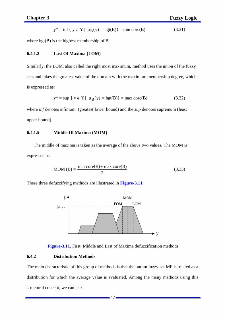
47
y* = inf { y Y | )y(µB = hgt(B)} = min core(B) (3.31)
where hgt(B) is the highest membership of B.
6.4.1.2 Last Of Maxima (LOM)
Similarly, the LOM, also called the right most maximum, method uses the union of the fuzzy
sets and takes the greatest value of the domain with the maximum membership degree, which
is expressed as:
y* = sup { y Y | )y(µB = hgt(B)} = max core(B) (3.32)
where inf denotes infimum (greatest lower bound) and the sup denotes supremum (least
upper bound).
6.4.1.5 Middle Of Maxima (MOM)
The middle of maxima is taken as the average of the above two values. The MOM is
expressed as
MOM (B) = 2
core(B)max core(B) min (3.33)
These three defuzzifying methods are illustrated in Figure-3.11.
6.4.2 Distribution Methods
The main characteristic of this group of methods is that the output fuzzy set MF is treated as a
distribution for which the average value is evaluated. Among the many methods using this
structural concept, we can list:
Figure-3.11. First, Middle and Last of Maxima defuzzification methods
y
µ FOM
MOM LOM µmax
Fuzzy Logic Chapter 3
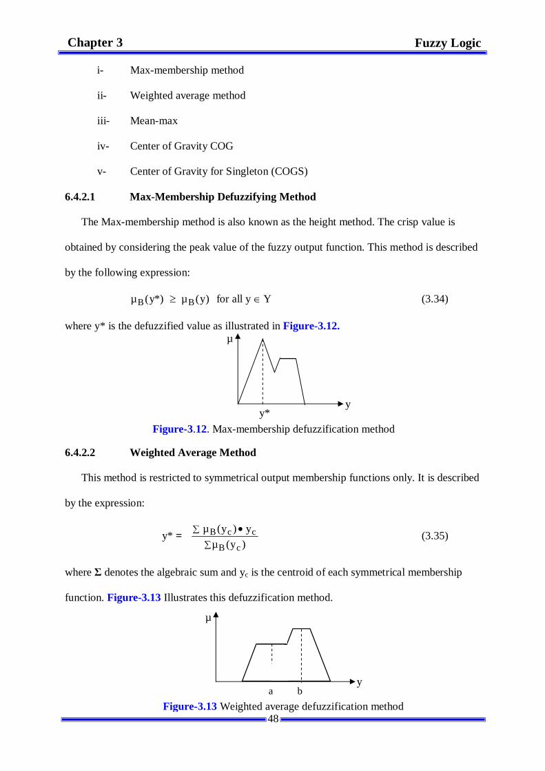
48
i- Max-membership method
ii- Weighted average method
iii- Mean-max
iv- Center of Gravity COG
v- Center of Gravity for Singleton (COGS)
6.4.2.1 Max-Membership Defuzzifying Method
The Max-membership method is also known as the height method. The crisp value is
obtained by considering the peak value of the fuzzy output function. This method is described
by the following expression:
*)y(µB )y(µB for all y Y (3.34) where y* is the defuzzified value as illustrated in Figure-3.12. 6.4.2.2 Weighted Average Method
This method is restricted to symmetrical output membership functions only. It is described
by the expression:
y* = )y(µy )y(µ
cB
ccB (3.35)
where denotes the algebraic sum and yc is the centroid of each symmetrical membership
function. Figure-3.13 Illustrates this defuzzification method.
Figure-3.12. Max-membership defuzzification method
y
µ
y*
Figure-3.13 Weighted average defuzzification method
y
µ
a b
Fuzzy Logic Chapter 3
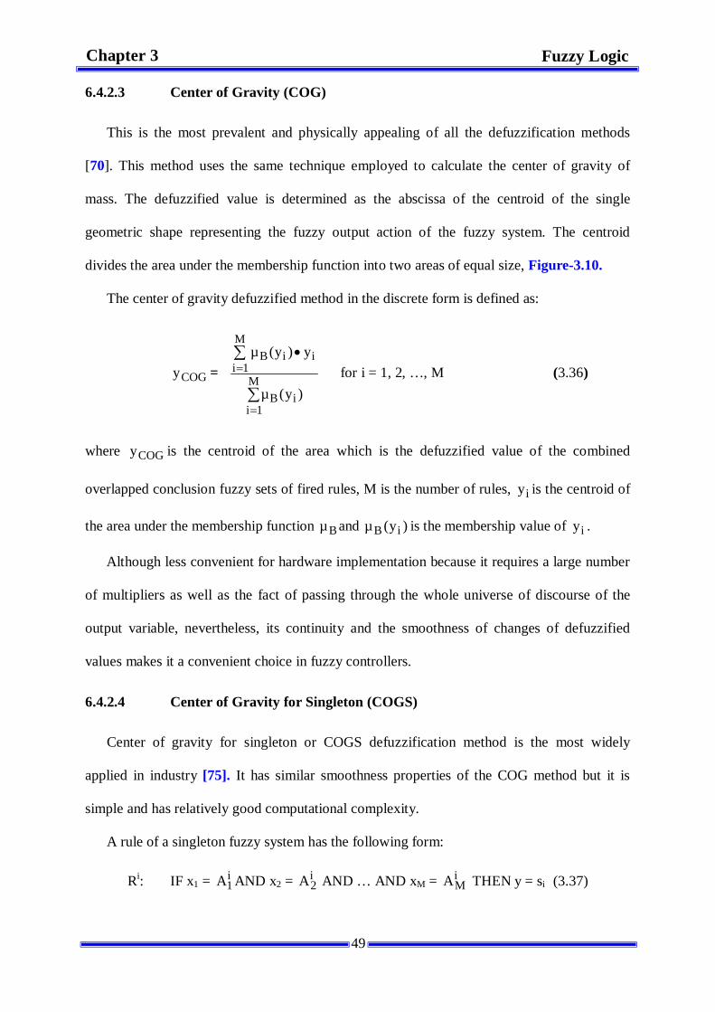
49
6.4.2.3 Center of Gravity (COG)
This is the most prevalent and physically appealing of all the defuzzification methods
[70]. This method uses the same technique employed to calculate the center of gravity of
mass. The defuzzified value is determined as the abscissa of the centroid of the single
geometric shape representing the fuzzy output action of the fuzzy system. The centroid
divides the area under the membership function into two areas of equal size, Figure-3.10.
The center of gravity defuzzified method in the discrete form is defined as:
COGy = M
1iiB
iM
1iiB
)y(µ
y)y(µ for i = 1, 2, …, M (3.36)
where COGy is the centroid of the area which is the defuzzified value of the combined
overlapped conclusion fuzzy sets of fired rules, M is the number of rules, iy is the centroid of
the area under the membership function Bµ and )y(µ iB is the membership value of iy .
Although less convenient for hardware implementation because it requires a large number
of multipliers as well as the fact of passing through the whole universe of discourse of the
output variable, nevertheless, its continuity and the smoothness of changes of defuzzified
values makes it a convenient choice in fuzzy controllers.
6.4.2.4 Center of Gravity for Singleton (COGS)
Center of gravity for singleton or COGS defuzzification method is the most widely
applied in industry [75]. It has similar smoothness properties of the COG method but it is
simple and has relatively good computational complexity.
A rule of a singleton fuzzy system has the following form:
Ri: IF x1 = i1A AND x2 = i
2A AND … AND xM = iMA THEN y = si (3.37)
Fuzzy Logic Chapter 3

50
where si is a real value called the singleton of rule i. It determines the position of the output
membership function of each rule which is a singleton.
The computation of the control signal value simplifies to a weighted sum since the output
MFs do not overlap.
The crisp output value is calculated using the expression of equation (3.38). Singletons is
are weighted by fuzzy output membership iµ for M such outputs, normalized to a degree of
truth of 1.
COGSy = M
1iii
iM
1iii
)s(µ
s)s(µ for i = 1, 2, …, M (3.38)
where COGSy denotes the result of defuzzification, M denotes the number of singletons, is is
the position of the output singleton i on the output variable universe of discourse and )s(µ ii
denotes the degree of truth of rule i according to the fuzzy implication.
Fuzzy Logic Chapter 3
51
FPGA Technology Chapter 4
Chapter 4
FPGA Technology
1 Introduction
FPGAs are at the leading edge of each new technology node. They are one of the largest
growing segments of the semiconductor industry. An FPGA is a semiconductor device. At the
highest level, it is a highly configurable silicon chip. This digital integrated circuit (IC) is
designed to be electrically configured by the customer after manufacturing to become almost
any customized digital system.
FPGAs belong to a large family of field programmable devices (FPDs). The three main
categories of FPDs are: simple programmable logic devices (SPLDs), complex PLDs
(CPLDs), and FPGAs. FPDs have grown from being used as simple “glue logic” to provide
programmable connectivity (such as address decoding, bus extender, etc) between major
components to today’s FPGAs where complete multi-processing system designs can be
implemented on a single chip.
The purpose of this chapter is to give an insight to the reader of the challenges to
implementing digital controllers with FPGAs. It describes a new paradigm which consists of
integrating the microprocessor and the FPGA architecture into a single device. In section two,
we relate a brief historical perspective of programmable logic. Section three deals with the
architecture of FPGAs. The last section is dedicated to the emerging technology the SoPC
along with one of the most versatile and industry-standard processor from Altera’s FPGA
design, the Nios® II soft core processor.
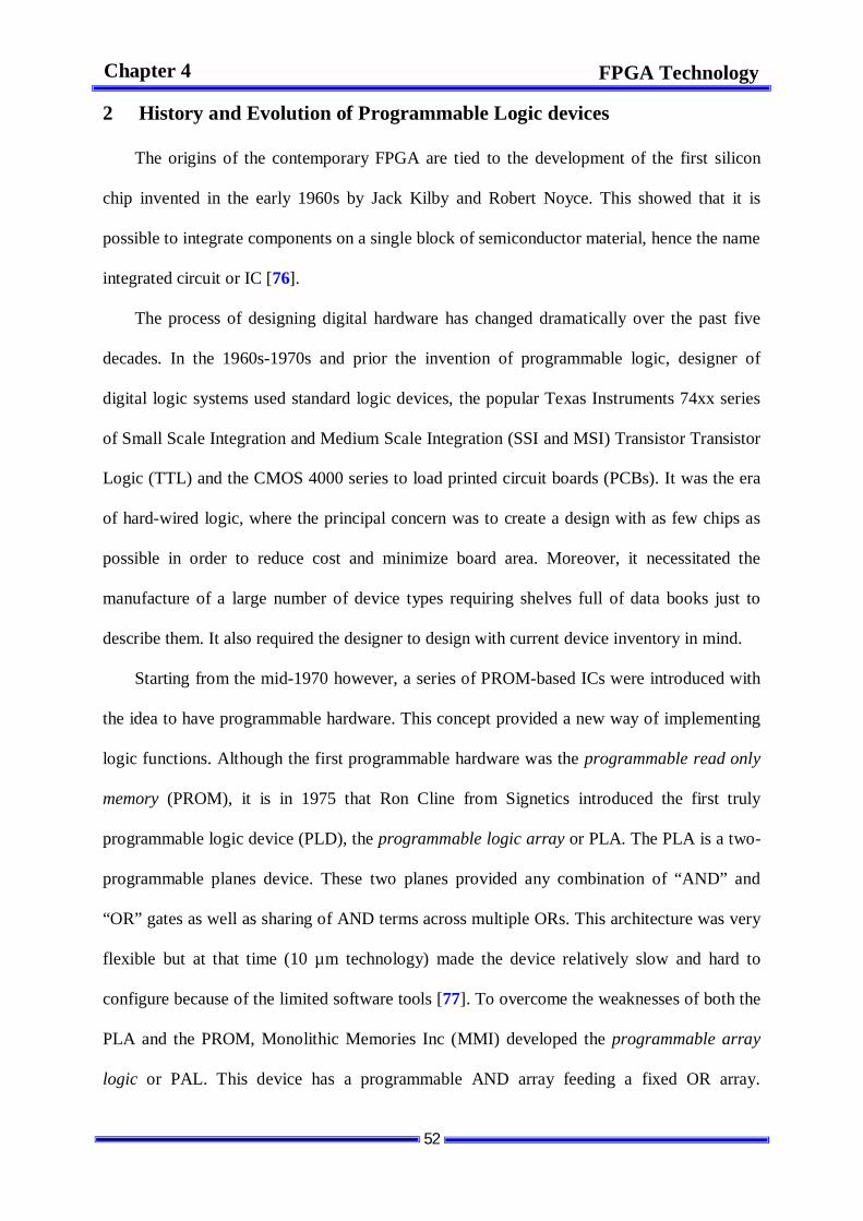
52
FPGA Technology Chapter 4
2 History and Evolution of Programmable Logic devices
The origins of the contemporary FPGA are tied to the development of the first silicon
chip invented in the early 1960s by Jack Kilby and Robert Noyce. This showed that it is
possible to integrate components on a single block of semiconductor material, hence the name
integrated circuit or IC [76].
The process of designing digital hardware has changed dramatically over the past five
decades. In the 1960s-1970s and prior the invention of programmable logic, designer of
digital logic systems used standard logic devices, the popular Texas Instruments 74xx series
of Small Scale Integration and Medium Scale Integration (SSI and MSI) Transistor Transistor
Logic (TTL) and the CMOS 4000 series to load printed circuit boards (PCBs). It was the era
of hard-wired logic, where the principal concern was to create a design with as few chips as
possible in order to reduce cost and minimize board area. Moreover, it necessitated the
manufacture of a large number of device types requiring shelves full of data books just to
describe them. It also required the designer to design with current device inventory in mind.
Starting from the mid-1970 however, a series of PROM-based ICs were introduced with
the idea to have programmable hardware. This concept provided a new way of implementing
logic functions. Although the first programmable hardware was the programmable read only
memory (PROM), it is in 1975 that Ron Cline from Signetics introduced the first truly
programmable logic device (PLD), the programmable logic array or PLA. The PLA is a two-
programmable planes device. These two planes provided any combination of “AND” and
“OR” gates as well as sharing of AND terms across multiple ORs. This architecture was very
flexible but at that time (10 µm technology) made the device relatively slow and hard to
configure because of the limited software tools [77]. To overcome the weaknesses of both the
PLA and the PROM, Monolithic Memories Inc (MMI) developed the programmable array
logic or PAL. This device has a programmable AND array feeding a fixed OR array.
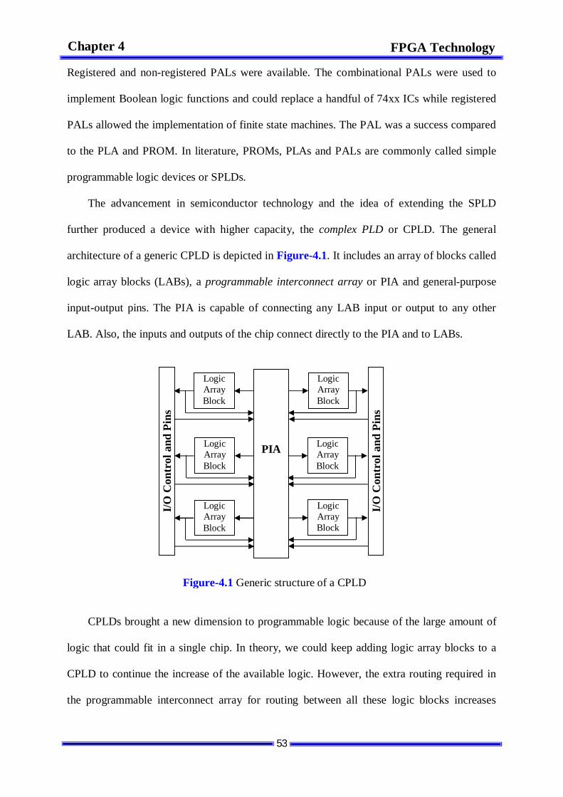
53
FPGA Technology Chapter 4
Registered and non-registered PALs were available. The combinational PALs were used to
implement Boolean logic functions and could replace a handful of 74xx ICs while registered
PALs allowed the implementation of finite state machines. The PAL was a success compared
to the PLA and PROM. In literature, PROMs, PLAs and PALs are commonly called simple
programmable logic devices or SPLDs.
The advancement in semiconductor technology and the idea of extending the SPLD
further produced a device with higher capacity, the complex PLD or CPLD. The general
architecture of a generic CPLD is depicted in Figure-4.1. It includes an array of blocks called
logic array blocks (LABs), a programmable interconnect array or PIA and general-purpose
input-output pins. The PIA is capable of connecting any LAB input or output to any other
LAB. Also, the inputs and outputs of the chip connect directly to the PIA and to LABs.
CPLDs brought a new dimension to programmable logic because of the large amount of
logic that could fit in a single chip. In theory, we could keep adding logic array blocks to a
CPLD to continue the increase of the available logic. However, the extra routing required in
the programmable interconnect array for routing between all these logic blocks increases
PIA
I/O C
ontr
ol a
nd P
ins
I/O C
ontr
ol a
nd P
ins
Figure-4.1 Generic structure of a CPLD
Logic Array Block
Logic Array Block
Logic Array Block
Logic Array Block
Logic Array Block
Logic Array Block
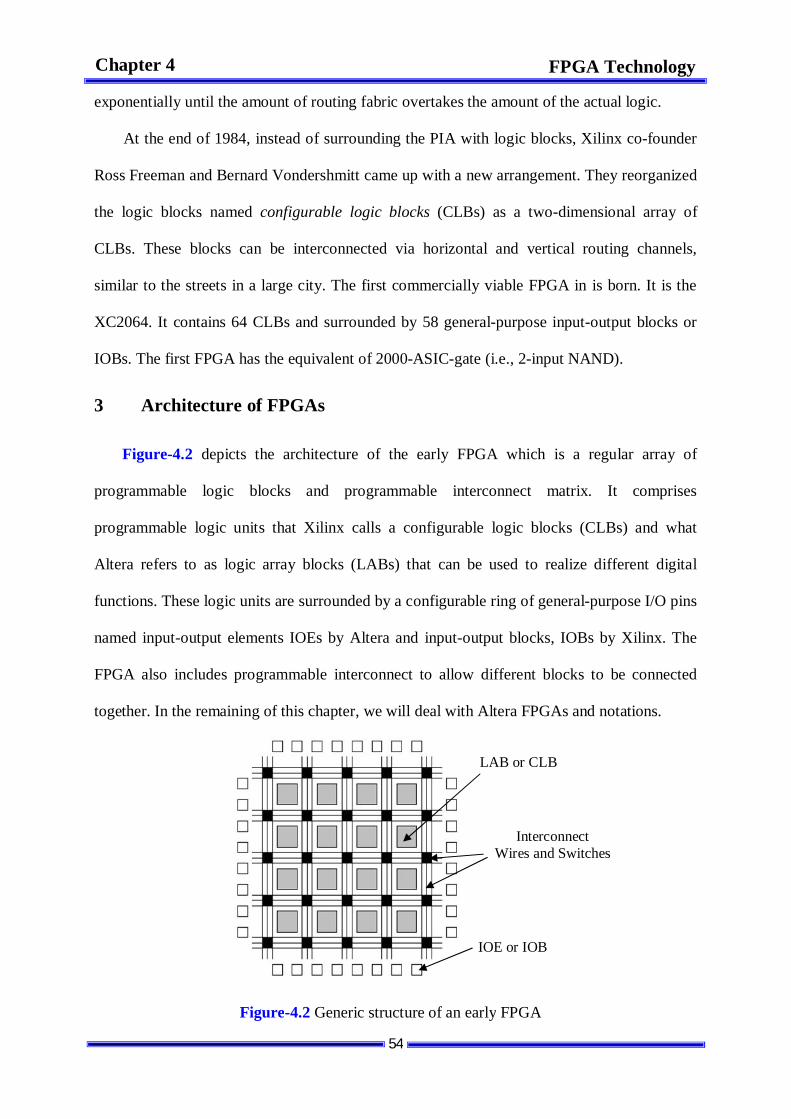
54
FPGA Technology Chapter 4
exponentially until the amount of routing fabric overtakes the amount of the actual logic.
At the end of 1984, instead of surrounding the PIA with logic blocks, Xilinx co-founder
Ross Freeman and Bernard Vondershmitt came up with a new arrangement. They reorganized
the logic blocks named configurable logic blocks (CLBs) as a two-dimensional array of
CLBs. These blocks can be interconnected via horizontal and vertical routing channels,
similar to the streets in a large city. The first commercially viable FPGA in is born. It is the
XC2064. It contains 64 CLBs and surrounded by 58 general-purpose input-output blocks or
IOBs. The first FPGA has the equivalent of 2000-ASIC-gate (i.e., 2-input NAND).
3 Architecture of FPGAs
Figure-4.2 depicts the architecture of the early FPGA which is a regular array of
programmable logic blocks and programmable interconnect matrix. It comprises
programmable logic units that Xilinx calls a configurable logic blocks (CLBs) and what
Altera refers to as logic array blocks (LABs) that can be used to realize different digital
functions. These logic units are surrounded by a configurable ring of general-purpose I/O pins
named input-output elements IOEs by Altera and input-output blocks, IOBs by Xilinx. The
FPGA also includes programmable interconnect to allow different blocks to be connected
together. In the remaining of this chapter, we will deal with Altera FPGAs and notations.
IOE or IOB
LAB or CLB
Interconnect Wires and Switches
Figure-4.2 Generic structure of an early FPGA
55
FPGA Technology Chapter 4
3.1 Logic Element
The core block in the Altera low cost cyclone device family of FPGAs is the logic element
(LE). LEs are compact and provide advanced features with efficient logic usage [78]. Figure-
3.3 illustrates a typical block diagram of a LE structure. The LE features a 4-input look-up
table (LUT), the carry chain connection and a programmable register (or flip flop). The LUT
is a function generator that can implement any function of four variables of a combinational
logic in an FPGA. It is internally implemented as a set of 2:1 multiplexers functioning as a
24:1 multiplexer. Multiplexer inputs are programmable, while select lines are the inputs of the
implemented functions. The sequential part of the LE comes from the programmable register,
which can be configured as a D, T, or JK flip-flop. The carry chain logic is required to link
the LE to other LEs. It also supports both register packing and feedback.
3.2 Logic Array Block
Moving one level higher in the hierarchy, we have the logic array block or LAB. The
LAB consists of 10 to 16 LEs, LAB control signals, LE carry chain, register chain and local
interconnect. Figure-3.4 depicts block diagram of a Cyclone II LAB.
The local interconnect transfers signals between LEs in the same LAB. Register chain
connections transfer the output of one LE’s register to the adjacent LE’s register within a
LAB [78]. The LAB local interconnect is driven by column and row interconnects and
4-input LUT
Carry Chain
Mux FF
Figure-4.3 Block diagram of the Altera logic element
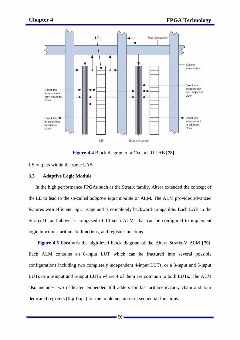
56
FPGA Technology Chapter 4
LE outputs within the same LAB.
3.3 Adaptive Logic Module
In the high performance FPGAs such as the Stratix family, Altera extended the concept of
the LE to lead to the so-called adaptive logic module or ALM. The ALM provides advanced
features with efficient logic usage and is completely backward-compatible. Each LAB in the
Stratix-III and above is composed of 10 such ALMs that can be configured to implement
logic functions, arithmetic functions, and register functions.
Figure-4.5 illustrates the high-level block diagram of the Altera Stratix-V ALM [79].
Each ALM contains an 8-input LUT which can be fractured into several possible
configurations including two completely independent 4-input LUTs, or a 3-input and 5-input
LUTs or a 6-input and 6-input LUTs where 4 of them are common to both LUTs. The ALM
also includes two dedicated embedded full adders for fast arithmetic/carry chain and four
dedicated registers (flip-flops) for the implementation of sequential functions.
Figure-4.4 Block diagram of a Cyclone II LAB [78]
LEs
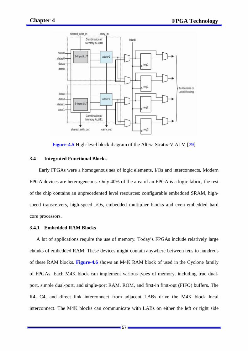
57
FPGA Technology Chapter 4
3.4 Integrated Functional Blocks
Early FPGAs were a homogenous sea of logic elements, I/Os and interconnects. Modern
FPGA devices are heterogeneous. Only 40% of the area of an FPGA is a logic fabric, the rest
of the chip contains an unprecedented level resources: configurable embedded SRAM, high-
speed transceivers, high-speed I/Os, embedded multiplier blocks and even embedded hard
core processors.
3.4.1 Embedded RAM Blocks
A lot of applications require the use of memory. Today’s FPGAs include relatively large
chunks of embedded RAM. These devices might contain anywhere between tens to hundreds
of these RAM blocks. Figure-4.6 shows an M4K RAM block of used in the Cyclone family
of FPGAs. Each M4K block can implement various types of memory, including true dual-
port, simple dual-port, and single-port RAM, ROM, and first-in first-out (FIFO) buffers. The
R4, C4, and direct link interconnect from adjacent LABs drive the M4K block local
interconnect. The M4K blocks can communicate with LABs on either the left or right side
Figure-4.5 High-level block diagram of the Altera Stratix-V ALM [79]
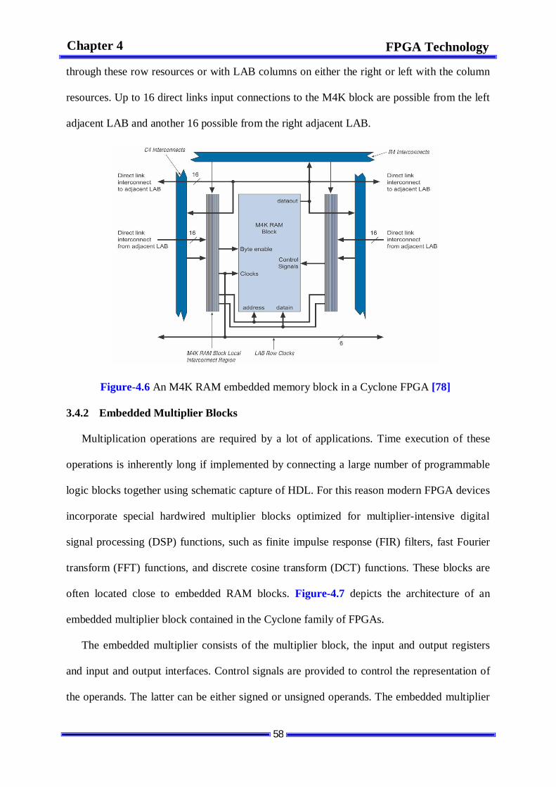
58
FPGA Technology Chapter 4
through these row resources or with LAB columns on either the right or left with the column
resources. Up to 16 direct links input connections to the M4K block are possible from the left
adjacent LAB and another 16 possible from the right adjacent LAB.
3.4.2 Embedded Multiplier Blocks
Multiplication operations are required by a lot of applications. Time execution of these
operations is inherently long if implemented by connecting a large number of programmable
logic blocks together using schematic capture of HDL. For this reason modern FPGA devices
incorporate special hardwired multiplier blocks optimized for multiplier-intensive digital
signal processing (DSP) functions, such as finite impulse response (FIR) filters, fast Fourier
transform (FFT) functions, and discrete cosine transform (DCT) functions. These blocks are
often located close to embedded RAM blocks. Figure-4.7 depicts the architecture of an
embedded multiplier block contained in the Cyclone family of FPGAs.
The embedded multiplier consists of the multiplier block, the input and output registers
and input and output interfaces. Control signals are provided to control the representation of
the operands. The latter can be either signed or unsigned operands. The embedded multiplier
Figure-4.6 An M4K RAM embedded memory block in a Cyclone FPGA [78]
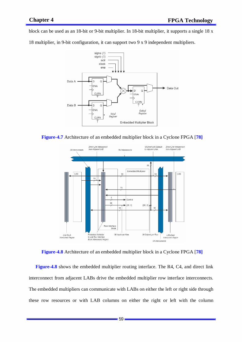
59
FPGA Technology Chapter 4
block can be used as an 18-bit or 9-bit multiplier. In 18-bit multiplier, it supports a single 18 x
18 multiplier, in 9-bit configuration, it can support two 9 x 9 independent multipliers.
Figure-4.8 shows the embedded multiplier routing interface. The R4, C4, and direct link
interconnect from adjacent LABs drive the embedded multiplier row interface interconnects.
The embedded multipliers can communicate with LABs on either the left or right side through
these row resources or with LAB columns on either the right or left with the column
Figure-4.7 Architecture of an embedded multiplier block in a Cyclone FPGA [78]
Figure-4.8 Architecture of an embedded multiplier block in a Cyclone FPGA [78]
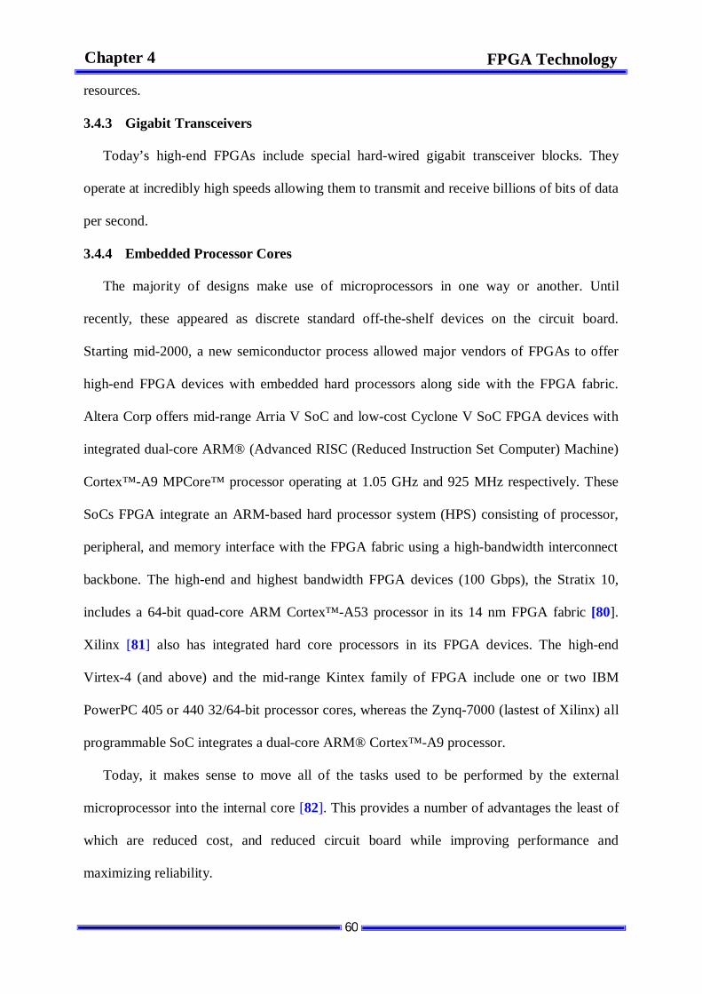
60
FPGA Technology Chapter 4
resources.
3.4.3 Gigabit Transceivers
Today’s high-end FPGAs include special hard-wired gigabit transceiver blocks. They
operate at incredibly high speeds allowing them to transmit and receive billions of bits of data
per second.
3.4.4 Embedded Processor Cores
The majority of designs make use of microprocessors in one way or another. Until
recently, these appeared as discrete standard off-the-shelf devices on the circuit board.
Starting mid-2000, a new semiconductor process allowed major vendors of FPGAs to offer
high-end FPGA devices with embedded hard processors along side with the FPGA fabric.
Altera Corp offers mid-range Arria V SoC and low-cost Cyclone V SoC FPGA devices with
integrated dual-core ARM® (Advanced RISC (Reduced Instruction Set Computer) Machine)
Cortex™-A9 MPCore™ processor operating at 1.05 GHz and 925 MHz respectively. These
SoCs FPGA integrate an ARM-based hard processor system (HPS) consisting of processor,
peripheral, and memory interface with the FPGA fabric using a high-bandwidth interconnect
backbone. The high-end and highest bandwidth FPGA devices (100 Gbps), the Stratix 10,
includes a 64-bit quad-core ARM Cortex™-A53 processor in its 14 nm FPGA fabric [80].
Xilinx [81] also has integrated hard core processors in its FPGA devices. The high-end
Virtex-4 (and above) and the mid-range Kintex family of FPGA include one or two IBM
PowerPC 405 or 440 32/64-bit processor cores, whereas the Zynq-7000 (lastest of Xilinx) all
programmable SoC integrates a dual-core ARM® Cortex™-A9 processor.
Today, it makes sense to move all of the tasks used to be performed by the external
microprocessor into the internal core [82]. This provides a number of advantages the least of
which are reduced cost, and reduced circuit board while improving performance and
maximizing reliability.

61
FPGA Technology Chapter 4
4 FPGA Programming Technologies
Three technologies are nowadays available for implementing reconfigurable FPGAs.
These are defined based on the way the routing between logic elements is configured. They
are: SRAM-, Flash- and Antifuse-based FPGAs.
4.1 SRAM-Based FPGA
The dominant type of FPGA devices is SRAM-based. This type is at the forefront of
FPGA technology, all large FPGAs are use this technology. Static memory cells are
distributed throughout the FPGA fabric to provide configurability. These memory cells (an
array of latches) is used to program interconnect and look up table (LUT) function levels.
Their major advantage is that new design ideas can be quickly implemented and tested. The
main downside is their volatility. Whenever the device is powered-off, the array of latches is
cleared losing the configuration of the design (bit-stream information) mapped into the FPGA
chip. Therefore, a back up battery is required when power is removed from the system, or the
programming information must be stored in a non-volatile media so that the FPGA can be
configured at power-on. In general, an electrically erasable programmable read only memory
(EEPROM) or flash memory device is used for this purpose.
4.2 Antifuse-Based FPGA
Antifuse programming technology is one-time programmable (OTP), that is, it cannot be
used for prototyping. Moreover, unlike SRAM-based FPGAs which are configured on site,
antifuse-based FPGAs are configured off-line using a special device programmer. Antifuse
are non volatile. This feature is of particular interest in some applications such as military and
aerospace because of high radiation tolerance. This type of FPGA is only fabricated by
Microsemi (previously Actel).
4.3 Flash-Based FPGA
Flash-based FPGAs use non-volatile memory cells to provide configurability. Their main
62
FPGA Technology Chapter 4
advantage is they do not require an external non-volatile memory to hold the configuration
information of the design. The major downside of this technology is the relatively smaller
density of integration, that is, flash cells are much larger than SRAM cells. They are also used
in military and aerospace because of high radiation tolerance.
5 Applications of FPGAs
Nowadays, FPGA devices are everywhere. They are widely used in both research and
industry. They provide market solutions and are key elements in a broad range of application
areas. In military applications FPGAs are found in radar and sonar as well as in secure
communications. Modern high definition video camera and displays integrate FPGA in their
circuitry. FPGA devices are widely used in industry. We can find them in motor/motion
control, smart energy, machine vision, medical imaging and industrial Ethernet.
Another area of application of FPGA devices is application-specific integrated circuit
(ASIC) and application specific standard product (ASSP) prototyping. Because the FPGA
platforms provide a faster, smoother path to delivering an end working product, they are used
in the verification of both register transfer level (RTL) and initial software development of
ASIC and ASSP devices. This standard practice not only provides the opportunity to have a
hardware platform early in the design cycle, it also decreases development time and reduces
the risk of silicon failure.
6 The Nios® II and SoPC Builder
6.1 The Nios® II Processor
The Netware Input-Output Subsystem, Nios® II, is the Altera’s flagship intellectual
property (IP) second generation soft-core processor. It is a 32-bit embedded processor
designed and optimized for the use in FPGA designs targeting Altera’s mainstream FPGA
families [83-84].
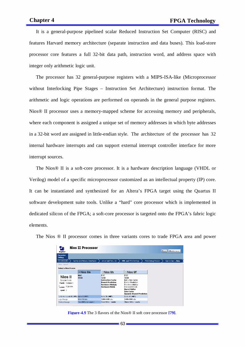
63
FPGA Technology Chapter 4
It is a general-purpose pipelined scalar Reduced Instruction Set Computer (RISC) and
features Harvard memory architecture (separate instruction and data buses). This load-store
processor core features a full 32-bit data path, instruction word, and address space with
integer only arithmetic logic unit.
The processor has 32 general-purpose registers with a MIPS-ISA-like (Microprocessor
without Interlocking Pipe Stages – Instruction Set Architecture) instruction format. The
arithmetic and logic operations are performed on operands in the general purpose registers.
Nios® II processor uses a memory-mapped scheme for accessing memory and peripherals,
where each component is assigned a unique set of memory addresses in which byte addresses
in a 32-bit word are assigned in little-endian style. The architecture of the processor has 32
internal hardware interrupts and can support external interrupt controller interface for more
interrupt sources.
The Nios® II is a soft-core processor. It is a hardware description language (VHDL or
Verilog) model of a specific microprocessor customized as an intellectual property (IP) core.
It can be instantiated and synthesized for an Altera’s FPGA target using the Quartus II
software development suite tools. Unlike a “hard" core processor which is implemented in
dedicated silicon of the FPGA; a soft-core processor is targeted onto the FPGA’s fabric logic
elements.
The Nios ® II processor comes in three variants cores to trade FPGA area and power
Figure-4.9 The 3 flavors of the Nios® II soft core processor [79].
64
FPGA Technology Chapter 4
consumption for speed of execution. These flavors are: fast, standard and economy, Figure-
4.9. Each core version modifies the number of pipeline stages, cache memories for data and
instructions, number of cycles per instruction, addressable memory space, and hardware or
software implementation of multiplication and division operations and so on.
i- The fast version (Nios® II/f) is designed for performance-critical applications at
the expense of core size. It includes separate optional instruction and data caches,
where caches are implemented in the FPGA memory blocks. It employs a 6-stage
pipeline to achieve maximum DMIPS/MHz. This high performance variant
provides optional hardware multiply, divide, and shift options to improve
arithmetic performance. It executes one instruction per cycle. When the memory
management unit (MMU) is present, the processor can access up to 4 GBytes of
memory.
To give the processor a fast access to the on-chip memory, the Nios® II fast
core architecture provides optional tightly-coupled memory interface arrangements
(memory connected directly to the processor) for both instructions and data. When
the tightly-coupled memory is present, its access bypasses cache memory.
ii- The standard core version (Nios® II/s) is optimized for medium-performance and
cost-sensitive applications. It employs a 5-stage pipeline. Unlike the fast version,
the standard has an instruction cache, but no data cache.
iii- The economy variant (Nios® II/e) is designed with the smallest possible logic
utilization of FPGA. It is not pipelined (one stage) and contains no cache. It has a
limited feature set, and many settings are not available when this version is
selected, Figure-4.9. The economy variant executes at most one instruction per six
clock cycles. The major advantage of this core is it is licence free while the /f and
/s versions require a $500/year licence.
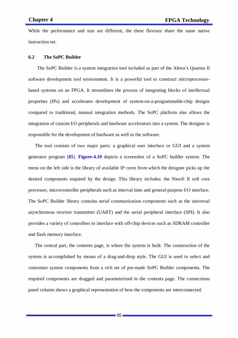
65
FPGA Technology Chapter 4
While the performance and size are different, the three flavours share the same native
instruction set.
6.2 The SoPC Builder
The SoPC Builder is a system integration tool included as part of the Altera’s Quartus II
software development tool environment. It is a powerful tool to construct microprocessor-
based systems on an FPGA. It streamlines the process of integrating blocks of intellectual
properties (IPs) and accelerates development of system-on-a-programmable-chip designs
compared to traditional, manual integration methods. The SoPC platform also allows the
integration of custom I/O peripherals and hardware accelerators into a system. The designer is
responsible for the development of hardware as well as the software.
The tool consists of two major parts: a graphical user interface or GUI and a system
generator program [85]. Figure-4.10 depicts a screenshot of a SoPC builder system. The
menu on the left side is the library of available IP cores from which the designer picks up the
desired components required by the design. This library includes: the Nios® II soft core
processor, microcontroller peripherals such as interval time and general-purpose I/O interface.
The SoPC Builder library contains serial communication components such as the universal
asynchronous receiver transmitter (UART) and the serial peripheral interface (SPI). It also
provides a variety of controllers to interface with off-chip devices such as SDRAM controller
and flash memory interface.
The central part, the contents page, is where the system is built. The construction of the
system is accomplished by means of a drag-and-drop style. The GUI is used to select and
customize system components from a rich set of pre-made SoPC Builder components. The
required components are dragged and parameterized in the contents page. The connections
panel column shows a graphical representation of how the components are interconnected.
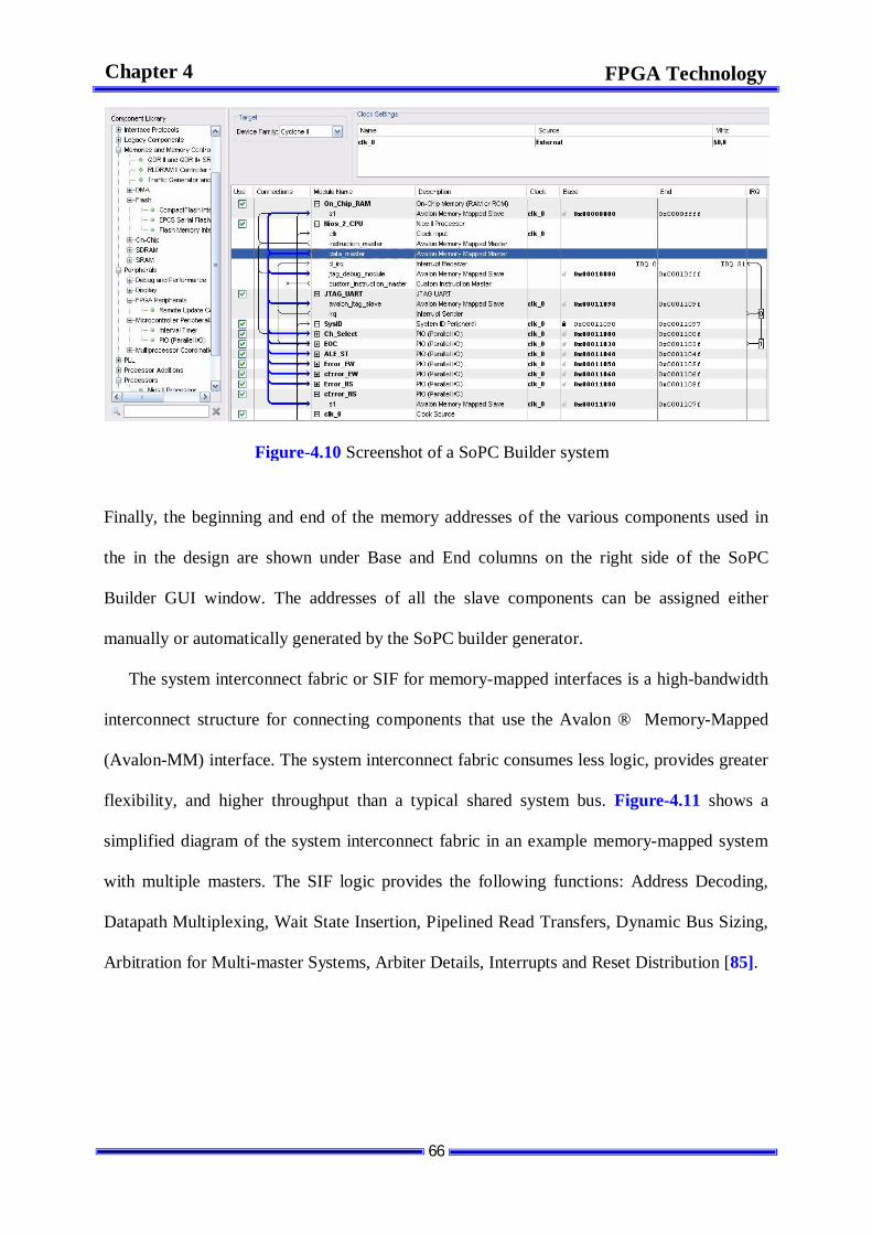
66
FPGA Technology Chapter 4
Finally, the beginning and end of the memory addresses of the various components used in
the in the design are shown under Base and End columns on the right side of the SoPC
Builder GUI window. The addresses of all the slave components can be assigned either
manually or automatically generated by the SoPC builder generator.
The system interconnect fabric or SIF for memory-mapped interfaces is a high-bandwidth
interconnect structure for connecting components that use the Avalon ® Memory-Mapped
(Avalon-MM) interface. The system interconnect fabric consumes less logic, provides greater
flexibility, and higher throughput than a typical shared system bus. Figure-4.11 shows a
simplified diagram of the system interconnect fabric in an example memory-mapped system
with multiple masters. The SIF logic provides the following functions: Address Decoding,
Datapath Multiplexing, Wait State Insertion, Pipelined Read Transfers, Dynamic Bus Sizing,
Arbitration for Multi-master Systems, Arbiter Details, Interrupts and Reset Distribution [85].
Figure-4.10 Screenshot of a SoPC Builder system
67
FPGA Technology Chapter 4
Figure-4.11 System interconnect fabric with multiple mastering components [85]

68
Design of the Fuzzy Logic Module
Chapter 5
Chapter 5
Design of the Fuzzy Logic Module
1 Introduction
Sun is permanently changing its position in the sky. Everyday, it moves from east to west
between sunrise and sunset; the azimuth movement. It also, moves from north to south
throughout the course of the year; the elevation movement. Because the energy extracted from
the PV panel is at its maximum when the surface of the solar panel is perpendicular to the
sun’s rays, then an ideal tracking system should maintain a solar panel accurately pointing
towards the sun, compensating for both changes in the azimuth and elevation angles of the
sun with respect to the panel throughout the day. It is desirable to develop a control system
based on fuzzy logic methodology to fulfill these requirements.
Fuzzy control is based on fuzzy logic which is close in spirit to human thinking and
natural language [86]. It provides a convenient way to build the control strategy by requiring
only qualitative knowledge for the behavior of the control system. In recent years, fuzzy
control is used to enhance control engineering solutions. It brought high promising
alternatives to conventional controllers by providing higher degree of robustness (immunity to
external disturbance) and by achieving better performances (short rise-time, small overshoot)
over linear controllers [87]. Fuzzy controllers revolutionized the field of control engineering
by their ability to perform process control by the utilization of human knowledge, thus
enabling solutions to control problems for which mathematical models may not exist, or may
be too difficult or computationally too expensive to construct [88].
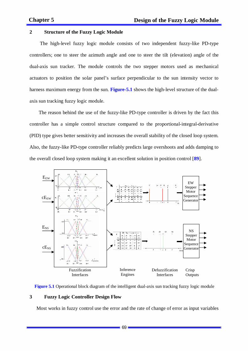
69
Design of the Fuzzy Logic Module
Chapter 5
2 Structure of the Fuzzy Logic Module
The high-level fuzzy logic module consists of two independent fuzzy-like PD-type
controllers; one to steer the azimuth angle and one to steer the tilt (elevation) angle of the
dual-axis sun tracker. The module controls the two stepper motors used as mechanical
actuators to position the solar panel’s surface perpendicular to the sun intensity vector to
harness maximum energy from the sun. Figure-5.1 shows the high-level structure of the dual-
axis sun tracking fuzzy logic module.
The reason behind the use of the fuzzy-like PD-type controller is driven by the fact this
controller has a simple control structure compared to the proportional-integral-derivative
(PID) type gives better sensitivity and increases the overall stability of the closed loop system.
Also, the fuzzy-like PD-type controller reliably predicts large overshoots and adds damping to
the overall closed loop system making it an excellent solution in position control [89].
3 Fuzzy Logic Controller Design Flow
Most works in fuzzy control use the error and the rate of change of error as input variables
Figure 5.1 Operational block diagram of the intelligent dual-axis sun tracking fuzzy logic module
EW Stepper Motor
Sequence Generator
NS
Stepper Motor
Sequence Generator
EEW
cEEW
cENS
ENS
Fuzzification Interfaces
Inference Engines
Defuzzification Interfaces
Crisp Outputs
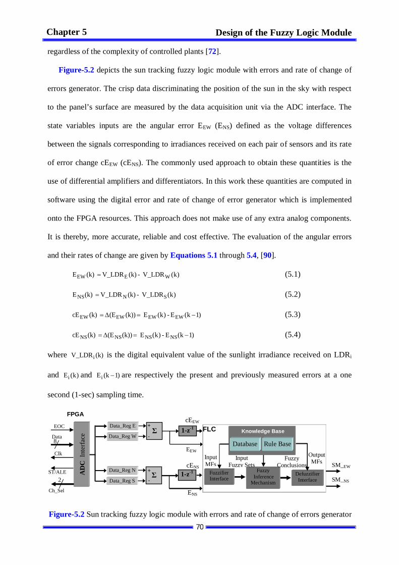
70
Design of the Fuzzy Logic Module
Chapter 5
regardless of the complexity of controlled plants [72].
Figure-5.2 depicts the sun tracking fuzzy logic module with errors and rate of change of
errors generator. The crisp data discriminating the position of the sun in the sky with respect
to the panel’s surface are measured by the data acquisition unit via the ADC interface. The
state variables inputs are the angular error EEW (ENS) defined as the voltage differences
between the signals corresponding to irradiances received on each pair of sensors and its rate
of error change cEEW (cENS). The commonly used approach to obtain these quantities is the
use of differential amplifiers and differentiators. In this work these quantities are computed in
software using the digital error and rate of change of error generator which is implemented
onto the FPGA resources. This approach does not make use of any extra analog components.
It is thereby, more accurate, reliable and cost effective. The evaluation of the angular errors
and their rates of change are given by Equations 5.1 through 5.4, [90].
)k(V_LDR - (k)V_LDR (k)E WEEW (5.1)
)k(V_LDR - (k)V_LDR (k)E SNNS (5.2)
)1k(E - )k(E (k))(E (k)cE EWEWEWEW (5.3)
)1k(E - )k(E (k))(E (k)cE NSNSNSNS (5.4)
where (k)V_LDRi is the digital equivalent value of the sunlight irradiance received on LDRi
and )k(Ei and )1k(Ei are respectively the present and previously measured errors at a one
second (1-sec) sampling time.
FPGA
1-z-1
EEW
cEEW
ENS
cENS
1-z-1
+
-
FLC
Fuzzifier Interface
Fuzzy Inference
Mechanism
Input Fuzzy Sets SM_EW
SM_NS
Database
Rule Base
Defuzzifier Interface
Knowledge Base
Input MFs
Fuzzy Conclusions
Output MFs
AD
C I
nter
face
Data_Reg N
Data_Reg S
8
2
EOC
ST/ALE
Data
Clk
Data_Reg E
Data_Reg W
Ch_Sel
+
-
Figure-5.2 Sun tracking fuzzy logic module with errors and rate of change of errors generator

71
Design of the Fuzzy Logic Module
Chapter 5
The fuzzy logic controller design flow consists of the following steps:
- Identify the input state variables and the ranges spanned by each variable.
- Identify the output variables and the ranges spanned by each one.
- Choose appropriate scaling factor for the input variables in order to normalize the variables
to the [0, 1] or [-1, 1] interval.
- The shapes of membership functions have to be fixed.
- The number of membership functions and their locations on the universe of discourse has to
be determined for every input state variable.
- Assign a linguistic label to each membership function
- Create the degree of fuzzy membership function for each variable
- Construct the rule base
- Use fuzzy approximate reasoning to infer the output contributed from each rule.
- Aggregate the fuzzy outputs recommended by each rule.
- Apply defuzzification to form a crisp output
- Choose appropriate post-processing to suite the crisp output of defuzzification module into
actual inputs for the process.
4 The Azimuth Fuzzy Logic Controller
The state variable inputs of the azimuth fuzzy-like PD-type controller are the angular error
EEW and its rate of change of error cEEW. The universe of discourse for the azimuth angular
error is defined as the maximum deviation from the optimal position of the solar panel with
respect to sun rays. Figure-5.3 illustrates the sun vector hitting a solar panel. The incident
angle is zero when sun rays are normal to the solar panel’s surface. This angle can range
from -90° at sunrise to +90° at sunset.
+90° -90° West East
Figure-5.3 Incident angle of sunrays with solar panel surface
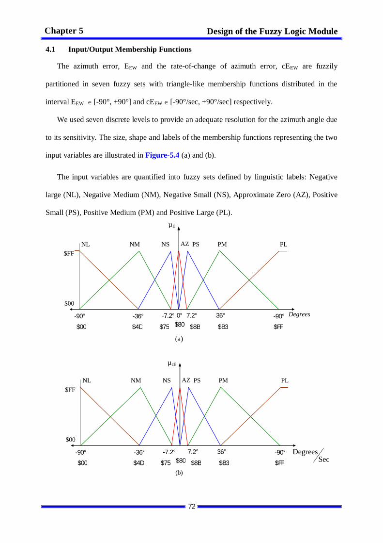
72
Design of the Fuzzy Logic Module
Chapter 5
4.1 Input/Output Membership Functions
The azimuth error, EEW and the rate-of-change of azimuth error, cEEW are fuzzily
partitioned in seven fuzzy sets with triangle-like membership functions distributed in the
interval EEW [-90°, +90°] and cEEW [-90°/sec, +90°/sec] respectively.
We used seven discrete levels to provide an adequate resolution for the azimuth angle due
to its sensitivity. The size, shape and labels of the membership functions representing the two
input variables are illustrated in Figure-5.4 (a) and (b).
The input variables are quantified into fuzzy sets defined by linguistic labels: Negative
large (NL), Negative Medium (NM), Negative Small (NS), Approximate Zero (AZ), Positive
Small (PS), Positive Medium (PM) and Positive Large (PL).
$00 $4D $75 $80 $B3 $8B
NL NM PL NS AZ PS PM
0° -90° 36° 7.2° -90° -7.2° -36°
$FF
Degrees
µE
$FF
$00
(a)
SecDegrees
$00 $4D $75 $80 $B3 $8B
NL NM PL NS AZ PS PM
-90° 36° 7.2° -90° -7.2° -36°
$FF
µcE
$FF
$00
(b)
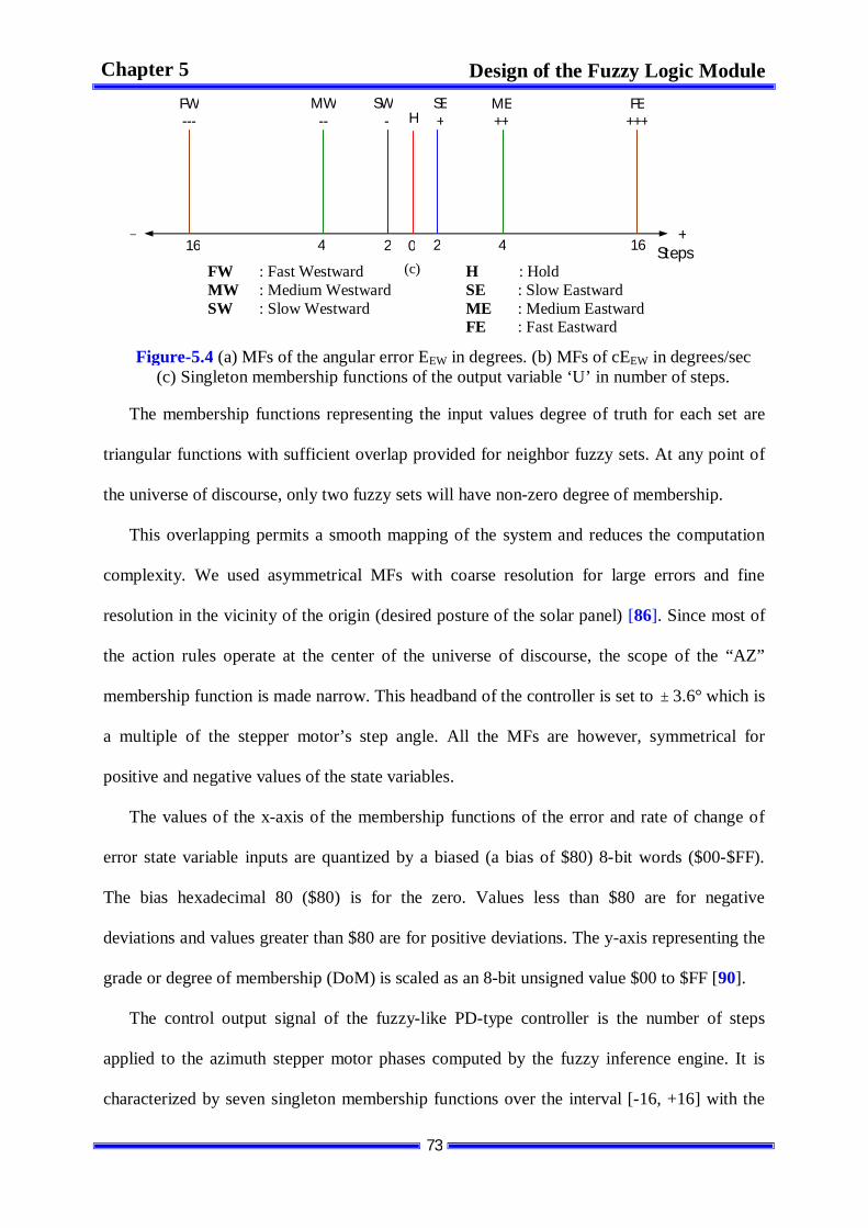
73
Design of the Fuzzy Logic Module
Chapter 5
The membership functions representing the input values degree of truth for each set are
triangular functions with sufficient overlap provided for neighbor fuzzy sets. At any point of
the universe of discourse, only two fuzzy sets will have non-zero degree of membership.
This overlapping permits a smooth mapping of the system and reduces the computation
complexity. We used asymmetrical MFs with coarse resolution for large errors and fine
resolution in the vicinity of the origin (desired posture of the solar panel) [86]. Since most of
the action rules operate at the center of the universe of discourse, the scope of the “AZ”
membership function is made narrow. This headband of the controller is set to 3.6° which is
a multiple of the stepper motor’s step angle. All the MFs are however, symmetrical for
positive and negative values of the state variables.
The values of the x-axis of the membership functions of the error and rate of change of
error state variable inputs are quantized by a biased (a bias of $80) 8-bit words ($00-$FF).
The bias hexadecimal 80 ($80) is for the zero. Values less than $80 are for negative
deviations and values greater than $80 are for positive deviations. The y-axis representing the
grade or degree of membership (DoM) is scaled as an 8-bit unsigned value $00 to $FF [90].
The control output signal of the fuzzy-like PD-type controller is the number of steps
applied to the azimuth stepper motor phases computed by the fuzzy inference engine. It is
characterized by seven singleton membership functions over the interval [-16, +16] with the
Figure-5.4 (a) MFs of the angular error EEW in degrees. (b) MFs of cEEW in degrees/sec (c) Singleton membership functions of the output variable ‘U’ in number of steps.
16 4 2 2 4 16 0
FW ---
MW --
FE +++
SW - H
SE +
ME ++
+ ¯ Steps
(c) FW : Fast Westward H : Hold MW : Medium Westward SE : Slow Eastward SW : Slow Westward ME : Medium Eastward FE : Fast Eastward
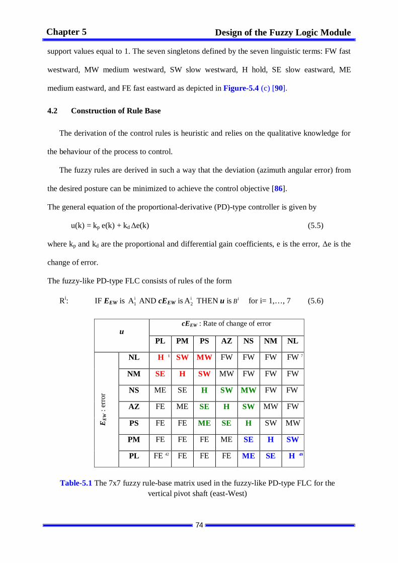
74
Design of the Fuzzy Logic Module
Chapter 5
support values equal to 1. The seven singletons defined by the seven linguistic terms: FW fast
westward, MW medium westward, SW slow westward, H hold, SE slow eastward, ME
medium eastward, and FE fast eastward as depicted in Figure-5.4 (c) [90].
4.2 Construction of Rule Base
The derivation of the control rules is heuristic and relies on the qualitative knowledge for
the behaviour of the process to control.
The fuzzy rules are derived in such a way that the deviation (azimuth angular error) from
the desired posture can be minimized to achieve the control objective [86].
The general equation of the proportional-derivative (PD)-type controller is given by
u(k) = kp e(k) + kd e(k) (5.5)
where kp and kd are the proportional and differential gain coefficients, e is the error, e is the
change of error.
The fuzzy-like PD-type FLC consists of rules of the form
Ri: IF EEW is i1A AND cEEW is i
2A THEN u is iB for i= 1,…, 7 (5.6)
cEEW : Rate of change of error u
PL PM PS AZ NS NM NL
NL H 1 SW MW FW FW FW FW 7
NM SE H SW MW FW FW FW
NS ME SE H SW MW FW FW
AZ FE ME SE H SW MW FW
PS FE FE ME SE H SW MW
PM FE FE FE ME SE H SW
EEW
: er
ror
PL FE 42 FE FE FE ME SE H 49
Table-5.1 The 7x7 fuzzy rule-base matrix used in the fuzzy-like PD-type FLC for the vertical pivot shaft (east-West)

75
Design of the Fuzzy Logic Module
Chapter 5
where is i1A and i
2A are the linguistic values representing the i-th antecedent pairs and the iB
is the fuzzy set representing the i-th conclusion.
Since both state variable inputs have seven MFs, then the total number of non-conflicting
fuzzy if-then rules is 7x7 = 49.
Table-5.1 summarizes these rules for the azimuth angle fuzzy-like PD type FLC in a
matrix form. The control rules are best visualized as a 2-dimentional matrix structure where
the most left column and the top row contain the fuzzy sets of the two antecedents EEW and
cEEW respectively. The fuzzy sets of the output control action are shown in the body of the
matrix.
The matrix can be partitioned into several subgroups. The central part of which for
example describes the situation where the azimuth angular error and its rate of change are
both either small or null, i.e., the misalignment is very small. Therefore, the control action to
correct this error should be null (H) or small in magnitude ((+) or (-)). In the situation where
the panel surface is too far from the desire posture (negative large or positive large), then, if
the rate of change of error is of the same sign, fast control action is provided ((+++) or (---))
to position the panel. The latter situations are illustrated by the upper right and lower left
corners. Referring to the rule base matrix, the physical meanings of some rules are described
below.
Rule 7: IF EEW is NL AND cEEW is NL THEN u is FW
The statement “angular error is negative large” represents the situation where LDRW receives
significantly more sunlight than LDRE, and “change in error (cEEW) is negative large” can
represent the situation where the tracker is moving eastward. Therefore, to track the sun, the
controller must apply a large control action “fast westward” to move the tracker westward.
Rule 25: IF EEW is AZ AND cEEW is AZ THEN u is H
This rule describes the situation the deviation is within the fuzzy AZ zone, and in the presence

76
Design of the Fuzzy Logic Module
Chapter 5
of a rate of change of error within the same zone, then, the controller holds current situation,
meaning that the sun is tracked.
Rule 32: IF EEW is PS AND cEEW is AZ THEN u is SE
The statement “if azimuth error is positive small AND change in error is nearly zero”
represents the situation where the solar panel is slightly misaligned eastward and since the
change in error is nearly zero, then the controller should move the panel slightly estward,
“slow eastward”.
Rule 49: IF EEW is PL AND cEEW is NL THEN u is H
This rule quantifies the situation where the panel is misaligned with the eastern LDR
receiving more sunlight than the western one. And because, the rate of change of the error is
large and of opposite sign, then, it is not necessary to apply any action, the tracker will end up
tracking the sun (self-correcting situation).
The matrix presents noticeable features. It has a skew symmetric property, that is, the
eastward linguistic values (SE, ME and FE) of the control action are placed below the
diagonal whereas the westward linguistic values (SW, MW and FW) are above the diagonal
with a hold control action placed along the diagonal (H). Another feature of this matrix is that,
in either direction, the number of steps to be applied for the actuators increases with
increasing distance from the diagonal.
The parameters characterizing the azimuth FLC are as follows:
1. Number of inputs: 2
2. Antecedent MFs seven triangular per fuzzy set
3. Output 1
4. Consequent MFs seven singletons
5. Maximum number of rules 49
6. Inference method max-min
7. Defuzzification COGS
77
Design of the Fuzzy Logic Module
Chapter 5
5 The Elevation Fuzzy Logic Controller
The second FLC adjusts the tilt angle of the tracker. It runs in parallel with the azimuth
angle controller. The inputs to this fuzzy controller are the elevation deviation or ENS and the
rate of change of error cENS. The output is the control action that drives the second stepper
motor.
The declination angle is the angle made by the line joining the centers of the sun and the
earth with its projection on the equatorial plane and it varies from -23.45° to +23.45°.
Because the change is on seasonal basis only, we provided a smaller number of quantization
level by partitioning the [-23.45°, +23.45°] universe of discourse using five triangle shaped
MFs. The linguistic terms used are: NL, NS, AZ, PS and PL. The driving force has five
singleton MFs: FN, SN, H, SS, and FS.
Figure-5.5 depicts the graphical representation of the MFs of the elevation error and
its rate of change.
(a) $00 $75 $80 $FF $8B
NL NS AZ PS PL
0° 25.2° 7.2° -7.2° -25.2° Degrees
µE
$FF
$00 ¯ +
(b) $00 $75 $80 $FF $8B
NL NS AZ PS PL
0° 25.2° 7.2° -7.2° -25.2° Degrees/sec
µcE
$FF
$00 + ¯
78
Design of the Fuzzy Logic Module
Chapter 5
Table-5.2 summarizes these rules for the elevation angle fuzzy-like PD type FLC in a
matrix form. The control rules are best visualized as a 2-dimentional matrix structure where
the most left column and the top row indicate the fuzzy sets of the two antecedents ENS and
cENS respectively. The fuzzy sets of the output control action are shown in the body of the
matrix.
Similar to the rule base matrix of the azimuth fuzzy controller, the rule base of the
elevation fuzzy controller also exhibits a skew symmetric property, that is, the northward
linguistic values (SN and FN) of the control action are placed below the diagonal whereas the
southward linguistic values (SS and FS) are above the diagonal with a hold control action
placed along the diagonal (H). Another feature of this matrix is that, in either direction, the
number of steps to be applied for the actuators increases with increasing distance from the
diagonal.
cENS : Rate of change of errorNS
PL PS AZ NS NL
NL H SS FS FS FS
NS SN H SS FS FS
AZ FN SN H SS FS
PS FN FN SN H SS E NS :
err
or
PL FN FN FN SN H
Steps 8 2 2 8 0
FS --
SS - H
SN +
FN ++
+ ¯ (c)
FS : Fast Southward SS : Slow Southward H : Hold SN : Slow Northward FN : Fast Northward
Figure-5.5 (a) MFs of the angular error ENS in degrees. (b) MFs of cENS in degrees/sec (c) Singleton membership functions of the output variable ‘U’ in number of steps.
Table-5.2 The 5x5 fuzzy rule-base matrix used in the fuzzy-like PD-type FLC for the horizontal pivot shaft (North-South)
1 5
25 21
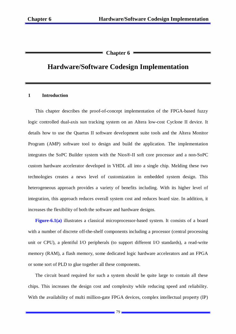
79
Hardware/Software Codesign Implementation Chapter 6
Chapter 6
Hardware/Software Codesign Implementation
1 Introduction
This chapter describes the proof-of-concept implementation of the FPGA-based fuzzy
logic controlled dual-axis sun tracking system on an Altera low-cost Cyclone II device. It
details how to use the Quartus II software development suite tools and the Altera Monitor
Program (AMP) software tool to design and build the application. The implementation
integrates the SoPC Builder system with the Nios®-II soft core processor and a non-SoPC
custom hardware accelerator developed in VHDL all into a single chip. Melding these two
technologies creates a news level of customization in embedded system design. This
heterogeneous approach provides a variety of benefits including. With its higher level of
integration, this approach reduces overall system cost and reduces board size. In addition, it
increases the flexibility of both the software and hardware designs.
Figure-6.1(a) illustrates a classical microprocessor-based system. It consists of a board
with a number of discrete off-the-shelf components including a processor (central processing
unit or CPU), a plentiful I/O peripherals (to support different I/O standards), a read-write
memory (RAM), a flash memory, some dedicated logic hardware accelerators and an FPGA
or some sort of PLD to glue together all these components.
The circuit board required for such a system should be quite large to contain all these
chips. This increases the design cost and complexity while reducing speed and reliability.
With the availability of multi million-gate FPGA devices, complex intellectual property (IP)
80
Hardware/Software Codesign Implementation Chapter 6
cores and soft core processors such as the Altera Nios® II, it is possible to contain a CPU,
I/Os, the dedicated custom hardware accelerator and the RAM all in a single FPGA chip,
Figure-6.1(b). The only component that we cannot put into the FPGA is the flash memory.
Integrating these devices on the same piece of silicon reduces cost and saves board space,
while it increases reliability and enhances anonymity and secrecy. Also, because the signals
between different components now reside on the same die, communication between them
consumes substantially less power. In addition, this integrated solution results in a
substantially higher bandwidth and lower latency compared to the former one.
2 FPGA Hardware Design Flow (SoPC Approach)
Designing and implementing embedded systems at system level targeting a
programmable logic platform such as the FPGA is impossible without sophisticated computer
aided design (CAD) tools. To cope with these complexities, Altera provides a Quartus II
software development tool which includes a SoPC Builder system integration tool to allow
designers to synthesize, simulate, program and debug their designs and build embedded
systems on Altera’s FPGA [91]. The remaining of this section, discusses the complete
hardware/software design flow for creating a SoPC Builder system with a custom logic
hardware accelerator (relevant details will be presented in forthcoming sections). Figure-6.2.
illustrates the FPGA hardware development design flow when using the SoPC approach.
Figure 6.1 Typical microprocessor-based system, (left) traditional method, (right) SoPC approach.
Processor Flash
SRAM
Custom Logic
Hardware
FPGA
I/O
I/O
I/O
I/O FPGA
Flash
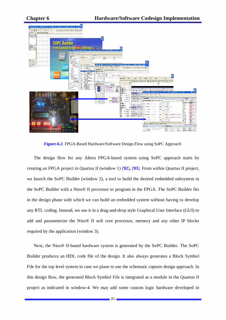
81
Hardware/Software Codesign Implementation Chapter 6
The design flow for any Altera FPGA-based system using SoPC approach starts by
creating an FPGA project in Quartus II (window 1) [92], [93]. From within Quartus II project,
we launch the SoPC Builder (window 2), a tool to build the desired embedded subsystem in
the SoPC Builder with a Nios® II processor to program in the FPGA. The SoPC Builder fits
in the design phase with which we can build an embedded system without having to develop
any RTL coding. Instead, we use it in a drag-and-drop style Graphical User Interface (GUI) to
add and parameterize the Nios® II soft core processor, memory and any other IP blocks
required by the application (window 3).
Next, the Nios® II-based hardware system is generated by the SoPC Builder. The SoPC
Builder produces an HDL code file of the design. It also always generates a Block Symbol
File for the top level system in case we plane to use the schematic capture design approach. In
this design flow, the generated Block Symbol File is integrated as a module in the Quartus II
project as indicated in window-4. We may add some custom logic hardware developed in
1
2
3
4
5
6
Figure-6.2. FPGA-Based Hardware/Software Design Flow using SoPC Approach

82
Hardware/Software Codesign Implementation Chapter 6
HDL or using schematic capture as non-SoPC Builder logic and interconnect it with the
Nios® II-based system. Next, we use Quartus II software to assign FPGA pin locations for the
input/output signals. A successful compilation of the project produces a programmable file,
the SRAM Object File (.sof), a file that determines the state of every programmable logic
element inside the FPGA. When the .sof file is downloaded using the Quartus II programmer
software, the FPGA on the development board is configured with the SoPC system hardware
(both the Nios® II-based subsystem and the custom core components). At this stage, it is
possible to perform a functional simulation (window-5).
The last step in the design flow is the development of the software program that we can
download and run on the Nios® II processor. In this work, Altera Monitor Program utility is
used to create in assembly language the firmware, compile, download and run the application
software program on the Nios® II (window 6).
3 Implementation of the Intelligent Sun Tracking Controller
Figure-6.3 depicts the conceptual top-level fuzzy control based dual-axis sun tracking
digital controller block diagram implemented in the Cyclone II FPGA using the System-on-a-
Programmable-Chip methodology. To reduce the complexity of the design process, the
structure of the hardware is partitioned into two subsystems: (i) an on-chip hardware module
implemented on the FPGA of the DE2 board. It encompasses the SoPC Builder system and
the non-SoPC modules. The SoPC Builder module includes the Nios® II based system with
all required peripherals and memory block. The non-SoPC system consists of custom clock
divider, a hardware accelerator the fuzzy logic module and the sequence generator all
developed in handcrafted VHDL and implemented on the FPGA fabric. (ii) An off-chip
hardware module implemented on a protoboard using discrete off-the-shelf analog and digital
components. It includes the sensing and data acquisition unit, the bidirectional voltage level
translator and the motor driving unit to energize the actuators.
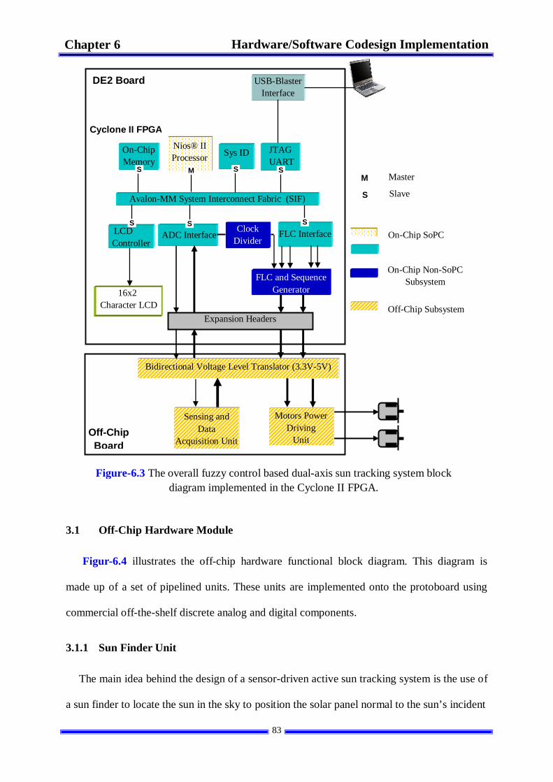
83
Hardware/Software Codesign Implementation Chapter 6
3.1 Off-Chip Hardware Module
Figur-6.4 illustrates the off-chip hardware functional block diagram. This diagram is
made up of a set of pipelined units. These units are implemented onto the protoboard using
commercial off-the-shelf discrete analog and digital components.
3.1.1 Sun Finder Unit
The main idea behind the design of a sensor-driven active sun tracking system is the use of
a sun finder to locate the sun in the sky to position the solar panel normal to the sun’s incident
16x2 Character LCD
Bidirectional Voltage Level Translator (3.3V-5V)
USB-Blaster Interface
Avalon-MM System Interconnect Fabric (SIF)
JTAG UART
Clock Divider
Cyclone II FPGA
Sys ID
LCD Controller
S
Nios® II Processor
M
On-Chip Memory
S S S
ADC Interface S
FLC Interface
FLC and Sequence Generator
Sensing and Data
Acquisition Unit
Motors Power Driving
Unit
S
M Master
Slave
On-Chip SoPC
On-Chip Non-SoPC Subsystem
Off-Chip Subsystem
S
Figure-6.3 The overall fuzzy control based dual-axis sun tracking system block diagram implemented in the Cyclone II FPGA.
DE2 Board
Expansion Headers
Off-Chip Board
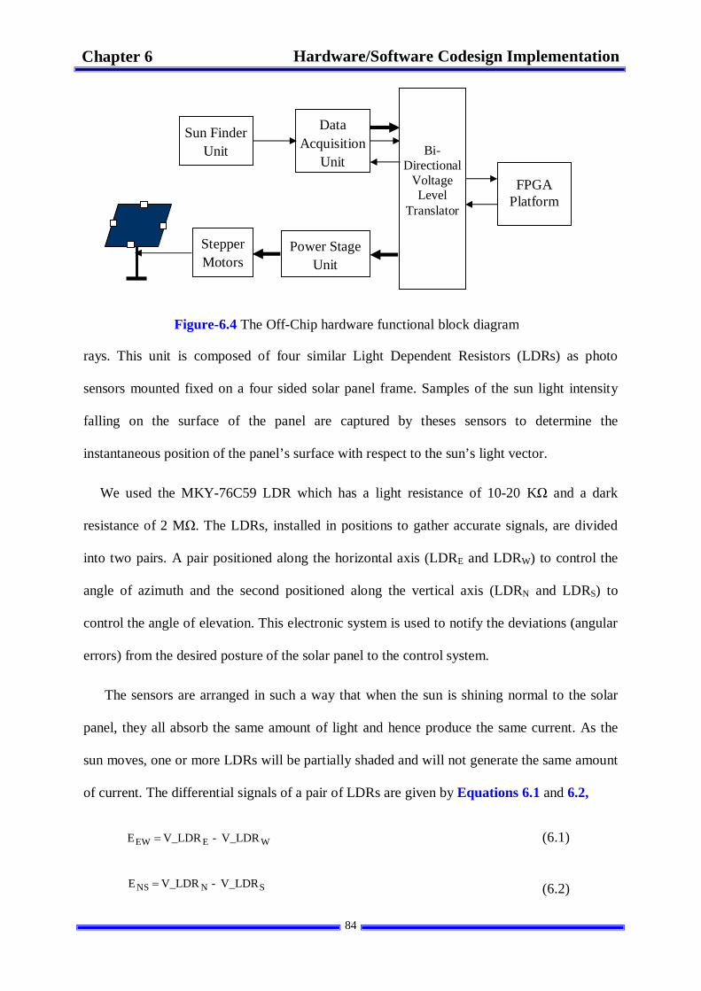
84
Hardware/Software Codesign Implementation Chapter 6
rays. This unit is composed of four similar Light Dependent Resistors (LDRs) as photo
sensors mounted fixed on a four sided solar panel frame. Samples of the sun light intensity
falling on the surface of the panel are captured by theses sensors to determine the
instantaneous position of the panel’s surface with respect to the sun’s light vector.
We used the MKY-76C59 LDR which has a light resistance of 10-20 K and a dark
resistance of 2 M . The LDRs, installed in positions to gather accurate signals, are divided
into two pairs. A pair positioned along the horizontal axis (LDRE and LDRW) to control the
angle of azimuth and the second positioned along the vertical axis (LDRN and LDRS) to
control the angle of elevation. This electronic system is used to notify the deviations (angular
errors) from the desired posture of the solar panel to the control system.
The sensors are arranged in such a way that when the sun is shining normal to the solar
panel, they all absorb the same amount of light and hence produce the same current. As the
sun moves, one or more LDRs will be partially shaded and will not generate the same amount
of current. The differential signals of a pair of LDRs are given by Equations 6.1 and 6.2,
WEEW V_LDR - V_LDR E (6.1)
SNNS V_LDR - V_LDR E (6.2)
FPGA Platform
Bi-Directional
Voltage Level
Translator
Data Acquisition
Unit
Sun Finder Unit
Power Stage Unit
Stepper Motors
Figure-6.4 The Off-Chip hardware functional block diagram

85
Hardware/Software Codesign Implementation Chapter 6
where the voltages EEW and ENS represent the angular errors of the azimuth and elevation
angles respectively and V_LDRi a voltage proportional to the intensity of light received by
LDRi. These errors are employed by the tracking controller to adjust the solar panel in order
to minimize these angular errors.
For example, when EEW is positive, it means that the eastern LDRE is receiving more
sunlight than the western LDRW. Therefore, the actuator driving the vertical pivot shaft
should rotate the solar panel eastward. Similarly, when ENS is negative the horizontal axis
driving actuator should rotate the panel southward. When the two errors are null the sun is
perfectly tracked.
3.1.2 Data Acquisition Unit
The sensing and data acquisition unit is the key requirement for the sun tracking system. It
provides the raw data to the processing unit. The real-time azimuth and elevation data are read
in via the analog-to-digital converter (ADC). These data are the sunlight intensity degrees
falling on the solar panel and sensed by the four LDRs.
A signal transformation circuit made up of a voltage divider and an operational
amplifier used as a unit gain buffer (to avoid loading effect) converts the “induced” resistance
value of the LDR into a voltage in the range 0 to 5 volts. This linear relationship between the
intensity of light and voltage values is suitable for the ADC. The LDR outputs are first
digitized by the converter before they are transferred through an input port to the Nios® II
based system. Figure-6.5 illustrates the circuit diagram of the sensing and data acquisition
unit interfaced to the Nios® II system via the ADC interface.
The ADC chip used in the system to digitize the detectors’ analog inputs is the National
ADC0808 a commercial low-cost converter. It is an 8-bit resolution successive-approximation
converter. The ADC0808 device has eight input channels allowing it to monitor up to eight-
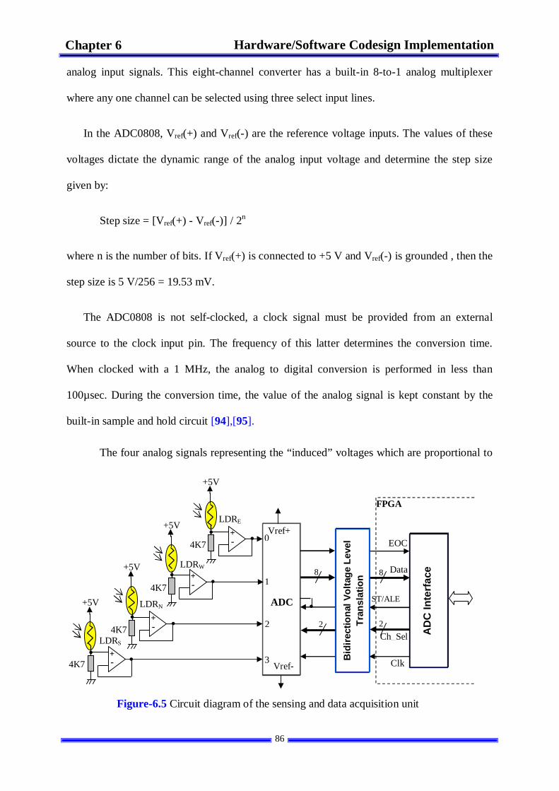
86
Hardware/Software Codesign Implementation Chapter 6
analog input signals. This eight-channel converter has a built-in 8-to-1 analog multiplexer
where any one channel can be selected using three select input lines.
In the ADC0808, Vref(+) and Vref(-) are the reference voltage inputs. The values of these
voltages dictate the dynamic range of the analog input voltage and determine the step size
given by:
Step size = [Vref(+) - Vref(-)] / 2n
where n is the number of bits. If Vref(+) is connected to +5 V and Vref(-) is grounded , then the
step size is 5 V/256 = 19.53 mV.
The ADC0808 is not self-clocked, a clock signal must be provided from an external
source to the clock input pin. The frequency of this latter determines the conversion time.
When clocked with a 1 MHz, the analog to digital conversion is performed in less than
100µsec. During the conversion time, the value of the analog signal is kept constant by the
built-in sample and hold circuit [94],[95].
The four analog signals representing the “induced” voltages which are proportional to
AD
C In
terf
ace
+5V
+ -
LDRS
0
3
1
2
8
2
EOC
Ch_Sel
Bid
irect
iona
l Vol
tage
Lev
el
Tran
slat
ion
ST/ALE
8
2
Data
Clk
+5V
+ -
LDRE
4K7
4K7
+5V
+ -
LDRN
4K7
+5V
+ -
LDRW
4K7 ADC
Figure-6.5 Circuit diagram of the sensing and data acquisition unit
Vref+
Vref-
FPGA
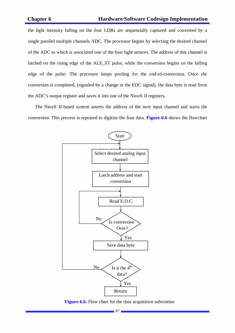
87
Hardware/Software Codesign Implementation Chapter 6
the light intensity falling on the four LDRs are sequentially captured and converted by a
single parallel multiple channels ADC. The processor begins by selecting the desired channel
of the ADC to which is associated one of the four light sensors. The address of this channel is
latched on the rising edge of the ALE_ST pulse, while the conversion begins on the falling
edge of the pulse. The processor keeps pooling for the end-of-conversion. Once the
conversion is completed, (signaled by a change in the EOC signal), the data byte is read from
the ADC’s output register and saves it into one of the Nios® II registers.
The Nios® II-based system asserts the address of the next input channel and starts the
conversion. This process is repeated to digitize the four data. Figure-6.6 shows the flowchart
Start
Select desired analog input channel
Is conversion Over?
Yes
No
Figure-6.6. Flow chart for the data acquisition subroutine
Latch address and start conversion
Read E.O.C
Save data byte
Is it the 4th data?
Return
No
Yes
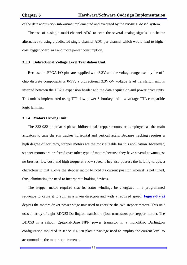
88
Hardware/Software Codesign Implementation Chapter 6
of the data acquisition subroutine implemented and executed by the Nios® II-based system.
The use of a single multi-channel ADC to scan the several analog signals is a better
alternative to using a dedicated single-channel ADC per channel which would lead to higher
cost, bigger board size and more power consumption.
3.1.3 Bidirectional Voltage Level Translation Unit
Because the FPGA I/O pins are supplied with 3.3V and the voltage range used by the off-
chip discrete components is 0-5V, a bidirectional 3.3V-5V voltage level translation unit is
inserted between the DE2’s expansion header and the data acquisition and power drive units.
This unit is implemented using TTL low-power Schottkey and low-voltage TTL compatible
logic families.
3.1.4 Motors Driving Unit
The 332-082 unipolar 4-phase, bidirectional stepper motors are employed as the main
actuators to tune the sun tracker horizontal and vertical axels. Because tracking requires a
high degree of accuracy, stepper motors are the most suitable for this application. Moreover,
stepper motors are preferred over other type of motors because they have several advantages:
no brushes, low cost, and high torque at a low speed. They also possess the holding torque, a
characteristic that allows the stepper motor to hold its current position when it is not tuned,
thus, eliminating the need to incorporate braking devices.
The stepper motor requires that its stator windings be energized in a programmed
sequence to cause it to spin in a given direction and with a required speed. Figure-6.7(a)
depicts the motors driver power stage unit used to energize the two stepper motors. This unit
uses an array of eight BDX53 Darlington transistors (four transistors per stepper motor). The
BDX53 is a silicon Epitaxial-Base NPN power transistor in a monolithic Darlington
configuration mounted in Jedec TO-220 plastic package used to amplify the current level to
accommodate the motor requirements.
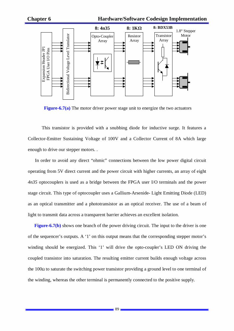
89
Hardware/Software Codesign Implementation Chapter 6
This transistor is provided with a snubbing diode for inductive surge. It features a
Collector-Emitter Sustaining Voltage of 100V and a Collector Current of 8A which large
enough to drive our stepper motors. .
In order to avoid any direct “ohmic” connections between the low power digital circuit
operating from 5V direct current and the power circuit with higher currents, an array of eight
4n35 optocouplers is used as a bridge between the FPGA user I/O terminals and the power
stage circuit. This type of optocoupler uses a Gallium-Arsenide- Light Emitting Diode (LED)
as an optical transmitter and a phototransistor as an optical receiver. The use of a beam of
light to transmit data across a transparent barrier achieves an excellent isolation.
Figure-6.7(b) shows one branch of the power driving circuit. The input to the driver is one
of the sequencer’s outputs. A ‘1’ on this output means that the corresponding stepper motor’s
winding should be energized. This ‘1’ will drive the opto-coupler’s LED ON driving the
coupled transistor into saturation. The resulting emitter current builds enough voltage across
the 100 to saturate the switching power transistor providing a ground level to one terminal of
the winding, whereas the other terminal is permanently connected to the positive supply.
Figure-6.7(a) The motor driver power stage unit to energize the two actuators
Bid
irect
iona
l Vol
tage
Lev
el T
rans
lato
r
Expa
nsio
n H
eade
r JP1
FP
GA
Use
r I/O
Pin
s
Transistor Array
Resistor Array
Opto-Coupler Array
8: 4n35 8: 1K 8: BDX53B 1.8° Stepper
Motor
90
Hardware/Software Codesign Implementation Chapter 6
1K
47
100
1K
+V From sequence
generator
Figure-6.7 (b). One branch (out of 8) of the driver power stage unit
Supply +V
91
Hardware/Software Codesign Implementation Chapter 6
3.2 On-Chip Hardware Module
The On-chip module is the bulk of the hardware system. This module consists of two
main parts: a SoPC Builder subsystem and an non-SoPC Builder subsystem. The former is
built around the Nios® II embedded soft processor, the latter is developed in handcrafted
VHDL as hardware accelerators. The overall module is implemented and ran on the Altera
Cyclone II EP2C35 low-cost FPGA clocked at 50 MHz and features a 33,216 LEs, 35
hardware multipliers, 4 phase-locked loops (PLLs) and up to 475 user I/O pins. Figure-6.8.
illustrates the overall on-chip hardware module.
3.2.1 On-Chip non-SoPC Builder Subsystem
This subsystem operates concurrently with the SoPC Builder subsystem to enhance
performance and reduces system complexity. It is made up of several units, all of which are
developed in VHDL.
3.2.1.1 The clock divider module
16x2 Character LCD
USB-Blaster Interface
Avalon-MM System Interconnect Fabric (SIF)
JTAG UART
Clock Divider
Cyclone II FPGA
Sys ID
LCD Controller
S
Nios® II Processor
M
On-Chip Memory
S S S
ADC Interface S
FLC Interface
FLC and Sequence Generator
S
M Master
Slave
SoPC Builder Subsystem
non-SoPC Builder Subsystem
S
Figure-6.8 The On-Chip hardware module
92
Hardware/Software Codesign Implementation Chapter 6
The clock divider module developed in VHDL, takes as input the 50 MHz master clock of
the DE2 board. It generates two clock signals: a 1 MHz clock signal suitable to trigger the
ADC and a 12 Hz, clock signal to trigger the stepper motors drive sequencers. Figure-6.9
illustrates the VHDL code to produce the required clock signals out of the DE2 board master
clock.
3.2.1.2 Implementation of the Fuzzy Logic Module
The fuzzy logic controller module described in chapter 5 is a custom hardware accelerator
developed in VHDL is interfaced to the Nios® II based system. Custom components designed
for intensive computation tasks are generally implemented in the FPGA fabric. The designer
can integrate these components “inside” or “outside” the SoPC Builder system. When
integrated “inside” the SoPC Builder system, it communicates with the other modules and the
processor through the Avalon Memory-Mapped interface. On the other hand, the custom
library ieee; use ieee.std_logic_1164.all; use ieee.std_logic_unsigned.all; entity Clk_Divider is port(clk: in std_logic; clk1, clk_ADC: out std_logic); end Clk_Divider; architecture behavioral of Clk_Divider is signal state1: std_logic_vector(5 downto 0); signal state2: std_logic_vector(26 downto 0); begin ADC: process(clk) begin if clk'event and clk = '1' then if state1 = 49 then state1 <= "000000"; else state1 <= state1 + 1; end if; end if; end process ADC; SM: process(clk) begin if clk'event and clk = '1' then state2 <= state2 + 1; end if; end process SM; clk_ADC <= state1(5); clk1 <= state2(22); end behavioral;
Figure 6.9 VHDL code of the clock divider custom hardware module
93
Hardware/Software Codesign Implementation Chapter 6
component can exist within the FPGA alongside the Nios® II based system, that is, “outside”
the SoPC Builder system. In this case, it can interact with the processor and other components
through parallel input-output interface adapters. The latter approach has the advantage of
having both custom cores and the Nios® processor execute concurrently, enhancing system
response. The purpose of having a processor co-exist with conventional digital logic
components is to provide flexibility of combining software and hardware based control in one
chip. Figure-6.10 depicts the synthesized schematic view of the fuzzy logic module in the
Quartus II register transfer level (RTL) Viewer tool.
3.2.1.3 Stepper Motor Sequence Generator
The stepper motor requires that its stator windings be energized in a programmed
sequence to generate a rotating magnetic field inside the motor, and the rotor will obediently
follow it. For the motor to develop higher torque, it is desirable to apply a full-step sequence
to its windings which involves powering two windings at one time. Figure-6.11 shows a
unipolar stepper motor windings and the full-step drive sequence.
Figure 6.10 A detailed view of the fuzzy logic module in Quartus II and the RTL Viewer
94
Hardware/Software Codesign Implementation Chapter 6
Figure-6.12 depicts the VHDL finite state machine implementation of the full-step driving
sequence.
Figure 6.12 VHDL code for a stepper motor full-step sequence generator.
Figure 6.11 Unipolar stepper motor windings and full-step sequence.
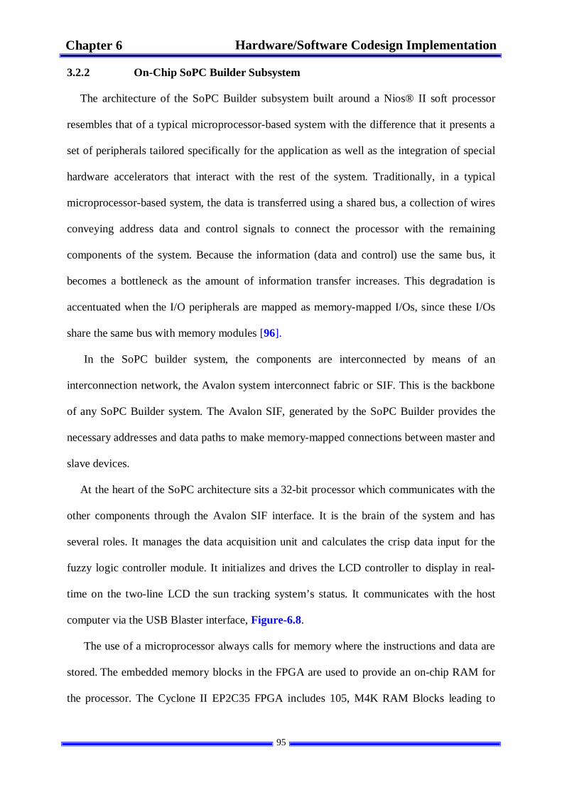
95
Hardware/Software Codesign Implementation Chapter 6
3.2.2 On-Chip SoPC Builder Subsystem
The architecture of the SoPC Builder subsystem built around a Nios® II soft processor
resembles that of a typical microprocessor-based system with the difference that it presents a
set of peripherals tailored specifically for the application as well as the integration of special
hardware accelerators that interact with the rest of the system. Traditionally, in a typical
microprocessor-based system, the data is transferred using a shared bus, a collection of wires
conveying address data and control signals to connect the processor with the remaining
components of the system. Because the information (data and control) use the same bus, it
becomes a bottleneck as the amount of information transfer increases. This degradation is
accentuated when the I/O peripherals are mapped as memory-mapped I/Os, since these I/Os
share the same bus with memory modules [96].
In the SoPC builder system, the components are interconnected by means of an
interconnection network, the Avalon system interconnect fabric or SIF. This is the backbone
of any SoPC Builder system. The Avalon SIF, generated by the SoPC Builder provides the
necessary addresses and data paths to make memory-mapped connections between master and
slave devices.
At the heart of the SoPC architecture sits a 32-bit processor which communicates with the
other components through the Avalon SIF interface. It is the brain of the system and has
several roles. It manages the data acquisition unit and calculates the crisp data input for the
fuzzy logic controller module. It initializes and drives the LCD controller to display in real-
time on the two-line LCD the sun tracking system’s status. It communicates with the host
computer via the USB Blaster interface, Figure-6.8.
The use of a microprocessor always calls for memory where the instructions and data are
stored. The embedded memory blocks in the FPGA are used to provide an on-chip RAM for
the processor. The Cyclone II EP2C35 FPGA includes 105, M4K RAM Blocks leading to
96
Hardware/Software Codesign Implementation Chapter 6
483,840 total RAM bits. The Join Test Action Group Universal Asynchronous
Receiver/Transmitter (JTAG-UART) interface is used to provide a Universal Serial Bus
(USB) link between the FPGA platform and the host computer. This circuitry and the
associated software are called the USB-Blaster [92].
We also added a system ID peripheral. This component provides the SoPC Builder system
with a unique identifier and therefore, safeguards it against any accidental downloading
software compiled for a different Nios® II system. To drive the 16x2 character liquid crystal
display (LCD) peripheral, we used a SoPC Builder LCD controller component.
The ADC interface module includes several parallel input-output peripherals tailored to
accommodate different signals of the off-chip data acquisition unit. This later unit constructed
around a low-cost multiple-channel analog-to-digital converter is used to sample the current
position of the sun in the sky via four light dependent resistors (LDRs). The dark blue blocks:
the clock divider and the FLC and the stepper motor sequence generator are the custom
hardware logic blocks.
3.2.3 Building the Embedded System in the SoPC Builder
The SoPC Builder, part of the Quartus II software, is a powerful hardware generation tool.
It streamlines the process of integrating blocks of IPs and accelerates development of system-
on-a-programmable-chip designs compared to traditional, manual integration methods. The
tool was introduced by Altera to design systems at block level. It consists of two major parts:
a graphical user interface or GUI and a system generator program [93].
Figure-6.13 shows a screenshot of the sun tracking controller optimized in an FPGA. The
GUI consists of several parts. The window on the left side is the library of available pre-made
IP cores (including the flagship Nios® II soft core processor) from which the designer picks
up the desired components required by the application.
97
Figure-6.13 SoPC-based intelligent sun tracking controller optimized in an FPGA.
98
Hardware/Software Codesign Implementation Chapter 6
We construct the embedded SoPC Builder system in the Avalon framework. The
construction of the system is accomplished by means of a drag-and-drop style. The required
components are dragged and parameterized in the contents page (the central window). The
“Module Name” and “Description” columns show the names and interfaces of the configured
intellectual property (IP) cores used in the application. The “connections” column in Figure-
6.13 is the interconnect logic.
Finally, the beginning and end of the memory addresses of the various components used
in the design are shown under “Base” and “End” columns. Because the Nios® II processor
maps the I/O peripherals as memory-mapped I/O, then the 32-bit address space is assigned to
both the memory component and to the I/O peripherals. In general, to avoid any conflicts for
all these memory-mapped components, it is more convenient to automatically assign these
unique base addresses.
The ADC interface is implemented with four parallel input-output interface adapters
(PIOs) of different dimensions. They are:
ADC: The first PIO configured as an 8-bit input port to route the digital data from the
converter to the processor when the conversion is completed.
Channel_Select: The second PIO tailored as a 2-bit output port. This output port drives the
two least significant address lines of the converter to select any one of
the four channels.
Start_Conversion: The third PIO is a 1-bit output port. The processor outputs a positive
pulse through this port to accomplish two functions. It latches the address of the
selected channel on the positive edge of the pulse and starts the conversion on the
negative edge of the pulse.
EOC: This last PIO is specified as a 1-bit input port. It is used to route the end-of-conversion
output signal of the analog-to-digital converter to be polled by the microprocessor.
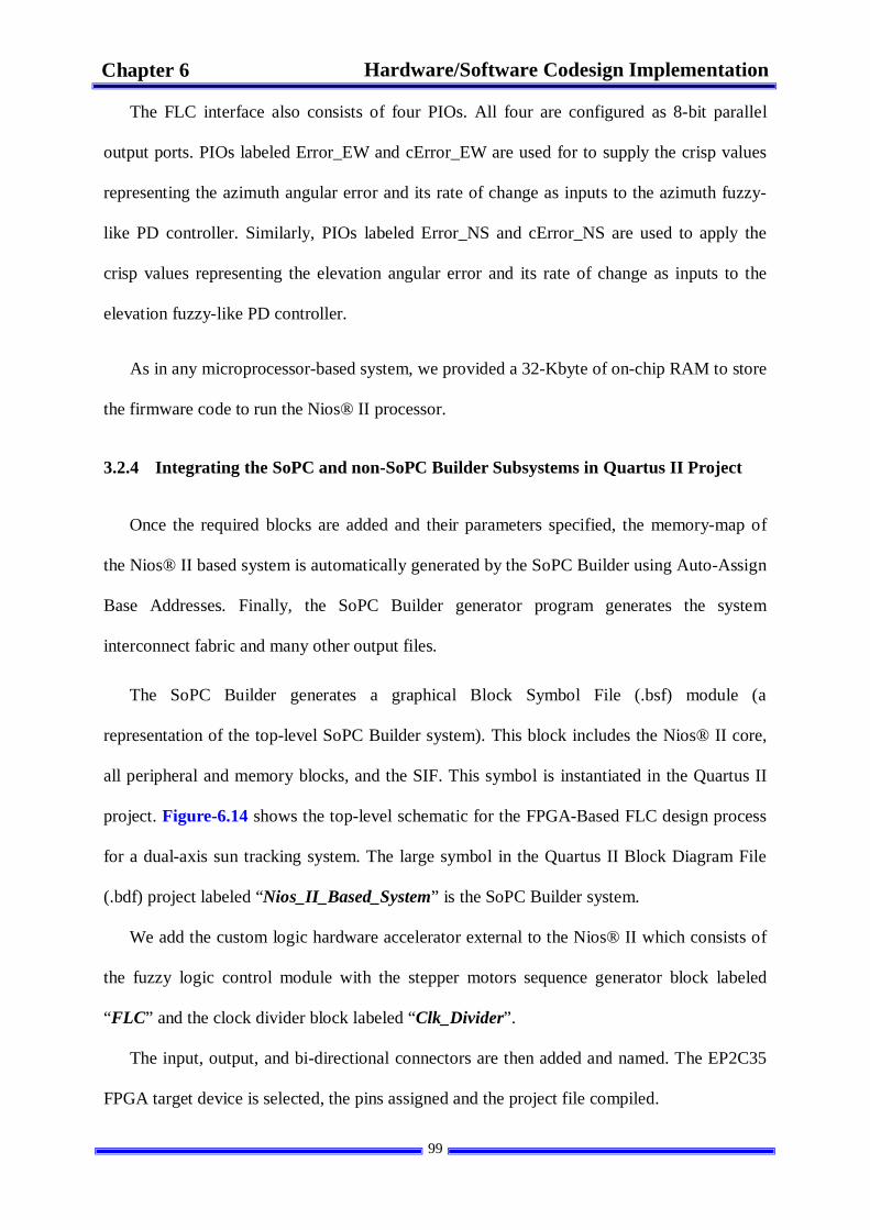
99
Hardware/Software Codesign Implementation Chapter 6
The FLC interface also consists of four PIOs. All four are configured as 8-bit parallel
output ports. PIOs labeled Error_EW and cError_EW are used for to supply the crisp values
representing the azimuth angular error and its rate of change as inputs to the azimuth fuzzy-
like PD controller. Similarly, PIOs labeled Error_NS and cError_NS are used to apply the
crisp values representing the elevation angular error and its rate of change as inputs to the
elevation fuzzy-like PD controller.
As in any microprocessor-based system, we provided a 32-Kbyte of on-chip RAM to store
the firmware code to run the Nios® II processor.
3.2.4 Integrating the SoPC and non-SoPC Builder Subsystems in Quartus II Project
Once the required blocks are added and their parameters specified, the memory-map of
the Nios® II based system is automatically generated by the SoPC Builder using Auto-Assign
Base Addresses. Finally, the SoPC Builder generator program generates the system
interconnect fabric and many other output files.
The SoPC Builder generates a graphical Block Symbol File (.bsf) module (a
representation of the top-level SoPC Builder system). This block includes the Nios® II core,
all peripheral and memory blocks, and the SIF. This symbol is instantiated in the Quartus II
project. Figure-6.14 shows the top-level schematic for the FPGA-Based FLC design process
for a dual-axis sun tracking system. The large symbol in the Quartus II Block Diagram File
(.bdf) project labeled “Nios_II_Based_System” is the SoPC Builder system.
We add the custom logic hardware accelerator external to the Nios® II which consists of
the fuzzy logic control module with the stepper motors sequence generator block labeled
“FLC” and the clock divider block labeled “Clk_Divider”.
The input, output, and bi-directional connectors are then added and named. The EP2C35
FPGA target device is selected, the pins assigned and the project file compiled.
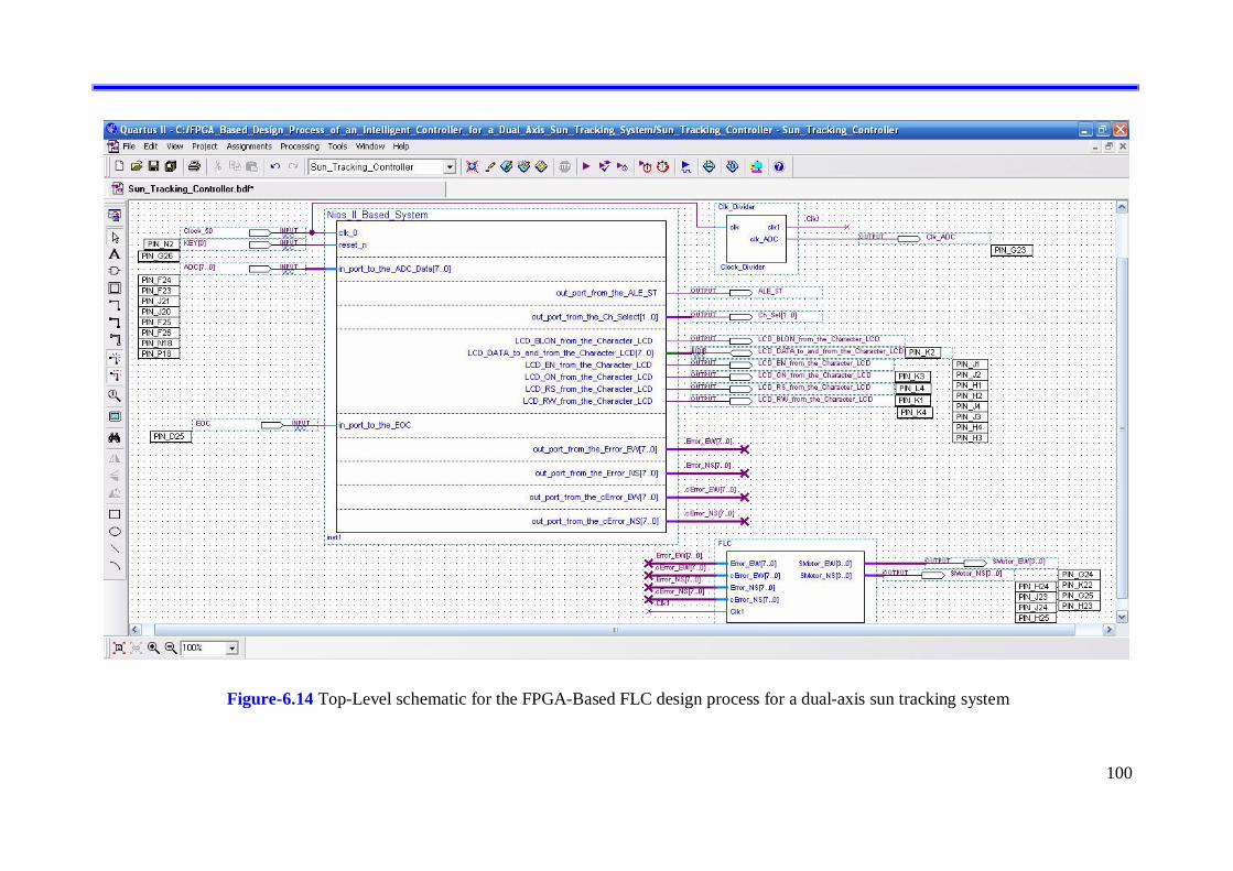
100
Figure-6.14 Top-Level schematic for the FPGA-Based FLC design process for a dual-axis sun tracking system
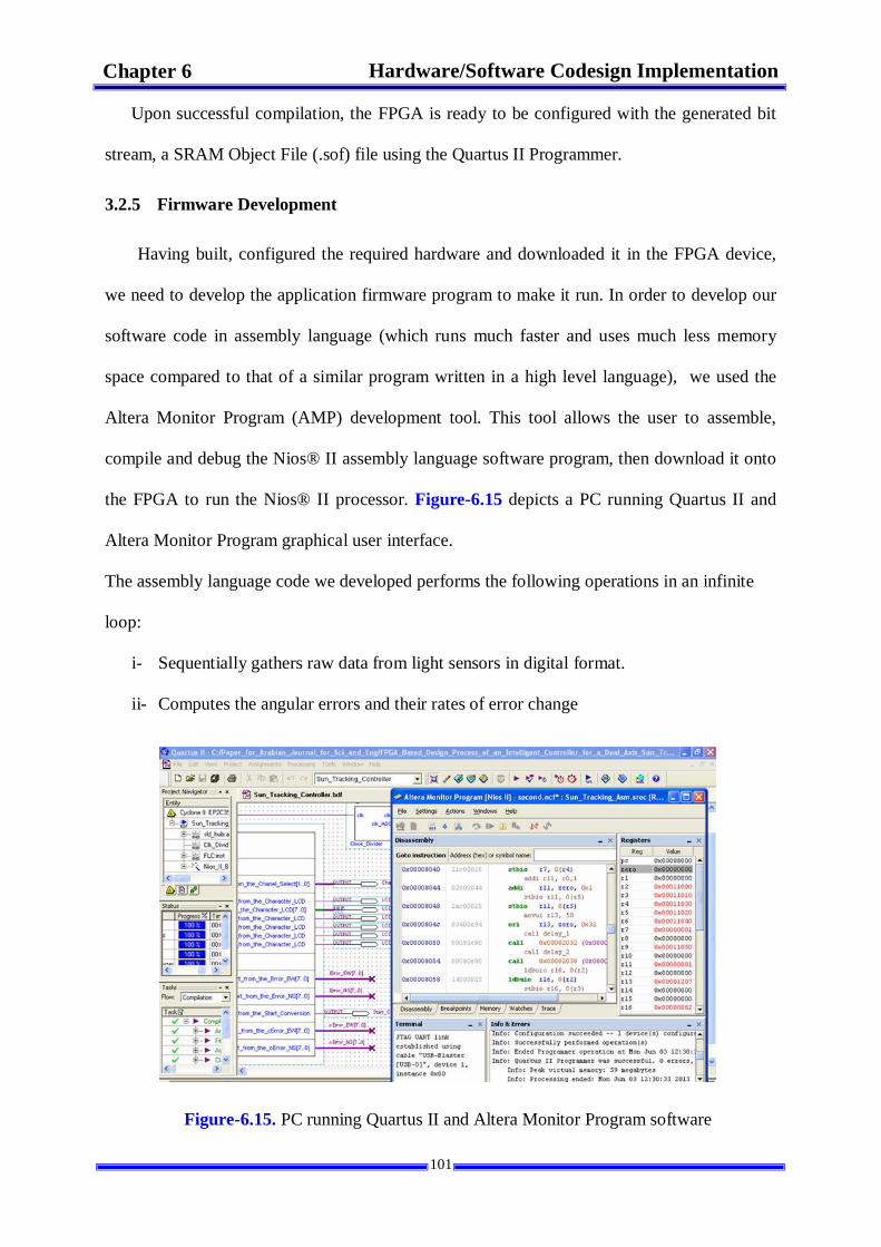
101
Hardware/Software Codesign Implementation Chapter 6
Upon successful compilation, the FPGA is ready to be configured with the generated bit
stream, a SRAM Object File (.sof) file using the Quartus II Programmer.
3.2.5 Firmware Development
Having built, configured the required hardware and downloaded it in the FPGA device,
we need to develop the application firmware program to make it run. In order to develop our
software code in assembly language (which runs much faster and uses much less memory
space compared to that of a similar program written in a high level language), we used the
Altera Monitor Program (AMP) development tool. This tool allows the user to assemble,
compile and debug the Nios® II assembly language software program, then download it onto
the FPGA to run the Nios® II processor. Figure-6.15 depicts a PC running Quartus II and
Altera Monitor Program graphical user interface.
The assembly language code we developed performs the following operations in an infinite
loop:
i- Sequentially gathers raw data from light sensors in digital format.
ii- Computes the angular errors and their rates of error change
Figure-6.15. PC running Quartus II and Altera Monitor Program software
102
Hardware/Software Codesign Implementation Chapter 6
iii- Feeds the PD-like FLC with the computed data
iv- Displays system’ status on the LCD to provide feedback to the user
v- Enters into a delay loop, a time during which the FLC determines the action to be
carried on to position the solar panel at its optimal posture.
vi- Repeat.
4 Real-Time Experiment
The overall apparatus of the prototyping platform built in the laboratory for testing and
verifying the intelligent dual-axis sun tracking system is illustrated in Figure-6.16. (a), (b). It
depicts both the off-chip hardware system on the protoboards and the on-chip
hardware/software co-design system on the FPGA board (DE2). The FPGA containing the
hardware implementation of the digital controller controls the off-chip hardware circuitry via
the board’s expansion header. The expansion header provides general-purpose input/output
(GPIO) pins. These GPIOs are directly connected to the FPGA device. It is also linked by
means of the USB Blaster mechanism to the PC running Altera monitor program and Quartus
II software develepment suite tools. The remaining parts of the prototype consists of a dual-
axis tracker platform with a sun finder.
Elevation Axis
Azimuth Pivot
DE2 Board
Figure-6.16. (a). Hardware setup of the FPGA-based intelligent dual-axis sun tracking system.
PC Running Quartus II
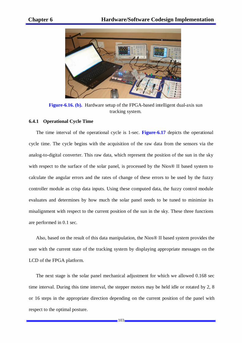
103
Hardware/Software Codesign Implementation Chapter 6
6.4.1 Operational Cycle Time
The time interval of the operational cycle is 1-sec. Figure-6.17 depicts the operational
cycle time. The cycle begins with the acquisition of the raw data from the sensors via the
analog-to-digital converter. This raw data, which represent the position of the sun in the sky
with respect to the surface of the solar panel, is processed by the Nios® II based system to
calculate the angular errors and the rates of change of these errors to be used by the fuzzy
controller module as crisp data inputs. Using these computed data, the fuzzy control module
evaluates and determines by how much the solar panel needs to be tuned to minimize its
misalignment with respect to the current position of the sun in the sky. These three functions
are performed in 0.1 sec.
Also, based on the result of this data manipulation, the Nios® II based system provides the
user with the current state of the tracking system by displaying appropriate messages on the
LCD of the FPGA platform.
The next stage is the solar panel mechanical adjustment for which we allowed 0.168 sec
time interval. During this time interval, the stepper motors may be held idle or rotated by 2, 8
or 16 steps in the appropriate direction depending on the current position of the panel with
respect to the optimal posture.
Figure-6.16. (b). Hardware setup of the FPGA-based intelligent dual-axis sun tracking system.
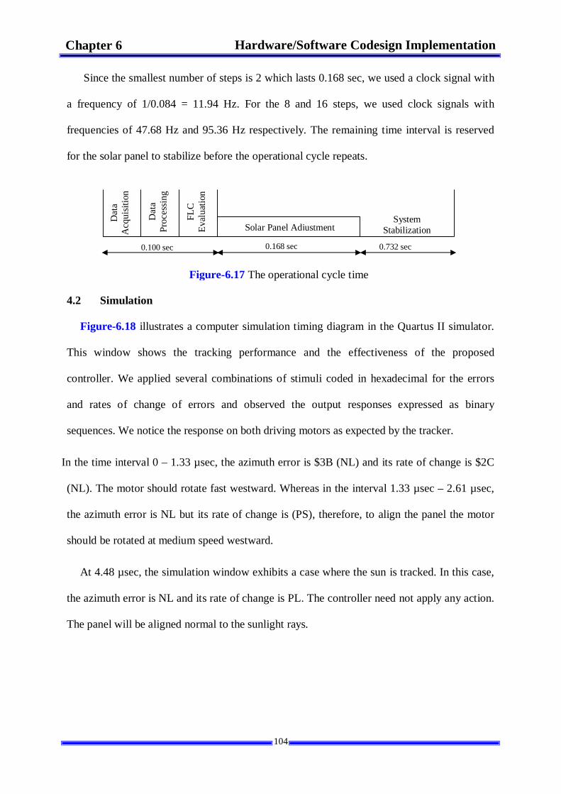
104
Hardware/Software Codesign Implementation Chapter 6
Since the smallest number of steps is 2 which lasts 0.168 sec, we used a clock signal with
a frequency of 1/0.084 = 11.94 Hz. For the 8 and 16 steps, we used clock signals with
frequencies of 47.68 Hz and 95.36 Hz respectively. The remaining time interval is reserved
for the solar panel to stabilize before the operational cycle repeats.
4.2 Simulation
Figure-6.18 illustrates a computer simulation timing diagram in the Quartus II simulator.
This window shows the tracking performance and the effectiveness of the proposed
controller. We applied several combinations of stimuli coded in hexadecimal for the errors
and rates of change of errors and observed the output responses expressed as binary
sequences. We notice the response on both driving motors as expected by the tracker.
In the time interval 0 – 1.33 µsec, the azimuth error is $3B (NL) and its rate of change is $2C
(NL). The motor should rotate fast westward. Whereas in the interval 1.33 µsec – 2.61 µsec,
the azimuth error is NL but its rate of change is (PS), therefore, to align the panel the motor
should be rotated at medium speed westward.
At 4.48 µsec, the simulation window exhibits a case where the sun is tracked. In this case,
the azimuth error is NL and its rate of change is PL. The controller need not apply any action.
The panel will be aligned normal to the sunlight rays.
Solar Panel Adjustment System
Stabilization
Dat
a
Acq
uisit
ion
Dat
a
Proc
essi
ng
FLC
Ev
alua
tion
0.100 sec 0.168 sec 0.732 sec
Figure-6.17 The operational cycle time
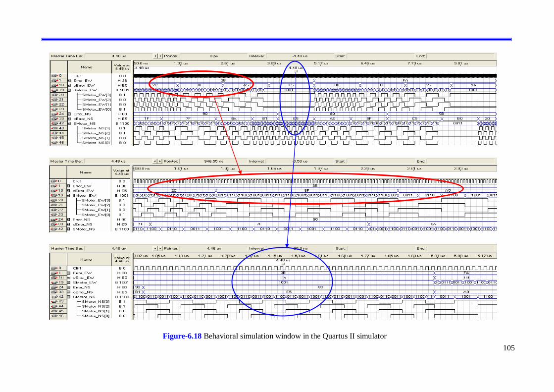
105
Figure-6.18 Behavioral simulation window in the Quartus II simulator
106
Conclusions Chapter 7
Chapter 7
Conclusions
In this thesis, we presented the design, simulation and implementation processes of a
customized FPGA-based (SoPC approach) applied to an intelligent sensor-driven dual-axis
sun tracking system in order to maximize power extraction from the solar panel. The goal of
using fuzzy control technology is to put human knowledge into engineering systems in a
systematic and efficient order. We designed our system with several considerations in mind:
autonomy, execution speed and cost, and design complexity. In this regard, the intelligent
controller is developed on an FPGA-based heterogeneous computing platform where the
overall controller is partitioned between two concurrent modules.
1- A fuzzy control module, as a hardware accelerator, implemented on the FPGA fabric
using VHDL is utilized to control the steering motors according to the deviation from
the desired (optimal) posture of the solar panel.
2- A Nios® II based system to acquire the raw data, compute the state variables of the
controller and displays in real-time the status of the overall system.
This hardware/software codesign implementation exploits the simplicity of the
microprocessor and the massively parallel architecture of the FPGA. This methodology
provides a high degree of flexibility in both hardware and software compared to classical

107
Conclusions Chapter 7
computing platforms. Other reasons why this approach is interesting: It works. It can be
applicable to almost all fields.
The SoPC approach has several advantages:
(1) It allows the use of the exact number of peripherals needed and the
parameterization of the peripherals to respond to the application.
(2) The reconfigurability nature of the FPGA and the short development cycle makes
it possible to perform modifications of any component of the system at any stage
of the implementation.
(3) To prevent from obsolescence, the design can be migrated into another larger and
more performant FPGA that does not exist yet.
(4) The ability to integrate an entire system on a single chip at a lower cost compared
to the use of off-the-shelf discrete components (MCU, DSP, ASSP, etc) solutions.
(5) The capability to off-load the computation-intensive functions from the software
application running on the soft processor and to implement them as hardware
accelerators in the FPGA fabric using VHDL or another design entry.
A common practice to obtain the inputs for the FLC is the use of differential amplifiers and
differentiators, in this work these parameters are computed within the FPGA using a digital
processing unit. This design greatly enhances system reliability and reduces chip count.
Moreover, the robustness of the FLC allows the use of cheaper sensors and low resolution
ADCs resulting in reduced implementation cost.
Further works
There are at least two possible directions to work on the way to improve further system
performance, design simplicity and flexibility.
(i) Integrating the fuzzy control module as an intellectual property (IP) component
with Avalon interface and connect it to the Avalon Memory Mapped interface.

108
Conclusions Chapter 7
(ii) Add custom instructions to the soft-core processor instruction set.
The use of the Nios® II software build tools (SBT) for eclipse to develop the application
software code in C, will further improve design productivity and lessen design complexity.
For extremely high speed applications, it is possible to sample all analog data
simultaneously using several high speed ADCs, a performance that cannot be achieved with
either the microcontroller of the DSP.
In the next generation of FPGAs, where ADCs will be built into the fabric of the FPGA,
the proposed computing platform will be more efficient in terms of hardware resources,
power consumption and control performance when compared with the standard MCU, DSP
solutions.
It is believed that with the significant advancements in materials and technologies
combined to the growing awareness concerning environmental problems, renewable energies
and solar in particular (with more than 60% annual average growth rate for the past five
years) are the future.
109
References References
References
[1] Z. Sen, “Solar energy in progress and future research trends.” Progress in Energy and
Combustion Science, 30, pp. 367-416, 2004.
[2] Saifur. Rahman, “Green Power. Where is it and where can we find it?” IEEE Power &
Energy magazine, Jan/Feb 2003. pp. 30-37.
[3] P. Fornasiero, M. Graziani, Renewable Resources and Renewable Energy: A Global
Challenge, 2nd Edition, Taylor & Francis, 2006.
[4] H. Scheer, The Solar Economy: Renewable Energy for a Sustainable Global Future,
Earthscan, 2004.
[5] AIA Research Corporation; “Solar Dwelling Design Concepts”. Washington, DC: U.S.
Government Printing Office, 1976.
[6] Y. Goswami, F. Kreith, and J. Kreder, “Principle of solar engineering,” in
Fundamentals of Solar Radiation, Philadephia, PA: Taylor & Francis, 1999.
[7] S. Seme, G. Stumberger, and J. Vorsic, “Maximum ef ciency trajectories of a two-
axis sun tracking system determined considering tracking system consumption”, IEEE
Trans. On Power Electronics, Vol. 26, No. 4, April 2011. pp. 1280-1290.
[8] C.Y. Lee, P. C. Chou, C. M. Chiang, and C.F. Lin, “Sun tracking systems: a review.”
Sensors. 9, pp. 3875-3890, 2009.
[9] K-K. Chong, C-W. Wong, F-L. Siaw, T-K. Yew, S-S Ng, M-S. Liang, Y-S. Lim and
S-L. Lau, “Integration of an On-Axis General Sun-Tracking Formula in the Algorithm
of an Open-Loop Sun-Tracking System”. Sensors, 9, pp. 7849-7865, 2009.
[10] R. Woods, J. McAllister, G. Lightbody and Ying Yi, FPGA-based Implementation of
signal processing systems, John Wiley & Sons, Ltd. 2008.
[11] Ian Grout, Digital Systems Design with FPGAs and CPLDs, 2008, Elsevier Ltd. ISBN-
13: 978-0-7506-8397-5
110
References References
[12] Altera, “Optimize system flexibility by integrating custom microprocessors into
FPGAs,” wp-aab090805-1.1, Fev-2006.
Available online at www.altera.com/literature/wp/wp-aab0900805.pdf
[13] Zekai Sen , “Solar energy in progress and future research trends”, Progress in Energy
and Combustion Science 30, 2004, pp. 367–416.
[14] T. Fazel, S. Zainal and M. A. Shahrin, “FPGA implementation of a single-input fuzzy
logic controller for boost converter with the absence of an external analog-to-Digital
converter.” IEEE Trans. On. Ind. Electronics, Vol.59, No.2, pp.1208-1217. Feb 2012.
[15] Yi Fu, L. Howard and M.E. Kaye, “Hardware/Software codesign for a fuzzy
autonomous road-following system.” IEEE Trans. On Systems, Man, and Cyber,
Vol.40, No.6, pp. 690-696. Nov-2010.
[16] A. H. Zavala and O. C. Nieto, “Fuzzy Hardware: a retrospective and analysis,” IEEE
Trans. On Fuzzy Systems, Vol.20, No. 4, August 2012. pp. 623-635.
[17] G. Bosque, I. del Campo and J. Echanobe, “Fuzzy systems, neural networks and
neuro-fuzzy systems: A vision on their hardware implementation and platforms over
two decades” Engineering App of Arti cial Intelligence 32, 2014, pp.283–331.
[18] A. Merlaud, M. De Mazière, C. Hermans, and A. Cornet, “Equations for solar
tracking.” Sensors. 12, pp.4074-4090, 2009.
[19] A. B. Sproul, “Derivation of the solar geometric relationships using vector analysis.”
Renewable Energy. Vol. 32, No. 7, pp. 1187-05, 2007.
[20] R. H. McFee, “Power collection reduction by mirror surface nonflatness and
tracking error for a central receiver solar power system”. Appl. Opt. 1975, 14, pp.
1493-1502.
[21] R.P. Semma, and M.S. Imamura, "Sun tracking controller for multi-kW photovoltaic
concentrator system.", In Proceedings of the 3rd International Photovoltaic Sol
Energy Conf, Cannes, France, Oct. pp. 27-31, 1980.
[22] K.K. Chong and C.W. Wong, “General formula for on-axis sun-tracking system and
its application in improving tracking accuracy of solar collector,” Solar Energy 83,
2009, pp. 298–305
111
References References
[23] S. Abdallah, “The effect of using sun tracking systems on the voltage-current
characteristics and power generation of flat plate photovoltaics.” Energ. Conversion.
Manage. 2004, 45, pp. 1671-1679.
[24] R. Grena, “An algorithm for the computation of the solar position.” Solar Energy. Vol.
82, No. 5, pp. 462-470, 2008.
[25] M. Blanco-Muriel, D.C. Alarcon-Padilla, T. Lopez-Moratalla, and M. Lara-Coira,
“Computing the solar vector.” Solar Energy. Vol. 70, No. 5. pp. 431-441, 2001.
[26] I. Reda, and A. Andreas, “Solar position algorithm for solar radiation applications,”
Solar Energy. Vol. 76, No. 5, pp. 577-589. 2004.
[27] S. Abdallah and S. Nijmeh, “Two axes sun tracking system with PLC control.” Energy
Conversion and Management 45, 2004, pp. 1931–1939.
[28] F. Duarte, P. D. Gaspar, and L. C. Gonçalves, “Two-axis solar tracker based on solar
maps, controlled by a low-power microcontroller.” Proc. of the International
Conference on Renewable Energies and Power Quality. (ICREPQ’10). Granada.
Spain. March 23-25, 2010.
[29] H. Mousazadeh, A. Keyhani, A. Javadi, H. Mobli, K. Abrinia, and A. Sharifi, “A
review of principle and sun-tracking methods for maximizing solar systems output.”
Renewable and Sustainable Energy Reviews. 13, pp. 1800-1818, 2009.
[30] P. Roth, A. Georgiev and H. Boudinov, “ Design and construction of a system for sun-
tracking.” Renewable Energy, 2004. 29, pp. 393-402.
[31] P. Roth, A. Georgiev and H. Boudinov, “ Cheap two axis sun following device.”
Energy Conversion and Management, 2005; 46: pp. 1179–1192.
[32] S.A. Kalogirou, “Design and construction of a one-axis sun-tracking.” Solar Energy,
1996, 57(6), pp. 465–469.
[33] Cheng-Dar Lee, Hong-Cheng Huang, Hong-Yih Yeh, “The Development of Sun-
Tracking System Using Image Processing.” Sensors 2013, 13, pp. 5448-5459.
[34] I. Sefa, M. Demirtas, and I. Colak, “Application of one-axis sun tracking system.”
Energy Conversion and Management, 2009. 50(11), pp. 2709-2718.
112
References References
[35] A. Konar, and A. K. Mandal, “Microprocessor based automatic sun tracker.” IEE
Proc. Sci., Meas. Technol., Vol. 138, No. 4, 1991
[36] B. Koyuncu, and K. Balasubramanian, “A microprocessor controlled automatic sun
tracker.” IEEE Trans. Consumer Electron. Vol. 37, No. 4, 1991.
[37] A.K. Saxena, and V.K. Dutta, “A versatile microprocessor based controller for solar
tracking.” IEEE. Conf. Vol. 2, pp.21-25, 1990.
[38] F.R Rubio, M.G. Ortega, F. Gordillo, and M. Lopez-Martinez, “Application of new
control strategy for sun tracking.” Energy. Conversion. And. Management. Vol. 48,
No. 7, July. 2007, pp. 2174-2184.
[39] Z. Xinhong, W. Zongxian, and Y. Zhengda, “Intelligent solar tracking control system
implemented on an FPGA.” Nios II Embedded Processor Design Contest-Outstanding
Designs. 2007.
[40] M. P. Soares dos Santos and J.A.F. Ferreira, “Novel intelligent real-time position
tracking system using FPGA and fuzzy logic.” ISA Transactions: the Journal of
Automation. 53, pp. 402–414. 2014.
[41] F.M. Al-Naima and B.R. Al-Taee, “An FPGA based stand-alone solar tracking
system.” 2010 IEEE Inter. Conf. Energy and Exhibition (EnergyCon), pp. 513 – 518.
[42] E. Monmasson, and M.N. Cirstea, “FPGA design methodology for industrial control
systems – a review.” IEEE Trans. on Industrial Electronics, 2007;54(4), pp. 1824-42.
[43] Chun-Fei Hsu, Pei-Yu Lee and Chih-Hu Wang, “Design of an FPGA-based fuzzy
sliding-mode controller for light tracking systems.” International Conference on
Machine Learning and Cybernetics (ICMLC), 2010, pp. 2782 – 2787.
[44] S. Cheng, P. Zhao, H. Hongkun, Ji Qianqian and Wei Xu, “An improved design of
photo-voltaic solar tracking system based on FPGA.” 2010 Inter. Conf. on Artificial
Intelligence and Computational Intelligence (AICI), 2010, pp. 267- 271.
[45] W. Aiping, F. Qingqing and L. Yonghua, ”Development of multi-axis stepper motion
control system based on nios II.” 2nd Inter. Conf. on Mechanic Automation and
Control Engineering (MACE), pp. 1230-1232. 2011.
[46] R. Sharma, G. Singh and M. Kaur, “Development of FPGA-based dual axis solar
tracking system.” Am. Trans. on Eng. & Appl. Sci. Vol 2, No.4, pp. 253-267. 2013.
113
References References
Online available at http://TuEngr.com/ATEAS/V02/253-267.pdf.
[47] Qingyi Gu, T. Takaki, and I. Ishii, “Fast FPGA-Based Multiobject Feature
Extraction”, IEEE Trans. On. Circuits and Systems for Video Technology, Vol. 23, No.
1, Jan 2013, pp. 30-45.
[48] N. A. Ali, S. I. Md Salim, R. Abd Rahim, S. A. Anas, Z. M. Noh, and S. I. Samsudin,
“PWM controller design of a hexapod robot using FPGA,” IEEE Inter. Conf. on
Control System, Computing and Eng. 29 Nov-1 Dec. 2013, Penang, Malaysia.
[49] He-Jin Liu, Ke-Jun Li, Wei-Jen Lee, Hongxia Gao, and Ying Sun, “Development of
frequency variable inverter based on SOPC and Nios II.”, IEEE Trans. On Industry
Appl. Vol. 49, No. 5, Sept/Oct, 2013, pp. 2237-2243.
[50] Chih-Min Lin, Ming-Hung Lin, and Chun-Wen Chen, “SoPC-Based Adaptive PID Control
System Design for Magnetic Levitation System”, IEEE Systems Journal, Vol. 5, No. 2,
June 2011 pp. 278-287
[51] Hsu-Chih Huang, “SoPC-based parallel ACO algorithm and its application to optimal
motion controller design for intelligent omnidirectional mobile robots”, IEEE Trans.
On. Industrial Informatics, Vol. 9, No. 4, pp. 1828-1835. Nov 2013.
[52] Chih-Min Lin, Yu-Lin Liu, and Hsin-Yi Li, “SoPC-Based function-link cerebellar
model articulation control system design for magnetic ball levitation systems”, IEEE
Trans. On. Industrial. Electronics, Vol. 61, No. 8, August 2014, pp. 4265-4273.
[53] H. Sun, Y. Zhang, Z. Wu and J. Xue, “The detecting robot based on SOPC”,
Proceedings of IEEE Inter. Conf. on Mechatronics and Automation August 3 - 6,
2014, Tianjin, China.
[54] H. Chen, F. Xu and Y. Xi “Field programmable gate array/system on a programmable
chip-based implementation of model predictive controller,” IET Control Theory Appl.,
2012, Vol. 6, Iss. 8, pp. 1055–1063.
[55] M. Sugeno, “Fuzzy control: Principles, practice and perspectives,” IEEE Inter. Conf.
on Fuzzy Systems, 1992.
[56] E.H. Mamdani, S. Assilian, “An experiment in linguistic synthesis with a fuzzy logic
controller.” Int. J. Man-Machine Studies. 8, pp. 1-13, 1975.
114
References References
[57] H.A. Yousef, “Design and implementation of a fuzzy logic computer-controlled sun
tracking system.” Proceeding of the IEEE Inter. Symposium on Industrial Electronics.
Bled, Slovenia, Vol. 3, 1999.
[58] M. McKenna and B. M. Wilamowski, “Implementing a fuzzy system on a field
programmable gate array,” Inter. Joint Conf. on Neural Networks, Proceedings.
IJCNN, Vol.1, 2001.
[59] Daijin Kim, “An implementation of fuzzy logic controller on the reconfigurable FPGA
system,” IEEE Trans. on industrial electronics. Vol. 47, No. 3, 2000. pp. 703-715.
[60] S. Poorani, T.V.S. Urmila Priya, K. U. Kumar and S. Renganarayanan, “FPGA based
fuzzy logic controller for electric vehicle,” Journal of The Institution of Engineers,
Singapore Vol. 45 Issue 5, 2005.
[61] Zhou Yan and Zhu Jiaxing, “Application of fuzzy logic control approach in a
microcontroller-based sun tracking system.” WASE Inter. Conf. on Information Eng.
(ICIE), 2010, pp. 161-164.
[62] C-H. Huang, M-R. Lee, B-R. Shih, F-Z. Cai, R. Kang and M-H. Hsieh, ”Application
of intelligent sun tracking system with fuzzy chip controller,” Inter. Symposium on
Computer, Consumer and Control, (IS3C), 2014, pp. 43-46.
[63] N. Al-Rousan, M. Al-Rousan and A. Shareiah, “A fuzzy logic model of a tracking
system for solar panels in northern Jordan based on experimental data,” Inter. Conf. on
Renewable Energy Research and Appl. (ICRERA), 2012. pp. 1-6.
[64] E. Ataei, R. Afshari, M.A. Pourmina, and M.R. Karimian, “Design and construction of
a fuzzy logic dual axis solar tracker based on DSP,” 2nd Inter. Conf. on Control, Instr.
and Automation (ICCIA), 2011. pp. 185-189.
[65] R-E. Precup and H. Hellendoorn, “A survey on industrial applications of fuzzy
control.” Computers in Industry, 62. 2011. pp. 213–226.
[66] Gang Feng, “A Survey on analysis and design of model-based fuzzy control systems,”
IEEE Trans. On Fuzzy Systems, Vol. 14, No. 5, October-2006. pp. 676-697.
[67] Lotfi. A. Zadeh, “Is there a need for fuzzy logic?”, Information sciences, an Inter.
Journal, 178, 2008, pp. 2751-2779.
115
References References
[68] S. N. Sivanandam, S. Sumathi and S. N. Deepa, Book Introduction to fuzzy logic using
MATLAB, Springer-Verlag Berlin Heidelberg, 2007.
[69] Li-Xin Wang, A Course in Fuzzy Systems and Control, Prentice-Hall International,
Inc. 1997.
[70] J. Ross. Timothy, Fuzzy Logic with Engineering Applications 2nd Ed, John Wiley &
Sons, Ltd, 2004.
[71] C. Grosan and A. Abraham, Intelligent Systems: A Modern Approach, Springer-Verlag
Berlin Heidelberg, 2011.
[72] Nazmul Siddique, Intelligent Control: A Hybrid Approach Based on Fuzzy Logic,
Neural Networks and Genetic Algorithms, Springer International Publishing
Switzerland, 2014.
[73] A. Zilouchian and M. Jamshidi, Intelligent Control Systems Using Soft Computing
Methodologies, CRC Press LLC, 2001.
[74] Werner Van Leekwijck, and Etienne E. Kerre, “Defuzzification: criteria and
classification”, Fuzzy Sets and Systems 108, 1999, pp.159-178
[75] Oliver Nelles, Nonlinear system identification: from classical approaches to neural
networks and fuzzy models, Springer-Verlag, 2001.
[76] R. Woods, J. McAllister, G. Lightbody and Ying Yi, FPGA-based Implementation of
signal processing systems, John Wiley & Sons, Ltd. 2008.
[77] N. Mehta, Programmable Logic design, June 2006, Xilinx.
[78] www.altera.com/literature/hb/cyc2_cii5v1.pdf
[79] www.altera.com/literature/hb/stx5_51002.pdf
[80] www.altera.com/literature/br/br-soc-fpga.pdf
[81] www.xilinx.com/support/documentation/user_guides/ug585-Zynq-7000-TRM.pdf
[82] C. MaxField, FPGAs world class Designs, 2009, Elsevier. ISBN: 978-1-8561-7-621-7.
[83] Nios® II Processor Reference Handbook; Altera Corp: San Jose, CA, USA, 2011.
[84] R. Dubey, Introduction to Embedded System Design Using Field Programmable Gate
Arrays. Springer-Verlag, 2009.
116
References References
[85] www.altera.com/literature/ug/ug_sopc_builder.pdf v.2010
[86] C. C. Lee., “Fuzzy logic in control systems: fuzzy logic controller –Parts I & II. IEEE
Trans. Syst., Man Cybern. 20, pp.404-433. 1990.
[87] N. Sepehri, T. Corbert and P. D. Lawrence, “Fuzzy position control of hydraulic
robots with valve deadbands”, Mechatronics Elsevier Vol. 5, No. 6, pp623-643, 1995.
[88] Eva Volna, Introduction to soft computing, 1st Ed, 2013, eva Volna & bookboon.com.
[89] I.S. Akkizidis, G.N. Roberts, P. Ridao, and J. Batlle, “Designing a Fuzzy-like PD
controller for an underwater robot” Ctrl Engineering Practice 11, pp.471–480, 2003.
[90] A. Benzekri and A. Azrar, “FPGA-Based Design Process of a Fuzzy Logic Controller
for a Dual-Axis Sun Tracking System”, Arab J Sci Eng, August, 2014, pp. 6109–6123.
[91] J.G. Tong, I.D.L. Andersan, and M.A.S. Khalid, “Soft-core processors for embedded
systems”. 18th Int. Conf. on Microelectronics. pp. 170-173, 2006.
[92] http://www.altera.com/literature/ug/ug_embedded_ip.pdf
[93] http://www.altera.com/literature/ug/ug_sopc_builder.pdf
[94] A. Benzeki and L. Refoufi, “Design and implementation of a microprocessor-based
interrupt-driven control for an irrigation system”, in Proceedings of the 1st IEEE Inter.
Conf. on E-Learning in Industrial Electronics. Hammamat, Tunisia, Dec-2006.
[95] A. Benzekri, K. Meghriche and L. Refoufi, “PC-Based automation of a multi-mode
control for an irrigation system”, International Symposium on Industrial Embedded
Systems, 2007, SIES’07, Lisboa, Portugal.
[96] Pong P. Chu, Embedded SoPC design with Nios II processor and VHDL examples,
John Wiley & Sons, Inc. 2011.