Embed Size (px)
Citation preview
Insertion of CdSe quantum dots in ZnSe Nanowires: MBE growth and
microstructure analysis
M. den Hertog1, M. Elouneg-Jamroz
1, E. Bellet-Amalric
2, S. Bounouar
1, C. Bougerol
1, R.
André1, Y. Genuist
1, J.P. Poizat
1, K. Kheng
2 and S. Tatarenko
1
Nanophysics and Semiconductors Group
1) Institut Néel, CNRS, BP 166, 25 rue des Martyrs, F-38042 Grenoble Cedex 9, France and
2) CEA, INAC, SP2M, 17 rue des Martyrs, F-38054 Grenoble Cedex 9, France
Abstract
ZnSe nanowire growth has been successfully achieved on ZnSe (100) and (111)B buffer
layers deposited on GaAs substrates. Cubic [100] oriented ZnSe nanowires or [0001] oriented
hexagonal NWs are obtained on (100) substrates while [111] oriented cubic mixed with
[0001] oriented hexagonal regions are obtained on (111)B substrates. Most of the NWs are
perpendicular to the surface in the last case. CdSe quantum dots were successfully
incorporated in the ZnSe NWs as demonstrated by transmission electron microscopy, energy
filtered TEM and high angle annular dark field scanning TEM measurements.
Keywords: B1. Nanowires; B2. Semiconducting II-VI material; A3. Molecular Beam epitaxy;
B1. Quantum dots; A1. Transmission Electron Microscopy; A1. Crystal structure; A1.
Photoluminescence
ZnSe nanowires (NWs) with CdSe quantum dot (QD) insertions are promising objects for
opto-electronic applications, for example due to the large exciton binding energy and strong
carrier confinement. ZnSe NWs can be prepared by vapor phase growth [1], metalorganic
chemical vapor deposition [2], molecular-beam epitaxy (MBE) [3,4] or thermo-chemical
processes [5]. With the ability to precisely control growth parameters and to accurately
monitor the growth process, MBE is an ideal tool to grow nano-structured materials.
We have recently shown that a single CdSe quantum dot (QD) embedded in a ZnSe NW is an
efficient single photon source operating at temperatures as high as 220K [6]. However, when
grown on an oxidized Si (100) substrate in the VLS growth mode catalyzed by gold particles,
the NWs present a random distribution of orientations. Ohno et al. reported MBE growth of
ZnSe NWs on ZnSe/GaAs templates by using Fe as catalyst but no clear epitaxial relationship
between the template and the NWs was observed [7]. In this contribution we report on the
epitaxial growth of ZnSe and ZnSe-CdSe-ZnSe QD embedded heterostructured NWs
deposited on 2D ZnSe (100) or ZnSe (111)B buffer layer epitaxially grown on GaAs (100) or
a GaAs (111)B substrates respectively.
The NWs are grown by MBE by using gold as a catalyst. Samples used in this study were
all grown in a Riber 32P solid source MBE system. The source materials for the MBE system
were elemental Zn, Se and Cd. GaAs (100) and (111)B commercial wafers were used as
substrates. The GaAs substrates are deoxidized under As flow. Then a GaAs buffer layer is
grown by MBE in a connected III-V MBE chamber. In order to avoid Ga incorporation in the
NWs and to improve the expitaxial relation between NW and substrate, a thin ZnSe buffer
layer (about 30 nm thick) is grown at 280°C on the GaAs epi-layer. Gold is then evaporated
on the ZnSe buffer layer at room temperature in a dedicated metal deposition chamber
connected to the II-VI and III-V growth chambers by UHV path. Dewetting of the gold film
was done at 500-530°C for several minutes. The ZnSe NWs are grown at different
temperatures between 300°C and 450°C under excess of Se flux. The beam equivalent
pressure ratio Zn:Se is 1:4 and the pressure in the 10-7
Torr range. The CdSe insertions are
grown during the NW epitaxial growth process by switching the Zn flux to a Cd flux for 30s.
*Revised Manuscript
Click here to view linked References

The Cd:Se ratio is 1:3. A JEOL 3010 was used for high resolution transmission electron
microscopy (HRTEM) in combination with energy filtered TEM (EFTEM) and a probe
corrected FEI Titan was used for high angle annular dark field scanning TEM (HAADF
STEM).
The gold dewetting process on ZnSe has been studied previously in detail: nanotrenches
with gold particles inside [8, 9] are formed at 530°C (Fig. 1a). Gold particles with a diameter
of a few nm are localised at the extremity of the nanotrenches. However when dewetting at
500°C, gold particles are located randomly on the terraces, as observed by Scanning Electron
Microscopy (SEM) (Fig. 1b). The density of the gold nanoparticles can be adjusted by the Au
deposition time between 109/cm
2 and 50x10
10/cm
2. In the present work we have used a
dewetting process at 500°C in order to avoid the growth of the NWs in different directions as
it was observed when nanotrenches are present [9].
When a GaAs buffer is grown prior to the ZnSe buffer deposition and NW growth, cubic
[100] oriented ZnSe NWs are obtained, while [0001] oriented hexagonal ZnSe NWs are
obtained for the growth on a ZnSe buffer layer deposited directly on the GaAs (100) substrate
that was flash-deoxidized at 580°C. The role of the GaAs buffer layer is to reduce the surface
roughness, ensuring planar growth. A manifestation of planar growth is the presence of clear
reflection high energy electron diffraction (RHEED) oscillations during the ZnSe buffer layer
growth. SEM and HRTEM images (Fig 2) show ZnSe NWs grown on (100) ZnSe template.
They are oriented along the [100] axis and present a cubic structure (Fig. 2c). The epitaxial
relationship between the buffer and a ZnSe NW is clearly visible in Fig 2c. NWs grown on
ZnSe (111)B templates are perpendicular to the surface and are composed of mixed [111]
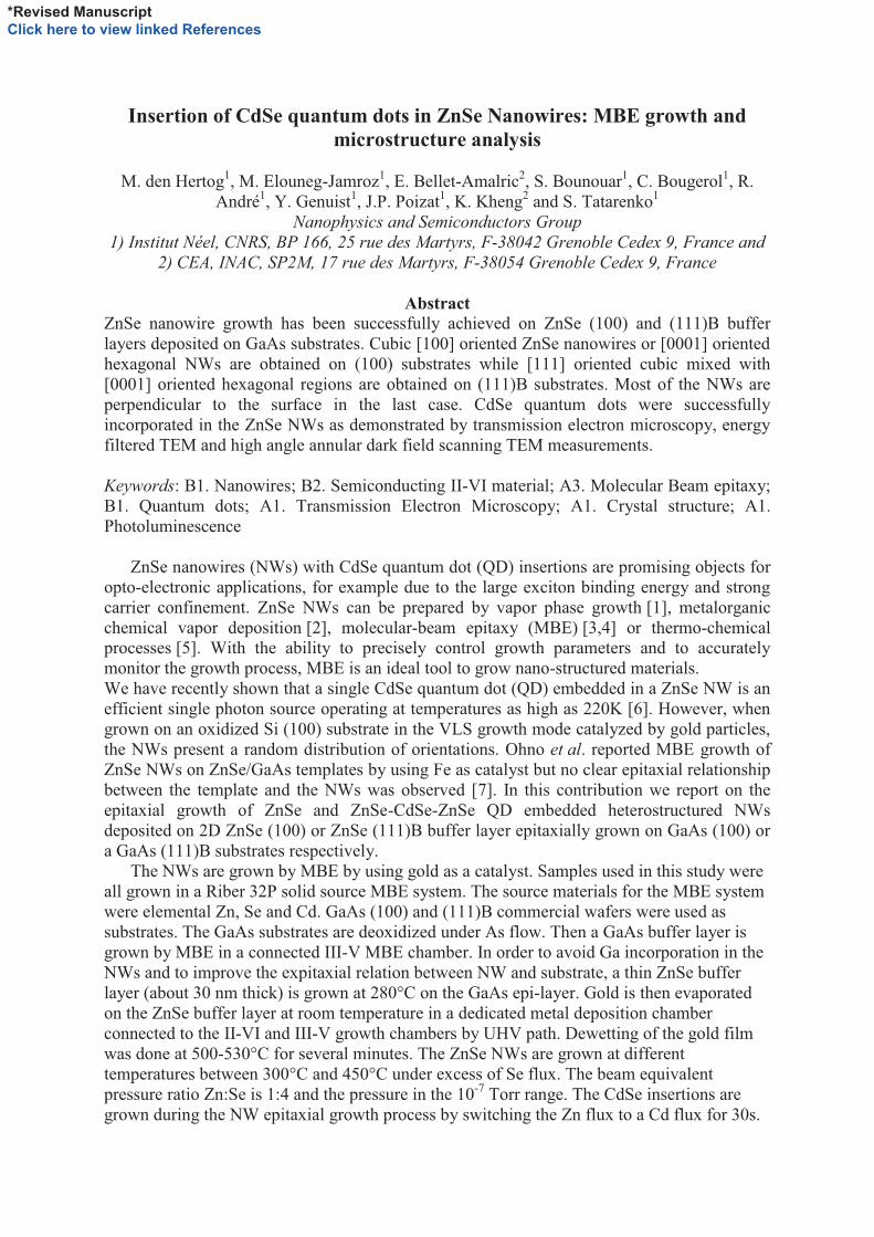
oriented cubic and [0001] oriented hexagonal regions (Fig. 3). Independent of the substrate,
the NWs have diameters around 10 nm, close to the bulk CdSe exciton Bohr diameter (11nm).
Fig 1 SEM images of 30nm ZnSe buffer layer with a 0.1 nm thick Au layer heated (A) at 530°C and (B) at
500°C
Fig. 2. SEM images (A,B) and TEM image (C) of cubic ZnSe NWs grown on a ZnSe/GaAs (100) buffer layers.
A B
500 nm 200 nm
A B C
200 nm 200 nm
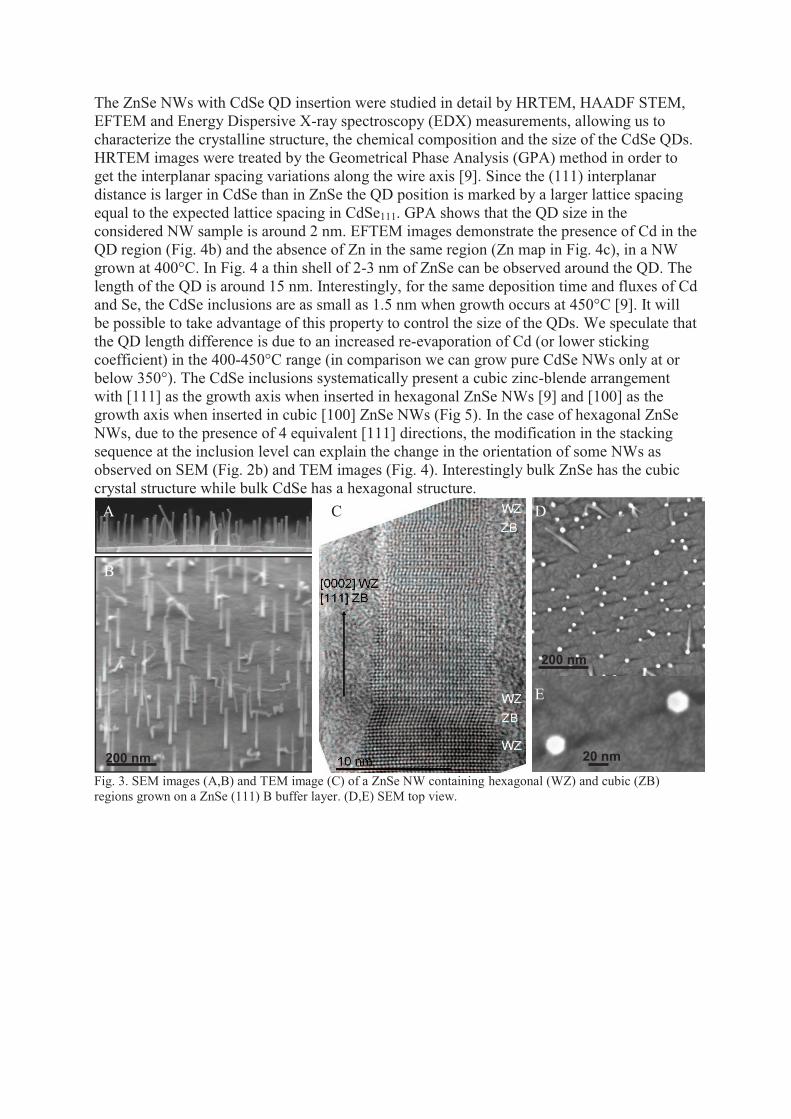
The ZnSe NWs with CdSe QD insertion were studied in detail by HRTEM, HAADF STEM,
EFTEM and Energy Dispersive X-ray spectroscopy (EDX) measurements, allowing us to
characterize the crystalline structure, the chemical composition and the size of the CdSe QDs.
HRTEM images were treated by the Geometrical Phase Analysis (GPA) method in order to
get the interplanar spacing variations along the wire axis [9]. Since the (111) interplanar
distance is larger in CdSe than in ZnSe the QD position is marked by a larger lattice spacing
equal to the expected lattice spacing in CdSe111. GPA shows that the QD size in the
considered NW sample is around 2 nm. EFTEM images demonstrate the presence of Cd in the
QD region (Fig. 4b) and the absence of Zn in the same region (Zn map in Fig. 4c), in a NW
grown at 400°C. In Fig. 4 a thin shell of 2-3 nm of ZnSe can be observed around the QD. The
length of the QD is around 15 nm. Interestingly, for the same deposition time and fluxes of Cd
and Se, the CdSe inclusions are as small as 1.5 nm when growth occurs at 450°C [9]. It will
be possible to take advantage of this property to control the size of the QDs. We speculate that
the QD length difference is due to an increased re-evaporation of Cd (or lower sticking
coefficient) in the 400-450°C range (in comparison we can grow pure CdSe NWs only at or
below 350°). The CdSe inclusions systematically present a cubic zinc-blende arrangement
with [111] as the growth axis when inserted in hexagonal ZnSe NWs [9] and [100] as the
growth axis when inserted in cubic [100] ZnSe NWs (Fig 5). In the case of hexagonal ZnSe
NWs, due to the presence of 4 equivalent [111] directions, the modification in the stacking
sequence at the inclusion level can explain the change in the orientation of some NWs as
observed on SEM (Fig. 2b) and TEM images (Fig. 4). Interestingly bulk ZnSe has the cubic
crystal structure while bulk CdSe has a hexagonal structure.
Fig. 3. SEM images (A,B) and TEM image (C) of a ZnSe NW containing hexagonal (WZ) and cubic (ZB)
regions grown on a ZnSe (111) B buffer layer. (D,E) SEM top view.
A
B
C D
E
200 nm
200 nm
20 nm
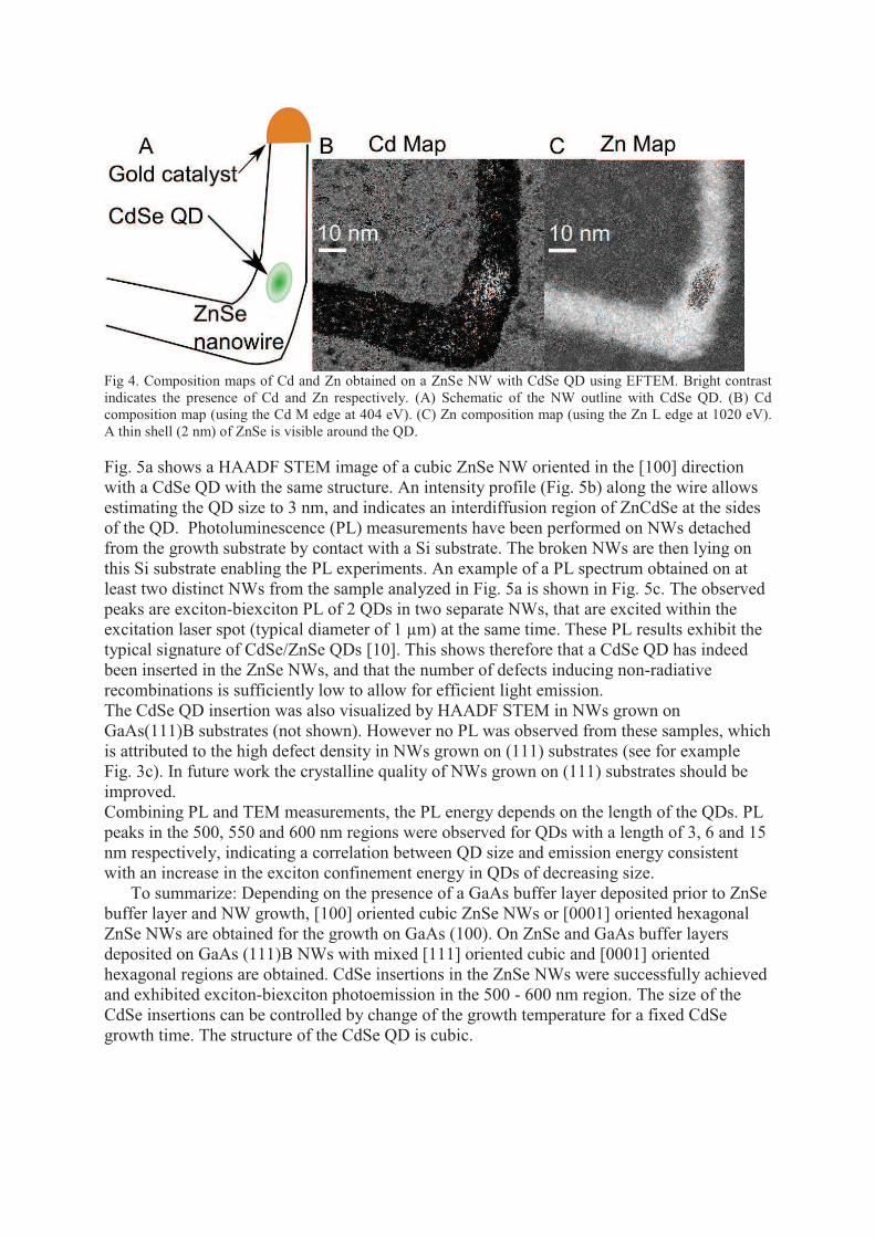
Fig 4. Composition maps of Cd and Zn obtained on a ZnSe NW with CdSe QD using EFTEM. Bright contrast
indicates the presence of Cd and Zn respectively. (A) Schematic of the NW outline with CdSe QD. (B) Cd
composition map (using the Cd M edge at 404 eV). (C) Zn composition map (using the Zn L edge at 1020 eV).
A thin shell (2 nm) of ZnSe is visible around the QD.
Fig. 5a shows a HAADF STEM image of a cubic ZnSe NW oriented in the [100] direction
with a CdSe QD with the same structure. An intensity profile (Fig. 5b) along the wire allows
estimating the QD size to 3 nm, and indicates an interdiffusion region of ZnCdSe at the sides
of the QD. Photoluminescence (PL) measurements have been performed on NWs detached
from the growth substrate by contact with a Si substrate. The broken NWs are then lying on
this Si substrate enabling the PL experiments. An example of a PL spectrum obtained on at
least two distinct NWs from the sample analyzed in Fig. 5a is shown in Fig. 5c. The observed
peaks are exciton-biexciton PL of 2 QDs in two separate NWs, that are excited within the
excitation laser spot (typical diameter of 1 µm) at the same time. These PL results exhibit the
typical signature of CdSe/ZnSe QDs [10]. This shows therefore that a CdSe QD has indeed
been inserted in the ZnSe NWs, and that the number of defects inducing non-radiative
recombinations is sufficiently low to allow for efficient light emission.
The CdSe QD insertion was also visualized by HAADF STEM in NWs grown on
GaAs(111)B substrates (not shown). However no PL was observed from these samples, which
is attributed to the high defect density in NWs grown on (111) substrates (see for example
Fig. 3c). In future work the crystalline quality of NWs grown on (111) substrates should be
improved.
Combining PL and TEM measurements, the PL energy depends on the length of the QDs. PL
peaks in the 500, 550 and 600 nm regions were observed for QDs with a length of 3, 6 and 15
nm respectively, indicating a correlation between QD size and emission energy consistent
with an increase in the exciton confinement energy in QDs of decreasing size.
To summarize: Depending on the presence of a GaAs buffer layer deposited prior to ZnSe
buffer layer and NW growth, [100] oriented cubic ZnSe NWs or [0001] oriented hexagonal
ZnSe NWs are obtained for the growth on GaAs (100). On ZnSe and GaAs buffer layers
deposited on GaAs (111)B NWs with mixed [111] oriented cubic and [0001] oriented
hexagonal regions are obtained. CdSe insertions in the ZnSe NWs were successfully achieved
and exhibited exciton-biexciton photoemission in the 500 - 600 nm region. The size of the
CdSe insertions can be controlled by change of the growth temperature for a fixed CdSe
growth time. The structure of the CdSe QD is cubic.
Fig. 5. (A) HAADF STEM image of a cubic NW oriented in the [100] direction with a CdSe QD (brighter
contrast) with the same crystalline phase and (B) Intensity profile along the NW. (C) PL spectrum of at least two
NWs from the same sample at an excitation wavelength of 405 nm at 4K. The two peaks labeled X and XX
correspond to an individual QD in a NW, and the peaks labeled X(2) and XX(2) correspond to another QD in
another NW.
Acknowledgements: This work is supported by French National Agency (ANR) through
Nanoscience and Nanotechnology Program (Project BONAFO n°ANR-08-NANO-031-01).
M E-J acknowledges financial support of the “Nanosciences aux Limites de
la Nanoélectronique” Foundation.
[1] B. Xiang, H.Z. Zhang, G.H. Li, F.H. Yang, F.H. Su, R.M. Wang, J. Xu, G.W. Lu, X.C. Sun, Q. Zhao and
D.P. Yu, Appl. Phys. Lett. 82 (2003) 3330.
[2] X.T. Zhang, K.M. Ip, Z. Liu, Y.P. Leung, Q. Li and S.K. Hark, Appl. Phys. Lett. 84 (2004) 2641.
[3] A. Colli, S. Hofmann, A.C. Ferrari, C. Ducati, F. Martelli, S. Rubini, S. Cabrini, A. Franciosi and J.
Robertson, Appl. Phys. Lett. 86 (2005) 153103.
[4] Y.F. Chan, X.F. Duan, S.K. Chan, I.K. Sou, X.X. Zhang and N. Wang, Appl. Phys. Lett. 83 (2005) 2665.
[5] Y.C. Zhu and Y. Bando, Chem. Phys. Lett. 377 (2003) 367.
[6] A. Tribu, G. Sallen, T. Aichele, R André, J.-Ph. Poizat, C. Bougerol, S. Tatarenko, and K. Kheng, Nano Lett. 8 (2008) 4326.
[7] Y. Ohno, T. Shirahama, S. Takeda, A. Ishizumi and Y. Kanemitsu, Appl. Phys. Lett. 87 (2005) 043105.
[8] S.K. Chan,S.K. Lok, G. Wang,Y. Cai, Y.J. Wang, N. Wang and I.K. Sou, Appl. Phys. Lett. 92 (2008)
183102.
[9] E. Bellet-Amalric, M. Elouneg-Jamroz,, C. Bougerol, M. Den Hertog, Y. Genuist, S. Bounouar, J.P. Poizat,
K. Kheng, R. André and S. Tatarenko Physica Statu Solidi C 7 (2010) 1527.
[10] G. Sallen, A. Tribu, R. André, L. Besombes, C. Bougerol, S. Tatarenko, K. Kheng and J.P. Poizat, Phys.
Rev. B 80 (2009) 085310.
A C
B