Embed Size (px)
Citation preview

Philips J. Res. 49 (1995) 279-292
InP-BASED INTEGRATED OPTICAL COMPONENTS
by RAYMOND VAN ROIJEN and BART H. VERBEEKPhilips Optoelectronics Centre, Prof Holstlaan 4, 5656 AA Eindhoven, The Netherlands
AbstractThe possibilities of fabricating integrated optical components on an lnPsubstrate are demonstrated by a number of devices that have beenmade in recent years. These components can have a major impact onevolving communication networks by facilitating new techniques forincreasing capacity such as wavelength division multiplexing and solitontransmission.Keywords: lnP, optoelectronics, integrated optics, wavelength division
multiplexing, soliton transmission.
1. Introduetion
The replacement of electrical communication networks by fibre opticalsystems is driven by the low loss and the extremely high bandwidth of glassfibre compared to twisted pair or coaxial copper cables. First the long-distance, high-capacity connections of the telephone system have beenreplaced by fibre, but currently the trend is to bring optical signals closerand closer to the user, eventually leading to fibre-to-the-home (FTTH). Thisis made possible by the application of InP-based semiconductor lasers andother components with their high performance/eest ratio. In this paper wewill discuss integrated optical components, that will help to realize opticalfunctions for an increase in the capacity and the flexibility of future networks.
Use of integrated optics implies that functions have to be performed in theoptical domain. Current and evolving network structures require an increasingnumber of optical functions. The demand for higher capacity and moreflexibility can be met by applying, for instance, higher bitrates through timedivision multiplexing and wavelength division multiplexing (WDM) tech-niques. In some cases the choice for integrated optical solutions is obvious
Philip. Journalof Research Vol.49 No.3 1995 279

R. van Roijen and B.H. Verbeek
or mandatory, in others optical functions can, at present, better be performedusing discrete components.
Depending on the complexity of network architecture the optical functionsthat need to be incorporated are: transmission and modulation of laser light atvarious bitrates, optical amplification, optical routing and switching, wave-length division multiplexing and demultiplexing, wavelength conversion andtime division (de)multiplexing.The Philips Optoelectronics Centre (pOC) is a manufacturer of high perfor-
mance semiconductor lasers, optical amplifiers and photodetectors. Thedemand for new functions and ongoing cost reduction requires integrationof these components. The combination oftechnological capabilities and mod-elling tools allows us to fabricate integrated optical devices at the forefront ofcurrent integration technology.
We will discuss a number of these InP-based integrated optical devices: acombination of an optical switch and amplifier, a tunable laser with inte-grated monitor, a tunable optical filter and amplifier, a wavelength demulti-plexer and a soliton source.
2. InP-based integrated optical devices
2.1. Optical switch with amplifier
An optical switch matrix is used for routing of signals, i.e. information isrouted from one fibre link to another, much like a conventional telephone con-nection. This will facilitate efficient use of connections and rerouting of signalsin the case of, for instance, a cable break, and is essential if networks are builtcompletely based on optical transmission.
Optical amplifiers can be used to boost signals for distribution and to com-pensate for fibre loss after transmission. Semiconductor laser amplifiers arevery attractive as part of integrated optics on InP because the light intensityloss due to optical couplers, switches etc. can conveniently be compensated.We have demonstrated the feasibility of employing optical amplifiers in this
way by monolithically integrating an optical switch and an amplifier [1]. Theswitch was a 2 x 1 type, enabling light from either oftwo inputs to go into oneoutput or vice versa. In Fig. 1 a schematic diagram of the switch is shown. Itconsists of two crossing, single-mode waveguides with a crossover region of aspecific length. Using the beam propagation method, the length of the cross-over region is determined. The optimum length for crossing was found to be70 J.Lm. At this length light predominantly crosses from one waveguide to theother side (Fig. 1, upper part). Another, simpler way to derive the required
280 PhlUps JournDl of Research Vol.49 No.3 1995

InP-based integrated optical components
DIndex change
Fig. 1. Schematic diagram of the operation of the optical switch. Without current injection lightpasses from the input port A to the output port D (top figure). If current is injected in the lowerhalf of the crossover region (lower figure) the index of refraction is lowered and light will be con-
. fined to the upper part and go from port B to D.
length is by calculating the effective refractive index of the fundamental andfirst-order modes. The crossing can then be viewed as constructive inter-ference of the two modes excited by the incoming beam into the outgoingwaveguide.By injecting current into one half of the crossover region the refractive index
of the material is lowered by an amount equal to the effective index differencebetween the waveguide and the surrounding material. Now the light is con-fined, passing through the remaining high-index part to the waveguide atthe same side (Fig. 1, lower part). This device was realized using the ridgewaveguide technology. The switching part of the chip, with the crossing wave-guide, can be seen in Fig. 2. The switch has a crosstalk value of ~ 12dB and a,chip loss of 2-4dB. In practice, however, one would probably want to use alarger switch matrix (for instance 4 x 4), and, in addition, we have to accountfor fibre chip coupling loss, typically 3 dB per coupling. Therefore, the switchwas integrated with an optical amplifier with high gain (20dB). As a result theamplifier/switch chip shows a net gain of 10dB even after switching andcoupling loss, with a saturation level of 3 dBm (Fig. 3). This means thatwith identical technology the device has the potentialof a lossless 4 x 4
Philips Journal of Research Vol.49 No.3 1995 281

R. van Roijen and B.H. Verbeek
Fig. 2. SEM micrograph of the two crossing waveguides of the optical switch chip. The metalextending over the ridges is used for the current injection in the switch.
switch. This work was supported by European RACE project 1064 (MIOCA)on monolithic integration.
2.2. Tunable laser with integrated monitor
In the same RACE project another demonstration of integration was thedistributed Bragg reflector (DBR) laser with monitor diode. Packaged, com-mercially available lasers have a monitor diode inside the package, thatmeasures the light intensity to stabilize output power. Because a standardlaser without coatings will emit equal power from both ends, the monitorcan be conveniently located behind the laser. The DBR laser is a specialcase because the integrated Bragg reflector inside the laser cavity consists ofa reflecting grating which is wavelength-selective. The grating enhances thewavelength stability of the DBR laser compared to ordinary semiconductorlasers. However, since the grating reflects most of the light, less light isavailable for the monitor. Light from the rear facet may no longer beproportional to the light emitted at the front, which is coupled into thefibre. For this reason it is desirable to measure the front facet power
282 Philips Journalof Research Vol. 49 No.3 1995

InP-based integrated optical components
12108.........
CC"0 6---c:: 4'(ijCl.... 2Q)..c 0;:0- -2....Q)..c -4u::
-6 :~D-8
o AD, OmA• AD,100mA .v BD, 0 mA'f' BD,100mA
_10L_ __ _L ~ __ _L ~~_J
1500 1520 1540 1560 1580 1600Wavelength (nm)
Fig. 3. Fibre-to-fibre gain of the paths A to D and B to D for the.situation with and without injec-tion current in the crossover region. The current in the amplifier section is 200mA. The switchingbehaviour is clearly demonstrated. Note also the high fibre-to-fibre gain due to the amplifier.
directly. We have accomplished this by using part of the laser structure as amonitor diode.
One of the properties of the laser diode structure is that while under normaloperation current is injected, which is converted to light, it is also possible tooperate the diode in reverse to form a photodiode. We have succeeded in rig-orously separating the laser and the monitor part of the device by etching adeep channel all the way through the active layer, as shown in Fig. 4. Theschematic diagram shows the DBR grating for wavelength selection, thegain section for laser operation and the monitor, separated from the gainsection by the etched channel. This channel serves two purposes: first oneside acts as a front mirror for the DBR laser, so the monitor section doesnot interfere with the laser section. This implies, amongst other things, thatthe etched sidewall has to be vertical. Laser operation as a function of wave-length tuning current clearly showed that this was indeed the case. Second, thechannel creates high electrical isolation (> 1Mn) between laser and monitor,so we can reversely bias the monitor and accurately determine monitorcurrent. In Fig. 5 the monitor current and the signalof an external, fibrecoupled detector are compared. The monitor current is found to be anaccurate measure of the laser output, independent of the laser wavelength.
283Philips Journalof Research Vol.49 No.3 1995

R. van Roijen and B.H. Verbeek
gain section\ monitor diodegrating section 1\~¥::::VV_~_~'/ ()
\ ,
etched channel
lightoutput
Fig, 4. Diagram ofthe tunable DBR laser with integrated monitor and SEM picture of the etchedchannel between the laser and the monitor section, The channel is less than 3p,m wide, To max-imize the coupling of light to the monitor and the fibre the etched sidewall has to be perpendicular
to the waveguide.
2.3. Tunable optical filter and amplifier chip
Currently we are fabricating a chip meant for the receiver side of a WDMsystem. It is a tunable filter, amplifier and detector, consisting of a three-section distributed feedback (DFB) structure, a passive waveguide and adetector section. The three-section DFB structure is operated just below itsthreshold current, so that light coming in at its filter wavelength will bestrongly amplified. In this way a single wavelength channel is selected, andthe optical amplification strongly increases the ability to handle low-power
284 Philip, Journalof Research Vol. 49 NO.3 1995

lnP-based integrated optical components
Monitor current (!lA)300 r--------------------------,
Philip. Joumal of Research Vol.49 No.3 1995 285
oOu put power (mW)
1.0
200
100
.... 0.5
o 20 40 60 80 100Injection current (mA)
Fig. 5. Monitor current (upper half) and externally determined output power (lower half) as afunction of injection current for the DBR laser with integrated monitor.
signals. The wavelength can be tuned by varying the current in the threesections. We have successfully tested a DFB structure as a filter and amplifier[2]. The gain bandwidth can be varied through the injection current, and canbe as small as 2.5 GHz. The 18dB fibre-to-fibre gain at low power increases thenumber of potential subscribers by a factor of ten or more if this device isincluded in the receiver of a distributed network. This has a major impacton the technical and economic viability of such networks.
Recently the first integrated filter, amplifier and detector chips have beentested by measuring the current in the detector section as a function of thewavelength and the power of the incoming optical signal from a tunablelaser. In Fig. 6 it can be seen that the gain of the DFB section at the selectedwavelength is approximately 15dB. Therefore signals can be detected at inputpowers well below -30dBm.
2.4. Wavelength demultiplexer chip
The capacity of optical fibres can be increased using independent opticalcarriers with different wavelengths in high density (HD) WDM system appli-cations. Essential components are optical wavelength multiplexers anddemultiplexers. A multiplexer combines the different wavelengths fromseveral sources into a single fibre with minimum opticallosses and the demulti-plexer has the opposite function.

R. van Roijen and B.H. Verbeek
0.05
0.04 f-
~ 0.03~
I-
~QJI\.<I\.< 0.02 f-f;3
Detector responseDFB current injection 70 mASpontaneous emission0.1627 mA
~• I, .• I, .; ~• I~ ,, X, I, ,, I, ,, I, ,X + !,. " + ~, + ' tx r . +.
I • + ;~X X .. AAA. ' x.. ..' .+.+.+ti Ai..L~~:ft> A CCC .\t.j.. X'>lX
O00 XxXXl:(?$,,,,dA-;:;Cj CnH;!;:!:"'Y.,.l:<l:<l:<X"vvv". ~~~~'~~~~~~~~~~~~1552.8 1553.0 1553.2
0.01 f-
C-C -40 dBm
A--A -36 dBm
+._-+ -33 dBm
X--'X -30 dBm
Wavelength (nm)
Fig. 6. Current in the detector section as a function of input wavelength at input powers between-30 and -40dBm. The injection current in the filter/amplifier section is 70mA, the DC current
due to spontaneous emission is 0.16mA.
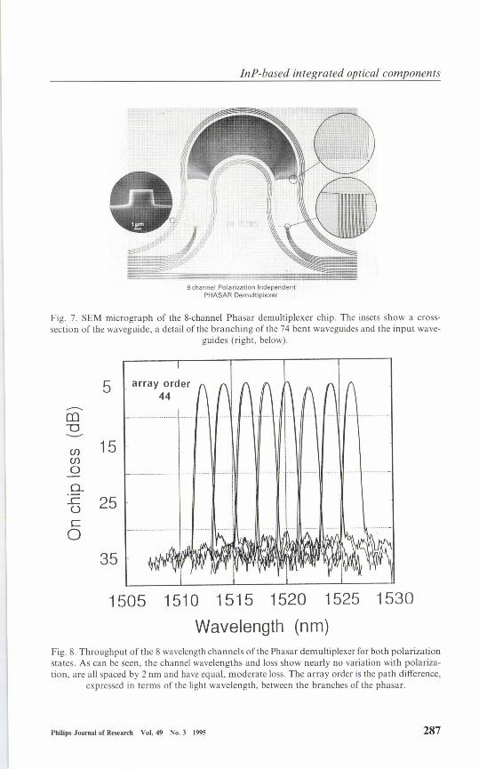
Since the polarization state of the different optical channels is undeterminedand slowly fluctuating, it is important to have available a polarization-independent demultiplexer with low insertion loss. At poe, we have recentlyachieved this integrated optical demultiplexer using polarization-independent(i.e. non-birefringent) optical waveguides in an array of bent waveguides,in which different optical pathlengths are employed for dispersion similarto the well known prism [3]. This concept has been developed by the DelftUniversity of Technology Integrated Optics Group and is now called thephasar. It consists of 74 bent waveguides with radii varying between 500 f.Lmand 700 f.Lm that have focusing properties. Figure 7 shows the layout ofthe phasar designed for 8 channels with a 2 nm channel spacing in the1525nm window. Since the design is symmetrical, light input and output wave-guides have been used to increase wavelength tolerance. This symmetryimplies multiplexing as well as demultiplexing, but the device can also be
286 Philips Journal of Research VoI.49 No.3 1995
InP-based integrated optical components
8 channel Polarization IndependentPHASAR Demultiplexer
Fig. 7. SEM micrograph of the 8-channel Phasar demultiplexer chip. The insets show a cross-section of the waveguide, a detail of the branching of the 74 bent waveguides and the input wave-
guides (right, below).
5 array order44
Cf)Cf)
oo,...cUco
15
25 .
35 -
1505 1510 151 5 1520 1525
Wavelength (nm)1530
Fig. 8. Throughput ofthe 8 wavelength channels ofthe Phasar demultiplexer for both polarizationstates. As can be seen, the channel wavelengths and loss show nearly no variation with polariza-tion, are all spaced by 2 nm and have equal, moderate loss. The array order is the path difference,
expressed in terms of the light wavelength, between the branches of the phasar.
Philips Journalof Research Vol. 49 No.3 1995 287
R. van Roijen and B.H. Verbeek
absorber section
absorber... ....AllAlight pulse
288 PhiUps Journal of Research Vol. 49 No.3 1995
....A
Fig. 9. Schematic diagram of a CPM laser and pulse shaping by the saturable absorber section. Thepulse shaping in the absorber occurs as follows: the first part of two pulses arriving simultaneouslyfrom two sides of the absorber will be attenuated (second picture), but as the intensity increases theabsorber is saturated, and the peaks of the pulses pass the absorber with little or no loss, resulting
in shorter pulses (third picture).
used as a wavelength filter by connecting one input to one output waveguide.Figure 8 shows the performance of the passive integrated optical chip. On-chiplosses are 4-5 dB, crosstalk is better than 25 dB, the channel bandwidth is0.9 nm and the small size is 2.6 x 2.3 mm". This chip has very small fibrechip coupling losses ( < 0.5 dB) due to the specially designed waveguide geo-metry (see Fig. 7 inset) which allows a large, symmetrical spot. This workwas partly supported by European RACE project R2070 (MUNDI).
2.5. Passive mode-locked source for long-distance transmission
Direct electrical modulation of lasers is presently used up to 2.5 Gb/s, butfundamental difficulties concerning laser and fibre properties arise at higher
lnP-based integrated optical components
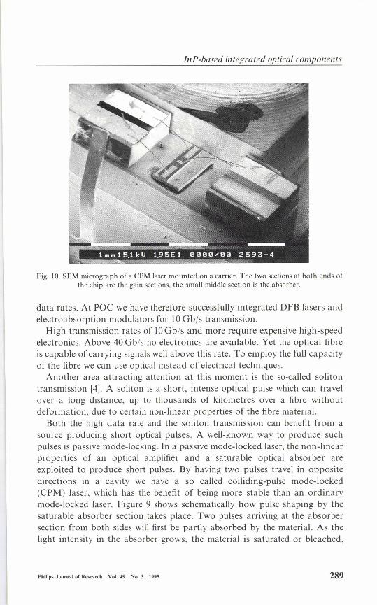
Fig. ID. SEM micrograph of a CPM laser mounted on a carrier. The two sections at both ends ofthe chip are the gain sections, the small middle section is the absorber.
data rates. At POC we have therefore successfully integrated DFB lasers andelectroabsorption modulators for 10Gb/s transmission.
High transmission rates of 10Gb/s and more require expensive high-speedelectronics. Above 40 Gb/s no electronics are available. Yet the optical fibreis capable of carrying signals well above this rate. To employ the full capacityof the fibre we can use optical instead of electrical techniques.
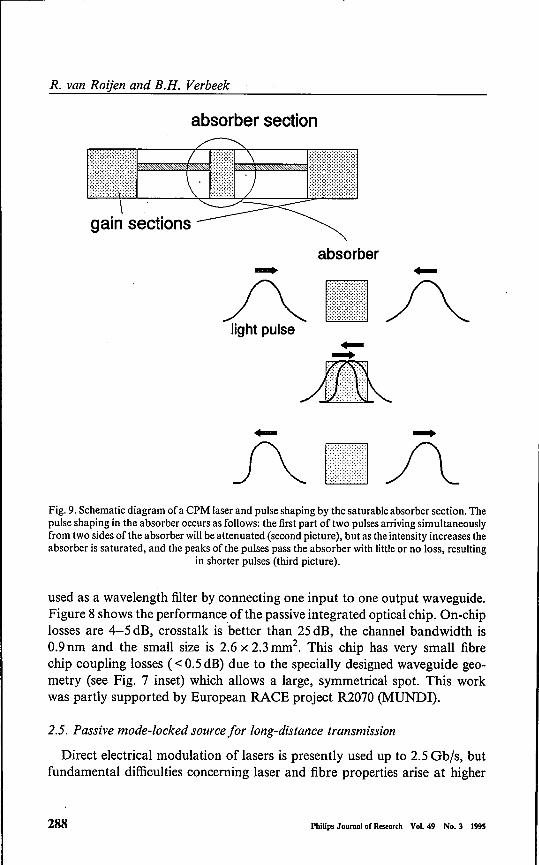
Another area attracting attention at this moment is the so-called soli tontransmission [4]. A soliton is a short, intense optical pulse which can travelover a long distance, up to thousands of kilometres over a fibre withoutdeformation, due to certain non-linear properties of the fibre material.
Both the high data rate and the soli ton transmission can benefit from asource producing short optical pulses. A well-known way to produce suchpulses is passive mode-locking. In a passive mode-locked laser, the non-linearproperties of an optical amplifier and a saturable optical absorber areexploited to produce short pulses. By having two pulses travel in oppositedirections in a cavity we have a so called colliding-pulse mode-locked(CPM) laser, which has the benefit of being more stable than an ordinarymode-locked laser. Figure 9 shows schematically how pulse shaping by thesaturable absorber section takes place. Two pulses arriving at the absorbersection from both sides will first be partly absorbed by the material. As thelight intensity in the absorber grows, the material is saturated or bleached,
Philips Journalof Research Vol. 49 No.3 1995 289
R. van Roijen and B.H. Verbeek
Secant hyperbolic fit
0.9
Pulse width (FWHM): 580 fs
c::oNo.8êogO.7::::ItU~0.6ëiic:~0.5.£o'§0.4§_êO.3'Cc::80.2al(/)
0.1
-1 -0.5 °Delay (ps)0.5
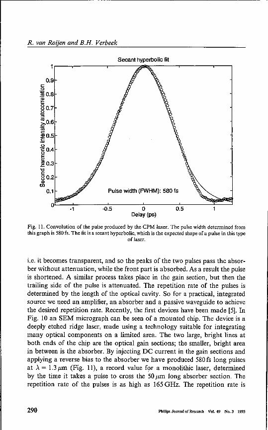
Fig. 11. Convolution of the pulse produced by the CPM laser. The pulse width determined fromthis graph is 580 fs. The fit is a secant hyperbolic, which is the expected shape of a pulse in this type
of laser.
i.e. it becomes transparent, and so the peaks of the two pulses pass the absor-ber without attenuation, while the front part is absorbed. As a result the pulseis shortened. A similar process takes place in the gain section, but then thetrailing side of the pulse is attenuated. The repetition rate of the pulses isdetermined by the length of the optical cavity. So for a practical, integratedsource we need an amplifier, an absorber and a passive waveguide to achievethe desired repetition rate. Recently, the first devices have been made [5]. InFig. 10 an SEM micrograph can be seen of a mounted chip. The device is adeeply etched ridge laser, made using a technology suitable for integratingmany optical components on a limited area. The two large, bright lines atboth ends of the chip are the optical gain sections; the smaller, bright areain between is the absorber. By injecting DC current in the gain sections andapplying a reverse bias to the absorber we have produced 580fs long pulsesat À = 1.3/Lm (Fig. 11), a record value for a monolithic laser, determinedby the time it takes a pulse to cross the 50/Lm long absorber section. Therepetition rate of the pulses is as high as 165GHz. The repetition rate is
290 Phllips Journalof Research Vol.49 No.3 1995

lnP-based integrated optical components
determined simply in the design of the cavity, through the roundtrip time of apulse.
3. Integrated optics on InP substrates versus silicon integrated circuits
Integrated optic components, sometimes called photonic integrated circuits(PICs), are often compared to the well-known electronic silicon ICs. The sameadvantages of compactness, functionality and reliability apply, so one wouldexpect a similar explosive development in optical ICs. In spite of impressivedemonstrations in research, integrated optics has not yet massively reachedthe production stage. The reason for this can be found partly by consideringthe immaturity of the field, but there are also some more fundamental differ-ences which in the foreseeable future will cause the development to differ fromthe silicon IC. As can already be observed in the previous paragraphs, thereexist a wealth of solutions for many integration challenges on InP sub-strates. In the end, this will enable us to fabricate integrated chips withmany functions. Although interesting from a research point of view, thisdoes not help to establish generally accepted designs and processes. Conse-quently production will only take off once a consensus has been reached.
Other factors that are not likely to change soon are the larger dimension ofoptical ICs compared with silicon ICs. This is fundamentally due to the largephoton wavelength and the difficulty to manipulate light compared to elec-trons. Finally, as is also apparent from the discussion above, the operationsperformed on optical signals are handled by a number of very differentdevices, whereas an electronic IC usually consists of a large number of onlyone type of transistor and a few other very simple elements [6].This work was supported in part by RACE project 2073 (OMAN) on inte-
grated optics for the access network.
REFERENCES[I] R. van Roijen, J.M.M. van der Heijden, L.F. Tiemeijer, P.J.A. Thijs, T. van Dongen, J.J.M.
Binsma and B.H. Verbeek, IEEE Photonics Techno!. Lett., 5, 529 (1993).[2] L.F. Tiemeijer, P.J.A. Thijs, J.J.M. Binsma, R. van Roijen, T. van Dongen and L.J.G. van der
Helm, IEEE Phot. Techno!. Lett., 6, 179 (1994).[3] B.H. Verbeek, A.A.M. Staring, E.J. Jansen, R. van Roijen, J.J.M. Binsma, T. van Dongen,
M.R. Amersfoort, C. van Dam and M.K. Smit, Proc. OFC '94, San Jose, USA, Postdeadlinepaper PDP13, p. 63, 1994.
[4] C.T.H.F. Liedenbaum, JJ.E. Reid, L.F.Tiemeijer, A.J. Boot, P.1.Kuindersma, I.Gabitov andA. Mattheus, accepted for presentation at ECOC '94, Florence.
[5] R.G.M.P. Koumans, R. van Roijen, M.B. van der Mark, E.J. Jansen, J.J.M. Binsma, P.J.A.Thijs, T. van Dongen, L.F. Tiemeijer, C.T.H.F. Liedenbaum and J.J.E. Reid, Optical FibreConference, San Diego, CA, 1995, paper TuB.
[6] M. Erman, Proc. European Conf. on Integrated Optics '93, Neuchatel, Switzerland, 1993.
Phllips Journal of Research Vol. 49 No. 3 1995 291

R. van Roijen and B.H. Verbeek
Authors
Raymond van Roijen received his MS degree in physics at the Universityof Leiden in 1984 and the doctorate in physics at the University ofAmsterdam in 1989. Since 1989 he has been working at the PhilipsResearch Laboratory in Eindhoven on the application of dry etchingand the fabrication of integrated optical devices on III-V materials.
Bart H. Verbeek received the MS degree in 1975 and the PhD degree (cum laude) in 1979. Hejoined Philips Research Laboratories in Eindhoven, The Netherlands, where he was engaged inresearch on the electronic structure of metal-semiconductor compounds studied by UV andsynchrotron radiation and later with AlGaAs semiconductor lasers for CD applications, especi-ally on optical feedback effects. In 1986 he worked as a visiting research scientist at AT&T BellLaboratories, Murray Hill, Nl, on semiconductor lasers and integrated optics for telecommunica-tion applications. He returned to Philips Research in 1987, where his main areas of research in thePhilips Optoelectronics Centre are optoelectronic components and InP-based integrated optics forcommunication applications. He is also involved in European RACE projects. He is part-timeprofessor at the Technical University of Delft, giving lectures on optical fibre communicationtechnology, and heads the Integrated Optics Research Group. He is author and co-author ofover 70 scientific publications and conference contributions.
292 Philips Journalof Research Vol.49 No. 3 1995