Embed Size (px)
Citation preview
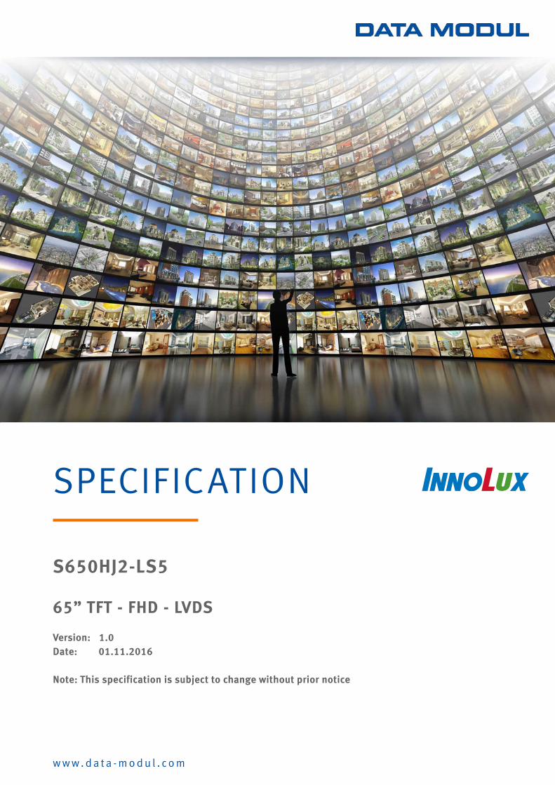
S650HJ2-LS5
65” TFT - FHD - LVDS
Version: 1.0Date: 01.11.2016
Note: This specification is subject to change without prior notice
SPECIFICATION
w w w . d a t a - m o d u l . c o m
PRODUCT SPECIFICATION
Version 1.0 1 Date : Nov. 01, 2016The copyright belongs to InnoLux. Any unauthorized use is prohibited
Revision : 21Customer : Foxconn
APPROVED BY SIGNATURE
Name / TitleNote
Please return 1 copy for your confirmation with your signature and comments.
Tentative Specification Preliminary Specification Approval Specification
MODEL NO.: S650HJ2
SUFFIX: LS5
Approved By Checked By Prepared By
Chao-Chun Chung Carlos Lee John.Hsieh
PRODUCT SPECIFICATION
Version 1.0 2 Date : Nov. 01, 2016The copyright belongs to InnoLux. Any unauthorized use is prohibited
CONTENTS
CONTENTS....................................................................................................................................................................................... 2
REVISION HISTORY....................................................................................................................................................................... 4
1. GENERAL DESCRIPTION..........................................................................................................................................................5
1.1 OVERVIEW......................................................................................................................................................................... 5
1.2 FEATURES..........................................................................................................................................................................5
1.3 GENERAL SPECIFICATIONS..........................................................................................................................................5
1.4 MECHANICAL SPECIFICATIONS...................................................................................................................................6
2. ABSOLUTE MAXIMUM RATINGS.............................................................................................................................................7
2.1 ABSOLUTE RATINGS OF ENVIRONMENT.................................................................................................................. 7
2.2 PACKAGE STORAGE....................................................................................................................................................... 8
2.3 ELECTRICAL ABSOLUTE RATINGS..............................................................................................................................8
2.3.1 TFT LCD MODULE.........................................................................................................................................................8
2.3.2 BACKLIGHT CONVERTER UNIT................................................................................................................................ 8
3. ELECTRICAL CHARACTERISTICS..........................................................................................................................................9
3.1 TFT LCD MODULE............................................................................................................................................................ 9
3.2 BACKLIGHT UNIT........................................................................................................................................................... 12
3.2.1 CONVERTER CHARACTERISTICS..........................................................................................................................12
3.2.2 CONVERTER INTERFACE CHARACTERISTICS.................................................................................................. 14
4. BLOCK DIAGRAM OF INTERFACE....................................................................................................................................... 16
4.1 TFT LCD MODULE.......................................................................................................................................................... 16
5 .INPUT TERMINAL PIN ASSIGNMENT...................................................................................................................................17
5.1 TFT LCD MODULE.......................................................................................................................................................... 17
5.2 BACKLIGHT UNIT........................................................................................................................................................... 20
5.3 CONVERTER UNIT......................................................................................................................................................... 21
5.4 LVDS INTERFACE...........................................................................................................................................................21
5.5 COLOR DATA INPUT ASSIGNMENT........................................................................................................................... 24
6. INTERFACE TIMING................................................................................................................................................................. 24
6.1 INPUT SIGNAL TIMING SPECIFICATIONS................................................................................................................ 25
6.1.1 Timing spec for Frame Rate = 50Hz.................................................................................................................. 25
6.1.2 Timing spec for Frame Rate = 60Hz.................................................................................................................. 26
PRODUCT SPECIFICATION
Version 1.0 3 Date : Nov. 01, 2016The copyright belongs to InnoLux. Any unauthorized use is prohibited
6.2 POWER ON/OFF SEQUENCE......................................................................................................................................26
7. OPTICAL CHARACTERISTICS............................................................................................................................................... 31
7.1 TEST CONDITIONS........................................................................................................................................................ 31
7.2 OPTICAL SPECIFICATIONS..........................................................................................................................................32
8. PRECAUTIONS..........................................................................................................................................................................36
8.1 ASSEMBLY AND HANDLING PRECAUTIONS...........................................................................................................36
8.2 SAFETY PRECAUTIONS............................................................................................................................................... 36
8.3 SAFETY STANDARDS....................................................................................................................................................36
9. DEFINITION OF LABELS......................................................................................................................................................... 38
9.1 MODULE LABEL..............................................................................................................................................................38
9.2 CARTON LABEL.............................................................................................................................................................. 39
10. PACKAGING.............................................................................................................................................................................40
10.1 PACKAGING SPECIFICATIONS.................................................................................................................................40
10.2 PACKAGING METHOD................................................................................................................................................ 40
10.3 UN-PACKAGING METHOD......................................................................................................................................... 41
11. MECHANICAL CHARACTERISTIC.......................................................................................................................................42
PRODUCT SPECIFICATION
Version 1.0 4 Date : Nov. 01, 2016The copyright belongs to InnoLux. Any unauthorized use is prohibited
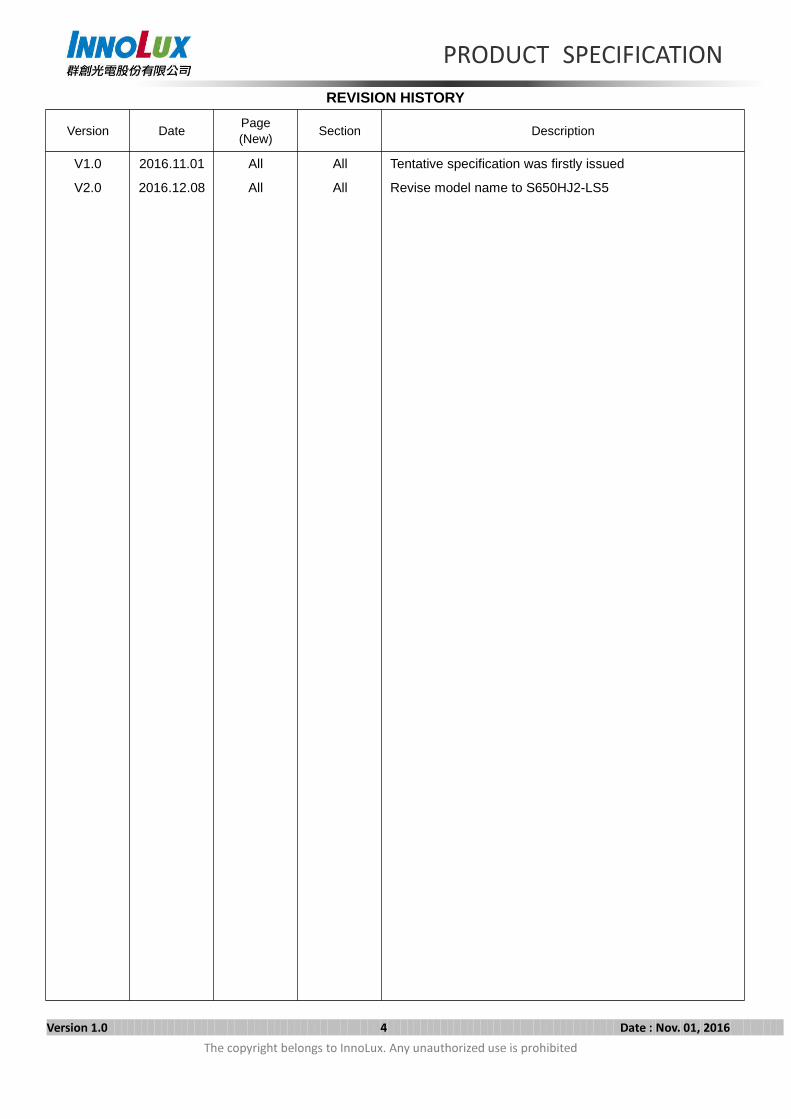
REVISION HISTORY
Version DatePage(New)
Section Description
V1.0
V2.0
2016.11.01
2016.12.08
All
All
All
All
Tentative specification was firstly issued
Revise model name to S650HJ2-LS5
PRODUCT SPECIFICATION
Version 1.0 5 Date : Nov. 01, 2016The copyright belongs to InnoLux. Any unauthorized use is prohibited
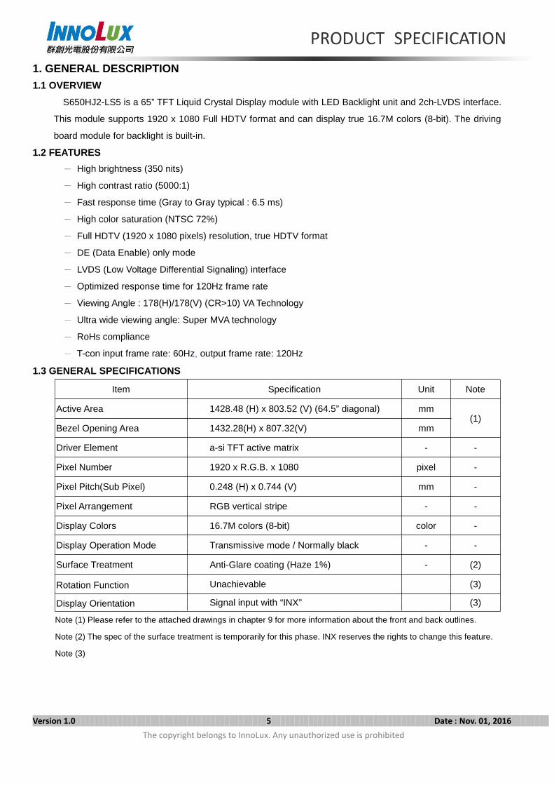
1. GENERAL DESCRIPTION1.1 OVERVIEW
S650HJ2-LS5 is a 65” TFT Liquid Crystal Display module with LED Backlight unit and 2ch-LVDS interface.
This module supports 1920 x 1080 Full HDTV format and can display true 16.7M colors (8-bit). The driving
board module for backlight is built-in.
1.2 FEATURES
- High brightness (350 nits)
- High contrast ratio (5000:1)
- Fast response time (Gray to Gray typical : 6.5 ms)
- High color saturation (NTSC 72%)
- Full HDTV (1920 x 1080 pixels) resolution, true HDTV format
- DE (Data Enable) only mode
- LVDS (Low Voltage Differential Signaling) interface
- Optimized response time for 120Hz frame rate
- Viewing Angle : 178(H)/178(V) (CR>10) VA Technology
- Ultra wide viewing angle: Super MVA technology
- RoHs compliance
- T-con input frame rate: 60Hz, output frame rate: 120Hz
1.3 GENERAL SPECIFICATIONS
Item Specification Unit Note
Active Area 1428.48 (H) x 803.52 (V) (64.5” diagonal) mm(1)
Bezel Opening Area 1432.28(H) x 807.32(V) mm
Driver Element a-si TFT active matrix - -
Pixel Number 1920 x R.G.B. x 1080 pixel -
Pixel Pitch(Sub Pixel) 0.248 (H) x 0.744 (V) mm -
Pixel Arrangement RGB vertical stripe - -
Display Colors 16.7M colors (8-bit) color -
Display Operation Mode Transmissive mode / Normally black - -
Surface Treatment Anti-Glare coating (Haze 1%) - (2)
Rotation Function Unachievable (3)
Display Orientation Signal input with “INX” (3)
Note (1) Please refer to the attached drawings in chapter 9 for more information about the front and back outlines.
Note (2) The spec of the surface treatment is temporarily for this phase. INX reserves the rights to change this feature.
Note (3)
PRODUCT SPECIFICATION
Version 1.0 6 Date : Nov. 01, 2016The copyright belongs to InnoLux. Any unauthorized use is prohibited
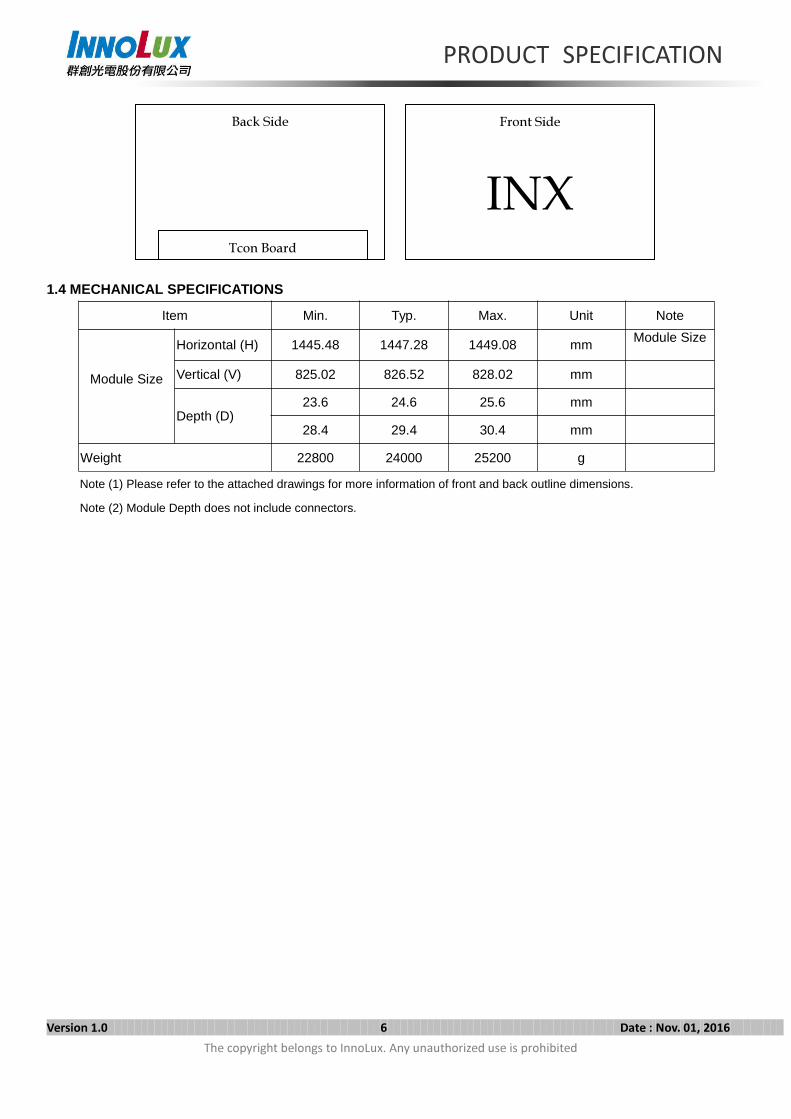
1.4 MECHANICAL SPECIFICATIONS
Item Min. Typ. Max. Unit Note
Module Size
Horizontal (H) 1445.48 1447.28 1449.08 mm Module Size
Vertical (V) 825.02 826.52 828.02 mm
Depth (D)23.6 24.6 25.6 mm
28.4 29.4 30.4 mm
Weight 22800 24000 25200 g
Note (1) Please refer to the attached drawings for more information of front and back outline dimensions.
Note (2) Module Depth does not include connectors.
Back Side
Tcon Board
Front Side
INX
PRODUCT SPECIFICATION
Version 1.0 7 Date : Nov. 01, 2016The copyright belongs to InnoLux. Any unauthorized use is prohibited
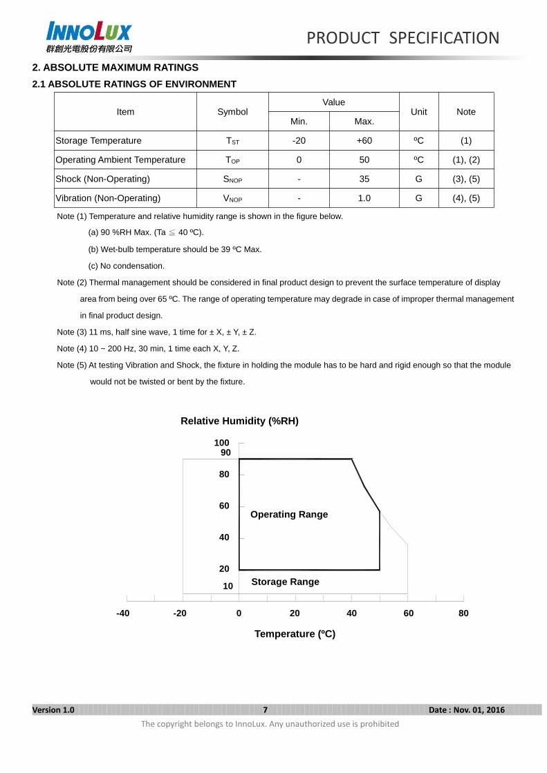
2. ABSOLUTE MAXIMUM RATINGS
2.1 ABSOLUTE RATINGS OF ENVIRONMENT
Item SymbolValue
Unit NoteMin. Max.
Storage Temperature TST -20 +60 ºC (1)
Operating Ambient Temperature TOP 0 50 ºC (1), (2)
Shock (Non-Operating) SNOP - 35 G (3), (5)
Vibration (Non-Operating) VNOP - 1.0 G (4), (5)
Note (1) Temperature and relative humidity range is shown in the figure below.
(a) 90 %RH Max. (Ta ≦ 40 ºC).
(b) Wet-bulb temperature should be 39 ºC Max.
(c) No condensation.
Note (2) Thermal management should be considered in final product design to prevent the surface temperature of display
area from being over 65 ºC. The range of operating temperature may degrade in case of improper thermal management
in final product design.
Note (3) 11 ms, half sine wave, 1 time for ± X, ± Y, ± Z.
Note (4) 10 ~ 200 Hz, 30 min, 1 time each X, Y, Z.
Note (5) At testing Vibration and Shock, the fixture in holding the module has to be hard and rigid enough so that the module
would not be twisted or bent by the fixture.
Relative Humidity (%RH)
Operating Range
Temperature (ºC)
100
8060-20 400 20-40
90
80
40
60
20
10 Storage Range
PRODUCT SPECIFICATION
Version 1.0 8 Date : Nov. 01, 2016The copyright belongs to InnoLux. Any unauthorized use is prohibited
2.2 PACKAGE STORAGE
When storing modules as spares for a long time, the following precaution is necessary.
(a) Do not leave the module in high temperature, and high humidity for a long time, It is highly recommended to
store the module with temperature from 0 to 35 at normal humidity without condensation.
(b) The module shall be stored in dark place. Do not store the TFT-LCD module in direct sunlight or fluorescent
light.
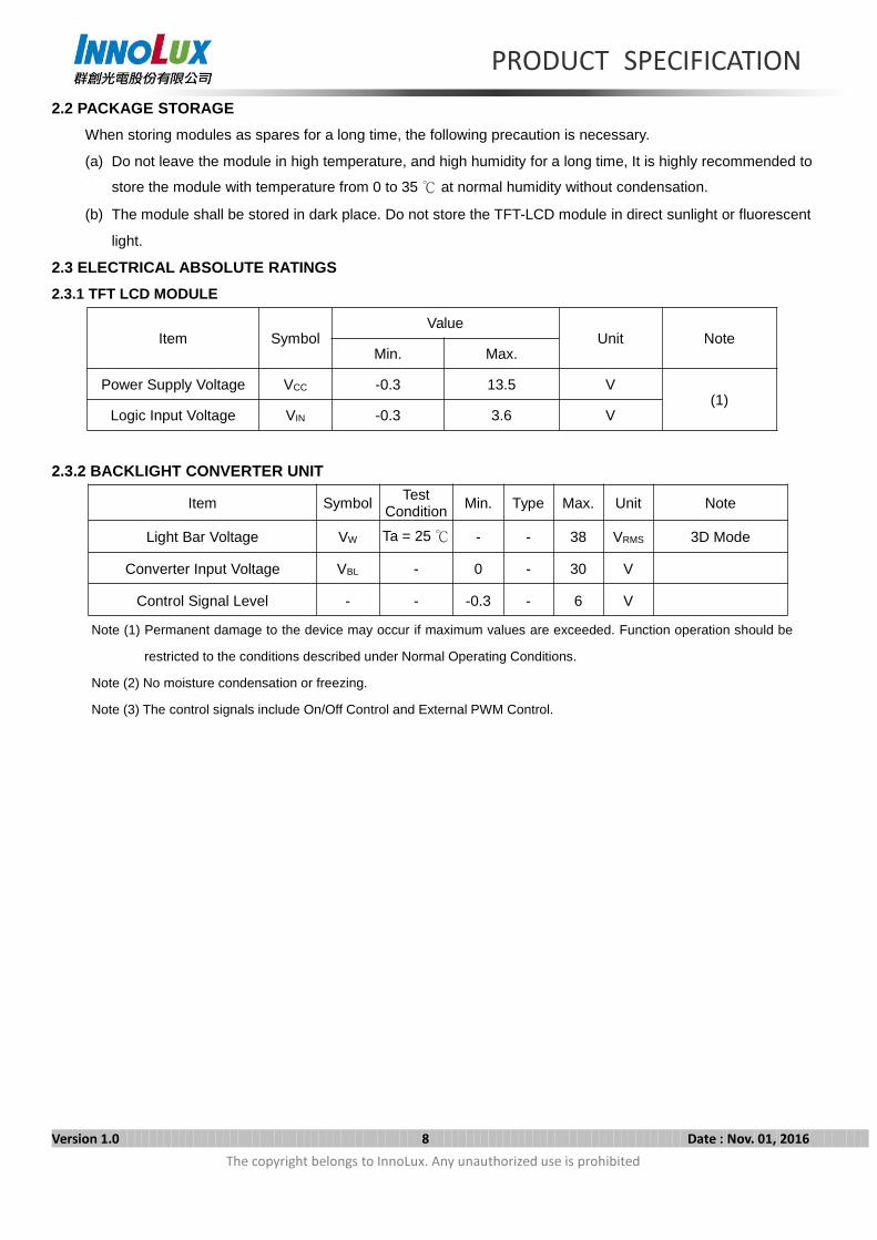
2.3 ELECTRICAL ABSOLUTE RATINGS
2.3.1 TFT LCD MODULE
Item SymbolValue
Unit NoteMin. Max.
Power Supply Voltage VCC -0.3 13.5 V(1)
Logic Input Voltage VIN -0.3 3.6 V
2.3.2 BACKLIGHT CONVERTER UNIT
Item SymbolTest
Condition Min. Type Max. Unit Note
Light Bar Voltage VW Ta = 25 - - 38 VRMS 3D Mode
Converter Input Voltage VBL - 0 - 30 V
Control Signal Level - - -0.3 - 6 V
Note (1) Permanent damage to the device may occur if maximum values are exceeded. Function operation should be
restricted to the conditions described under Normal Operating Conditions.
Note (2) No moisture condensation or freezing.
Note (3) The control signals include On/Off Control and External PWM Control.
PRODUCT SPECIFICATION
Version 1.0 9 Date : Nov. 01, 2016The copyright belongs to InnoLux. Any unauthorized use is prohibited
3. ELECTRICAL CHARACTERISTICS
3.1 TFT LCD MODULE
(Ta = 25 ± 2 ºC)
Parameter SymbolValue
Unit NoteMin. Typ. Max.
Power Supply Voltage VCC 10.8 12 13.2 V (1)
Rush Current IRUSH - - 2.65 A (2)
Power
Consumption
White Pattern PT - 7.26 7.98 W
(3)
Black Pattern PT - 7.04 7.74 W
Horizontal Stripe PT - 13.19 14.51 W
Power
Supply
Current
White Pattern - - 0.63 0.75 A
Black Pattern - - 0.61 0.73 A
Horizontal Stripe - - 1.15 1.38 A
LVDS
interface
Differential InputHighThreshold Voltage
VLVTH - - +100 mV
(4)
Differential InputLowThreshold Voltage
VLVTL -100 - - mV
Common Input
VoltageVCM 1.0 1.2 1.4 V
Differential inputvoltage(single-end)
|VID| 100 - 600 mV
Terminating
ResistorRT - 100 - ohm
CMOS
interface
Input HighThreshold Voltage
VIH 2.7 - 3.6 V
Input Low
Threshold VoltageVIL 0 - 0.7 V
PRODUCT SPECIFICATION
Version 1.0 10 Date : Nov. 01, 2016The copyright belongs to InnoLux. Any unauthorized use is prohibited
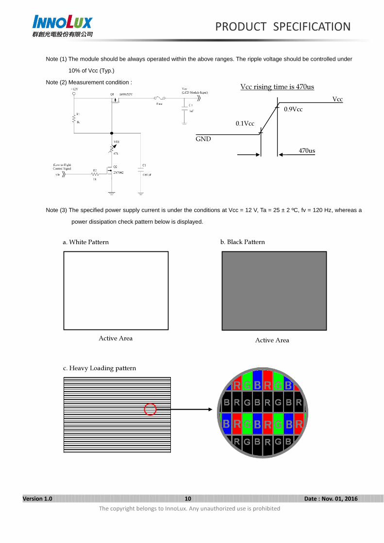
Note (1) The module should be always operated within the above ranges. The ripple voltage should be controlled under
10% of Vcc (Typ.)
Note (2) Measurement condition :
Note (3) The specified power supply current is under the conditions at Vcc = 12 V, Ta = 25 ± 2 ºC, fv = 120 Hz, whereas a
power dissipation check pattern below is displayed.
Vcc rising time is 470us
470us
Vcc
GND
0.9Vcc0.1Vcc
Active Area
b. Black Pattern
Active Area
a. White Pattern
c. Heavy Loading pattern
PRODUCT SPECIFICATION
Version 1.0 11 Date : Nov. 01, 2016The copyright belongs to InnoLux. Any unauthorized use is prohibited
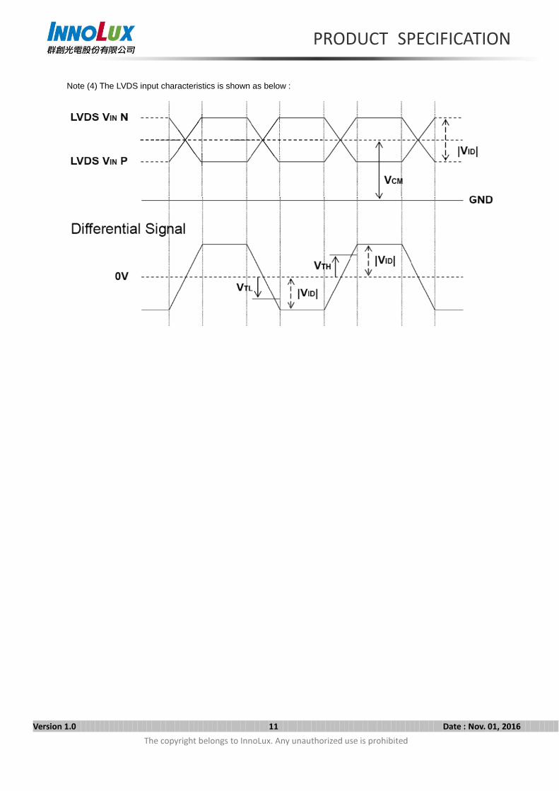
Note (4) The LVDS input characteristics is shown as below :
PRODUCT SPECIFICATION
Version 1.0 12 Date : Nov. 01, 2016The copyright belongs to InnoLux. Any unauthorized use is prohibited
3.2 BACKLIGHT UNIT
3.2.1 CONVERTER CHARACTERISTICS
Parameter SymbolValue
Unit NoteMin. Typ. Max.
Power Consumption PBL(2D) - 130.0 149.5 W (1), (2)
Converter Input Voltage VBL 22.8 24.0 25.2 VDC
Converter Input Current IBL(2D) - 5.42 6.23 A Non Dimming
Input Inrush Current IR(2D) - - 8.5 ApeakVBL=22.8V
(3), (6)
Dimming Frequency FB - 160 - Hz (5)
Dimming Duty Ratio DDR 0 - 100 % (4), (5)
Life Time - 30,000 - - Hrs (7)
Note (1) The power supply capacity should be higher than the total converter power consumption PBL. Since the pulse
width modulation (PWM) mode was applied for backlight dimming, the driving current changed as PWM duty
on and off. The transient response of power supply should be considered for the changing loading when
converter dimming.
Note (2) The measurement condition of Max. value is based on 65" backlight unit under input voltage 24V at 2D Mode
and lighting 1 hour later.
Note (3) For input inrush current measure, the VBL rising time from 10% to 90% is about 20ms.
Note (4) EPWM signal have to input available duty range. Between 97% and 100% duty (DDR) have to be avoided.
(97% < DDR < 100%) But 100% duty (DDR) is possible. 5% duty (DDR) is only valid for electrical operation.
Note (5) FB and DDR are available only at 2D Mode.
Note (6) Below diagram is only for power supply design reference.
PRODUCT SPECIFICATION
Version 1.0 13 Date : Nov. 01, 2016The copyright belongs to InnoLux. Any unauthorized use is prohibited
Note (7) The lifetime is defined as the time which luminance of the LED decays to 50% compared to the initial value,
Operating condition: Continuous operating at Ta = 25±2
PRODUCT SPECIFICATION
Version 1.0 14 Date : Nov. 01, 2016The copyright belongs to InnoLux. Any unauthorized use is prohibited
3.2.2 CONVERTER INTERFACE CHARACTERISTICS
Parameter SymbolTest
Condition
ValueUnit Note
Min. Typ. Max.
On/Off Control VoltageON
VBLON- 2.0 - 5.0 V
OFF - 0 - 0.8 V
External PWM Control
Voltage
HI
VEPWM
- 2.0 - 5.25 V Duty on(5), (6)
LO - 0 - 0.8 V Duty off
External PWM Frequency FEPWM - 150 - 170 Hz Normal mode (7)
Error Signal ERR - - - - - Abnormal: Open
VBL Rising Time Tr1 - 20 - - ms 10%-90%VBL
Control Signal Rising Time Tr - - - 100 ms
Control Signal Falling Time Tf - - - 100 ms
PWM Signal Rising Time TPWMR - - - 50 us(6)
PWM Signal Falling Time TPWMF - - - 50 us
Input Impedance Rin - 1 - - MΩ EPWM, BLON
PWM Delay Time TPWM - 100 - - ms (6)
BLON Delay TimeTon - 300 - - ms
Ton1 - 300 - - ms
BLON Off Time Toff - 300 - - ms
Note (1) The Dimming signal should be valid before backlight turns on by BLON signal. It is inhibited to change the
external PWM signal during backlight turn on period.
Note (2) The power sequence and control signal timing are shown in the Fig.1. For a certain reason, the converter has a
possibility to be damaged with wrong power sequence and control signal timing.
Note (3) While system is turned ON or OFF, the power sequences must follow as below descriptions:
Turn ON sequence: VBL → PWM signal → BLON
Turn OFF sequence: BLOFF → PWM signal → VBL
Note (4) When converter protective function is triggered, ERR will output open collector status. Please refers to Fig.2.
Note (5) The EPWM interface that inserts a pull up resistor to 5V in Max Duty (100%), please refers to Fig.3.
Note (6) EPWM is available only at 2D Mode.
Note (7) EPWM signal have to input available frequency range.
Note (8) [Recommend] EPWM duty ratio is set at 100%(Max. Brightness) in 3D Mode.
PRODUCT SPECIFICATION
Version 1.0 15 Date : Nov. 01, 2016The copyright belongs to InnoLux. Any unauthorized use is prohibited
2.0V0.8V
Tr TfBacklight on duration
0
VEPWM
VW
Ton
100%
ExternalPWM Duty
VBL
VBLON
0
0
2.0V
0.8V
Toff
ExternalPWMPeriod
Tr1
Ext. Dimming Function
TPWMFTPWMR
TPWM
Floating
Ton1
0.9VBL
0.1VBL
Fig. 1
Fig. 2 Fig. 3
PRODUCT SPECIFICATION
Version 1.0 16 Date : Nov. 01, 2016The copyright belongs to InnoLux. Any unauthorized use is prohibited
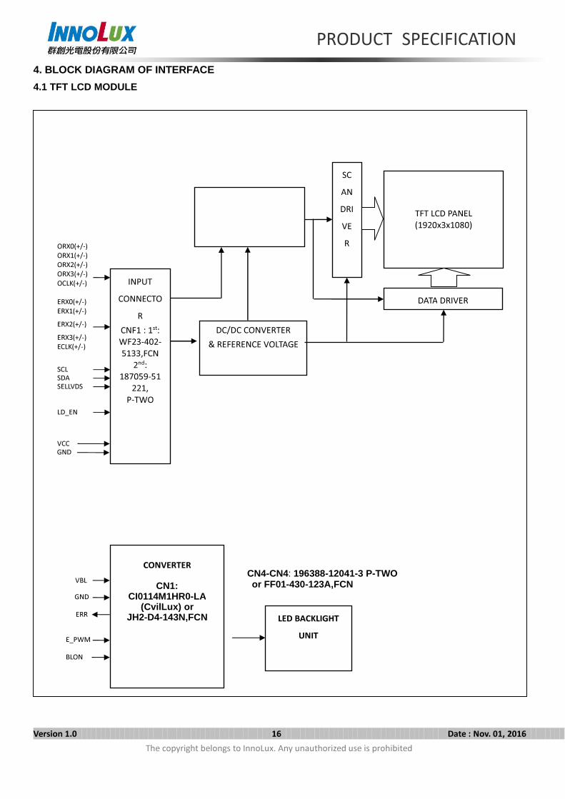
4. BLOCK DIAGRAM OF INTERFACE
4.1 TFT LCD MODULE
SELLVDS
VBLGND
ERR
E_PWMBLON
GND
SDA
CN4-CN4: 196388-12041-3 P-TWOor FF01-430-123A,FCN
ORX0(+/-)ORX1(+/-)ORX2(+/-)ORX3(+/-)OCLK(+/-)
ERX0(+/-)ERX1(+/-)ERX2(+/-)ERX3(+/-)ECLK(+/-)
INPUTCONNECTO
RCNF1 : 1st:WF23-402-5133,FCN
2nd:187059-51
221,P-TWO
TFT LCD PANEL(1920x3x1080)
DATA DRIVER
SCANDRIVER
DC/DC CONVERTER& REFERENCE VOLTAGE
LD_EN
CONVERTER
CN1:CI0114M1HR0-LA
(CvilLux) orJH2-D4-143N,FCN LED BACKLIGHT
UNIT
VCC
SCL
PRODUCT SPECIFICATION
Version 1.0 17 Date : Nov. 01, 2016The copyright belongs to InnoLux. Any unauthorized use is prohibited
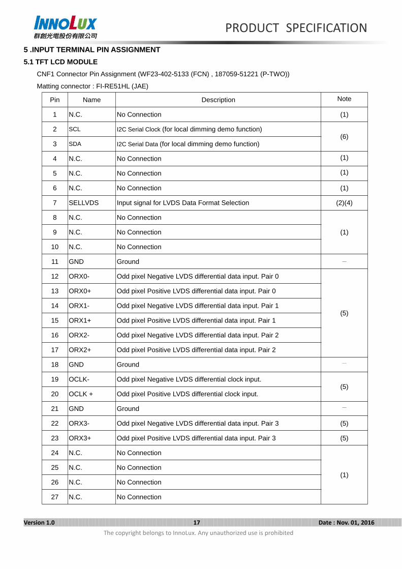
5 .INPUT TERMINAL PIN ASSIGNMENT
5.1 TFT LCD MODULE
CNF1 Connector Pin Assignment (WF23-402-5133 (FCN) , 187059-51221 (P-TWO))
Matting connector : FI-RE51HL (JAE)
Pin Name Description Note
1 N.C. No Connection (1)
2 SCL I2C Serial Clock (for local dimming demo function)(6)
3 SDA I2C Serial Data (for local dimming demo function)
4 N.C. No Connection (1)
5 N.C. No Connection (1)
6 N.C. No Connection (1)
7 SELLVDS Input signal for LVDS Data Format Selection (2)(4)
8 N.C. No Connection
(1)9 N.C. No Connection
10 N.C. No Connection
11 GND Ground -
12 ORX0- Odd pixel Negative LVDS differential data input. Pair 0
(5)
13 ORX0+ Odd pixel Positive LVDS differential data input. Pair 0
14 ORX1- Odd pixel Negative LVDS differential data input. Pair 1
15 ORX1+ Odd pixel Positive LVDS differential data input. Pair 1
16 ORX2- Odd pixel Negative LVDS differential data input. Pair 2
17 ORX2+ Odd pixel Positive LVDS differential data input. Pair 2
18 GND Ground -
19 OCLK- Odd pixel Negative LVDS differential clock input.(5)
20 OCLK + Odd pixel Positive LVDS differential clock input.
21 GND Ground -
22 ORX3- Odd pixel Negative LVDS differential data input. Pair 3 (5)
23 ORX3+ Odd pixel Positive LVDS differential data input. Pair 3 (5)
24 N.C. No Connection
(1)25 N.C. No Connection
26 N.C. No Connection
27 N.C. No Connection
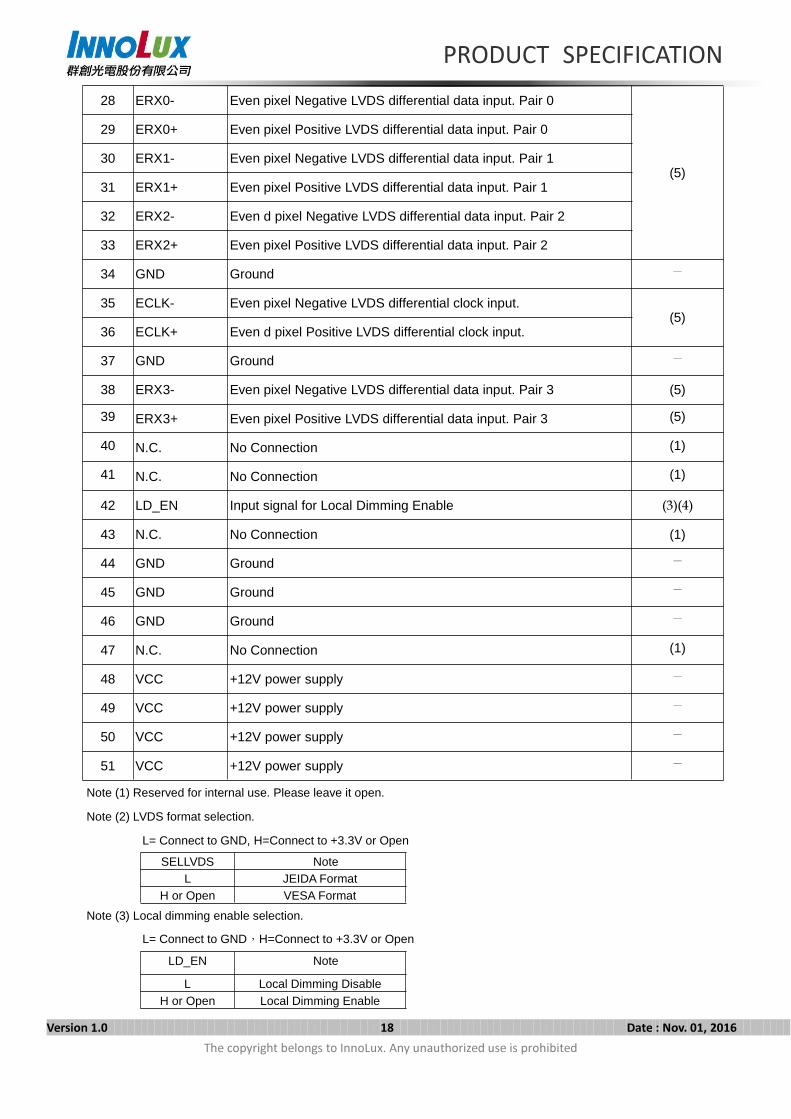
PRODUCT SPECIFICATION
Version 1.0 18 Date : Nov. 01, 2016The copyright belongs to InnoLux. Any unauthorized use is prohibited
28 ERX0- Even pixel Negative LVDS differential data input. Pair 0
(5)
29 ERX0+ Even pixel Positive LVDS differential data input. Pair 0
30 ERX1- Even pixel Negative LVDS differential data input. Pair 1
31 ERX1+ Even pixel Positive LVDS differential data input. Pair 1
32 ERX2- Even d pixel Negative LVDS differential data input. Pair 2
33 ERX2+ Even pixel Positive LVDS differential data input. Pair 2
34 GND Ground -
35 ECLK- Even pixel Negative LVDS differential clock input.(5)
36 ECLK+ Even d pixel Positive LVDS differential clock input.
37 GND Ground -
38 ERX3- Even pixel Negative LVDS differential data input. Pair 3 (5)
39 ERX3+ Even pixel Positive LVDS differential data input. Pair 3 (5)
40 N.C. No Connection (1)
41 N.C. No Connection (1)
42 LD_EN Input signal for Local Dimming Enable (3)(4)43 N.C. No Connection (1)
44 GND Ground -
45 GND Ground -
46 GND Ground -
47 N.C. No Connection (1)
48 VCC +12V power supply -
49 VCC +12V power supply -
50 VCC +12V power supply -
51 VCC +12V power supply -
Note (1) Reserved for internal use. Please leave it open.
Note (2) LVDS format selection.
L= Connect to GND, H=Connect to +3.3V or Open
SELLVDS NoteL JEIDA Format
H or Open VESA Format
Note (3) Local dimming enable selection.
L= Connect to GND,H=Connect to +3.3V or Open
LD_EN Note
L Local Dimming DisableH or Open Local Dimming Enable
PRODUCT SPECIFICATION
Version 1.0 19 Date : Nov. 01, 2016The copyright belongs to InnoLux. Any unauthorized use is prohibited
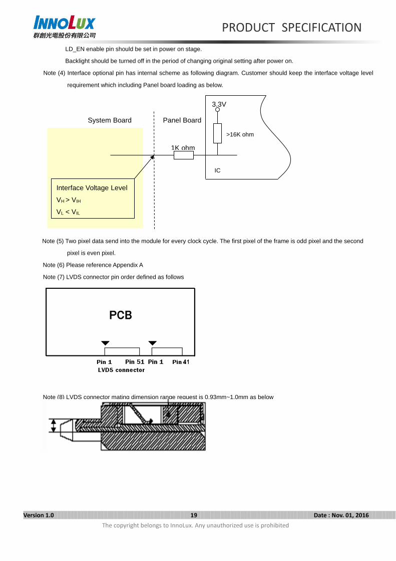
LD_EN enable pin should be set in power on stage.
Backlight should be turned off in the period of changing original setting after power on.
Note (4) Interface optional pin has internal scheme as following diagram. Customer should keep the interface voltage level
requirement which including Panel board loading as below.
IC
>16K ohm
1K ohm
Panel BoardSystem Board
Interface Voltage Level
VH > VIH
VL < VIL
3.3V
Note (5) Two pixel data send into the module for every clock cycle. The first pixel of the frame is odd pixel and the second
pixel is even pixel.
Note (6) Please reference Appendix A
Note (7) LVDS connector pin order defined as follows
Note (8) LVDS connector mating dimension range request is 0.93mm~1.0mm as below
PRODUCT SPECIFICATION
Version 1.0 20 Date : Nov. 01, 2016The copyright belongs to InnoLux. Any unauthorized use is prohibited
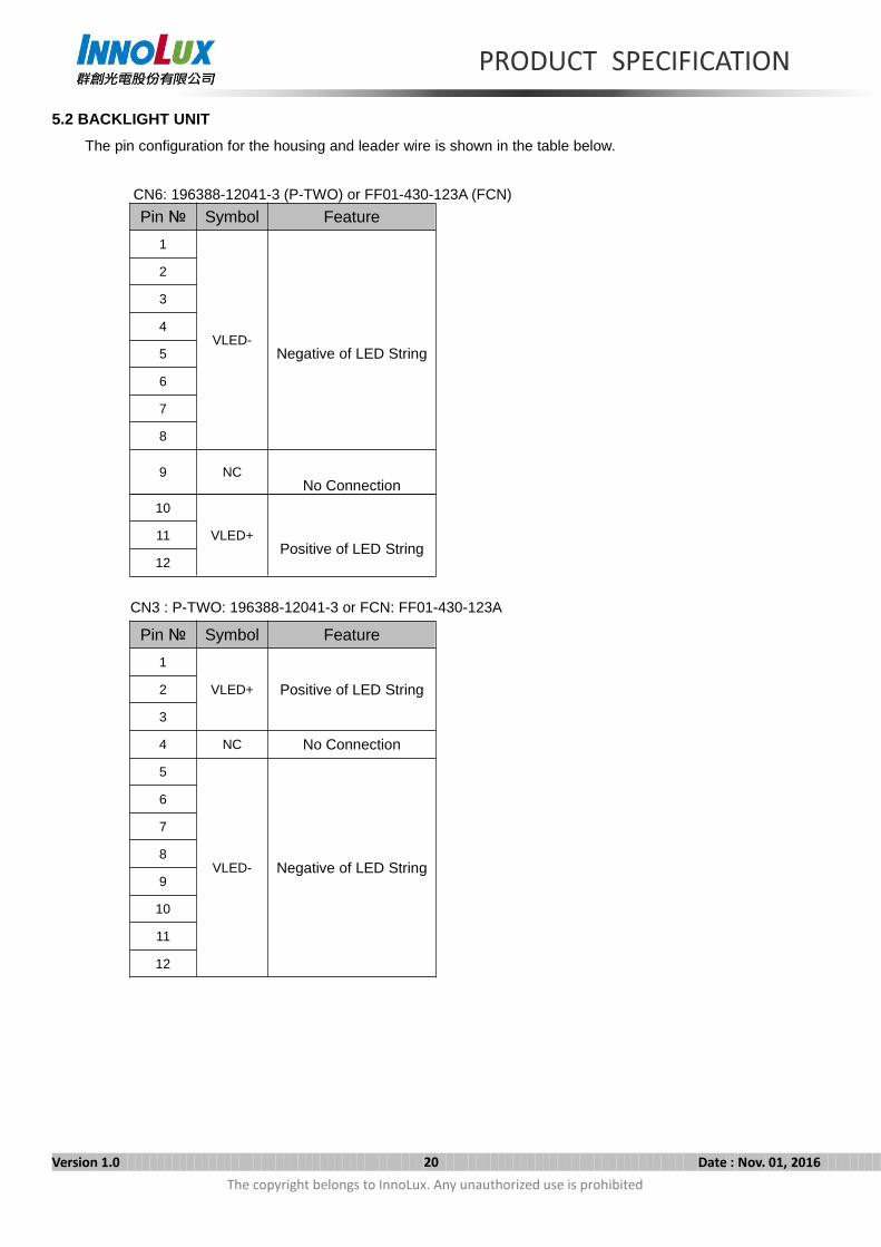
5.2 BACKLIGHT UNIT
The pin configuration for the housing and leader wire is shown in the table below.
CN6: 196388-12041-3 (P-TWO) or FF01-430-123A (FCN)
Pin Symbol Feature
1
VLED-Negative of LED String
2
3
4
5
6
7
8
9 NCNo Connection
10
VLED+Positive of LED String
11
12
CN3 : P-TWO: 196388-12041-3 or FCN: FF01-430-123A
Pin Symbol Feature
1
VLED+ Positive of LED String2
3
4 NC No Connection
5
VLED- Negative of LED String
6
7
8
9
10
11
12
PRODUCT SPECIFICATION
Version 1.0 21 Date : Nov. 01, 2016The copyright belongs to InnoLux. Any unauthorized use is prohibited
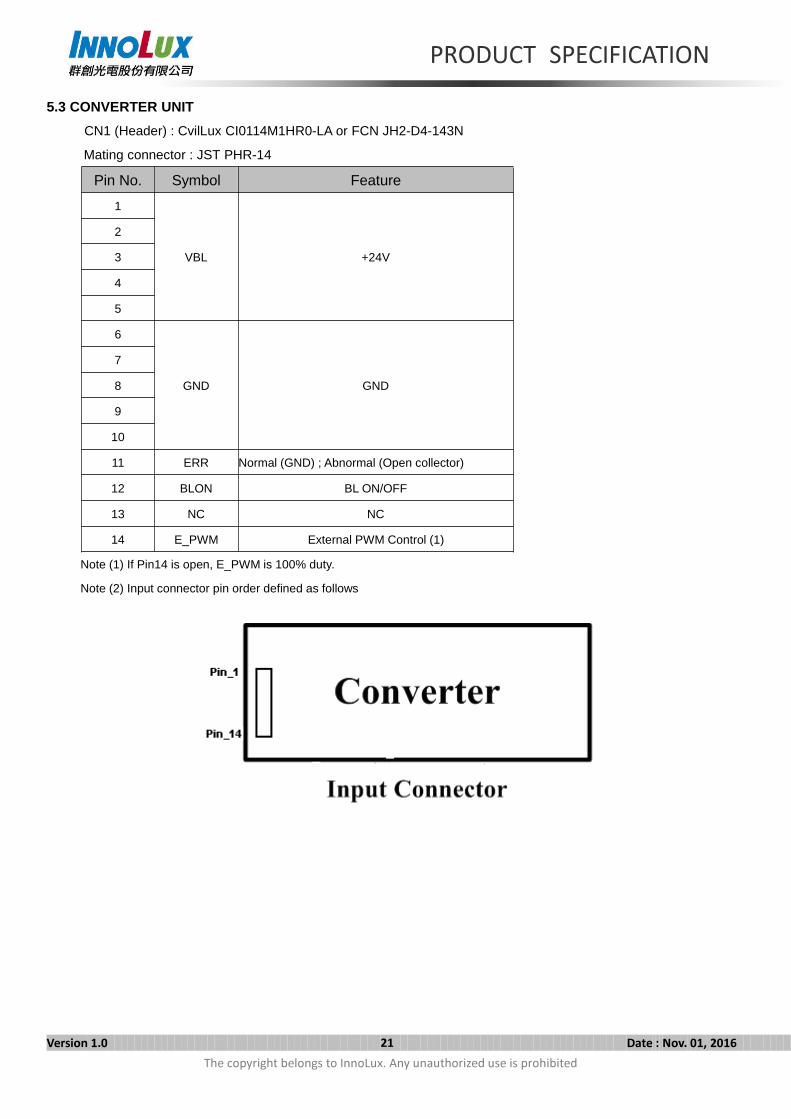
5.3 CONVERTER UNIT
CN1 (Header) : CvilLux CI0114M1HR0-LA or FCN JH2-D4-143N
Mating connector : JST PHR-14
Pin No. Symbol Feature
1
VBL +24V
2
3
4
5
6
GND GND
7
8
9
10
11 ERR Normal (GND) ; Abnormal (Open collector)
12 BLON BL ON/OFF
13 NC NC
14 E_PWM External PWM Control (1)
Note (1) If Pin14 is open, E_PWM is 100% duty.
Note (2) Input connector pin order defined as follows
PRODUCT SPECIFICATION
Version 1.0 22 Date : Nov. 01, 2016The copyright belongs to InnoLux. Any unauthorized use is prohibited
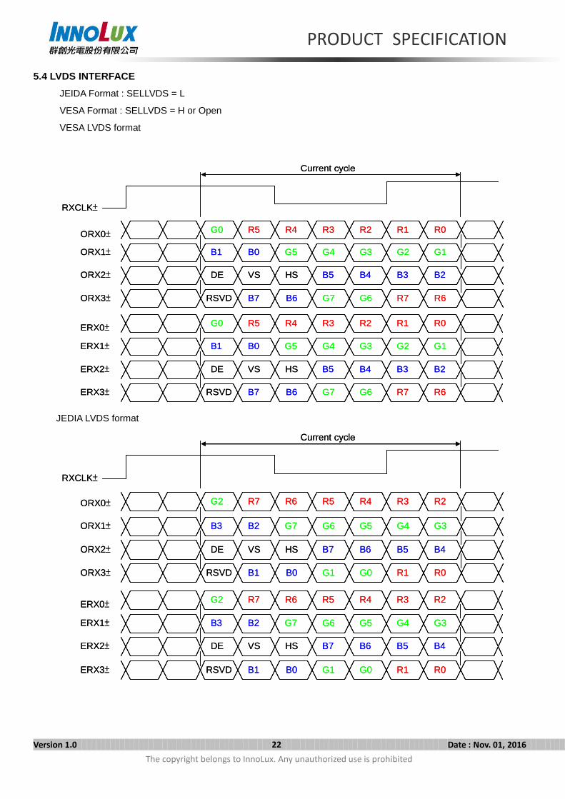
5.4 LVDS INTERFACE
JEIDA Format : SELLVDS = L
VESA Format : SELLVDS = H or Open
VESA LVDS format
G1
R0
G3 G2G4
R5G0 R4 R3 R2 R1
B0 G5B1
B2B4 B3B5VS HSDE
R6G6 R7G7B7 B6RSVD
RXCLK±
ORX0±
ORX1±
ORX3±
ORX2±
Current cycle
G1
R0
G3 G2G4
R5G0 R4 R3 R2 R1
B0 G5B1
B2B4 B3B5VS HSDE
R6G6 R7G7B7 B6RSVD
ERX0±
ERX1±
ERX3±
ERX2±
G1
R0
G3 G2G4
R5G0 R4 R3 R2 R1
B0 G5B1
B2B4 B3B5VS HSDE
R6G6 R7G7B7 B6RSVD
RXCLK±
ORX0±
ORX1±
ORX3±
ORX2±
Current cycle
G1
R0
G3 G2G4
R5G0 R4 R3 R2 R1
B0 G5B1
B2B4 B3B5VS HSDE
R6G6 R7G7B7 B6RSVD
ERX0±
ERX1±
ERX3±
ERX2±
JEDIA LVDS format
Current cycle
G3
R2
G5 G4G6
R7G2 R6 R5 R4 R3
B2 G7B3
B4B6 B5B7VS HSDE
R0G0 R1G1B1 B0RSVD
RXCLK±
ORX0±
ORX1±
ORX3±
ORX2±
G3
R2
G5 G4G6
R7G2 R6 R5 R4 R3
B2 G7B3
B4B6 B5B7VS HSDE
R0G0 R1G1B1 B0RSVD
ERX0±
ERX1±
ERX3±
ERX2±
Current cycle
G3
R2
G5 G4G6
R7G2 R6 R5 R4 R3
B2 G7B3
B4B6 B5B7VS HSDE
R0G0 R1G1B1 B0RSVD
RXCLK±
ORX0±
ORX1±
ORX3±
ORX2±
G3
R2
G5 G4G6
R7G2 R6 R5 R4 R3
B2 G7B3
B4B6 B5B7VS HSDE
R0G0 R1G1B1 B0RSVD
ERX0±
ERX1±
ERX3±
ERX2±
PRODUCT SPECIFICATION
Version 1.0 23 Date : Nov. 01, 2016The copyright belongs to InnoLux. Any unauthorized use is prohibited
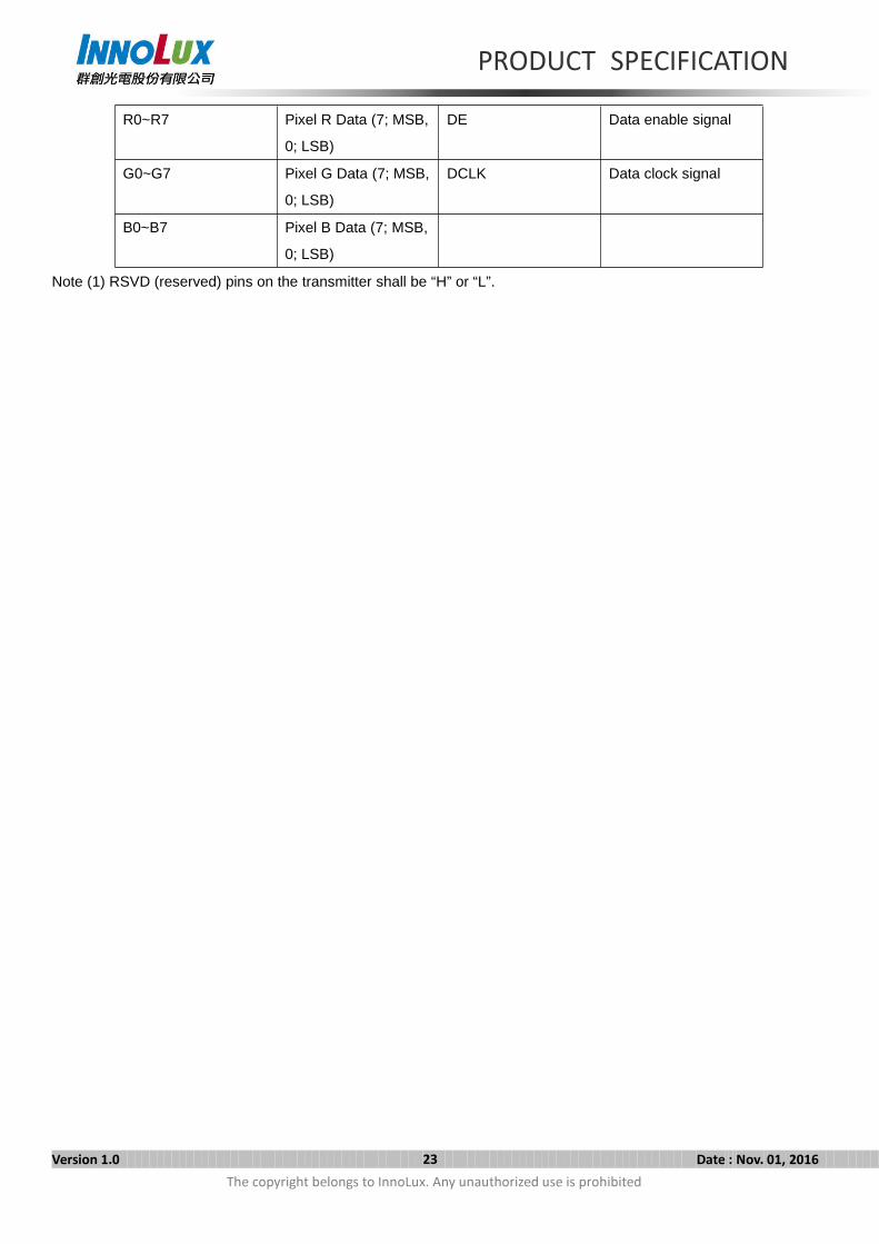
R0~R7 Pixel R Data (7; MSB,
0; LSB)
DE Data enable signal
G0~G7 Pixel G Data (7; MSB,
0; LSB)
DCLK Data clock signal
B0~B7 Pixel B Data (7; MSB,
0; LSB)
Note (1) RSVD (reserved) pins on the transmitter shall be “H” or “L”.

PRODUCT SPECIFICATION
Version 1.0 24 Date : Nov. 01, 2016The copyright belongs to InnoLux. Any unauthorized use is prohibited
5.5 COLOR DATA INPUT ASSIGNMENT
The brightness of each primary color (red, green and blue) is based on the 8-bit gray scale data input for the color.
The higher the binary input the brighter the color. The table below provides the assignment of color versus data
input.
ColorData Signal
Red Green BlueR7 R6 R5 R4 R3 R2 R1 R0 G7 G6 G5 G4 G3 G2 G1 G0 B7 B6 B5 B4 B3 B2 B1 B0
BasicColors
BlackRedGreenBlueCyanMagentaYellowWhite
01000111
01000111
01000111
01000111
01000111
01000111
01000111
01000111
00101011
00101011
00101011
00101011
00101011
00101011
00101011
00101011
00011101
00011101
00011101
00011101
00011101
00011101
00011101
00011101
GrayScaleOfRed
Red (0) / DarkRed (1)Red (2)
::
Red (253)Red (254)Red (255)
000::111
000::111
000::111
000::111
000::111
001::011
010::101
000::111
000::000
000::000
000::000
000::000
000::000
000::000
000::000
000::000
000::000
000::000
000::000
000::000
000::000
000::000
000::000
000::000
GrayScaleOfGreen
Green (0) / DarkGreen (1)Green (2)
::
Green (253)Green (254)Green (255)
000::000
000::000
000::000
000::000
000::000
000::000
000::000
000::000
000::111
000::111
000::111
000::111
000::111
001::011
010::101
000::111
000::000
000::000
000::000
000::000
000::000
000::000
000::000
000::000
GrayScaleOfBlue
Blue (0) / DarkBlue (1)Blue (2)
::
Blue (253)Blue (254)Blue (255)
000::000
000::000
000::000
000::000
000::000
000::000
000::000
000::000
000::000
000::000
000::000
000::000
000::000
000::000
000::000
000::000
000::111
000::111
000::111
000::111
000::111
000::111
001::011
010::101
Note (1) 0: Low Level Voltage,1: High Level Voltage
PRODUCT SPECIFICATION
Version 1.0 25 Date : Nov. 01, 2016The copyright belongs to InnoLux. Any unauthorized use is prohibited
6. INTERFACE TIMING
6.1 INPUT SIGNAL TIMING SPECIFICATIONS
The input signal timing specifications are shown as the following table and timing diagram. (Ta = 25 ± 2 ºC)
Signal Item Symbol Min. Typ. Max. Unit Note
LVDS
Receiver
Clock
FrequencyFclkin
(=1/TC)60 74.25 79 MHz
Input cycle to
cycle jitterTrcl - - 200 ps (3)
Spread spectrum
modulation rangeFclkin_mod Fclkin-2% - Fclkin+2% MHz
(4)Spread spectrum
modulation frequencyFSSM - - 200 KHz
LVDS
Receiver
Data
Receiver Skew Margin TRSKM -400 - 400 ps (5)
6.1.1 Timing spec for Frame Rate = 50Hz
Signal Item Symbol Min. Typ. Max. Unit NoteFrame rate Frame rate Fr5 47 50 53 Hz (6),(7)
VerticalActive
DisplayTerm
Total Tv 1115 1350 1380 Th Tv=Tvd+TvbDisplay Tvd 1080 1080 1080 Th -
Blank Tvb 35 270 300 Th -
HorizontalActive
DisplayTerm
Total Th 1050 1100 1150 Tc Th=Thd+Thb
Display Thd 960 960 960 Tc -
Blank Thb 90 140 190 Tc -
PRODUCT SPECIFICATION
Version 1.0 26 Date : Nov. 01, 2016The copyright belongs to InnoLux. Any unauthorized use is prohibited
6.1.2 Timing spec for Frame Rate = 60Hz
Signal Item Symbol Min. Typ. Max. Unit NoteFrame rate 2D mode Fr6 57 60 63 Hz (6),(7)
VerticalActive
DisplayTerm
2D ModeTotal Tv 1115 1125 1380 Th Tv=Tvd+TvbDisplay Tvd 1080 1080 1080 Th -
Blank Tvb 35 45 300 Th -
HorizontalActive
DisplayTerm
2D ModeTotal Th 1050 1100 1150 Tc Th=Thd+ThbDisplay Thd 960 960 960 Tc -
Blank Thb 90 140 190 Tc -
Note (1) Since the module is operated in DE only mode, Hsync and Vsync input signals should be set to low logic level.
Otherwise, this module would operate abnormally.
Note (2) Please make sure the range of pixel clock has follow the below equation:
Fclkin(max) ≧ Fr6 Tv Th
Fr5 Tv Th ≧ Fclkin(min)
INPUT SIGNAL TIMING DIAGRAM
Tv
Tvd Tvb
Th
DE
Thb
Valid Display Data (960 clocks)
Tc
DCLK
Thd
DE
DATA
PRODUCT SPECIFICATION
Version 1.0 27 Date : Nov. 01, 2016The copyright belongs to InnoLux. Any unauthorized use is prohibited
Note (3) The input clock cycle-to-cycle jitter is defined as below figures. Trcl =|T1 – T︱
PRODUCT SPECIFICATION
Version 1.0 28 Date : Nov. 01, 2016The copyright belongs to InnoLux. Any unauthorized use is prohibited
Note (4) The SSCG (Spread spectrum clock generator) is defined as below figures.
Note (5) The LVDS timing diagram and the receiver skew margin is defined and shown in following figure.
Note (6) The frame-to-frame jitter of the input frame rate is defined as the following figures. FRn = FRn-1 ± 0.07Hz.Note (7) The setup of the frame rate jitter > 0.07Hz may result in the cosmetic of panel symptom but the electric function is notaffected.
RXCLK+/-
RXn+/-
TRSKM
Tc
PRODUCT SPECIFICATION
Version 1.0 29 Date : Nov. 01, 2016The copyright belongs to InnoLux. Any unauthorized use is prohibited
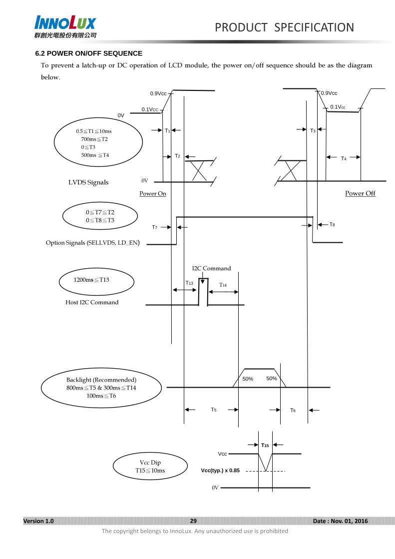
6.2 POWER ON/OFF SEQUENCE
To prevent a latch-up or DC operation of LCD module, the power on/off sequence should be as the diagrambelow.
Backlight (Recommended)800ms≦T5 & 300ms≦T14
100ms≦T6
Power Off
50%
0V
0V
T6
T3T1
0.1Vcc
T4T2
Power On
T8
0V
Vcc(typ.) x 0.85Vcc Dip
T15≦10ms
Vcc
T15
T13
I2C Command
0.1VCC
T7
0.9Vcc 0.9Vcc
0.5≦T1≦10ms700ms≦T20≦T3500ms ≦T4
50%
T5
LVDS Signals
0≦T7≦T20≦T8≦T3
T14
Host I2C Command
1200ms≦T13
Option Signals (SELLVDS, LD_EN)
PRODUCT SPECIFICATION
Version 1.0 30 Date : Nov. 01, 2016The copyright belongs to InnoLux. Any unauthorized use is prohibited
Note (1) The supply voltage of the external system for the module input should follow the definition of Vcc.Note (2) Apply the LED voltage within the LCD operation range. When the backlight turns on before the LCD operation or
the LCD turns off before the backlight turns off, the display may momentarily become abnormal screen.Note (3) In case of Vcc is in off level, please keep the level of input signals on the low or high impedance. If T2<0,that maybe
cause electrical overstress failure.Note (4) T4 should be measured after the module has been fully discharged between power off and on period.Note (5) Interface signal shall not be kept at high impedance when the power is on.Note (6) Vcc must decay smoothly when power-off.
PRODUCT SPECIFICATION
Version 1.0 31 Date : Nov. 01, 2016The copyright belongs to InnoLux. Any unauthorized use is prohibited
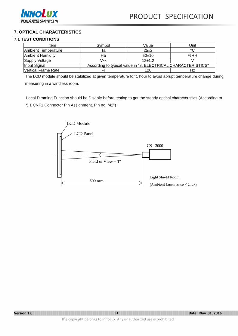
7. OPTICAL CHARACTERISTICS
7.1 TEST CONDITIONSItem Symbol Value Unit
Ambient Temperature Ta 25±2 oCAmbient Humidity Ha 50±10 %RHSupply Voltage VCC 12±1.2 VInput Signal According to typical value in "3. ELECTRICAL CHARACTERISTICS"Vertical Frame Rate Fr 120 Hz
The LCD module should be stabilized at given temperature for 1 hour to avoid abrupt temperature change during
measuring in a windless room.
Local Dimming Function should be Disable before testing to get the steady optical characteristics (According to
5.1 CNF1 Connector Pin Assignment, Pin no. “42”)
CS - 2000
500 mm
LCD Module
LCD Panel
Field of View = 1º
Light Shield Room(Ambient Luminance < 2 lux)
PRODUCT SPECIFICATION
Version 1.0 32 Date : Nov. 01, 2016The copyright belongs to InnoLux. Any unauthorized use is prohibited
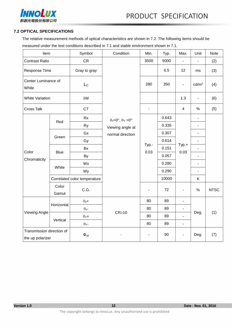
7.2 OPTICAL SPECIFICATIONS
The relative measurement methods of optical characteristics are shown in 7.2. The following items should be
measured under the test conditions described in 7.1 and stable environment shown in 7.1.
Item Symbol Condition Min. Typ. Max. Unit Note
Contrast Ratio CR
θx=0°, θY =0°
Viewing angle at
normal direction
3500 5000 - - (2)
Response Time Gray to gray 6.5 12 ms (3)
Center Luminance of
WhiteLC 280 350 - cd/m2 (4)
White Variation δW 1.3 - (6)
Cross Talk CT - 4 % (5)
Color
Chromaticity
RedRx
Typ.-
0.03
0.643
Typ.+
0.03
-
Ry 0.335 -
GreenGx 0.307 -
Gy 0.614 -
BlueBx 0.151 -
By 0.057 -
WhiteWx 0.280 -
Wy 0.290 -
Correlated color temperature 10000 K
Color
GamutC.G. - 72 - % NTSC
Viewing Angle
Horizontalθx+
CR≥10
80 89 -
Deg. (1)θx- 80 89 -
VerticalθY+ 80 89 -
θY- 80 89 -
Transmission direction of
the up polarizerΦup - - 90 - Deg. (7)
PRODUCT SPECIFICATION
Version 1.0 33 Date : Nov. 01, 2016The copyright belongs to InnoLux. Any unauthorized use is prohibited
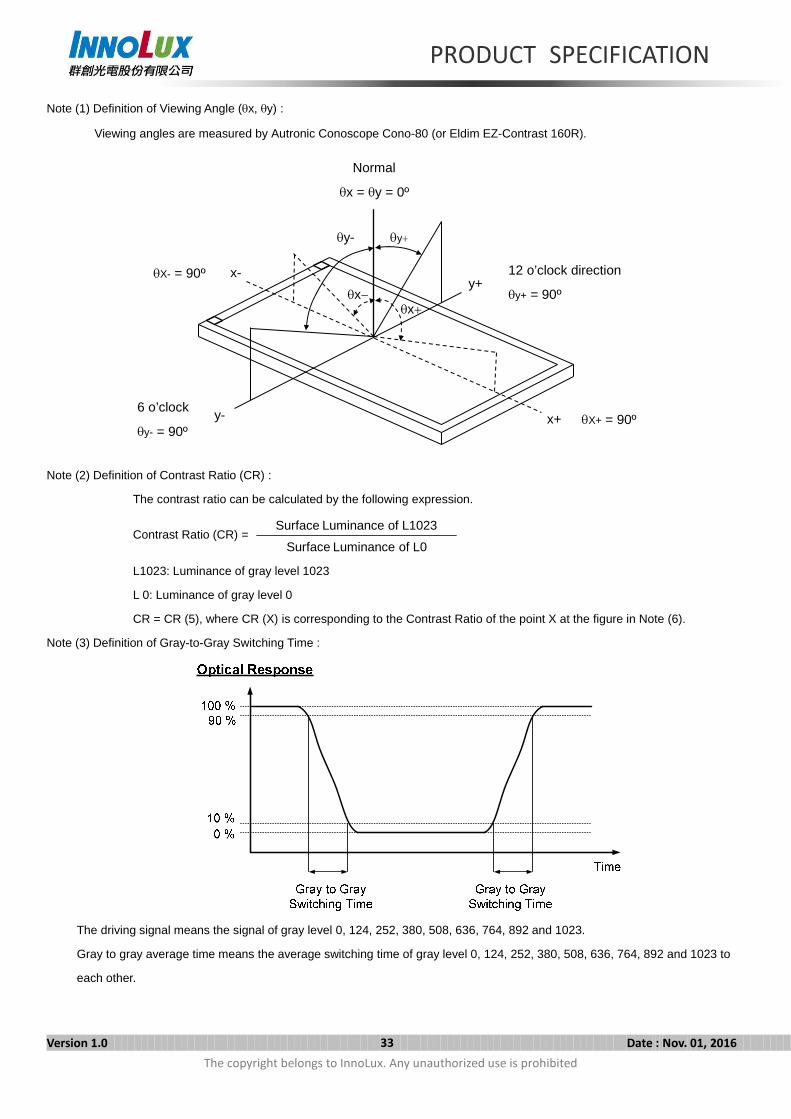
Note (1) Definition of Viewing Angle (θx, θy) :
Viewing angles are measured by Autronic Conoscope Cono-80 (or Eldim EZ-Contrast 160R).
Note (2) Definition of Contrast Ratio (CR) :
The contrast ratio can be calculated by the following expression.
Contrast Ratio (CR) = L0 of Luminance Surface
L1023 of Luminance Surface
L1023: Luminance of gray level 1023
L 0: Luminance of gray level 0
CR = CR (5), where CR (X) is corresponding to the Contrast Ratio of the point X at the figure in Note (6).
Note (3) Definition of Gray-to-Gray Switching Time :
The driving signal means the signal of gray level 0, 124, 252, 380, 508, 636, 764, 892 and 1023.
Gray to gray average time means the average switching time of gray level 0, 124, 252, 380, 508, 636, 764, 892 and 1023 to
each other.
12 o’clock direction
θy+ = 90º
6 o’clock
θy- = 90º
θx−θx+
θy- θy+
x-y+
y- x+
Normal
θx = θy = 0º
θX+ = 90º
θX- = 90º
PRODUCT SPECIFICATION
Version 1.0 34 Date : Nov. 01, 2016The copyright belongs to InnoLux. Any unauthorized use is prohibited
Note (4) Definition of Luminance of White (LC) :
Measure the luminance of gray level 1023 at center point.
LC = L (5), where L (x) is corresponding to the luminance of the point X at the figure in Note (6).
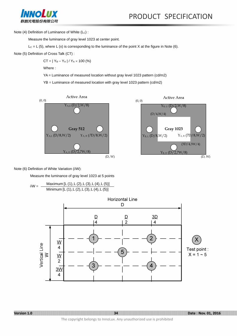
Note (5) Definition of Cross Talk (CT) :
CT = | YB – YA | / YA × 100 (%)
Where :
YA = Luminance of measured location without gray level 1023 pattern (cd/m2)
YB = Luminance of measured location with gray level 1023 pattern (cd/m2)
Note (6) Definition of White Variation (δW):
Measure the luminance of gray level 1023 at 5 points
δW =(5)] L (4), L (3), L (2), L (1), [L Minimum
(5)] L (4), L (3), L (2), L (1), [L Maximum
1 2
3 4
5
D4
D2
3D4
W4W2
3W4
Horizontal Line D
XTest point : X = 1 ~ 5
Active Area
YA, R (7D/8,W/2)
YA, D (D/2,7W/8)
(0, 0)
(D, W)
Gray 512
Active AreaYB, U (D/2,W/8)
(0, 0)
YB, D (D/2,7W/8)
YB, L (D/8,W/2)Gray 1023
YA,U (D/2,W/8)
YA,L (D/8,W/2) YA, R (7D/8,W/2)
(D/4,W/4)
(3D/4,3W/4)
(D, W)
PRODUCT SPECIFICATION
Version 1.0 35 Date : Nov. 01, 2016The copyright belongs to InnoLux. Any unauthorized use is prohibited
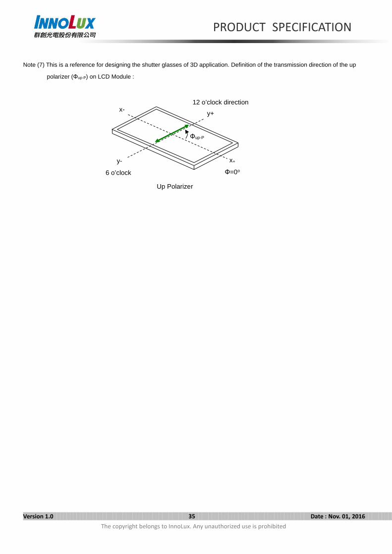
Note (7) This is a reference for designing the shutter glasses of 3D application. Definition of the transmission direction of the up
polarizer (Φup-P) on LCD Module :
y+
6 o’clock
x-
x+
Φ=0o
y-
Φup-P
12 o’clock direction
Up Polarizer
PRODUCT SPECIFICATION
Version 1.0 36 Date : Nov. 01, 2016The copyright belongs to InnoLux. Any unauthorized use is prohibited
8. PRECAUTIONS
8.1 ASSEMBLY AND HANDLING PRECAUTIONS
[1] Do not apply rough force such as bending or twisting to the module during assembly.
[2] Do not apply pressure or impulse to the module to prevent the damage of LCD panel and Backlight.
[3] Bezel of Set can not press or touch the panel surface. It will make light leakage or scrape.
[4] It should be attached to the system firmly using all mounting holes.
[5] It is recommended to assemble or to install a module into the user’s system in clean working areas. The dust
and oil may cause electrical short or worsen the polarizer, do not press or scratch the surface harder than a HB
pencil lead.
[6] Use finger-stalls with soft gloves in order to keep display clean during the incoming inspection and assembly
process.
[7] Protection film for polarizer on the module should be slowly peeled off just before use so that the electrostatic
charge can be minimized.
[8] Do not disassemble the module.
[9] Always follow the correct power-on sequence when the LCD module is turned on. This can prevent the damage
and latch-up of the CMOS LSI chips.
[10] Do not plug in or pull out the I/F connector while the module is in operation, pins of I/F connector should not be
touched directly with bare hands. Do not adjust the variable resistor located on the module.
[11] Moisture can easily penetrate into LCD module and may cause the damage during operation.
[12] When storing modules as spares for a long time, the following precaution is necessary.
[12.1] Do not leave the module in high temperature, and high humidity for a long time. It is highly
recommended to store the module with temperature from 0 to 35 at normal humidity (under 70%)
without condensation.
[12.2] The module shall be stored in dark place. Do not store the TFT-LCD module in direct sunlight or
fluorescent light.
[13] When ambient temperature is lower than 10ºC, the display quality might be reduced. For example, the
response time will become slow, and the starting voltage of LED will be higher than that of room
temperature.
8.2 SAFETY PRECAUTIONS
[1] The startup voltage of a Backlight may cause an electrical shock while assembling with the converter. Do not
disassemble the module or insert anything into the Backlight unit.
[2] Do not connect or disconnect the module in the “Power On” condition.
[3] Do not exceed the absolute maximum rating value. (supply voltage variation, input voltage variation, variation
in part contents and environmental temperature…) Otherwise the module may be damaged.
[4] If the liquid crystal material leaks from the panel, it should be kept away from the eyes or mouth. In case of
contact with hands, skin or clothes, it has to be washed away thoroughly with soap.
[5] Ultra-violet ray filter is necessary for outdoor operation.
8.3 SAFETY STANDARDS
The LCD module should be certified with safety regulations as follows:
PRODUCT SPECIFICATION
Version 1.0 37 Date : Nov. 01, 2016The copyright belongs to InnoLux. Any unauthorized use is prohibited
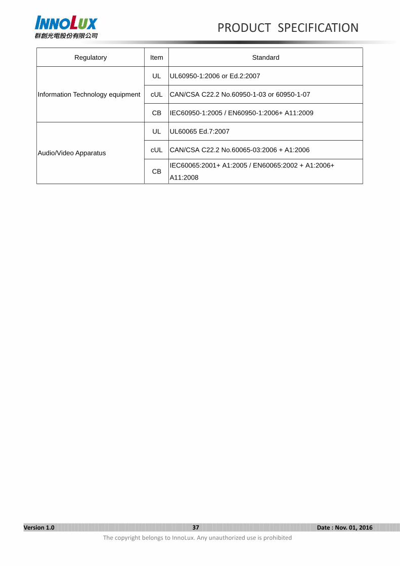
Regulatory Item Standard
Information Technology equipment
UL UL60950-1:2006 or Ed.2:2007
cUL CAN/CSA C22.2 No.60950-1-03 or 60950-1-07
CB IEC60950-1:2005 / EN60950-1:2006+ A11:2009
Audio/Video Apparatus
UL UL60065 Ed.7:2007
cUL CAN/CSA C22.2 No.60065-03:2006 + A1:2006
CBIEC60065:2001+ A1:2005 / EN60065:2002 + A1:2006+
A11:2008
PRODUCT SPECIFICATION
Version 1.0 38 Date : Nov. 01, 2016The copyright belongs to InnoLux. Any unauthorized use is prohibited
9. DEFINITION OF LABELS
9.1 MODULE LABEL
The barcode nameplate is pasted on each module as illustration, and its definitions are as following explanation.
Model Name : S650HJ2-LS5
Revision : Rev. XX, for example: A0, A1… B1, B2… or C1, C2…etc.
Serial ID : X X X X X X X Y M D L N N N N
Serial ID includes the information as below:
Manufactured Date:
Year : 2001=1, 2002=2, 2003=3, 2004=4…2010=0, 2011=1, 2012=2…
Month: 1~9, A~C, for Jan. ~ Dec.
Day: 1~9, A~Y, for 1st to 31st, exclude I ,O, and U.
Revision Code : Cover all the change
Serial No. : Manufacturing sequence of product
Product Line : 1 → Line1, 2 → Line 2, …etc.
Product Line
Year, Month, DateINX Internal Use
INX Internal Use
RevisionINX Internal Use
Serial No.
MADE IN CHINA
LEOO(CAPG/CANO/VIRO)
RoHSX X X X X X X Y M D L N N N N
S650HJ2-LS5 Rev. XX
PRODUCT SPECIFICATION
Version 1.0 39 Date : Nov. 01, 2016The copyright belongs to InnoLux. Any unauthorized use is prohibited
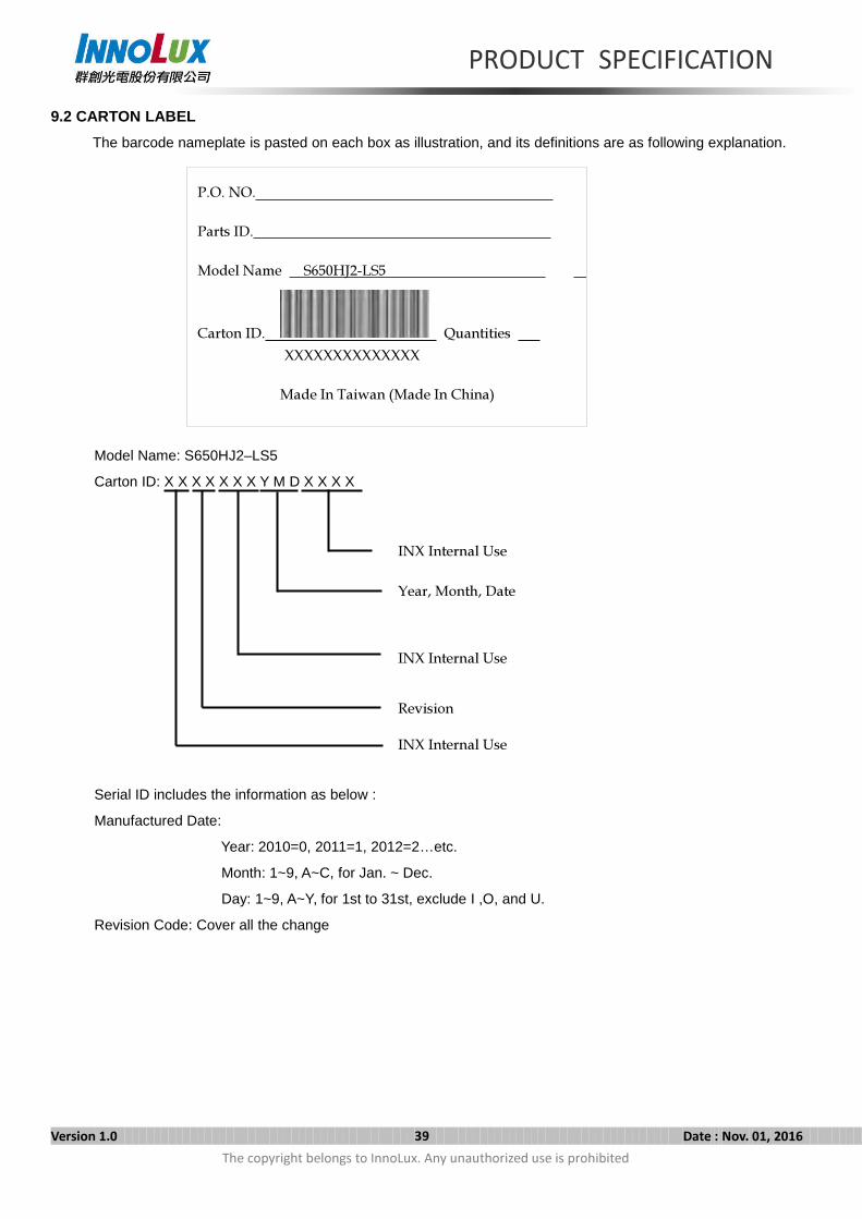
9.2 CARTON LABEL
The barcode nameplate is pasted on each box as illustration, and its definitions are as following explanation.
Model Name: S650HJ2–LS5
Carton ID: X X X X X X X Y M D X X X X
Serial ID includes the information as below :
Manufactured Date:
Year: 2010=0, 2011=1, 2012=2…etc.
Month: 1~9, A~C, for Jan. ~ Dec.
Day: 1~9, A~Y, for 1st to 31st, exclude I ,O, and U.
Revision Code: Cover all the change
P.O. NO.
Parts ID.
Model Name S650HJ2-LS5
Carton ID. QuantitiesXXXXXXXXXXXXXX
Made In Taiwan (Made In China)
INX Internal Use
Year, Month, Date
INX Internal Use
Revision
INX Internal Use
PRODUCT SPECIFICATION
Version 1.0 40 Date : Nov. 01, 2016The copyright belongs to InnoLux. Any unauthorized use is prohibited
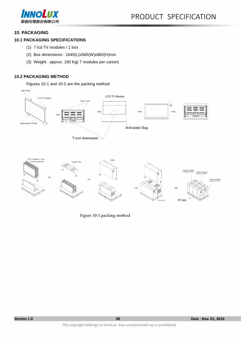
10. PACKAGING
10.1 PACKAGING SPECIFICATIONS
(1) 7 lcd TV modules / 1 box
(2) Box dimensions : 1645(L)x565(W)x982(H)mm
(3) Weight : approx. 190 Kg( 7 modules per carton)
10.2 PACKAGING METHOD
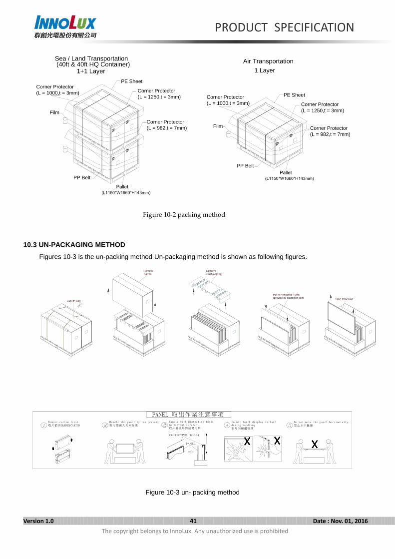
Figures 10-1 and 10-2 are the packing method
PP Belt
Figure 10-1 packing method
PRODUCT SPECIFICATION
Version 1.0 41 Date : Nov. 01, 2016The copyright belongs to InnoLux. Any unauthorized use is prohibited
Sea / Land Transportation
1+1 Layer
Air Transportation
1 Layer
Film
Corner Protector(L = 1000,t = 3mm)
Corner Protector(L = 982,t = 7mm)
PP Belt
Corner Protector(L = 1250,t = 3mm)Film
PE SheetCorner Protector(L = 1000,t = 3mm)
Corner Protector(L = 982,t = 7mm)
PP Belt
Corner Protector(L = 1250,t = 3mm) PE Sheet
(40ft & 40ft HQ Container)
10.3 UN-PACKAGING METHOD
Figures 10-3 is the un-packing method Un-packaging method is shown as following figures.
Remove Carton
Remove Cushion(Top)
Put in Protective Tools(provide by customer-self) Take Panel out
PANEL 取出作業注意事項Handle with protective tools to prevent scratch取片需使用防刮傷治具
Handle the panel by two persons 取片需兩人共同作業
Do not touch display surface during handling取片勿碰觸玻璃
PROTECTIVE TOO LS
PANEL
Remove carton first.取片前須先移除CARTON
Do not move the panel horizontally. 禁止水平搬運
Figure 10-2 packing method
Figure 10-3 un- packing method
PRODUCT SPECIFICATION
Version 1.0 42 Date : Nov. 01, 2016The copyright belongs to InnoLux. Any unauthorized use is prohibited
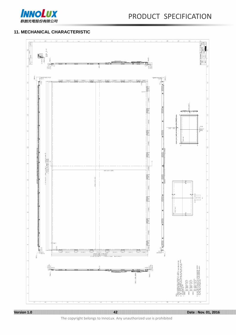
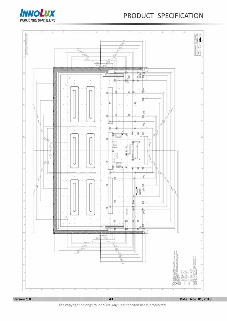
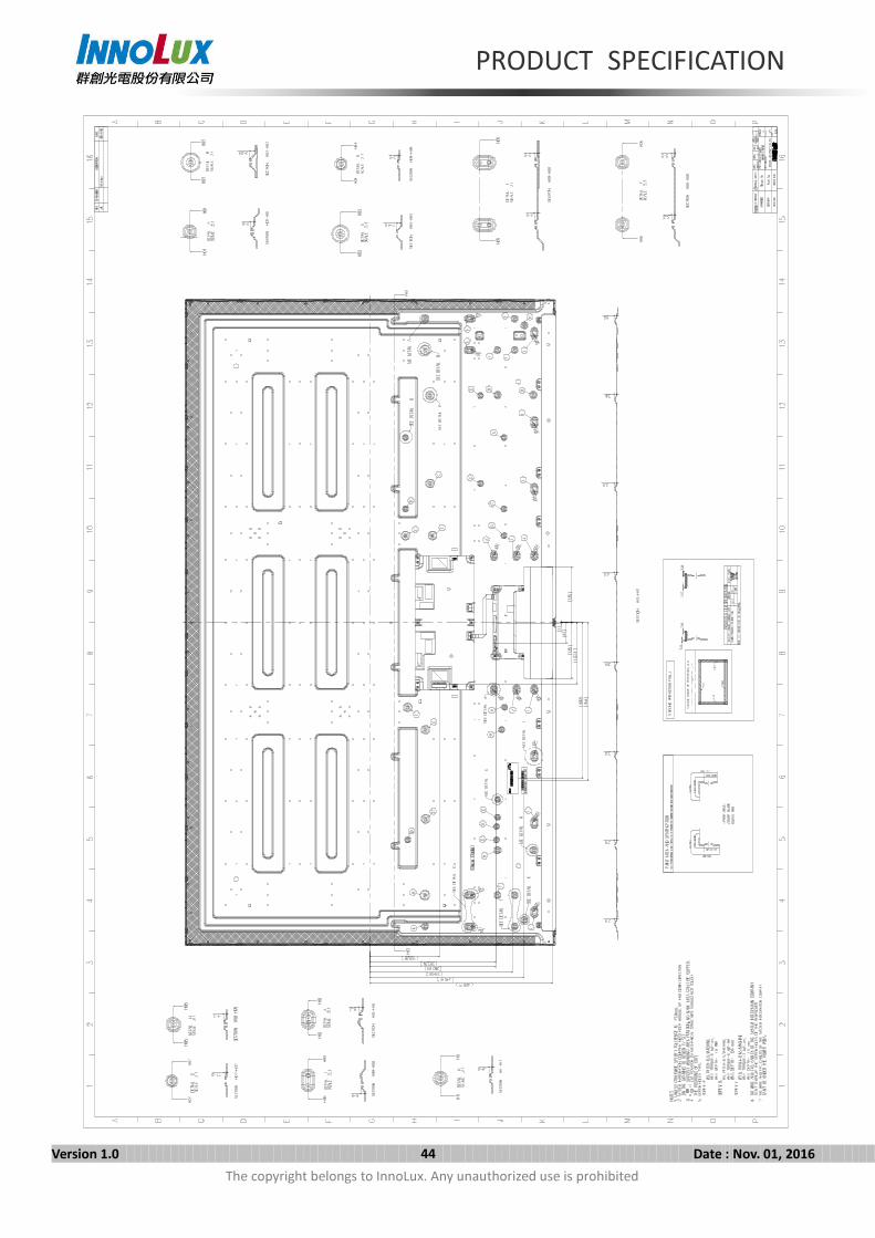
11. MECHANICAL CHARACTERISTIC
PRODUCT SPECIFICATION
Version 1.0 43 Date : Nov. 01, 2016The copyright belongs to InnoLux. Any unauthorized use is prohibited
PRODUCT SPECIFICATION
Version 1.0 44 Date : Nov. 01, 2016The copyright belongs to InnoLux. Any unauthorized use is prohibited
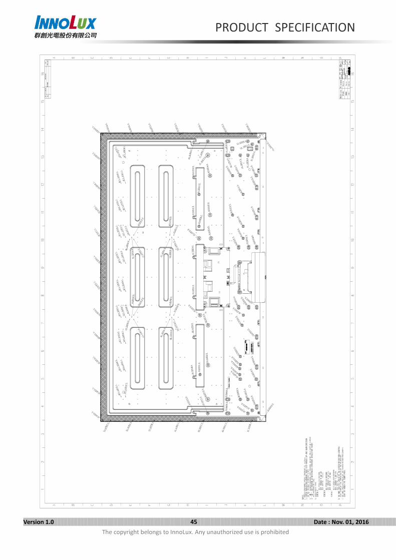
PRODUCT SPECIFICATION
Version 1.0 45 Date : Nov. 01, 2016The copyright belongs to InnoLux. Any unauthorized use is prohibited
PRODUCT SPECIFICATION
Version 1.0 46 Date : Nov. 01, 2016The copyright belongs to InnoLux. Any unauthorized use is prohibited
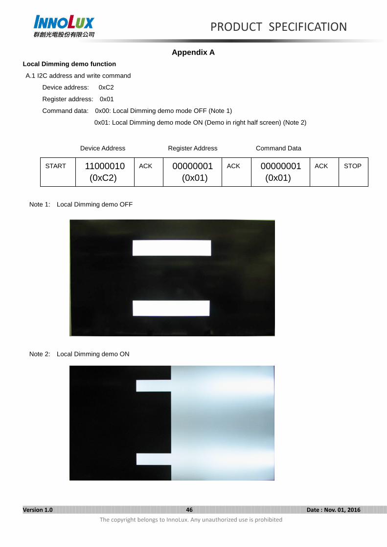
Appendix ALocal Dimming demo function
A.1 I2C address and write command
Device address: 0xC2
Register address: 0x01
Command data: 0x00: Local Dimming demo mode OFF (Note 1)
0x01: Local Dimming demo mode ON (Demo in right half screen) (Note 2)
Note 1: Local Dimming demo OFF
Note 2: Local Dimming demo ON
START 11000010(0xC2)
ACK 00000001(0x01)
ACK 00000001(0x01)
STOP
Device Address Register Address Command Data
ACK
PRODUCT SPECIFICATION
Version 1.0 47 Date : Nov. 01, 2016The copyright belongs to InnoLux. Any unauthorized use is prohibited
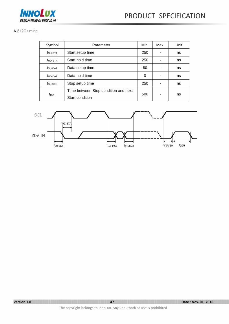
A.2 I2C timing
Symbol Parameter Min. Max. Unit
tSU-STA Start setup time 250 - ns
tHD-STA Start hold time 250 - ns
tSU-DAT Data setup time 80 - ns
tHD-DAT Data hold time 0 - ns
tSU-STO Stop setup time 250 - ns
tBUF
Time between Stop condition and next
Start condition500 - ns

A L L T E C H N O LO G I E S . A L L CO M P E T E N C I E S . O N E S P E C I A L I S T.
w w w . d a t a - m o d u l . c o m
More information and worldwide locations can be found at
DATA MODUL AG
Landsberger Straße 322 DE-80687 Munich Phone: +49-89-56017-0
DATA MODUL WEIKERSHEIM GMBH
Lindenstraße 8 DE-97990 Weikersheim Phone: +49-7934-101-0


![Panel Chimei Innolux v236bj1-Le1 0 [Ds]](https://img.pdfslide.us/doc/110x75/55cf9828550346d03395f0c6/panel-chimei-innolux-v236bj1-le1-0-ds.jpg)