Embed Size (px)
Citation preview

InkjetInkjet PrintingPrinting ForFor MakingMaking FineFineConductorsConductors andand MultiMultiLayerLayer ElectronicsElectronics
Liisa Hakola,Liisa Hakola, ResearchResearch ScientistScientistVTTVTT ––TechnicalTechnical ResearchResearch CentreCentre of Finlandof Finland
e|5:e|5: UV & EBUV & EB TechnologyTechnology ExpoExpo && ConferenceConferenceAprilApril 24th, 200624th, 2006

April 24th, 2006 Liisa Hakola 2
OutlineOutline
1.1. VTTVTT overviewoverview
2.2. InkjetInkjet technologytechnology
3.3. Inkjet forInkjet for makingmaking printedprinted electronicselectronics
4.4. InkjetInkjet printingprinting conductorsconductors
5.5. InkjetInkjet printingprinting multimultilayerlayer electronicselectronics
6.6. SummarySummary

April 24th, 2006 Liisa Hakola 3
VTTVTT ––TechnicalTechnical ResearchResearch CentreCentre of Finlandof Finland
nn Impartial and multidisciplinaryImpartial and multidisciplinaryexpert organisationexpert organisation
nn 2,900 employees2,900 employeesnn Turnover 220 millionTurnover 220 million €€, 5000, 5000
customerscustomersnn Confidential research projects,Confidential research projects,
joint venture projects and strategic,joint venture projects and strategic,selfselffinanced researchfinanced research
STRATEGICRESEARCH
BUSINESSSOLUTIONS
VENTURES
Productiveconsulting services
EXPERTSERVICES
IPR,spinoffs
Newenablingtechnologies
VTTwidesales andmarketing
Research and development

April 24th, 2006 Liisa Hakola 4
DigitalDigital PrintingPrinting ResearchResearch at VTT 1995at VTT 199520072007
PrintableQuality
Indicator
SurfaceProximity
Assay
Sustainpack(EU IP)
1995 1998 2001 2004 2007
Printing ofVariable
Informationon Packages
On Demand Package Printing
Communication in Consumer Packages
ICTApplications
Printable Opticsand Electronics
PRINTO
Functional Inks inInkjet Printing
ManufacturingTechnologies
Based on Inkjet
Dynamic Interactions and ImageQuality in Ink Jet Printing
(EPPProgramme)
Home PrintingFrom Network
Quality Potentialof Digital Photo
Printing
MicroscaleDynamics in
Ink Jet Printing
PublicationsApplications ofHigh Speed IJ
InnovativeDevelopment of
Ink Jet (NI)IntegratingPrinted and
Electronic MediaPRINT ACCESS
MANUFACTURING:
PACKAGING:
PUBLICATION:PRINT
INTERACT
Business fromFunctional
Printing

April 24th, 2006 Liisa Hakola 5
nn StateStateofofthetheartart,, industrialindustrial, piezo, piezo electricelectric inkjetinkjetprintheadsprintheads →→ researchresearch resultsresults upscalableupscalable forforproductionproduction
WaterWater,, oiloil andand solventsolventbasedbased inksinksUVUVcurablecurable inksinksHotHot meltmelt inksinks andand waxeswaxesConductiveConductive andand dielectricdielectric inksinksBiochemicalBiochemical andand diagnosticdiagnostic fluidsfluidsIndicatorIndicator fluidsfluids
InkjetInkjet researchresearch environmentenvironment at VTTat VTT

April 24th, 2006 Liisa Hakola 6
PrintingPrinting methodsmethods
Printing methods
Conventionalprinting
Digitalprinting
Offset
Flexography
Gravure
Screen printing
Electrophotography Inkjet
Dry toner
Liquid toner
Continuous Dropondemand
Binarydeflection
Multipledeflection
Thermal
Piezoelectric
Binary
Greyscale

April 24th, 2006 Liisa Hakola 7
InkjetInkjet printingprinting comparedcompared toto otherother printingprintingtechnologiestechnologies
InkjetInkjetnn CustomisationCustomisation,, smallsmall seriesseriesnn PrintingPrinting speedspeed increasingincreasing ((currentlycurrently
aroundaround 1 m/s)1 m/s)nn SubstrateSubstrate independentindependentnn InkInk developmentdevelopment challengingchallengingnn EasyEasy toto integrateintegrate withwith existingexisting
productionproduction lineslines
ConventionalConventional printingprinting methodsmethodsnn NoNo variablevariable data,data, largelarge volumesvolumesnn MassMass manufacturingmanufacturing withwith highhigh
speedspeed ((aroundaround 20 m/s)20 m/s)nn NotNot allall substratessubstrates suitablesuitablenn InkInk developmentdevelopment notnot soso
challengingchallengingnn IntegrationIntegration requiresrequires spacespace andand
changeschanges inin existingexisting productionproductionlineslines

April 24th, 2006 Liisa Hakola 8
InkjetInkjet printingprinting technologytechnology
nn DigitalDigital nonnonimpactimpact printingprintingmethodmethod, additive, additive
nn SubstrateSubstrate independentindependentnn AccurateAccurate,, highhigh resolutionresolution,, highhigh
speedspeednn PossibilityPossibility forfor massmass customisationcustomisationnn LowLow materialmaterial consumptionconsumptionnn Inks forInks for allall kindskinds ofof applicationsapplications
Drop generator Chargeelectrode
Highvoltagedeflection plate Gutter
Substrate
Continuous inkjet
Orifice
Pressurechamber
Heater
Ink
Dropondemand inkjet

April 24th, 2006 Liisa Hakola 9
BenefitsBenefits of inkjetof inkjet printingprinting inin printedprintedelectronicselectronics
nn DirectDirect writewrite ofof electronicelectronic componentscomponents andand circuitscircuitsnn lessless manufacturingmanufacturing stepsstepsnn lessless materialmaterial wastewastenn costcost savingssavingsnn shortershorter turnaroundturnaround timestimes smallsmall seriesseries andand customisationcustomisation
resistmask + expose
etching
printing materialsubstrateInkjet printing:
substratematerial
spincoating e.g.
Photolithography:
cleaning
April 24th, 2006 Liisa Hakola 10
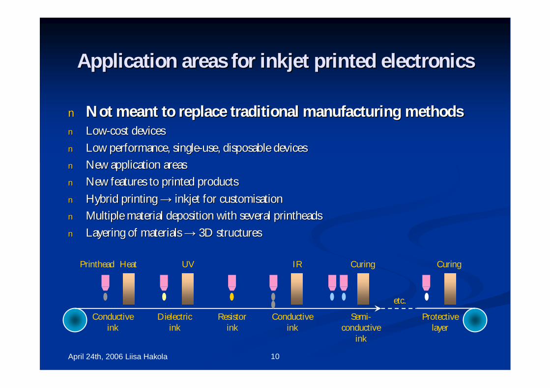
ApplicationApplication areasareas for inkjetfor inkjet printedprinted electronicselectronics
nn NotNot meantmeant toto replacereplace traditionaltraditional manufacturingmanufacturing methodsmethodsnn LowLowcostcost devicesdevicesnn LowLow performanceperformance,, singlesingleuseuse,, disposabledisposable devicesdevicesnn NewNew applicationapplication areasareasnn NewNew featuresfeatures toto printedprinted productsproductsnn HybridHybrid printingprinting inkjet forinkjet for customisationcustomisationnn MultipleMultiple materialmaterial depositiondeposition withwith severalseveral printheadsprintheadsnn LayeringLayering ofof materialsmaterials 3D3D structuresstructures
Conductiveink
HeatPrinthead
Resistorink
Dielectricink
UV
Semiconductive
ink
etc.
Curing
Protectivelayer
Curing
Conductiveink
IR

April 24th, 2006 Liisa Hakola 11
NanoNanoparticleparticle inksinks forfor makingmaking conductorsconductors
nn SmallSmall particleparticle sizesize andand inkink stabilitystabilitycrucialcrucial in inkjetin inkjet printingprinting
nn NanoNanoparticlesparticles provideprovidenn highhigh metalmetal loadingloading withwith lowlow viscosityviscositynn inkink stabilitystabilitynn jettingjetting reliabilityreliabilitynn lowlow curingcuring temperaturetemperature
nn MetalMetal nanonanoparticleparticle inksinks provideprovideprintedprinted conductorsconductors withwith lowlowresistanceresistance valuesvaluesnn eveneven in thein the rangerange ofof µµ
Curing

April 24th, 2006 Liisa Hakola 12
100 µm
50 µmsilvernanoparticleconductorprintedat VTT onpolyimide
InkjetInkjet printingprinting finefine conductorsconductors
nn LinesLines asas finefine asas possiblepossible andandcontinuouscontinuous
nn DropDrop sizesize andand spreadingspreading definedefine linelinewidthwidth
nn PrintPrint resolutionresolution definesdefines linelinecontinuitycontinuity
nn SubstrateSubstrate prepretreatmenttreatment oror preprepatterningpatterning
2.4 mm
2.4 mm

April 24th, 2006 Liisa Hakola 13
InkjetInkjet printingprinting multimultilayerlayer electronicselectronics
nn TransistorsTransistors,, displaysdisplays,, passivepassivecomponentscomponents
nn MultiMulticolourcolour printingprintingnn atat leastleast oneone printhead forprinthead for eacheach inkinknn colorcolor registrationregistration
nn InteractionsInteractions betweenbetween differentdifferentmaterialsmaterialsnn printingprinting onon substratesubstrate vs.vs. printingprinting onon
inkink layerlayernn colourcolour bleedbleed
nn InkInk availabilityavailability
Electrodes
Dielectric
Conductor
Resistor layer
ConductorFerrite layer

April 24th, 2006 Liisa Hakola 14
UVUVcurablecurable dielectricdielectric inkink for inkjetfor inkjet printingprinting
nn PrintingPrinting inin elevatedelevated printheadprintheadtemperaturetemperature
nn DryingDrying withwith absorption and UVabsorption and UVlightlight
nn GoodGood wearwear resistanceresistancenn HighHigh glossglossnn SmoothSmooth inkink layerlayer withoutwithout pinpin
holesholes
1st silverelectrode
2nd silverelectrode
Dielectric inkjet printedbetween electrodes
Example of capacitor
April 24th, 2006 Liisa Hakola 15
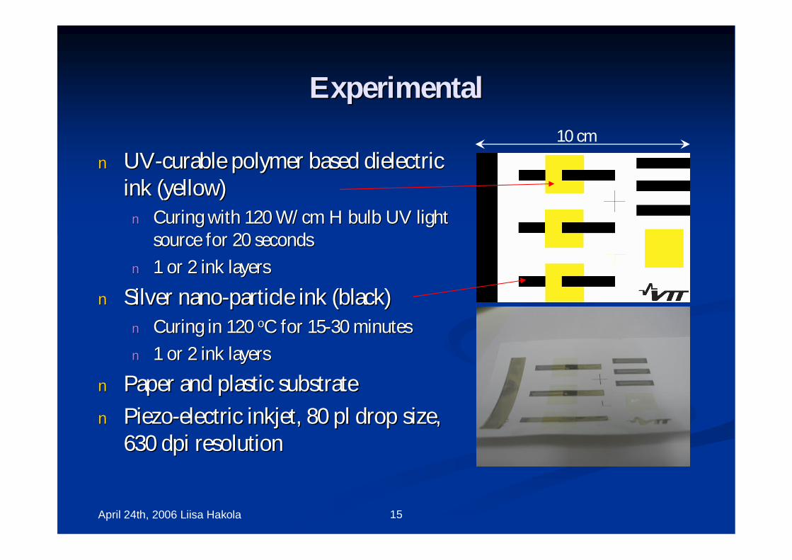
ExperimentalExperimental
nn UVUVcurablecurable polymerpolymer basedbased dielectricdielectricinkink ((yellowyellow))nn CuringCuring withwith 120 W/cm H120 W/cm H bulbbulb UVUV lightlight
sourcesource for 20for 20 secondssecondsnn 11 oror 22 inkink layerslayers
nn SilverSilver nanonanoparticleparticle inkink ((blackblack))nn CuringCuring in 120in 120 ooC for 15C for 153030 minutesminutesnn 11 oror 22 inkink layerslayers
nn PaperPaper andand plasticplastic substratesubstratenn PiezoPiezoelectricelectric inkjet, 80 plinkjet, 80 pl dropdrop sizesize,,
630630 dpidpi resolutionresolution
10 cm

April 24th, 2006 Liisa Hakola 16
0
10
20
30
40
50
60
70
0 200 400 600 800 1000 1200 1400 1600 1800
X (µm)
Z (µm)
10 ink layers, UVcuring 30 s
5 ink layers, UVcuring 30 s
1 ink layer, UVcuring 10 s
1 ink layer, UVcuring 30 s
HeightHeight profileprofile ofof UVUVcuredcured dielectricdielectric inkink layerslayersonon plasticplastic substratesubstrate
peak over scale
~13µm
~20µm
~45µm

April 24th, 2006 Liisa Hakola 17
PerformancePerformance ofof multimultilayerlayer electronicselectronics
600 m 220
1 layer dielectic and 1 layer silver on paper 190 mpin holes?
> 1 M
60190 m
•on paper increase in amount of dielectriclayers increases resistance on top of it
~1 200

April 24th, 2006 Liisa Hakola 18
SummarySummary
nn InkjetInkjet printingprinting suitablesuitable methodmethod forformanufacturingmanufacturing electronicselectronics
nn FineFine inkjetinkjet printedprinted conductorsconductors possiblepossibleeveneven withoutwithout substratesubstrate prepretreatmenttreatment
nn MetalMetal nanonanoparticleparticle inksinks produceproduceconductiveconductive structuresstructures withwith lowlow resistanceresistance
nn InkjetInkjet printingprinting suitablesuitable methodmethod forfor makingmakingmultimultilayerlayer structuresstructures
nn UVUVcurablecurable dielectricdielectric inkink producesproduces smoothsmoothandand thickthick inkink layerslayers

April 24th, 2006 Liisa Hakola 19
ThankThank youyou forfor youryour attentionattention!!
Liisa HakolaLiisa Hakola,, ResearchResearch ScientistScientist
VTTVTT ––TechnicalTechnical ResearchResearch CentreCentre of Finlandof FinlandFunctionalFunctional PrintingPrinting
P.O.BoxP.O.Box 1000, FI1000, FI02044 VTT, Finland02044 VTT, Finland
phonephone: +358 20 722 7206: +358 20 722 7206
faxfax: +358 20 722 7052: +358 20 722 7052
eemailmail:: [email protected]@vtt.fi