Embed Size (px)
Citation preview
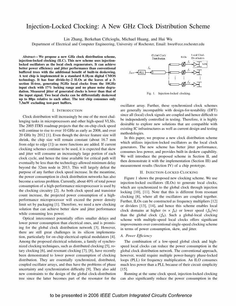
Injection-Locked Clocking: A New GHz Clock Distribution Scheme
Lin Zhang, Berkehan Ciftcioglu, Michael Huang, and Hui WuDepartment of Electrical and Computer Engineering, University of Rochester, Email: [email protected]
Abstract— We propose a new GHz clock distribution scheme,injection-locked clocking (ILC). This new scheme uses injection-locked oscillators as the local clock regenerators. It can achievebetter power efficiency and jitter performance than conventionalbuffered trees with the additional benefit of built-in deskewing.A test chip is implemented in a standard 0.18 � m digital CMOStechnology. It has four divide-by-2 ILOs at the leaves of a 3-section H-tree, generating 5GHz local clocks from the 10GHzinput clock with 17% locking range and no phase noise degra-dation. Measured jitter of generated clocks is lower than that ofthe input signal. Two local clocks can be differentially deskewedup to 80ps relative to each other. The test chip consumes only7.3mW excluding test-port buffers.
I. INTRODUCTION
Clock distribution will increasingly be one of the most chal-lenging tasks in microprocessors and other high-speed VLSIs.The 2005 ITRS roadmap projects that the on-chip clock speedwill continue to rise to over 10 GHz as early as 2008, and over20 GHz by 2012 [1]. Even though the device feature size willshrink, the chip size will remain constant (about 16.7 mmfrom edge to edge [1]) as more functions are added. If currentclocking schemes continue to be used, it is expected that skewand jitter will consume an increasingly large portion of eachclock cycle, and hence the time available for critical path willeventually be less than the technology-allowed minimum delaybeyond the 32nm node in 2013. This will largely defeat thepurpose of any further clock speed increase. In the meantime,the power consumption in clock distribution networks has alsobecome a serious problem. Currently, about 40% of total powerconsumption of a high-performance microprocessor is used bythe clocking circuitry [2]. As both clock speed and transistorcount increase, the projected power consumption of a high-performance microprocessor will exceed the power densitylimit set by packaging [1]. Therefore, we need a new clockingsolution that can achieve better skew and jitter performancewhile consuming less power.
Optical interconnect potentially offers smaller delays andlower power consumption than electrical ones, and is promis-ing for the global clock distribution network [3]. However,there are still great challenges in its silicon implementa-tion, particularly for on-chip electrical-optical modulators [4].Among the proposed electrical solutions, a family of synchro-nized clocking techniques, such as distributed clocking [5], ro-tary clocking [6], and resonant clocking [7], [8], have recentlybeen demonstrated to lower power consumption of clockingdistribution. They are essentially synchronized, distributed,coupled oscillator arrays, and thus have the problems of phaseuncertainty and synchronization difficulty [9]. They also addnew constraints to the design of the global clock-distributiontree since the latter becomes part of the resonator for the
Fig. 1. Injection-locked clocking.
oscillator array. Further, these synchronized clock schemesare generally incompatible with design-for-testability (DFT)since all (local) clock signals are coupled and hence difficult tobe independently controlled in testing. Therefore, it is highlydesirable to explore new solutions that are compatible withexisting IC infrastructures as well as current design and testingmethodologies.
In this paper, we propose a new clock distribution schemewhich utilizes injection-locked oscillators as the local clockgenerators. The new scheme has better jitter performance,consumes less power, and provides built-in deskew capability.We will introduce the proposed scheme in Section II, andthen demonstrate it with the implementation (Section III) andmeasurement results (Section IV) of a chip prototype.
II. INJECTION-LOCKED CLOCKING
Figure 1 shows the proposed new clocking scheme. We useinjection-locked oscillators (ILOs) to generate local clocks,which are synchronized to the global clock through injectionlocking [10], [11]. Note that this is different from resonantclocking [8], where all the oscillators are coupled together.Further, ILOs can be constructed as frequency multipliers [12]or dividers [13], [14], and hence this scheme enables localclock domains at higher ( ������� ) or lower speed ( ���� )than the global clock ( ��� ). Such a global-local clockingscheme with multiple-speed local clocks offers significantimprovements over conventional single-speed clocking schemein terms of power consumption, skew, and jitter.
A. Power Efficiency
The combination of a low-speed global clock and high-speed local clocks can reduce the power consumption in theglobal clock distribution network. The conventional approach,however, would require multiple power-hungry phase-lockedloops (PLL) for frequency multiplication. An ILO consumesmuch less power than a PLL because of their circuit simplicity[15].
Running at the same clock speed, injection-locked clockingcan also significantly reduce the power consumption in the
0 0.05 0.1 0.15 0.2 0.25 0.3 0.3510
0
101
102
Input Amplitude (V)
Vol
tage
Gai
n
InverterILO
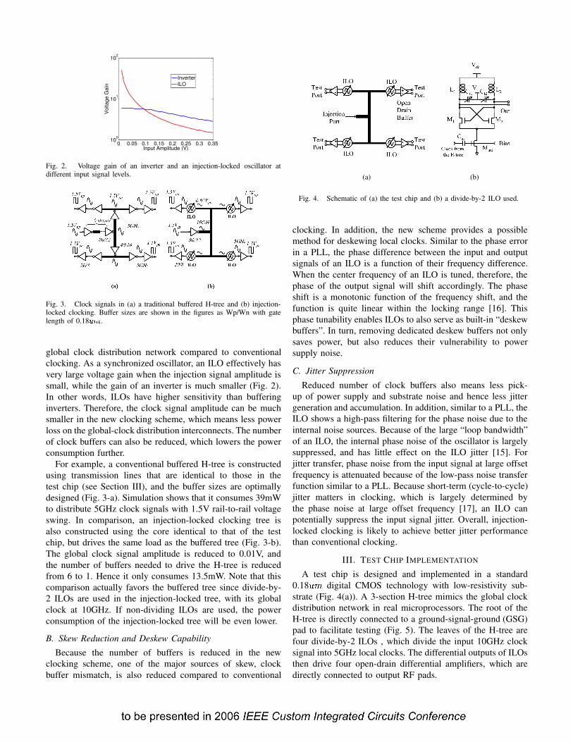
Fig. 2. Voltage gain of an inverter and an injection-locked oscillator atdifferent input signal levels.
Fig. 3. Clock signals in (a) a traditional buffered H-tree and (b) injection-locked clocking. Buffer sizes are shown in the figures as Wp/Wn with gatelength of 0.18 � � .
global clock distribution network compared to conventionalclocking. As a synchronized oscillator, an ILO effectively hasvery large voltage gain when the injection signal amplitude issmall, while the gain of an inverter is much smaller (Fig. 2).In other words, ILOs have higher sensitivity than bufferinginverters. Therefore, the clock signal amplitude can be muchsmaller in the new clocking scheme, which means less powerloss on the global-clock distribution interconnects. The numberof clock buffers can also be reduced, which lowers the powerconsumption further.
For example, a conventional buffered H-tree is constructedusing transmission lines that are identical to those in thetest chip (see Section III), and the buffer sizes are optimallydesigned (Fig. 3-a). Simulation shows that it consumes 39mWto distribute 5GHz clock signals with 1.5V rail-to-rail voltageswing. In comparison, an injection-locked clocking tree isalso constructed using the core identical to that of the testchip, but drives the same load as the buffered tree (Fig. 3-b).The global clock signal amplitude is reduced to 0.01V, andthe number of buffers needed to drive the H-tree is reducedfrom 6 to 1. Hence it only consumes 13.5mW. Note that thiscomparison actually favors the buffered tree since divide-by-2 ILOs are used in the injection-locked tree, with its globalclock at 10GHz. If non-dividing ILOs are used, the powerconsumption of the injection-locked tree will be even lower.
B. Skew Reduction and Deskew Capability
Because the number of buffers is reduced in the newclocking scheme, one of the major sources of skew, clockbuffer mismatch, is also reduced compared to conventional
(a) (b)
Fig. 4. Schematic of (a) the test chip and (b) a divide-by-2 ILO used.
clocking. In addition, the new scheme provides a possiblemethod for deskewing local clocks. Similar to the phase errorin a PLL, the phase difference between the input and outputsignals of an ILO is a function of their frequency difference.When the center frequency of an ILO is tuned, therefore, thephase of the output signal will shift accordingly. The phaseshift is a monotonic function of the frequency shift, and thefunction is quite linear within the locking range [16]. Thisphase tunability enables ILOs to also serve as built-in “deskewbuffers”. In turn, removing dedicated deskew buffers not onlysaves power, but also reduces their vulnerability to powersupply noise.
C. Jitter Suppression
Reduced number of clock buffers also means less pick-up of power supply and substrate noise and hence less jittergeneration and accumulation. In addition, similar to a PLL, theILO shows a high-pass filtering for the phase noise due to theinternal noise sources. Because of the large “loop bandwidth”of an ILO, the internal phase noise of the oscillator is largelysuppressed, and has little effect on the ILO jitter [15]. Forjitter transfer, phase noise from the input signal at large offsetfrequency is attenuated because of the low-pass noise transferfunction similar to a PLL. Because short-term (cycle-to-cycle)jitter matters in clocking, which is largely determined bythe phase noise at large offset frequency [17], an ILO canpotentially suppress the input signal jitter. Overall, injection-locked clocking is likely to achieve better jitter performancethan conventional clocking.
III. TEST CHIP IMPLEMENTATION
A test chip is designed and implemented in a standard0.18 �� digital CMOS technology with low-resistivity sub-strate (Fig. 4(a)). A 3-section H-tree mimics the global clockdistribution network in real microprocessors. The root of theH-tree is directly connected to a ground-signal-ground (GSG)pad to facilitate testing (Fig. 5). The leaves of the H-tree arefour divide-by-2 ILOs , which divide the input 10GHz clocksignal into 5GHz local clocks. The differential outputs of ILOsthen drive four open-drain differential amplifiers, which aredirectly connected to output RF pads.
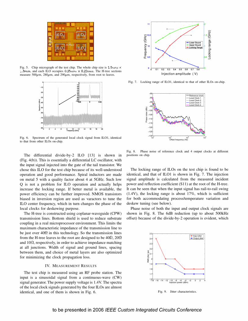
Fig. 5. Chip micrograph of the test chip. The whole chip size is ��� ���������� ����� , and each ILO occupies ��� ������������� ������� . The H-tree sectionsmeasure 500 � m, 280 � m, and 290 � m, respectively, from root to leaves.
Fig. 6. Spectrum of the generated local clock signal from ILO1, identicalto that from other ILOs on-chip.
The differential divide-by-2 ILO [13] is shown in(Fig. 4(b)). This is essentially a differential LC oscillator, withthe input signal injected into the gate of the tail transistor. Wechose this ILO for the test chip because of its well-understoodoperation and good performance. Spiral inductors are madeon metal 5 with a quality factor about 4 at 5GHz. Such lowQ is not a problem for ILO operation and actually helpsincrease the locking range. If better metal is available, thepower efficiency can be further improved. NMOS transistorsbiased in inversion region are used as varactors to tune theILO center frequency, which in turn changes the phase of thelocal clocks for deskewing purpose.
The H-tree is constructed using coplanar-waveguide (CPW)transmission lines. Bottom shield is used to reduce substratecoupling in a real microprocessor environment. This limits themaximum characteristic impedance of the transmission line tobe just over 40 in this technology. So the transmission linesfrom the H-tree leaves to the root are designed to be 40 , 20 and 10 , respectively, in order to achieve impedance matchingat all junctions. Width of signal and ground lines, spacingbetween them, and choice of metal layers are also optimizedfor minimizing the clock propagation loss.
IV. MEASUREMENT RESULTS
The test chip is measured using an RF probe station. Theinput is a sinusoidal signal from a continuous-wave (CW)signal generator. The power supply voltage is 1.4V. The spectraof the local clock signals generated by the four ILOs are almostidentical, and one of them is shown in Fig. 6.
Freq
uenc
y(G
Hz)
Injection amplitude ( V)
Lock
ing
rang
e(G
Hz)
Fig. 7. Locking range of ILO1, identical to that of other ILOs on-chip.
103 104 105 106−130
−125
−120
−115
−110
−105
−100
−95
−90
−85
−80
Offset frequency (Hz)
Pha
se n
oise
(dB
c)
Reference clockLocal Clock 1Local Clock 2Local Clock 3Local Clock 4
Fig. 8. Phase noise of reference clock and 4 output clocks at differentpositions on chip.
The locking range of ILOs on the test chip is found to beidentical, and that of ILO1 is shown in Fig. 7. The injectionsignal amplitude is calculated from the measured incidentpower and reflection coefficient (S11) at the root of the H-tree.It can be seen that when the input signal has rail-to-rail swing(1.4V), the locking range is about 17%, which is sufficientfor both accommodating process/temperature variation anddeskew tuning (see below).
Phase noise of both the input and output clock signals areshown in Fig. 8. The 6dB reduction (up to about 500kHzoffset) because of the divide-by-2 operation is evident, which
−18 −16 −14 −12 −10 −8 −6 −4 −2 0 2 41.6
1.7
1.8
1.9
2
2.1
2.2
2.3
2.4
2.5
Injection power (dBm)
RM
S ji
tter (
ps)
Input jitterOutput jitter
Fig. 9. Jitter characteristics.
0.40.6
0.81
1.2
0.40.60.811.21.4−60
−40
−20
0
20
40
Vtune 2 (V)Vtune 1 (V)
Ske
w (p
s)
zero skewsurface
(a)
−1 −0.8 −0.6 −0.4 −0.2 0 0.2 0.4 0.6 0.8 1−50
−40
−30
−20
−10
0
10
20
30
40
Vdiff (V)
Ske
w (p
s)
(b)
Fig. 10. Deskew capability of ILC. (a) deskewing when tuning ILO1 and/orILO2; (b) deskewing when tuning ILO1 and ILO2 differentially. The skew ismeasured between the two output clock signals of ILO1 and ILO2. Note thatthere is some imbalance between ILO1 and ILO2 caused by mismatch in theclock distribution tree and measurement system.
shows that the internal ILO noise is suppressed by injectionlocking. Fig. 9 shows the long-term RMS jitter of both theinput and output signals measured using a self-referencedjitter measurement method with a sampling oscilloscope [17].The output timing jitter is even less than that of the inputsignal. Considering the frequency division, this result clearlydemonstrates that ILOs can serve as a PLL and clean up theclock signal.
The deskew capability of injection-locked clocking isdemonstrated in Fig. 10. Fig. 10(a) shows the whole deskewsurface when tuning ILO1 by !#"%$&('*) , and/or ILO2 by !+"%$&('-, .One particular tuning example is shown in Fig. 10(b), where!."%$&('*) and !+"%$&('-, are tuned differentially, and the deskewrange is up to 80ps. Because of the large deskew range, smallimbalance in the global clock tree can be easily compensated,which greatly relaxes the requirement on the design and layoutof the clock distribution network.
The test chip consumes a total power of 52.8mW, where45.3mW comes from the 1.8V-supplied open-drain buffers.The ILOs core circuitry working under 1.4V Vdd only con-
sumes 7.3mW when biased low and injection signal is 6dBm.The bias circuitry consumes 0.2mW.
V. CONCLUSION
The proposed injection-locked clocking can significantlyimprove the power efficiency and jitter performance of a GHzclock distribution network. The built-in deskewing capabilityfurther reduces the system complexity and power consump-tion. The benefits will be even greater when this new clockingscheme is applied to future multi-core microprocessors andother high performance system-on-a-chip (SoC) systems be-cause it maintains synchrony between communicating proces-sors.
ACKNOWLEDGMENT
The authors thank Peter Holloway, Bijoy Chatterjee,Jun Wan, Babatunde Akinpelu, Peter Misich, and Carlos Hi-nojosa of National Semiconductor for their support in chipfabrication.
REFERENCES
[1] International technology roadmap of semiconductor. www.itrs.org, 2005.[2] V. Tiwari et al. Reducing Power in High-performance Microprocessors.
In Design Automation Conference (DAC), pages 732–737, 1998.[3] A.V. Mule, E.N. Glytsis, T.K. Gaylord, and J.D. Meindl. Electrical and
Optical Clock Distribution Networks For Gigascale Microprocessors.10(5):582–594, Oct. 2002.
[4] K.C. Cadien et al. Challenges for On-Chip Optical Interconnects. Proc.SPIE, 5730:133–143, Nov. 2005.
[5] V. Gutnik and A.P. Chandrakasan. Active GHz Clock Network UsingDistributed PLLs. IEEE J. Solid-State Circuits, 35(11):1553–1560, Nov.2000.
[6] J. Wood, C. Edwards, and S. Lipa. Rotary Traveling-Wave Oscilla-tor Arrays: a New Clock Technology. IEEE J. Solid-State Circuits,36(11):1654–1665, Nov. 2001.
[7] F. O’Mahony, C.P. Yue, M.A. Horowitz, and S.S. Wong. A 10-GHzGlobal Clock Distribution Using Coupled Standing-Wave Oscillators.IEEE J. Solid-State Circuits, 38(11):1813–1820, Nov. 2003.
[8] S.C. Chang, K.L. Shepard, and P.J. Restle. 1.1 to 1.6GHz DistributedDifferential Oscillator Global Clock Network. In IEEE Int. Solid-StateCircuits Conf. Dig. Tech. Papers, pages 518–519, 2005.
[9] H.-A. Tanaka, A. Hasegawa, H. Mizuno, and T. Endo. Synchroniz-ability of Distributed Clock Oscillators. IEEE Trans. Circuits Syst. I,49(9):1271–1278, Sep. 2002.
[10] R. Adler. A Study of Locking Phenomena in Oscillators. Proc. IRE,34:351–357, June 1946.
[11] K. Kurokawa. Injection Locking of Microwave Solid-State Oscillators.Proc. IEEE, 61(10):1386–1410, Oct. 1973.
[12] K. Kamogawa, T. Tokumitsu, and M. Aikawa. Injection-Locked Oscilla-tor Chain: A Possible Solution to Millimeter-Wave MMIC Synthesizers.IEEE Trans. Microwave Theory Tech., 45(9):1578–1584, Sept. 1997.
[13] H. Rategh and T.H. Lee. Superharmonic Injection-Locked FrequencyDividers. IEEE J. Solid-State Circuits, 34(6):813–821, June 1999.
[14] H. Wu and L. Zhang. A 16-to-18GHz 0.18 � m Epi-CMOS Divide-by-3Injection-Locked Frequency Divider. In IEEE Int. Solid-State CircuitsConf. Dig. Tech. Papers, pages 602–3, 2006.
[15] H. Wu and A. Hajimiri. A 19 GHz, 0.5 mW, 0.35 � m CMOS frequencydivider with shunt-peaking locking-range enhancement. In IEEE Int.Solid-State Circuits Conf. Dig. Tech. Papers, pages 412–3, 2001.
[16] L. Zhang and H. Wu. A Double-Balanced Injection-Locked FrequencyDivider for Tunable Dual-Phase Signal Generation. to appear in 2006IEEE RFIC Symposium, 2006.
[17] A. Hajimiri, S. Limotyrakis, and T.H. Lee. Jitter and Phase Noise of RingOscillators. IEEE J. Solid-State Circuits, 34(6):896–909, June 1999.