Embed Size (px)
Citation preview
Infrared Plasmonics with Conductive Ternary NitridesC. Metaxa,† S. Kassavetis,† J.F. Pierson,‡ D. Gall,§ and P. Patsalas*,†
†Department of Physics, Aristotle University of Thessaloniki, GR-54124 Thessaloniki, Greece‡Institut Jean Lamour (UMR CNRS 7198), Universite de Lorraine, Parc de Saurupt, 54011 Nancy cedex, France§Rensselaer Polytechnic Institute, Department of Materials Science and Engineering, Troy, New York 12180, United States
*S Supporting Information
ABSTRACT: Conductive transition metal nitrides are emerg-ing as promising alternative plasmonic materials that arerefractory and CMOS-compatible. In this work, we show thatternary transition metal nitrides of the B1 structure andconsisting of a combination of group-IVb transition metal, suchas Ti or Zr, and group III (Sc, Y, Al) or group II (Mg, Ca)elements can have tunable plasmonic activity in the infraredrange in contrast to Ta-based ternary nitrides, which exhibitplasmonic performance in the visible and UV ranges. Weconsider the intrinsic quality factors of surface plasmonpolariton for the ternary nitrides, and we calculate thedispersion of surface plasmon polariton and the fieldenhancement at the vicinity of nitride/silica interfaces. Basedon these calculations, it is shown that among these nitrides the most promising are TixSc1−xN and TixMg1−xN. In particular,TixSc1−xN can have plasmonic activity in the usual telecom bands at 850, 1300, and 1550 nm. Still, these nitrides exhibitsubstantial electronic losses mostly due to fine crystalline grains that deteriorate the plasmonic field enhancement. Thisunequivocally calls for improved growth processes that would enable the fabrication of such ternary nitrides of high crystallinity.
KEYWORDS: 1. Surface Plasmon Polariton, 2. Infrared, 3. Conductive Nitrides, 4. Conductor/Dielectric Interfaces
1. INTRODUCTION
The emergence of plasmonics has promised radical break-throughs in various technological sectors, such as micro-electronics,1−4 solar energy harvesting,5−9 photodetection,10−12
optical storage of information,13−16 metamaterials,17−19 andtelecommunications.20−24 The most widely used plasmonicmaterials are gold and silver, which are not compatible withCMOS processing and their plasmonic response is mostly inthe visible spectral range.25,26 The implementation of plasmonictechnology into mainstream telecom applications calls for newplasmonic materials that would be compatible with theestablished Si and fiber optic technology, i.e., materials thatwould have plasmonic response at the 850, 1300, and 1550 nmwavelengths27 and be grown and processed by CMOS-compatible techniques. Conductive transition metal nitrides(TMN), such as TixTa1−xN,
28,29 TixZr1−xN (0 ≤ x ≤ 1),30,31
and TixAl1−xN (0.55<x ≤ 1),32provide a combination of uniqueassets, such as high electron conductivity and mobility,33 highmelting point, and CMOS-compatibility.34 Binary TMNsexhibit strong plasmonic response,35−38 which becomesspectrally tunable for ternary TMNs covering the near UVand the entire visible spectral range.39 Therefore, alloying of thetraditional TMNs, such as TiN, with other elements with twoor three valence electrons might shift their plasmonic responseto the infrared spectral range. This would combine the assets of
plasmonic TMNs with the requirements of the Si telecoms andmight establish plasmonics firmly into the telecom technology.In this work, we demonstrate that TiN-based ternary nitrides
with rare- (Sc, Y) or alkaline-earth (Mg, Ca) elements canestablish a solid platform of conductors whose opticalproperties and plasmonic performance can be spectrally tunablein the infrared spectral range covering at least the 850 and 1300nm wavelengths. In particular, we present experimentaldielectric function spectra of a variety of continuous opaquepolycrystalline films of Ti- or Zr-based TMNs (TixRE1−xN,TixAE1−xN, where RE = Sc, Y and AE = Mg, Ca, and ZrxY1−xN;optical data on the latter were completely missing from theliterature) in the infrared range and we correlate theirfundamental optical parameters with their chemical composi-tion (x). We also report the optical spectra of epitaxialTixSc1−xN(001)/MgO(001), which are found to show superiorplasmonic performance. Finally we complement our study ofthe optical properties of TixAl1−xN by considering itsperformance in the infrared, beyond the range reported in ref32. We evaluate their potential plasmonic performance bycalculating their intrinsic quality factor (QiSPP), the dispersionrelations of Surface Plasmon-Polaritons (SPP) at nitride/silica
Received: December 20, 2016Accepted: March 7, 2017Published: March 7, 2017
Research Article
www.acsami.org
© 2017 American Chemical Society 10825 DOI: 10.1021/acsami.6b16343ACS Appl. Mater. Interfaces 2017, 9, 10825−10834
and nitride/silicon interfaces, and the established field enhance-ment factors (FEF) for SPP.36,40 We show that the mostpromising candidate is the TixSc1−xN system, especially inepitaxial form, which can sustain SPP at interfaces with silicaand silicon at wavelengths compatible with the current telecomtechnology (850, 1300, and 1550 nm). A second candidate,which has poorer performance but consists of more abundantelements, is TixMg1−xN. In both cases, the structural defects ofthe presented samples and their fine grain size, which is mostlydue to the low temperature growth (approximately 300 °C)and secondarily due to the used vacuum arc depositiontechnology,41 reduce their real potential and more effortsshould be dedicated to the improvement of the growth ofhighly crystalline TixSc1−xN and TixMg1−xN on silica andsilicon in order to reduce the electron losses and improve bothQiSPP and FEF.
2. EXPERIMENTAL SECTIONOpaque (thickness >300 nm) polycrystalline TixSc1−xN, TixY1−xN,TixMg1−xN, and TixCa1−xN films were deposited at room temperatureon polished stainless steel substrate using a hybrid reactive arcevaporation−magnetron sputtering process. The Ti vapors werecreated using a cathodic arc source (63 mm diameter and 35 mmthick), while the Sc, Y, Mg, or Ca were sputtered from a magnetroncathode (50 mm diameter and 3 mm thick). The deposition of thefilms was realized in a reactive mixture of argon and nitrogen (40 and70 sccm, respectively; purity 99.999%). A substrate bias voltage of−100 V was applied during the film growth and the arc current appliedto the titanium target was maintained at 90 A, whereas thecomposition x was varying by adjusting the pulsed DC currentapplied to the sputtering target (Advanced Energy Pinnacle+ generatorwith a 50 kHz frequency and an off time of 4 μs); more details onthese experiments are described in ref 41. Opaque (1500 nm thick)ZrxY1−xN films were grown on floating Si substrates by pulse-DC(Advanced Energy Pinnacle+ generator with a 50 kHz frequency andan off time of 4 μs) reactive magnetron sputtering at room
temperature using three individual targets (pure Zr, Zr doped withY 8% or 16%; purity 99.9%) in a mixed Ar/N2 ambient (30/4 sccm,respectively; purity 99.999%) of a working pressure of 0.44 Pa.Opaque (200 nm thick) epitaxial TixSc1−xN films were grown on 10 ×10 × 0.5 mm3 MgO(001) substrates at 750 °C by ultrahigh vacuumreactive magnetron sputter deposition in 99.999% pure N2 dischargesat 0.66 Pa. The Sc to Ti ratio was controlled by the relative powerapplied to two symmetrically positioned magnetrons with 5 cmdiameter Sc (99.9% purity) and Ti (99.999%) targets, respectively, asdescribed in more detail in refs 44 and 45.
The composition x of the films, the [N]/[Metal+RE] or [N]/[Metal+AE] ratios, as well as their crystal structure were studied byenergy dispersive X-rays (EDX), X-ray photoelectron spectroscopy(XPS), and X-ray diffraction (XRD), respectively. EDX were acquiredin a JEOL 840A scanning electron microscope equipped with anOxford Instruments X-ray, analyzer; XPS expereiments were carriedout in a Kratos Axis Ultra DLD instrument equipped with amonochromated Al−Kα beam and a hemispherical sector electronanalyzer, a pass energy of 20 eV was used that provided a broadeningof less than 500 meV for the Ag 3d line; XRD experiments werecarried out in θ-2θ mode using a Bruker (Siemens) D500 apparatuswith Co radiation (λ = 0.179 nm) for Ti-based polycrystalline films,and a Bruker (Siemens) D5000 apparatus with Cu radiation (λ = 0.154nm) for ZrxY1−xN.
The complex dielectric function spectra (ε = ε1+iε2) of the opaquepolycrystalline films were determined by spectroscopic ellipsometry inthe spectral range 0.6−6.5 eV (2067−191 nm) with a step of 50 meVat 70° angle of incidence. Optical transmission and reflection spectraof epitaxial TixSc1−xN were obtained using a Perkin−Elmer Lambda 9spectrophotometer, equipped with integrating sphere for lightcollection, in the spectral range 0.496−6.2 eV (2500−200 nm).Spectral intensity distributions were calibrated using reflection spectrafrom an undoped single-crystal Si(001) wafer; then the dielectricfunction spectra were determined from the optical reflectivityfollowing the procedures described in the Supporting Information.Additionally, spectroscopic data for TixAl1−xN in the infrared range(beyond the range reported in ref 32) are also included in this studyfor comparison purposes.
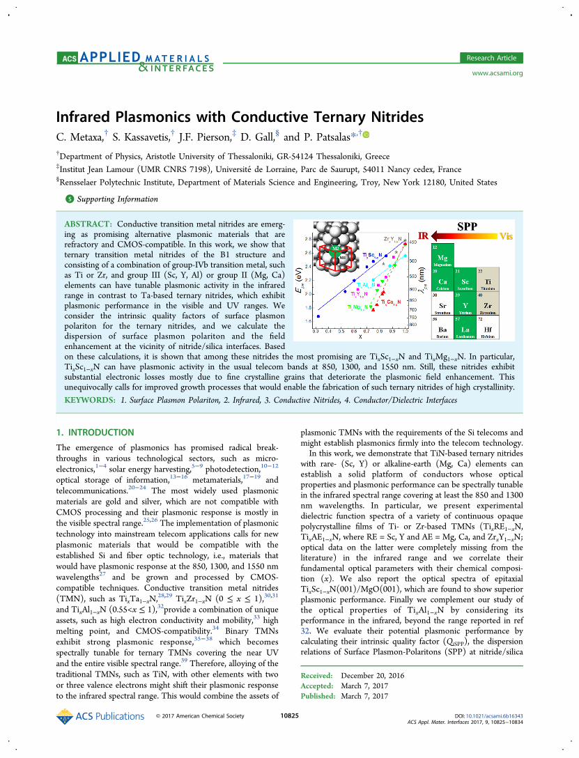
Figure 1. Spectra of the real (ε1) and imaginary (ε2) parts of the dielectric function of opaque films (>300 nm thick) measured in the visible-infraredranges by ellipsometry for (a, b) TixSc1−xN, (c, d) TixY1−xN, and (e, f) ZrxY1−xN.
ACS Applied Materials & Interfaces Research Article
DOI: 10.1021/acsami.6b16343ACS Appl. Mater. Interfaces 2017, 9, 10825−10834
10826
3. RESULTS AND DISCUSSIONTi/Zr and Sc/Y belong to the groups IVb and IIIb of theperiodic table of elements, respectively. As such, they have fouror three valence electrons, respectively, in d and s orbitals.Consequently, their nitrides are conductors and semiconduc-tors, respectively. In particular, the electrical conductivity of allTMNs is due to the excess of d electrons of the metal.28−32 Ti/
Zr and Sc/Y form bonds with nitrogen atoms (valence electronconfiguration 2s22p3) in a stable cubic rocksalt (B1)phase.30,31,41−43 As a result, the ternary TixSc1−xN system isstable over the entire compositional range in the B1structure41,44,45 in contrast to the TixAl1−xN system, whichcan be stabilized in the B1 phase only in a limitedcompositional range.32 Therefore, it is expected that the
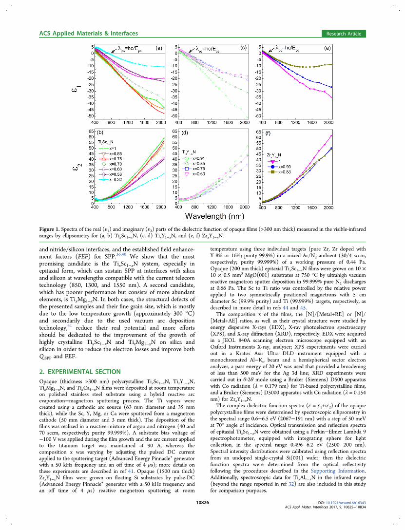
Figure 2. (a) Optical reflectivity spectra of 200 nm thick epitaxial TixSc1−xN films grown on MgO(001) substrates, (b) ε1 spectra of the same films,(c) the variation of the Drude parameters Epu and γD with x for polycrystalline and epitaxial TixSc1−xN.
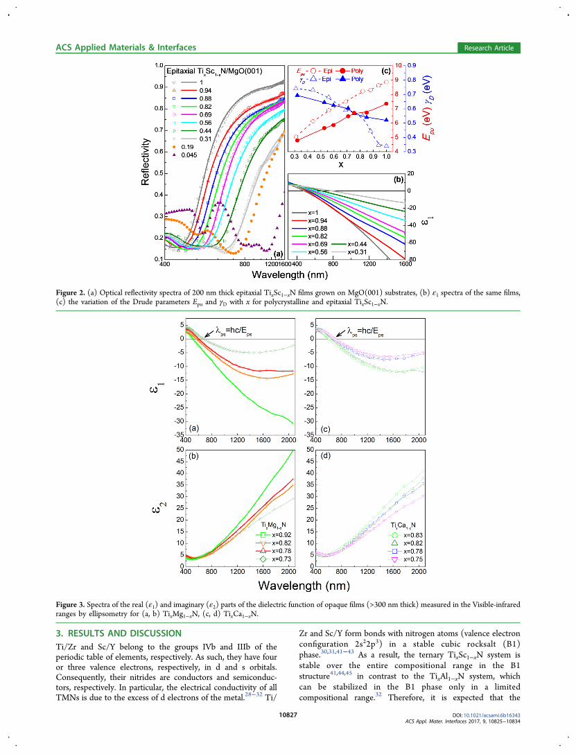
Figure 3. Spectra of the real (ε1) and imaginary (ε2) parts of the dielectric function of opaque films (>300 nm thick) measured in the Visible-infraredranges by ellipsometry for (a, b) TixMg1−xN, (c, d) TixCa1−xN.
ACS Applied Materials & Interfaces Research Article
DOI: 10.1021/acsami.6b16343ACS Appl. Mater. Interfaces 2017, 9, 10825−10834
10827
plasmonic properties of TixSc1−xN films might be extended intothe infrared range, while the plasmonic properties of TixAl1−xNlie in the deep red range.32 TixY1−xN has similar electronconfiguration with TixSc1−xN, but the large lattice mismatchbetween TiN and YN results in TixY1−xN films of lowcrystalline quality, which have high electron losses because ofscattering at the grain boundaries.41 For this reason, in thisstudy, we investigate also the ZrxY1−xN system, which hassimilar electron configuration with TixSc1−xN and TixY1−xN,but smaller mismatch between ZrN and YN.30,41,42 On theother hand, TixAE1−xN (AE = Mg, Ca) are stable in the B1structure in a limited compositional range,41 similar to theTixAl1−xN. However, even relatively small concentrations of Mgor Ca may reduce substantially the carrier density of TiN due totheir two valence electrons.41 So for small concentrations ofMg, or Ca the TixAE1−xN can have conduction electron densitybelow the range that can be achieved by the TixAl1−xN system.Therefore, TixAE1−xN films also have rational perspectives forinfrared plasmonic behavior. The abundance of Mg and Ca, incontrast to the shortage of Sc and Y, is also a significant reasonfor investigating their plasmonic performance.The spectra of the real (ε1) and imaginary (ε2) parts of the
dielectric function of various TMN films in the visible (400−700 nm), near-infrared (700−1400 nm), and in the most of theshort-wavelength-infrared (1400−2067 nm) spectral ranges arepresented in Figures 1 and 2. In particular, Figure 1 shows thedielectric function spectra of ternary compounds of a GroupIIIb (Sc, Y) and a Group IVb (Ti, Zr) element. In order toevaluate the effect of the morphology and crystallographicfeatures to the optical properties in the infrared range of theternary nitrides we also considered the optical reflectivityspectra (Figure 2a) of sputtered, epitaxial TixSc1−xN onMgO(001) substrates. The dielectric function spectra wereextracted from the optical reflectivity as described in theSupporting Information; the relevant ε1 spectra are presentedin Figure 2b and they are characteristic of good conductors withvarying absolute values of ε1 depending on the composition x.Figure 3 shows the dielectric function spectra of ternarycompounds of a Group IIa (Mg, Ca) element and Ti. Similardielectric function spectra for the TixAl1−xN system, but in anarrower spectral range, can be found in ref 39. All the studiedfilms act optically as semi-infinite materials due to theirconductive character and large thickness (>200 nm) with themajor exceptions of the Sc-rich (x = 0.19 and 0.045) epitaxialTixSc1−xN, which exhibit interference fringes indicating theirrelative transparency. Therefore, these samples will not beconsidered in the rest of this study. The ε1 spectra of TMNshave attracted particular attention because they provide a clearqualitative view of their conductive character that rendersnegative ε1 values.
28−30,36−39 In all cases it is evident that theenrichment of TiN or ZrN with a group IIIb (Sc, Y) or a groupIIa (Mg, Ca) element results in less negative ε1 values in theentire infrared range. In the cases of TixMg1−xN and TixCa1−xN(Figure 3a, c) the ε1 values exhibit a broad plateau beyond 1600nm due to excessive electron losses that were quantified in ref41. For short wavelengths, ε1 gets positive values because ofinterband transitions and the accompanying dielectric losses,which are more evident in the ε2 spectra (Figure 1b, d, f, andFigure 3b, d); the dielectric losses, though, are not a source ofconcern in our study because of their spectral separation fromthe infrared range.Of particular practical importance is the screened plasma
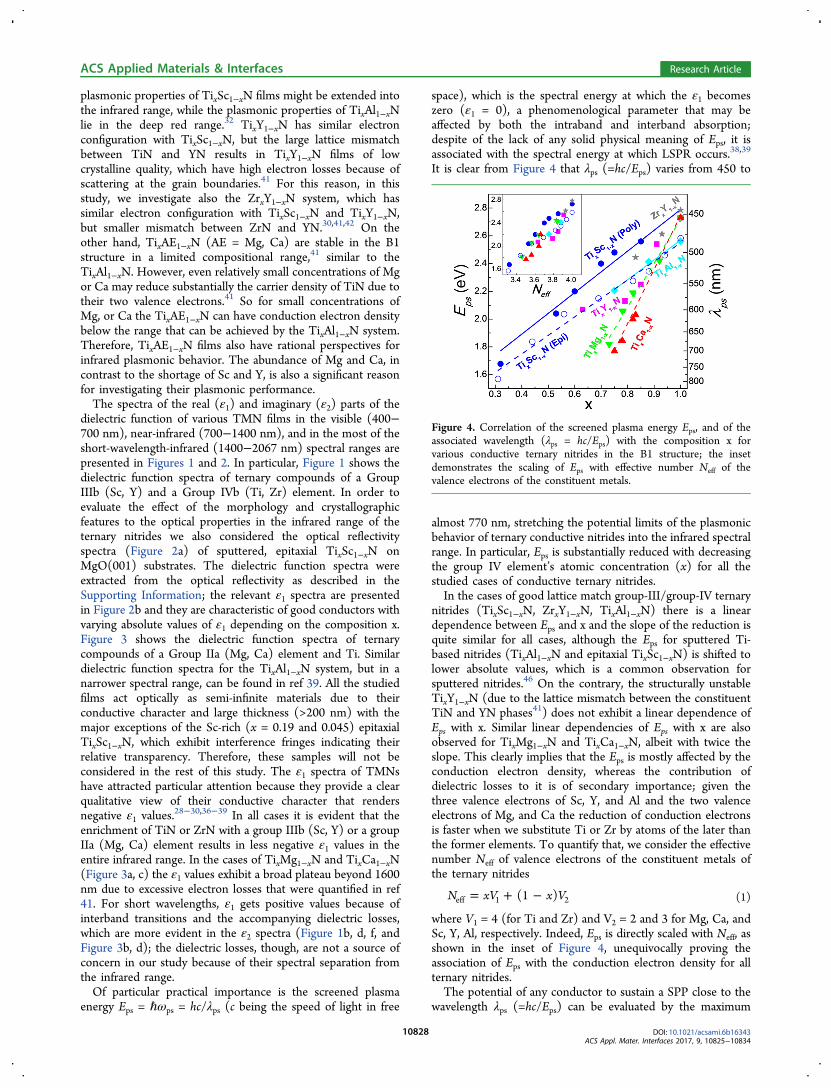
energy Eps = ℏωps = hc/λps (c being the speed of light in free
space), which is the spectral energy at which the ε1 becomeszero (ε1 = 0), a phenomenological parameter that may beaffected by both the intraband and interband absorption;despite of the lack of any solid physical meaning of Eps, it isassociated with the spectral energy at which LSPR occurs.38,39
It is clear from Figure 4 that λps (=hc/Eps) varies from 450 to
almost 770 nm, stretching the potential limits of the plasmonicbehavior of ternary conductive nitrides into the infrared spectralrange. In particular, Eps is substantially reduced with decreasingthe group IV element’s atomic concentration (x) for all thestudied cases of conductive ternary nitrides.In the cases of good lattice match group-III/group-IV ternary
nitrides (TixSc1−xN, ZrxY1−xN, TixAl1−xN) there is a lineardependence between Eps and x and the slope of the reduction isquite similar for all cases, although the Eps for sputtered Ti-based nitrides (TixAl1−xN and epitaxial TixSc1−xN) is shifted tolower absolute values, which is a common observation forsputtered nitrides.46 On the contrary, the structurally unstableTixY1−xN (due to the lattice mismatch between the constituentTiN and YN phases41) does not exhibit a linear dependence ofEps with x. Similar linear dependencies of Eps with x are alsoobserved for TixMg1−xN and TixCa1−xN, albeit with twice theslope. This clearly implies that the Eps is mostly affected by theconduction electron density, whereas the contribution ofdielectric losses to it is of secondary importance; given thethree valence electrons of Sc, Y, and Al and the two valenceelectrons of Mg, and Ca the reduction of conduction electronsis faster when we substitute Ti or Zr by atoms of the later thanthe former elements. To quantify that, we consider the effectivenumber Neff of valence electrons of the constituent metals ofthe ternary nitrides
= + −N xV x V(1 )eff 1 2 (1)
where V1 = 4 (for Ti and Zr) and V2 = 2 and 3 for Mg, Ca, andSc, Y, Al, respectively. Indeed, Eps is directly scaled with Neff, asshown in the inset of Figure 4, unequivocally proving theassociation of Eps with the conduction electron density for allternary nitrides.The potential of any conductor to sustain a SPP close to the
wavelength λps (=hc/Eps) can be evaluated by the maximum
Figure 4. Correlation of the screened plasma energy Eps, and of theassociated wavelength (λps = hc/Eps) with the composition x forvarious conductive ternary nitrides in the B1 structure; the insetdemonstrates the scaling of Eps with effective number Neff of thevalence electrons of the constituent metals.
ACS Applied Materials & Interfaces Research Article
DOI: 10.1021/acsami.6b16343ACS Appl. Mater. Interfaces 2017, 9, 10825−10834
10828
intrinsic quality factor, which is determined by quantitiesassociated with the volume plasmon, and it is defined as47
ω
γ=Q
2iSPPpu2
D2
(2)
where ωpu and γD are the unscreened plasma frequency, i.e. thefrequency of light where a bulk plasmon with energy Epu=ℏωpuoccurs in the conductor, and the Drude broadening factor ofthe conductor, respectively. ωpu and γD are associated with theconduction electron density Ne:
30,32,38,41
ωε
=*
N empue
2
o (3)
where e is the electron charge, εο is the permittivity of freespace and m* is the electron effective mass, in SI units, and withthe conduction electron relaxation time τD:
30,32,38,41
γτ
= 1D
D (4)
respectively, and they can be determined by fitting the dielectricfunction spectra by a Drude-2 Lorentz model, whichdetermines the complex dielectric function ε ω( ) of the materialwith the frequency ω of the incoming light:30,32,38,41
∑ε ω εω
ω γ ω
ω
ω ω γω = −
−+
− +=i
f
i( )
j
j j
j jinf
pu2
2D 1
2o2
o2 2
(5)
In eq 5, εinf is a background constant, larger than unity, which isdue to high-energy contributions (beyond the experimentalspectral range) referring to transitions that are not taken intoaccount by the Lorentz term(s). Each of the Lorentz oscillatorsis describing an interband transition41 and it is located at anenergy position E0j = ℏω0j, with strength f j and damping(broadening) factor γj. Figure 2c summarizes the variations ofEpu and γD for polycrystalline and epitaxial TixSc1−xN forvarious x values, whereas the values for all the samples are listedin the Supporting Information.In an effort to evaluate the intrinsic plasmonic potential of
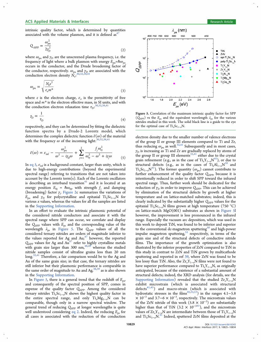
the considered nitride conductors and associate it with thespectral range where SPP can occur, we correlate and displaythe QiSPP values with Eps and the corresponding value of thewavelength λps in Figure 5. The QiSPP values of all theconsidered ternary nitrides are orders of magnitude inferior tothe values reported for Ag and Au;47 however, the reportedQiSPP values for Ag and Au47 refer to highly crystalline metalswith grain size larger than 300 nm,48,49 whereas the studiednitride samples consist of ultrafine grains less than 20 nmlong.32,41 Therefore, a fair comparison would be to the Ag andAu of the same grain size; in that case, the ternary nitrides arestill inferior but their plasmonic performance is comparable inthe same order of magnitude to Au and Ag,38,39 as is also shownin the Supporting Information.In Figure 5, there is a general trend that the redshift of Eps,
and consequently of the spectral position of SPP, comes inexpense of the quality factor QiSPP. Among the consideredternary nitrides TixSc1−xN shows the highest quality factor inthe entire spectral range, and only TixMg1−xN can becomparable, though only in a narrow spectral window. Thegeneral trend of reducing QiSPP at longer wavelengths is quitewell understood considering eq 2. Indeed, the reducing Eps forall cases is associated with the reduction of the conduction
electron density due to the smaller number of valence electronsof the group II or group III elements compared to Ti and Zr,thus reducing ωpu as well.
32,41 Subsequently and in most cases,γD is increasing as Ti and Zr are gradually replaced by atoms ofthe group II or group III elements32,41 either due to the crystalgrain refinement (e.g., as in the case of TixY1−xN
41), or due tostructural defects (e.g., as in the cases of TixAl1−xN
39 andTixSc1−xN
41). The former quantity (ωpu) cannot contribute tofurther enhancement of the quality factor QiSPP, because it isintentionally reduced in order to shift SPP toward the infraredspectral range. Thus, further work should be dedicated for thereduction of γD in order to improve QiSPP. This can be achievedby elimination of the structural defects by growth at highertemperature and on lattice-matched substrates; indeed, this isclearly indicated by the substantially higher QiSPP values for theepitaxial TixSc1−xN films grown at high temperature (750 °C)on lattice-match MgO(001) substrates as shown in Figure 5lhowever, the improvement is less pronounced in the infraredrange. Especially the vacuum arc deposition, which was used inthis work to deposit TiN, was found to be inferior and superiorto the conventional dc-magnetron sputtering50 and high-powerimpulse magnetron sputtering,51 respectively, in terms of thegrain size and of the structural defects of conductive nitridefilms. The importance of the growth optimization is alsoillustrated by the inferior properties of ZrN compared to TiN inthis study in contrast to ZrN and TiN grown by multicathodesputtering and reported in ref 39, where ZrN was found to beless lossy than TiN. Also, the ZrxY1−xN films were not found tohave superior performance compared to TixY1−xN, as originallyanticipated, because of the existence of a substantial amount ofstructural defects; indeed, the XRD analysis (for details, see theSupporting Information) revealed that the studied ZrxY1−xNexhibit microstrain (which is associated with structuraldefects41,45) and macro-strain (which is associated withhydrostatic stresses in the films45,52,53) in the ranges 4.1−5.8× 10⁻³ and 3.7−6 × 10⁻³, respectively. The microstrain valuesof the ZrN nitride of this work (5.8 × 10⁻³) are substantiallyhigher than that of TiN (3.2 × 10−341), and the microstrainvalues of ZrxY1−xN are intermediate between those of TixY1−xNand TixSc1−xN.
41 Indeed, sputtered ZrN films deposited at the
Figure 5. Correlation of the maximum intrinsic quality factor for SPP(QiSPP) vs the Eps and the equivalent wavelength λps for the variousnitrides studied in this work. The solid black line is a guide to the eyefor the optimal case of TixSc1−xN.
ACS Applied Materials & Interfaces Research Article
DOI: 10.1021/acsami.6b16343ACS Appl. Mater. Interfaces 2017, 9, 10825−10834
10829
same growth conditions (pressure, substrate bias, and targetpower) with TiN, exhibited substantially higher compressiveintrinsic stress54 because of the backscattered Ar+ ions from theZr target, the reduced thermalization of Zr atoms in the gasphase and the reduced mobility of Zr adatoms on the activegrowing surface,54,55 all of them due to the higher atomic massof Zr compared to Ti; for all these reasons the growth of pureepitaxial ZrN films was achieved quite recently,56 despite of thegrowth of ZrN films, which include some epitaxial domainssince the late eighties.57 Consequently, ZrN, which is the basisfor ZrxY1−xN, is the source of the structural defects in sputteredZrxY1−xN mostly for kinetic reasons, despite of the lattice matchbetween ZrN and YN.The QiSPP as expressed in eq 2 and as displayed in Figure 5 vs
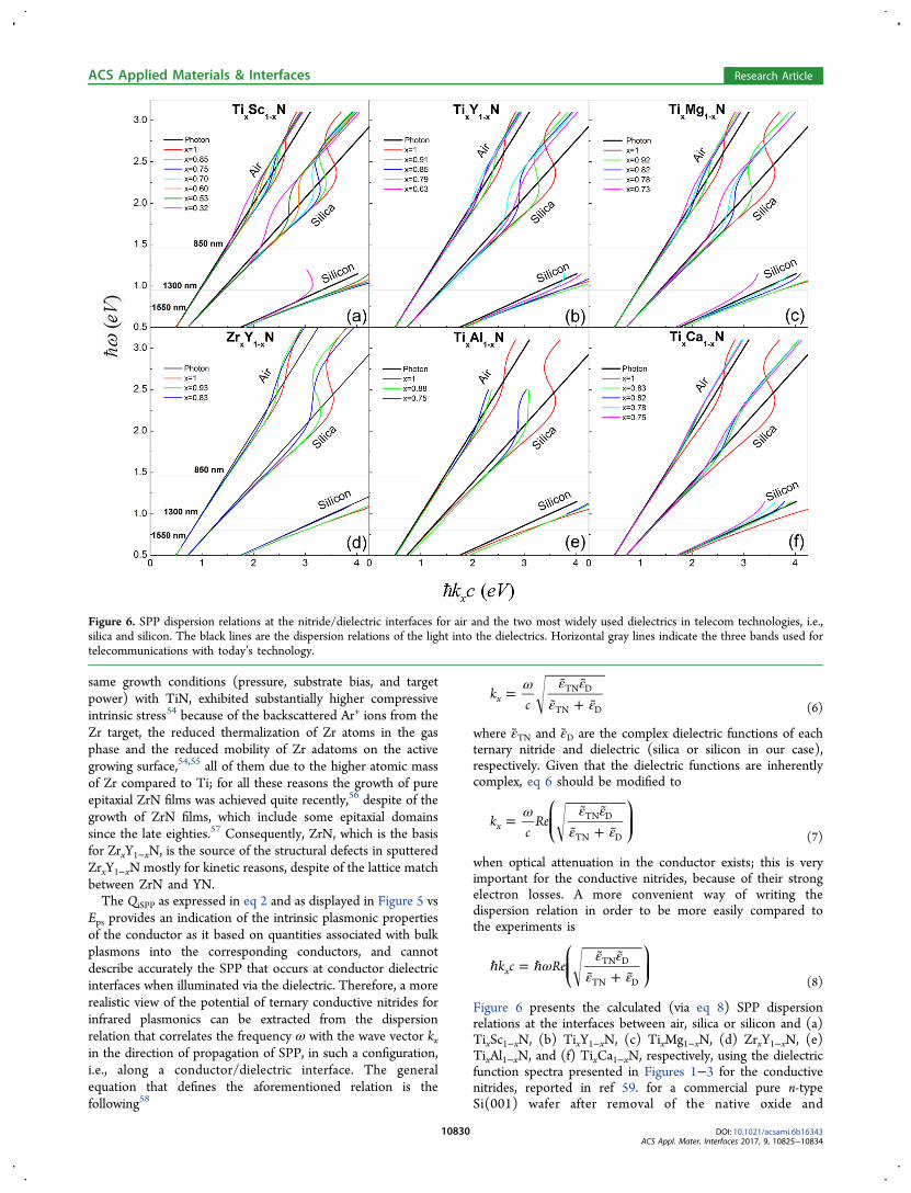
Eps provides an indication of the intrinsic plasmonic propertiesof the conductor as it based on quantities associated with bulkplasmons into the corresponding conductors, and cannotdescribe accurately the SPP that occurs at conductor dielectricinterfaces when illuminated via the dielectric. Therefore, a morerealistic view of the potential of ternary conductive nitrides forinfrared plasmonics can be extracted from the dispersionrelation that correlates the frequency ω with the wave vector kxin the direction of propagation of SPP, in such a configuration,i.e., along a conductor/dielectric interface. The generalequation that defines the aforementioned relation is thefollowing58
ω ε εε ε
=
+ k
cxTN D
TN D (6)
where εTN and εD are the complex dielectric functions of eachternary nitride and dielectric (silica or silicon in our case),respectively. Given that the dielectric functions are inherentlycomplex, eq 6 should be modified to
ω ε εε ε
=
+
⎛⎝⎜⎜
⎞⎠⎟⎟k
cRex
TN D
TN D (7)
when optical attenuation in the conductor exists; this is veryimportant for the conductive nitrides, because of their strongelectron losses. A more convenient way of writing thedispersion relation in order to be more easily compared tothe experiments is
ωε ε
ε εℏ = ℏ
+
⎛⎝⎜⎜
⎞⎠⎟⎟k c Rex
TN D
TN D (8)
Figure 6 presents the calculated (via eq 8) SPP dispersionrelations at the interfaces between air, silica or silicon and (a)TixSc1−xN, (b) TixY1−xN, (c) TixMg1−xN, (d) ZrxY1−xN, (e)TixAl1−xN, and (f) TixCa1−xN, respectively, using the dielectricfunction spectra presented in Figures 1−3 for the conductivenitrides, reported in ref 59. for a commercial pure n-typeSi(001) wafer after removal of the native oxide and
Figure 6. SPP dispersion relations at the nitride/dielectric interfaces for air and the two most widely used dielectrics in telecom technologies, i.e.,silica and silicon. The black lines are the dispersion relations of the light into the dielectrics. Horizontal gray lines indicate the three bands used fortelecommunications with today’s technology.
ACS Applied Materials & Interfaces Research Article
DOI: 10.1021/acsami.6b16343ACS Appl. Mater. Interfaces 2017, 9, 10825−10834
10830
reconstruction of its surface, and reported in ref 60. for silicaglass. Note that the calculation for silicon was performed onlyfor the transparent region, i.e. for photon energies in free spacebelow the band gap of 1.112 eV (wavelength longer than 1115nm), which lies exclusively in the infrared spectral range.The first significant observation is that in all cases the
dispersion relations are characteristic of lossy metals andtherefore involve finite extreme values of kx
58 due toconduction electron (due to finite γD values of all ternarynitrides) and dielectric (due to the existence of interbandtransitions) losses. The consequence of this observation is theexistence of quasi-bound modes at which the slope of thedispersion curve is inversed and the existence of a crossoverenergy at which the SPP dispersion curve crosses the photonline (black lines in all panels of Figure 6).Second, the maximum ℏkxcmax, which defines the SPP point,
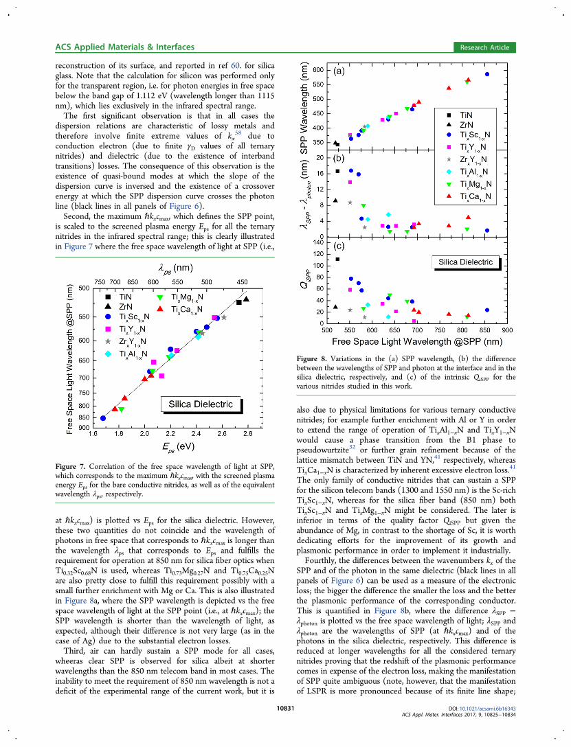
is scaled to the screened plasma energy Eps for all the ternarynitrides in the infrared spectral range; this is clearly illustratedin Figure 7 where the free space wavelength of light at SPP (i.e.,
at ℏkxcmax) is plotted vs Eps for the silica dielectric. However,these two quantities do not coincide and the wavelength ofphotons in free space that corresponds to ℏkxcmax is longer thanthe wavelength λps that corresponds to Eps and fulfills therequirement for operation at 850 nm for silica fiber optics whenTi0.32Sc0.68N is used, whereas Ti0.73Mg0.27N and Ti0.75Ca0.25Nare also pretty close to fulfill this requirement possibly with asmall further enrichment with Mg or Ca. This is also illustratedin Figure 8a, where the SPP wavelength is depicted vs the freespace wavelength of light at the SPP point (i.e., at ℏkxcmax); theSPP wavelength is shorter than the wavelength of light, asexpected, although their difference is not very large (as in thecase of Ag) due to the substantial electron losses.Third, air can hardly sustain a SPP mode for all cases,
wheeras clear SPP is observed for silica albeit at shorterwavelengths than the 850 nm telecom band in most cases. Theinability to meet the requirement of 850 nm wavelength is not adeficit of the experimental range of the current work, but it is
also due to physical limitations for various ternary conductivenitrides; for example further enrichment with Al or Y in orderto extend the range of operation of TixAl1−xN and TixY1−xNwould cause a phase transition from the B1 phase topseudowurtzite32 or further grain refinement because of thelattice mismatch between TiN and YN,41 respectively, whereasTixCa1−xN is characterized by inherent excessive electron loss.41
The only family of conductive nitrides that can sustain a SPPfor the silicon telecom bands (1300 and 1550 nm) is the Sc-richTixSc1−xN, whereas for the silica fiber band (850 nm) bothTixSc1−xN and TixMg1−xN might be considered. The later isinferior in terms of the quality factor QiSPP but given theabundance of Mg, in contrast to the shortage of Sc, it is worthdedicating efforts for the improvement of its growth andplasmonic performance in order to implement it industrially.Fourthly, the differences between the wavenumbers kx of the
SPP and of the photon in the same dielectric (black lines in allpanels of Figure 6) can be used as a measure of the electronicloss; the bigger the difference the smaller the loss and the betterthe plasmonic performance of the corresponding conductor.This is quantified in Figure 8b, where the difference λSPP −λphoton is plotted vs the free space wavelength of light; λSPP andλphoton are the wavelengths of SPP (at ℏkxcmax) and of thephotons in the silica dielectric, respectively. This difference isreduced at longer wavelengths for all the considered ternarynitrides proving that the redshift of the plasmonic performancecomes in expense of the electron loss, making the manifestationof SPP quite ambiguous (note, however, that the manifestationof LSPR is more pronounced because of its finite line shape;
Figure 7. Correlation of the free space wavelength of light at SPP,which corresponds to the maximum ℏkxcmax, with the screened plasmaenergy Eps for the bare conductive nitrides, as well as of the equivalentwavelength λps, respectively.
Figure 8. Variations in the (a) SPP wavelength, (b) the differencebetween the wavelengths of SPP and photon at the interface and in thesilica dielectric, respectively, and (c) of the intrinsic QiSPP for thevarious nitrides studied in this work.
ACS Applied Materials & Interfaces Research Article
DOI: 10.1021/acsami.6b16343ACS Appl. Mater. Interfaces 2017, 9, 10825−10834
10831
indeed, LSPR is clearly observed for the studied nitrides (moredetails are presented in the Supporting Information) thusproving the plasmonic potential of these materials). The samebehavior is also observed for QiSPP vs the free space wavelengthof light (Figure 8c), meaning that the intrinsic characteristics(QiSPP) define to a great extend the extrinsic plasmonicperformance (λSPP−λphoton). Therefore, the considerationsexpressed in the previous paragraphs regarding the improve-ment of QiSPP via improving the growth process of TixSc1−xNand TixMg1−xN would establish a guide toward the improve-ment of infrared plasmonic devices incorporating such nitrides,as well.For most applications the enhancement of the electric field at
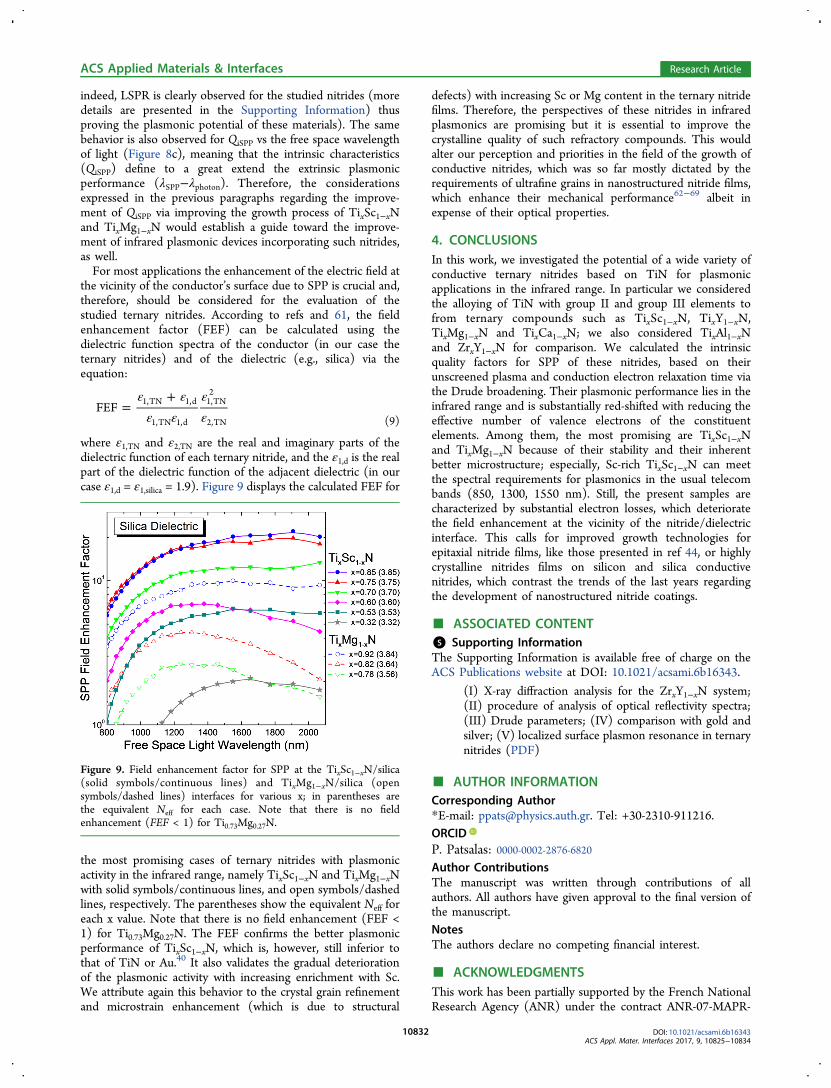
the vicinity of the conductor’s surface due to SPP is crucial and,therefore, should be considered for the evaluation of thestudied ternary nitrides. According to refs and 61, the fieldenhancement factor (FEF) can be calculated using thedielectric function spectra of the conductor (in our case theternary nitrides) and of the dielectric (e.g., silica) via theequation:
ε εε ε
εε
=+
FEF 1,TN 1,d
1,TN 1,d
1,TN2
2,TN (9)
where ε1,TN and ε2,TN are the real and imaginary parts of thedielectric function of each ternary nitride, and the ε1,d is the realpart of the dielectric function of the adjacent dielectric (in ourcase ε1,d = ε1,silica = 1.9). Figure 9 displays the calculated FEF for
the most promising cases of ternary nitrides with plasmonicactivity in the infrared range, namely TixSc1−xN and TixMg1−xNwith solid symbols/continuous lines, and open symbols/dashedlines, respectively. The parentheses show the equivalent Neff foreach x value. Note that there is no field enhancement (FEF <1) for Ti0.73Mg0.27N. The FEF confirms the better plasmonicperformance of TixSc1−xN, which is, however, still inferior tothat of TiN or Au.40 It also validates the gradual deteriorationof the plasmonic activity with increasing enrichment with Sc.We attribute again this behavior to the crystal grain refinementand microstrain enhancement (which is due to structural
defects) with increasing Sc or Mg content in the ternary nitridefilms. Therefore, the perspectives of these nitrides in infraredplasmonics are promising but it is essential to improve thecrystalline quality of such refractory compounds. This wouldalter our perception and priorities in the field of the growth ofconductive nitrides, which was so far mostly dictated by therequirements of ultrafine grains in nanostructured nitride films,which enhance their mechanical performance62−69 albeit inexpense of their optical properties.
4. CONCLUSIONSIn this work, we investigated the potential of a wide variety ofconductive ternary nitrides based on TiN for plasmonicapplications in the infrared range. In particular we consideredthe alloying of TiN with group II and group III elements tofrom ternary compounds such as TixSc1−xN, TixY1−xN,TixMg1−xN and TixCa1−xN; we also considered TixAl1−xNand ZrxY1−xN for comparison. We calculated the intrinsicquality factors for SPP of these nitrides, based on theirunscreened plasma and conduction electron relaxation time viathe Drude broadening. Their plasmonic performance lies in theinfrared range and is substantially red-shifted with reducing theeffective number of valence electrons of the constituentelements. Among them, the most promising are TixSc1−xNand TixMg1−xN because of their stability and their inherentbetter microstructure; especially, Sc-rich TixSc1−xN can meetthe spectral requirements for plasmonics in the usual telecombands (850, 1300, 1550 nm). Still, the present samples arecharacterized by substantial electron losses, which deterioratethe field enhancement at the vicinity of the nitride/dielectricinterface. This calls for improved growth technologies forepitaxial nitride films, like those presented in ref 44, or highlycrystalline nitrides films on silicon and silica conductivenitrides, which contrast the trends of the last years regardingthe development of nanostructured nitride coatings.
■ ASSOCIATED CONTENT*S Supporting InformationThe Supporting Information is available free of charge on theACS Publications website at DOI: 10.1021/acsami.6b16343.
(I) X-ray diffraction analysis for the ZrxY1−xN system;(II) procedure of analysis of optical reflectivity spectra;(III) Drude parameters; (IV) comparison with gold andsilver; (V) localized surface plasmon resonance in ternarynitrides (PDF)
■ AUTHOR INFORMATIONCorresponding Author*E-mail: [email protected]. Tel: +30-2310-911216.ORCIDP. Patsalas: 0000-0002-2876-6820Author ContributionsThe manuscript was written through contributions of allauthors. All authors have given approval to the final version ofthe manuscript.NotesThe authors declare no competing financial interest.
■ ACKNOWLEDGMENTSThis work has been partially supported by the French NationalResearch Agency (ANR) under the contract ANR-07-MAPR-
Figure 9. Field enhancement factor for SPP at the TixSc1−xN/silica(solid symbols/continuous lines) and TixMg1−xN/silica (opensymbols/dashed lines) interfaces for various x; in parentheses arethe equivalent Neff for each case. Note that there is no fieldenhancement (FEF < 1) for Ti0.73Mg0.27N.
ACS Applied Materials & Interfaces Research Article
DOI: 10.1021/acsami.6b16343ACS Appl. Mater. Interfaces 2017, 9, 10825−10834
10832
0007 (COCTAIL) and by the U.S. National ScienceFoundation under Grant 1309490. Dr. D. Pilloud and Dr. A.Hodroj (Institut Jean Lamour) are acknowledged for theircontribution in the nitride thin films deposition. Prof. E.Lidorikis of the University of Ioannina is acknowledged forproviding the analysis software of the optical reflectivity spectra.
■ REFERENCES(1) Dionne, J. A.; Diest, K.; Sweatlock, L. A.; Atwater, H. A.PlasMOStor: A Metal−Oxide−Si Field Effect Plasmonic Modulator.Nano Lett. 2009, 9, 897−902.(2) Wang, L.; Hu, W.; Wang, J.; Wang, X.; Wang, S.; Chen, X.; Lu,W. Plasmon Resonant Excitation in Grating-Gated AlN BarrierTransistors at Terahertz Frequency. Appl. Phys. Lett. 2012, 100,123501.(3) Heeres, R. W.; Kouwenhoven, L. P.; Zwiller, V. QuantumInterference in Plasmonic Circuits. Nat. Nanotechnol. 2013, 8, 719−722.(4) Sheldon, M. T.; van De Groep, J.; Brown, A. M.; Polman, A.;Atwater, H. A. Plasmoelectric Potentials in Metal Nanostructures.Science 2014, 346, 828−831.(5) Atwater, H. A.; Polman, A. Plasmonics for Improved PhotovoltaicDevices. Nat. Mater. 2010, 9, 205−213.(6) Aubry, A.; Lei, D. Y.; Fernandez-Dominguez, A. I.; Sonnefraud,Y.; Maier, S. A.; Pendry, J. B. Plasmonic Light-Harvesting Devices overthe Whole Visible Spectrum. Nano Lett. 2010, 10, 2574−2579.(7) Gan, Q.; Bartoli, F. J.; Kafafi, Z. H. Plasmonic-Enhanced OrganicPhotovoltaics: Breaking the 10% Efficiency Barrier. Adv. Mater. 2013,25, 2385−2396.(8) Beliatis, M. J.; Henley, S. J.; Han, S.; Gandhi, K.; Adikaari, D.;Stratakis, E.; Kymakis, E.; Silva, S. R. P. Organic Solar Cells withPlasmonic Layers Formed by Laser Nanofabrication. Phys. Chem.Chem. Phys. 2013, 15, 8237−8244.(9) White, T. P.; Catchpole, K. R. Plasmon-Enhanced InternalPhotoemission for Photovoltaics: Theoretical Efficiency Limits. Appl.Phys. Lett. 2012, 101, 073905.(10) Sobhani, A.; Knight, M. W.; Wang, Y.; Zheng, B.; King, N. S.;Brown, L. V.; Fang, Z.; Nordlander, P.; Halas, N. J. NarrowbandPhotodetection in the Near-Infrared with a Plasmon-Induced HotElectron Device. Nat. Commun. 2013, 4, 1643.(11) Konstantatos, G.; Sargent, E. H. Nanostructured Materials forPhoton Detection. Nat. Nanotechnol. 2010, 5, 391−400.(12) Chalabi, H.; Schoen, D.; Brongersma, M. L. Hot-ElectronPhotodetection with a Plasmonic Nanostripe Antenna. Nano Lett.2014, 14, 1374−1380.(13) Montelongo, Y.; Tenorio-Pearl, J. O.; Williams, C.; Zhang, S.;Milne, W. I.; Wilkinson, T. D. Plasmonic Nanoparticle Scattering forColor Holograms. Proc. Natl. Acad. Sci. U. S. A. 2014, 111, 12679−12683.(14) Siozios, A.; Koutsogeorgis, D. C.; Lidorikis, E.; Dimitrakopulos,G. P.; Kehagias, T.; Zoubos, H.; Komninou, P.; Cranton, W. M.;Kosmidis, C.; Patsalas, P. Optical Encoding by Plasmon-BasedPatterning: Hard and Inorganic Materials Become Photosensitive.Nano Lett. 2012, 12, 259−263.(15) Zijlstra, P.; Chon, J. W. M.; Gu, M. Five-Dimensional OpticalRecording Mediated by Surface Plasmons in Gold Nanorods. Nature2009, 459, 410−413.(16) Kumar, K.; Duan, H.; Hegde, R. S.; Koh, S. C. W.; Wei, J. N.;Yang, J. K. W. Printing Colour at the Optical Diffraction Limit. Nat.Nanotechnol. 2012, 7, 557−561.(17) Pendry, J. B.; Martin-Moreno, L.; Garcia-Vidal, F. J. MimickingSurface Plasmons with Structured Surfaces. Science 2004, 305, 847−848.(18) Boltasseva, A. Empowering Plasmonics and MetamaterialsTechnology with New Material Platforms. MRS Bull. 2014, 39, 461−468.
(19) Boltasseva, A.; Shalaev, V. M. Fabrication of Optical Negative-Index Metamaterials: Recent Advances and Outlook. Metamaterials2008, 2, 1−17.(20) Sandtke, M.; Kuipers, L. Slow Guided Surface Plasmons atTelecom Frequencies. Nat. Photonics 2007, 1, 573−576.(21) Burgos, S. P.; Lee, H. W.; Feigenbaum, E.; Briggs, R. M.;Atwater, H. A. Synthesis and Characterization of Plasmonic ResonantGuided Wave Networks. Nano Lett. 2014, 14, 3284−3292.(22) Shin, W.; Cai, W.; Catrysse, P. B.; Veronis, G.; Brongersma, M.L.; Fan, S. Broadband Sharp 90-Degree Bends and T-splitters inPlasmonic Coaxial Waveguides. Nano Lett. 2013, 13, 4753−4758.(23) Li, X.; Jiang, T.; Shen, L.; Deng, X. Subwavelength Guiding ofChannel Plasmon Polaritons by Textured Metallic Grooves atTelecom Wavelengths. Appl. Phys. Lett. 2013, 102, 031606.(24) Holmgaard, T.; Bozhevolnyi, S. I.; Markey, L.; Dereux, A.;Krasavin, A. V.; Bolger, P.; Zayats, A. V. Efficient Excitation ofDielectric-Loaded Surface Plasmon-Polariton Waveguide Modes atTelecommunication Wavelengths. Phys. Rev. B: Condens. Matter Mater.Phys. 2008, 78, No. 165431, DOI: 10.1103/PhysRevB.78.165431.(25) Lenci, S.; De Jaeger, B.; Carbonell, L.; Hu, J.; Mannaert, G.;Wellekens, D.; You, S.; Bakeroot, B.; Decoutere, S. Au-free AlGaN/GaN Power Diode on 8-in Si Substrate with Gated Edge Termination.IEEE Electron Device Lett. 2013, 34, 1035−1037.(26) Babicheva, V. E.; Kinsey, N.; Naik, G. V.; Ferrera, M.;Lavrinenko, A. V.; Shalaev, V. M.; Boltasseva, A. Towards CMOS-Compatible Nanophotonics: Ultra-Compact Modulators UsingAlternative Plasmonic Materials. Opt. Express 2013, 21, 27326−27337.(27) Nick, M. Fiber Optic Telecommunication (Module 1.8). InFundamentals of Photonics; Roychoudhuri, C., Ed.; SPIE (InternationalSociety for Optics and Photonics): Bellingham, WA, 2000; pp298.(28) Matenoglou, G. M.; Lekka, Ch.E.; Koutsokeras, L. E.; Karras, G.;Kosmidis, C.; Evangelakis, G. A.; Patsalas, P. Structure and ElectronicProperties of Conducting, Ternary TixTa1−xN films. J. Appl. Phys.2009, 105, 103714.(29) Koutsokeras, L. E.; Abadias, G.; Lekka, Ch.E.; Matenoglou, G.M.; Anagnostopoulos, D. F.; Evangelakis, G. A.; Patsalas, P.Conducting Transition Metal Nitride Thin Films With Tailored CellSizes: The Case of δ- TixTa1‑xN. Appl. Phys. Lett. 2008, 93, 011904.(30) Matenoglou, G. M.; Koutsokeras, L. E.; Patsalas, P. PlasmaEnergy and Work Function of Conducting Transition Metal Nitridesfor Electronic Applications. Appl. Phys. Lett. 2009, 94, 152108.(31) Matenoglou, G. M.; Koutsokeras, L. E.; Lekka, Ch.E.; Abadias,G.; Kosmidis, C.; Evangelakis, G. A.; Patsalas, P. Structure, Stabilityand Bonding of Ternary Transition Metal Nitrides. Surf. Coat. Technol.2009, 204, 911−914.(32) Kassavetis, S.; Abadias, G.; Vourlias, G.; Bantsis, G.;Logothetidis, S.; Patsalas, P. Optical Properties of TixAl1‑xN ThinFilms in the Whole Compositional range. Surf. Coat. Technol. 2016,295, 125−129.(33) Evangelou, E. K.; Konofaos, N.; Aslanoglou, X. A.; Dimitriadis,C. A.; Patsalas, P.; Logothetidis, S.; Kokkoris, M.; Kossionides, E.;Vlastou, R.; Groetschel, R. Characterization of Magnetron SputteringDeposited Thin Films of TiN for Use as a Metal Electrode on TiN/SiO2/Si Metal−Oxide−Semiconductor Devices. J. Appl. Phys. 2000,88, 7192−7196.(34) Dimitriadis, C. A.; Lee, J. I.; Patsalas, P.; Logothetidis, S.; Tassis,D. H.; Brini, J.; Kamarinos, G. Characteristics of TiNx/n-Si SchottkyDiodes Deposited by Reactive Magnetron Sputtering. J. Appl. Phys.1999, 85, 4238−4242.(35) Cortie, M. B.; Giddings, J.; Dowd, A. Optical Properties andPlasmon Resonances of Titanium Nitride Nanostructures. Nano-technology 2010, 21, 2010.(36) Naik, G. V.; Shalaev, V. M.; Boltasseva, A. Alternative PlasmonicMaterials: Beyond Gold and Silver. Adv. Mater. 2013, 25, 3264−3294.(37) Naik, G. V.; Saha, B.; Liu, J.; Saber, S. M.; Stach, E. A.;Irudayaraj, J. M. K.; Sands, T. D.; Shalaev, V. M.; Boltasseva, A.Epitaxial Superlattices with Titanium Nitride as a PlasmonicComponent for Optical Hyperbolic Metamaterials. Proc. Natl. Acad.Sci. U. S. A. 2014, 111, 7546−7551.
ACS Applied Materials & Interfaces Research Article
DOI: 10.1021/acsami.6b16343ACS Appl. Mater. Interfaces 2017, 9, 10825−10834
10833
(38) Patsalas, P.; Kalfagiannis, N.; Kassavetis, S. Optical Propertiesand Plasmonic Performance of Titanium Nitride. Materials 2015, 8,3128−3154.(39) Kassavetis, S.; Bellas, D.; Abadias, G.; Lidorikis, E.; Patsalas, P.Plasmonic Spectral Tunability of Conductive Ternary Nitrides. Appl.Phys. Lett. 2016, 108, 263110.(40) West, P. R.; Ishii, S.; Naik, G. V.; Emani, N. K.; Shalaev, V. M.;Boltasseva, A. Searching for Better Plasmonic Materials. Laser Phot.Rev. 2010, 4, 795−808.(41) Kassavetis, S.; Hodroj, A.; Metaxa, C.; Logothetidis, S.; Pierson,J. F.; Patsalas, P. Optical and Electronic Properties of ConductiveTernary Nitrides with Rare- or Alkaline-Earth Elements. J. Appl. Phys.2016, 120, 225106.(42) Stampfl, C.; Mannstadt, W.; Asahi, R.; Freeman, A. J. ElectronicStructure and Physical Properties of Early Transition MetalMononitrides: Density-Functional Theory LDA, GGA, andScreened-Exchange LDA FLAPW Calculations. Phys. Rev. B: Condens.Matter Mater. Phys. 2001, 63, 155106.(43) Gregoire, J. M.; Kirby, S. D.; Turk, M. E.; van Dover, R. B.Structural, Electronic and Optical Properties of (Sc,Y)N SolidSolutions. Thin Solid Films 2009, 517, 1607−1609.(44) Gall, D.; Petrov, I.; Greene, J. E. Epitaxial Sc1‑xTixN(001):Optical and Electronic Transport Properties. J. Appl. Phys. 2001, 89,401−409.(45) Gall, D.; Stoehr, M.; Greene, J. E. Vibrational Modes in EpitaxialSc1−xTixN(001) Layers: An Ab-Initio Calculation and RamanSpectroscopy Study. Phys. Rev. B: Condens. Matter Mater. Phys. 2001,64174302, art. no. 174302.10.1103/PhysRevB.64.174302(46) Koutsokeras, L. E.; Abadias, G.; Patsalas, P. Texture andMicrostructure Evolution in Single-Phase TixTa1−xN Alloys of RocksaltStructure. J. Appl. Phys. 2011, 110, 043535.(47) Blaber, M. G.; Arnold, M. D.; Ford, M. J. A review of the OpticalProperties of Alloys and Intermetallics for Plasmonics. J. Phys.:Condens. Matter 2010, 22, 143201.(48) Johnson, P. B.; Christy, R. W. Optical Constants of the NobleMetals. Phys. Rev. B 1972, 6, 4370−4379.(49) Adamov, M.; Perovic, B.; Nenadovic, T. Electrical and StructuralProperties of Thin Gold Films Obtained by Vacuum Evaporation andSputtering. Thin Solid Films 1974, 24, 89−100.(50) Gautier, C.; Moussaoui, H.; Elstner, F.; Machet, J. ComparativeStudy of Mechanical and Structural Properties of CrN FilmsDeposited by D.C. Magnetron Sputtering and Vacuum ArcEvaporation. Surf. Coat. Technol. 1996, 86−87, 254−262.(51) Purandare, Y.; Ehiasarian, A.; Santana, A.; Hovsepian, P. ZrNCoatings Deposited by High Power Impulse Magnetron Sputteringand Cathodic Arc Techniques. J. Vac. Sci. Technol., A 2014, 32, 031507.(52) Abadias, G. Stress and Preferred Orientation in Nitride-BasedPVD Coatings. Surf. Coat. Technol. 2008, 202, 2223−2235.(53) Patsalas, P.; Gravalidis, C.; Logothetidis, S. Surface Kinetics andSubplantation Phenomena Affecting the Texture, Morphology, Stress,and Growth Evolution of Titanium Nitride Films. J. Appl. Phys. 2004,96, 6234−6246.(54) Abadias, G.; Koutsokeras, L. E.; Guerin, Ph.; Patsalas, P. StressEvolution in Magnetron Sputtered Ti−Zr−N and Ti−Ta−N FilmsStudied by In-Situ Wafer Curvature: Role of Energetic Particles. ThinSolid Films 2009, 518, 1532−1537.(55) Koutsokeras, L. E.; Abadias, G. Intrinsic Stress in ZrN ThinFilms: Evaluation of Grain Boundary Contribution from In-Situ WaferCurvature and Ex-Situ X-Ray Diffraction Techniques. J. Appl. Phys.2012, 111, 093509.(56) Mei, A. B.; Howe, B. M.; Zhang, C.; Sardela, M.; Eckstein, J. N.;Hultman, L.; Rockett, A.; Petrov, I.; Greene, J. E. Physical Propertiesof Epitaxial ZrN/MgO(001) Layers Grown by Reactive MagnetronSputtering. J. Vac. Sci. Technol., A 2013, 31, 061516.(57) Barnett, S. A.; Hultman, L.; Sundgren, J.-E.; Ronin, F.; Rohde, S.Epitaxial Growth of ZrN on Si(100). Appl. Phys. Lett. 1988, 53, 400−403.(58) Maier, S. A. Plasmonics: Fundamentals and Applications; SpringerScience and Business: New York, 2007; pp 65−87.
(59) Patsalas, P.; Logothetidis, S. Interface Properties and StructuralEvolution of TiN/Si and TiN/GaN Heterostructures. J. Appl. Phys.2003, 93, 989−998.(60) Malitson, I. H. Interspecimen Comparison of the RefractiveIndex of Fused Silica. J. Opt. Soc. Am. 1965, 55, 1205−1208.(61) Shalaev, V. M. Fractal Nano-Composites: Giant Local-FieldEnhancement of Optical Responses. AIP Conf. Proc. 2000, 560, 237−258.(62) Veprek, S. The Search for Novel, Superhard Materials. J. Vac.Sci. Technol., A 1999, 17, 2401−2420.(63) Musil, J. Hard and Superhard Nanocomposite Coatings. Surf.Coat. Technol. 2000, 125, 322−330.(64) Sproul, W. D. New Routes in the Preparation of MechanicallyHard Films. Science 1996, 273, 889−892.(65) Musil, J.; Hruby, H. Superhard Nanocomposite Ti1‑xAlxN FilmsPrepared by Magnetron Sputtering. Thin Solid Films 2000, 365, 104−109.(66) Patscheider, J. Nanocomposite Hard Coatings for WearProtection. MRS Bull. 2003, 28, 180−183.(67) Sproul, W. D. Physical Vapor Deposition Tool Coatings. Surf.Coat. Technol. 1996, 81, 1−7.(68) Mayrhofer, P. H.; Mitterer, C.; Hultman, L.; Clemens, H.Microstructural Design of Hard Coatings. Prog. Mater. Sci. 2006, 51,1032−1114.(69) Mayrhofer, P. H.; Horling, A.; Karlsson, L.; Sjolen, J.; Larsson,T.; Mitterer, C.; Hultman, L. Self-Organized Nanostructures in the Ti-Al-N system. Appl. Phys. Lett. 2003, 83, 2049−2051.
ACS Applied Materials & Interfaces Research Article
DOI: 10.1021/acsami.6b16343ACS Appl. Mater. Interfaces 2017, 9, 10825−10834
10834


![INVITED PAPER QuantumPlasmonics€¦ · ters near plasmonic structures [20], graphene plasmonics [21], semiconductor plasmonics [22], hot electrons [23], and active quantum plasmonics](https://img.pdfslide.us/doc/110x75/5f0859367e708231d4219104/invited-paper-quantumplasmonics-ters-near-plasmonic-structures-20-graphene-plasmonics.jpg)