Embed Size (px)
Citation preview
PROCEEDINGS OF THE
FIRST INTERNATIONAL CONFERENCE ON
SCIENCE AND ENGINEERING
Volume - 1
Electronics Electrical Power
Information Technology Engineering Physics
Organized by Ministry of Science and Technology
DECEMBER 4-5, 2009
SEDONA HOTEL, YANGON, MYANMAR

v
The First International Conference on Science and Engineering
(ICSE 2009)
Contents Special Invitation Talks
Title: Sustainable Development of Electricity
Prof. Felix Wu Philip Wong Wilson Wong Professor in Electrical Engineering, The University of Hong Kong
1
Title: Video Analysis for Surveillance Cameras and Systems
Prof. Dr. Supavadee Aramvith Department of Electrical Engineering, Faculty of Engineering, Chulalongkorn University, Thailand
1
Title: Atom as/ molecule manipulation, Nobel experimental schemes of Nanoscience
Prof. Dr. Saw Wai La Associate Professor Ohio University, Athens, Ohio 45701, USA
2
Paper Presentation (Electronic Engineering)
1. Silicon Backplane Design for OLED-on-silicon Microdisplay Ying Wang (School of Electrical and Electronic Engineering, Nanyang Technological University 50 Nanyang Avenue, Singapore 639798)
3
2. Loudspeaker Frequency Response Measurements and Bass Reproduction Nay Oo, Woon-Seng Gan (Digital Signal Processing Laboratory, School of Electrical and Electronic Engineering, Nanyang Technological University, Singapore)
7
3. Influence of Ultrathin Gap Insertion layer on the Structural of Inp Quantun Dots Gown by Solid-source Molecular Beam Expitaxy Soe Soe Han, Somsak Panyakeow , Somchai Ratanathammaphan (Semiconductor Device Research Laboratory, Nanotec Center of Excellence, Department of Electrical Engineering, Faculty of Engineering, Chulalongkorn University, Bangkok 10330, Thailand)
12
4. Performance Evaluation of Routing Protocols in Realistic Scenario for Mobile Ad Hoc Networks Kyaw Soe Lwin, Zaw Min Naing (Government Technological College (Myingyan), Myanmar)
17
5.
Traffic Models And Performance Evaluation Of Dynamic Channel Allocation Of Servers For GSM/GPRS Network Lwin Lwin Htay, Zaw Min Naing, Zaw Min Aung (Department of Electronic Engineering, Technological University (Kalay), Myanmar)
22
6. Implementation of Media Converter for Robust Performance Aye Aye Nyein, Zaw Min Naing, Clement Saldanha (Electronic Engineering Department, West Yangon Technological University, Myanmar)
26

vi
7. Analysis of OFDM Simulation for CDMA Wireless Communication System Nyan Phyo Aung, Mo Mo Myint Wai, Hla Myo Tun (Department of Electronic Engineering, Mandalay Technological University, Mandalay, Myanmar)
30
8. Time Reversal Electromagnetic Simulation Using FDTD with MATLAB Chaw Myat Nwe, Myo Myint, Hla Myo Tun (Department of Electronic Engineering, Mandalay Technological University, Mandalay, Myanmar)
35
9. Software Implementation of Iris Recognition System using Wavelet Transformation Mo Mo Myint Wai, Nyan Phyo Aung, Myo Myint (Department of Electronic Engineering, Mandalay Technological University, Mandalay, Myanmar)
39
10. Development of Supervisory Control and Data Acquisition Based Manufacturing System Using PID Control Min Zaw Oo, Aye Wint Mon, Hla Myo Tun (Department of Electronic engineering, Mandalay Technological University, Mandalay, Myanmar)
43
11. Guidance, Navigation And Control of MAEU-01 UAV Using MEMS Inertial Sensors Thae Maung Maung, Zaw Min Naing (Myanmar Aerospace Engineering University, Meiktila, Myanmar)
46
12. Simulation of Short Range Subsonic Surface to Surface Aerospace Launched Vehicle Hnin Si, Clement Saldanha, Zaw Min Naing (Materials Science and Materials Engineering Research Department, Ministry of Science and Technology, Kyauk Se, Dattaw)
51
13. Microcontroller-based Message Display Signboard Sann Hlaing , Zaw Min Naing (Government Technological College (Yamethin), Myanmar)
58
14. Design of Altitude Measuring Unit for Guided Applications Khin Htike Htike Lwin, Zaw Min Naing, U Clement Saldanha (Technological University (Mandalay), Myanmar)
63
15. Microcontroller-based Password-protected System for Security-demanded Applications Kyaw Wuna, Zaw Min Naing (Department of Electronics and Control, Technological Research DepartmentPyin Oo Lwin)
68
16. Design and Construction of Microcontroller Based Remote Keyless Entry System Yadanar Win , Zaw Min Naing (Technological University (Hmawbi), Myanmar)
73
17. Design and Construction of Induction Hardening Machine (Controlled Rectifier Module) Ei Ei Khin, Lecturer, (Department of Electronic Engineering, Technological University (Meiktila), Myanmar)
79
18. Design and Implementation of Trigger Pulse Generator Circuit for Marine Radar Application Nang Lao Kham, Zaw Min Naing (Department of Electronic Engineering, Technological University (Monywa), Myanmar))
84
19. Microcontroller Based Induction Furnace Control System Cho Cho Ei, Clement Saldanha, and Zaw Min Naing, (Electronic Engineering Department, Technological University (Hpa-ann), Myanmar)
89
20. Wideband Array for Monopulse Tracking Systems Zaw Moe Aung (Department of Naval Architecture, Defence Services Technological Academy (D.S.T.A), Pyin Oo Lwin, Myanmar)
94
21. Analysis of Phase Lead Compensation Design for Hot-Ingot Robot Control System Using MATLAB Khaing Zin Nway, Chaw Myat Nwe, Hla Myo Tun, Zaw Min Naing (Department of Electronic Engineering, Technological University (Pakokku), Pakokku)
99
22. Wideband Array for Monopulse Tracking Systems Zaw Moe Aung (Department of Naval Architecture, Defence Services Technological Academy (D.S.T.A), Pyin Oo Lwin, Myanmar)
103
23. Design and Implementation of 2kHz Inverter for Induction Hardening Machine Thida Aung, Zaw Min Naing (Department of Electronics and Control, Technological Research Department,Pyin Oo Lwin, Myanmar)
108

vii
24. Design and Construction of Microcontroller Based Selective Calling System on Radio Transceiver Nay Win Zaw, Zaw Min Naing (Department of Electronic Engineering Technological University (Pinlon), Myanmar)
113
25. Implementation of Axis Extension for CNC Milling Machine (Interfacing with Rotary Table) Thida Tun, Win Khaing Moe (Department of Avionics, Myanmar Aerospace Engineering University, Myanma Scientific and Technological Research Department, Myanmar)
119
26. Microcontroller Based Car Parking Control System Ohnmar Win , Lin Phyoe Hein (Department of Electronic Engineering, Technological University (Mandalay), Myanmar)
122
Paper Presentation (Electrical Power Engineering)
27. Error Concealment of Whole Frame Loss in H.264/AVC Using Improved Motion Vector Estimation Simon Jude Q. Lam, and Supavadee Aramvith (Department of Electrical Engineering, Chulalongkorn University, 54 Phayathai Road, Patumwan, Bangkok, Thailand. 10330)
127
28. Impact of Protection System on Distribution System Reliability Ohn Zin Lin and Bundhit Eua Arporn (Power system research Laboratory, Department of Electrical Engineering, Faculty of Engineering, Chulalongkorn University, Tel-(662) 218 6529)
130
29. Development of Transport Efficiency of Merchant Vessels by the Research on Historical Change of Specific Power Output and Engine Trend Hlaing Thiri (Department of Marine Electrical Systems and Electronics, Myanmar Maritime University, Yangon, Myanmar)
135
30. Designing and Modeling of Dynamic Voltage Restorers for Power Quality Control in Myanmar Info-Tech Zar Zar Tun (Department of Electrical Power Engineering, Yangon Technological University, Yangon, Myanmar)
140
31.
Analysis and Simulation of Line Fault Location on High Voltage Transmission Line by Traveling Wave Principle Phyu Phyu Win (Department of Electrical Power Engineering, Yangon Technological University, Myanmar)
145
32. Steady-State Performance and Three- phase to Two-phase Transformation of Induction Motor Tin Tin Htay (Electrical Power Engineering Department, West Yangon Technological UniversityMyanmar)
150
33. Design and Analysis of Three-phase 230 kV Transmission Line in the North-East of Myanmar Zar Kyi Win (Electrical Power Engineering Department, Technological University (Lashio)Northern Shan State, Myanmar)
156
34. Power System Fault Analysis of Myanma Electric Power System by MATLAB Han Su Yin (Department of Electrical Power Engineering, Pyay Technological University,Bago Division, Myanmar)
160
35. Modelling and Simulation of Self-excited Induction Generator for Wind Turbine Hla Myo Aung (Department of Material Science and Material Engineering Research Centre Dattaw, Kyauk Se, Myanmar)
166
36. Design of Six-phase Induction Motor Mya Thuzar Myint (Electrical Power Engineering Department,Technological University (Monywa), Myanmar)
171
37. Analysis of Photovoltaic Arrays Aung Ze Ya (Electrical Power Engineering Department, Yangon Technological University, Ministry of Science and Technology, Myanmar)
176
38. Study and Analysis of Machine Parameters Effect on Power System Stability Kyaw Myo Lin, Wanna Swe, Pyone Lai Swe (Department of Electrical Power Engineering, Mandalay Technological University, Mandalay, Myanmar)
181

viii
39. Development of Trigger Drive Control System for Thyratron Aye Ko Ko, Myo Thein Kyaw (Department of Electrical Power Engineering, Defence Services Technological Academy, Pyinoolwin, Myanmar)
185
40. Estimation of Uncertainty in Measurement of AC Power Thida Swe (Electrical Power Department, Technological University (Kyauksei), Myanmar)
189
41. Design of 1-hp Three-phase Self-excited Induction Generator for Wind Power Generation Thant Zin Soe, Salai Tluang Za Thang ( Department of Electrical Power Engineering, Mandalay Technological University, Patheingyi Township, Mandalay Division, Myanmar)
193
42. Design of Speedometer and Recording System for Diesel Electric Locomotive May Than Naing , Theingi Tun, Clement Saldanha (Department of Technical and Vocational Education, Department of Electrical Power Engineering , Department of Technical Promotion & Coordination, Yangon Technological University, Nay Pyi Taw, Myanmar)
198
43. Design and Construction of Wind Power Generation Control System Nan Sandar Lwin, Hla Myo Aung (Materials Science and Materials Engineering Research Department, Ministry of Science and Technology)
203
44. Design and Construction for Mini-Hydro Control System Okka (Associate Professor, Electrical Power Engineering Department, Technological University (Hpa-An), Kayin State, Myanmar)
208
45. Pico-Hydropower System for Rural Electrification Aung Ze Ya (Electrical Power Engineering Department, Yangon Technological University, Ministry of Science and Technology, Myanmar)
213
46. Planning for Upgrading Design of Aung Pin Lae Substation Thi Thi Soe (Department of Electrical Power Engineering, Mandalay Technological University)
218
47. Load Flow Analysis of Myanma Electric Power System Phoo Ngone Si (Electrical Power Engineering Department, Technological University (Mawlamyine), Myanmar)
223
48. Modified Design of Traction Motor for Diesel Electric Locomotive Nan Ni Ni Myint (Department of Technical and Vocational Education, Ministry of Science and Technology Myanmar)
228
49. SCADA-Based Control System for Distribution Substation Zaw Minn, Zaw Min Naing (Department of Electrical Power Engineering, Technological University)
233
50. Design and Construction of 20 kVA Automatic Voltage Stabilizer Control System Su Hlaing Myint, Salai Tluang Za Thang (Department of Electrical Power Engineering, Technological University (Sittwe), Sittwe, Myanmar)
238
51. An Experimental Visualization of Electrohydrodynamic Thant Zaw Oo, R.Ohyama (Department of Electrical Power Engineering, Technological College (Shwe Bo))
246
52. Design of Excitation Control Based on PIC Microcontroller in Generator Operation Myint Thein, Thant Zaw Oo (Department of Electrical Engineering, Government Technological College(Monhyin), Myanmar)
249
Paper Presentation (Information Technology)
53. Object-Oriented Design and Implementation of a Graph-based Visualization and Simulation Tool for Hydrological Data W.C.Aye (Parallel and Distributed Computing Centre, Nanyang Technological University, 50 Nanyang Avenue, Singapore 639798)
255
54. Webbase Distributed Query Processing System by Using Referral Rule and Binary Search Tree Method Thet Wai San (Computer University (Lashio), Myanmar)
262

ix
55. Transformation of Object Oriented Design Model to XML for Design Interoperability In Shan Man (Computer University (Lashio), Myanmar)
267
56. Voice Quality Improvement over Wireless LAN Khaing Pyae Pyae Nyein (Materials Science and Material Engineering Research Department, Kyaukse (Dattaw)Ministry of Science and Technology, Myanmar)
271
57. Design and Implementation of Microcontroller-based Digital Test Instrument Min Min Thin (Department of Computer Hardware Technology, University of Computer Studies Yangon, Myanmar)
276
58. Analyzing Iris Features for Providing Biometric Identification System Moe Minn Myat, Myint Myint Sein (Department of Information Technology, Pyay Technological University, Pyay Township, Bago Division, Myanmar)
280
59. Inferencing the Necrotizing Ulcer Gingivitis by Using Rule-Based Methodology Su Mon Mon Kyaw, Thida Oo (Computer University (Pakokku), Myanmar)
285
60. Implementation of Data Warehouse Using Snowflake Schema for Online Library System Khine Zar Ne Winn, Thidar Oo (Software Department, Computer University (Pakokku), Myanmar)
289
61. Classification of Cyber Crimes by Neural Network Soe Moe Aye, Aye Pa Pa Mya (University of Computer Studies ( Hinthada), Myanmar)
294
62. Development of Rule Induction Based Help-Desk System Using First-Order-Logic Florance Yune (Computer University (Lashio), Myanmar)
300
63. Intelligence Answering about Tuberculosis Using Forward Chaining Approach Nang Sein Yin (Computer University,( Lashio))
304
64. Online Monywa Information System Using GIS Application Zin Mar Aung#1, Thae` Nu Phyu (Computer University (Pakokku))
309
65. Analysis of Rural People by Using Clustering Method Nang Phyu Hnin Oo (Computer University (Lashio), Myanmar)
313
66. Role Based Access Control With Client Authentication For Data Security Zin Win Aye (Computer University (Lashio), Myanmar)
317
67. Association Rule Based Data Mining System for Sale System Ni Ni Aung (Computer University (Lashio), Myanmar)
321
68. Implementation of Trading Decision Support System Based on What If Analysis Approaches Nyo Mi Hlaing (Computer University (Lashio), Myanmar)
326
69. Information Agent for Online Transportation System in Monywa Myint Myitzu Aung, Thae` Nu (Information Science Department, Computer University (Pakokku), Myanmar)
331
70. Classification and Prediction Using RFD3 Hybird Classifier Htun Htun, Ni Lar Thein (Information Technology Department, West Yangon Technological University)
335
71. Land Buying Classification Using Naïve Bayesian Classifier Nan Htet Htet Soe (University of Computer Studies (Mandalay), Myanmar)
339
72. Performance Evaluation of Multipath QoS Routing Khine Thin Zar, Zaw Min Naing (Department of Information Technology, Technological University (Pathein))
344
73. Performance Analysis of Iterative Methods for Solving Linear Equations Using Mobile Agent Zarni Aung, Thae` Nu Phyu (Computer University (Pakokku), Myanmar)
349
74. Treatment Guidelines for Diabetic Patients by Using Naïve Bayesian Classifier Thu Thu Zan, Moe Sanda Htun (Computer University (Sittwe), Myanmar)
353
75. Modifications in the Original MFCC-based Speaker Recognition System Zaw Win Aung, Moe Pwint (Information Technology Department, West Yangon Technological University)
358
76. Developing a Knowledge-based Model for Adaptive Learning System using Graph Theory Soe Thant (Department of Computer Sciences, Defence Services Academy, Myanmar)
364

x
77. Classification and Prediction of Officer Promotion System for North-East Command Using Naive Bayesian Classification Method Htet Myat Soe, Nang Soe Soe Aung (Computer University (Lashio), Myanmar)
369
78. Record Linkage System Using Probabilistic Model Deepika (Computer University (Lashio), Myanmar)
374
79. Pairwise Alignment for Biological Sequences Using Dynamic Programming Approaches Kyi Pyar Zaw, Thidar Oo (Computer University (Pakokku), Myanmar)
378
80. Improving Maritime Community Communication through Information Communication Technology May Soe Aung, Johan Bolmsten (Engineering Physics Department, Myanmar Maritime University, Myanmar)
382
81. High Confidence Identification System Based on Iris Pattern Soe Moe Oo (Department of IT, Technological University (Thanlyin), Myanmar)
387
82. Cost Estimation by Analogy of the Floor Section in Building Reinforced Concrete Type Naw May Tha Zin Aung, Nang Soe Soe Aung (Computer University (Lashio), Myanmar)
391
83. Digital Image Watermarking and Compression Win Htun, Thi Thi Soe (Computer University (Mandalay), Myanmar)
396
84. Searching System of Water Borne Diseases by Using Heuristics Method Nang Yupar Aye, Nang Soe Soe Aung (Computer University, Lashio)
401
Paper Presentation (Engineering Physics)
85. PC Based Instrumentation of Digital Channel Analyzer Swe Swe Oo (Department of Technical and Vocational Education, Ministry of Science and Technology, Yangon, Myanmar)
405
86. Design and Construction of Computerized Thyroid Uptake System Aye Aye Kyu (Department of Engineering Physics, Mandalay Technological University, Myanmar)
410
87. Sizing the Stand-Alone Photovoltaic System Chaw Su Aung, Khin Maung Latt (Department of Engineering Physics, Yangon Technological University, West Gyogone, Insein, Yangon, Myanmar)
415
88. Voice Activated Electromechanical Device Control System Khup Za Thang (Department of Engineering Physics, Mandalay Technological University, Mandalay, Myanmar)
420
89.
Implementation of Two Channels PC Based Digital Oscilloscope Thu Zar Win (Myanma Scientific and Technological Research Department, Ministry of science and Technology, Yangon, Myanmar)
424
90. Computerized Two-way Traffic Control System Khin Mar Zaw (Myanma Scientific and Technological Research Department, Ministry of Science and Technology, Yangon, Myanmar)
429
91. Design and Construction of Pulse Genereator Khin Khin Sein, (Department of Engineering Physics, Technological University (Taungoo), Myanmar)
434
92. Design and Construction of Control System for Robotic Arm Yin Kay Thwe (Department of Engineering Physics, Mandalay Technological University, Myanmar)
440
93. Growth and Characterization of TiO2/ SnO2 / Si Structure for Photovoltaic Application Su Su Thein (Department of Engineering Physics, Mandalay Technological University, Mandalay, Myanmar)
445
94. Design and Construction of Multichannel Analyzer Mya Hnin Su (Department of Engineering Physics, Pyay Technological University)
449

ELECTRONIC
ENGINEERING
12
Influence of Ultra-thin GaP Insertion Layer on the Structural of InP Quantum Dots Grown
by Solid-source Molecular Beam Epitaxy Soe Soe Han#1, Somsak Panyakeow*2, Somchai Ratanathammaphan#3
#*Semiconductor Device Research Laboratory, Nanotec Center of Excellence, Department of Electrical Engineering, Faculty of Engineering, Chulalongkorn University, Bangkok 10330, Thailand
[email protected] [email protected] [email protected]
Abstract— A systematic study on the effect of GaP insertion layer on the structural properties of InP quantum dots (QDs) was investigated. All samples were grown by conventional solid-source molecular beam epitaxy using a GaP decomposition cell was used as P2 source for P-based materials. The density of InP QDs directly grown on In0.48Ga0.52P layer was 4.8×1010 cm-2, and decreased to 2.4-3.9×1010 cm-2 on GaP insertion layers which depended on the thickness of GaP layer. The effect of GaP insertion layer on the size distribution of InP QDs was also studied in this work.
Keywords—GaP, InP, In0.48Ga0.52P, quantum dots, molecular beam epitaxial (MBE), atomic force microscope (AFM)
I. INTRODUCTION
Self-assembled quantum dots (QD) have been widely applied to laser diodes [1] and high efficiency QD intermediate solar cells (QDSCs) [2]. In particular, in order to achieve the predicted high efficiencies in QDSCs, the QDs must be uniform in size and periodically distributed in all three-dimensions which lead to the formation of an intermediate band or miniband rather than a multiplicity of discrete quantized levels. Stranski-Krastanov (SK) growth mode is the prevalent method for the formation of quantum dots (QDs). The most popular technique of stacked QDs is to take advantage of spontaneous self-assembly of coherent three-dimension island in lattice-mismatched epitaxy. However, this technique usually results internal strain due to misfit dislocation. The lattice mismatch between InP and In0.48Ga0.52P (lattice matched to GaAs) of 3.8% provides sufficient strain to form QDs via the SK mechanism. Advantageous of QD-based optoelectronic devices is the formation of defect-free, ordered arrays of uniform quantum dots, conditions realized in the InP/In0.48Ga0.52P system. Recently, the strained-compensation technique is an approach for an enhancement of quality of multi-stacked layers of QDs [3]. By the first growth interest in nanotechnology, fabrication of regular semiconductor nanostructure with controlled size and height is of great important [4]. InP is a vastly used semiconductor material in the area of visible light source, detector, and solar cell. The size and density of QDs can be controlled by the parameters in the epitaxial growth. These include the substrate temperature, the orientation of the substrate, and rate of incoming speciesm tec. Another method
is using the insertion layer to control the sized QDs formed and density [5]. The insertion layer is a different lattice constant with a function of strain-compensated or strain-relaxation. Here, the GaP is used as strain-compensated layer for InP/ In0.48Ga0.52P.
In this paper, we report the effect of GaP insertion layer thickness on the height, size and density of InP QDs grown by solid-source molecular beam epitaxy. The QD properties are characterized by atomic force microscopy (AFM).
II. EXPERIMENTAL DETAILS
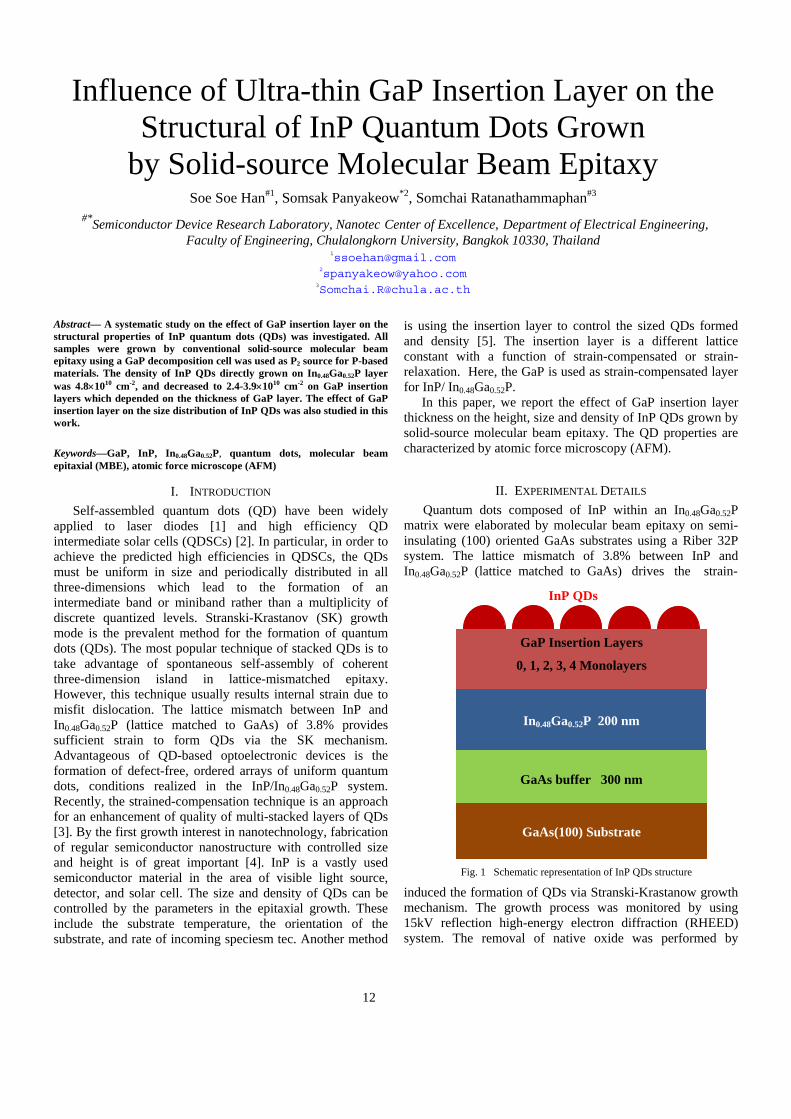
Quantum dots composed of InP within an In0.48Ga0.52P matrix were elaborated by molecular beam epitaxy on semi-insulating (100) oriented GaAs substrates using a Riber 32P system. The lattice mismatch of 3.8% between InP and In0.48Ga0.52P (lattice matched to GaAs) drives the strain-
induced the formation of QDs via Stranski-Krastanow growth mechanism. The growth process was monitored by using 15kV reflection high-energy electron diffraction (RHEED) system. The removal of native oxide was performed by
GaP Insertion Layers
0, 1, 2, 3, 4 Monolayers
GaAs(100) Substrate
GaAs buffer 300 nm
In0.48Ga0.52P 200 nm
InP QDs
Fig. 1 Schematic representation of InP QDs structure
13
heating the substrate under As4 beam at 600°C until the streaky pattern appeared. After oxide desorption, a 300 nm thick GaAs buffer layer was grown at 580°C and followed by a 200 nm In0.48Ga0.52P grown at 480°C. After the deposition of 300 nm GaAs, the growth was interrupted to change from As to P rich ambient. Then, GaP insertion layers with 0-4 monolayers were grown prior the growth of InP QDs. Finally, the QDs were fabricated by deposited 3ML InP with temperature of 450°C at growth rate 0.5 ML/s. The relatively low temperature was chosen in order to inhibit In incorporation from the barrier into the QDs during their self-assembly [6]. The samples were characterized their surface morphology by atomic force microscopy (AFM). Schematic representation of the InP QDs structure with 0-4 ML GaP insertion layer is depicted in Fig. 1.
III. RESULTS AND DISCUSSION
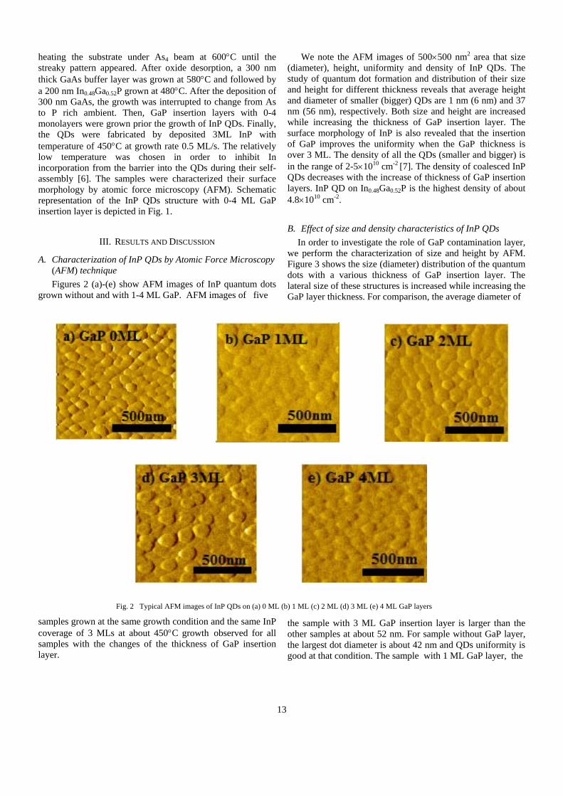
A. Characterization of InP QDs by Atomic Force Microscopy (AFM) technique Figures 2 (a)-(e) show AFM images of InP quantum dots
grown without and with 1-4 ML GaP. AFM images of five
samples grown at the same growth condition and the same InP coverage of 3 MLs at about 450°C growth observed for all samples with the changes of the thickness of GaP insertion layer.
We note the AFM images of 500×500 nm2 area that size (diameter), height, uniformity and density of InP QDs. The study of quantum dot formation and distribution of their size and height for different thickness reveals that average height and diameter of smaller (bigger) QDs are 1 nm (6 nm) and 37 nm (56 nm), respectively. Both size and height are increased while increasing the thickness of GaP insertion layer. The surface morphology of InP is also revealed that the insertion of GaP improves the uniformity when the GaP thickness is over 3 ML. The density of all the QDs (smaller and bigger) is in the range of 2-5×1010 cm-2 [7]. The density of coalesced InP QDs decreases with the increase of thickness of GaP insertion layers. InP QD on In0.48Ga0.52P is the highest density of about 4.8×1010 cm-2.
B. Effect of size and density characteristics of InP QDs In order to investigate the role of GaP contamination layer,
we perform the characterization of size and height by AFM. Figure 3 shows the size (diameter) distribution of the quantum dots with a various thickness of GaP insertion layer. The lateral size of these structures is increased while increasing the GaP layer thickness. For comparison, the average diameter of
the sample with 3 ML GaP insertion layer is larger than the other samples at about 52 nm. For sample without GaP layer, the largest dot diameter is about 42 nm and QDs uniformity is good at that condition. The sample with 1 ML GaP layer, the
Fig. 2 Typical AFM images of InP QDs on (a) 0 ML (b) 1 ML (c) 2 ML (d) 3 ML (e) 4 ML GaP layers

14
average dots size increases to 45 nm and dots uniformity is declined. For samples with GaP insertion layers thickness of 2 to 4 ML, the average dots size also increases to 45, 49, and 48 nm, respectively and dots uniformity is declined.
However for increasing GaP insertion layer thickness, the size of the quantum dot is increased and the uniformity is declined as shown the regularity of their distributions in Fig 3. The sample of 4 ML GaP insertion layer, the QDs size is not clearly different from the sample of 3 ML GaP layer. Although this may be due to thicker insertion layer, it is likely that most of the extra material comes from the exposed GaP surface through In/Ga exchange which may be further enhanced by strain as As/P exchange [8]. In addition to the indium segregation, the In/Ga exchange reaction affects the aasd
Figure 4 shows height histograms of InP QDs that were
indium atoms migrate to the top of dots driven by strain energy to decrease the total system energy and form excess InP QDs nucleation on GaP layer. The exchange reaction
occurs at the places through the thin GaP insertion layer which are covered by the dots. The free InP recombining with P atoms. This leads to bigger QDs as noted in the AFM images.
Fig. 4 shows height histograms of InP QDs that extracted from 500×500 nm2 AFM images. The average height of all samples was nearly the same. A comparison of samples with 0 and 1 MLs of GaP insertion layer, they are the same average height at about 4 nm. The height of 2, 3 and 4 MLs GaP insertion layer samples are slightly decreased. When the thicker GaP insertion layer is grown between QDs and In0.48Ga0.52P layer, the height of the InP QDs increase and the dots become less uniform in terms of size and composition distribution due to suppression of the exchange reaction as noted in the AFM images. The sample without GaP insertion layer showed a significantly improved size, height dispersion and homogeneity. According to the similar effect of QDs diameter, the segregated indium atom may react with P bond during the growth of InP QDs and forms additional InP which
Nu
mb
er o
f d
ots
(%)
Nu
mb
er o
f d
ots
(%)
Diameter (nm)
Fig. 3 Size (diameter) distribution histograms of InP QDs on (a) 0 ML (b) 1 ML (c) 2 ML (d) 3 ML and (e) 4 ML GaP layers Height (nm)
Fig. 4 Height distribution histograms of InP QDs on (a) 0 ML (b) 1 ML (c) 2 ML (d) 3 ML and (e) 4 ML GaP layers
15
increased the QD height and its non-uniformity. Furthermore, the size and height fluctuation was minimal under the effect of strain compensation layer.
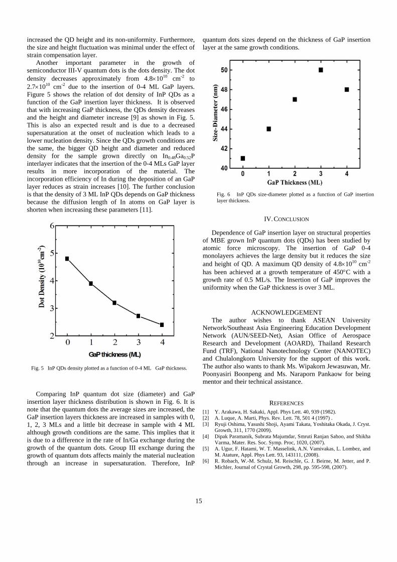
Another important parameter in the growth of semiconductor III-V quantum dots is the dots density. The dot density decreases approximately from 4.8×1010 cm-2 to 2.7×1010 cm-2 due to the insertion of 0-4 ML GaP layers. Figure 5 shows the relation of dot density of InP QDs as a function of the GaP insertion layer thickness. It is observed that with increasing GaP thickness, the QDs density decreases and the height and diameter increase [9] as shown in Fig. 5. This is also an expected result and is due to a decreased supersaturation at the onset of nucleation which leads to a lower nucleation density. Since the QDs growth conditions are the same, the bigger QD height and diameter and reduced density for the sample grown directly on In0.48Ga0.52P interlayer indicates that the insertion of the 0-4 MLs GaP layer results in more incorporation of the material. The incorporation efficiency of In during the deposition of an GaP layer reduces as strain increases [10]. The further conclusion is that the density of 3 ML InP QDs depends on GaP thickness because the diffusion length of In atoms on GaP layer is shorten when increasing these parameters [11].
Comparing InP quantum dot size (diameter) and GaP
insertion layer thickness distribution is shown in Fig. 6. It is note that the quantum dots the average sizes are increased, the GaP insertion layers thickness are increased in samples with 0, 1, 2, 3 MLs and a little bit decrease in sample with 4 ML although growth conditions are the same. This implies that it is due to a difference in the rate of In/Ga exchange during the growth of the quantum dots. Group III exchange during the growth of quantum dots affects mainly the material nucleation through an increase in supersaturation. Therefore, InP
quantum dots sizes depend on the thickness of GaP insertion layer at the same growth conditions.
IV. CONCLUSION
Dependence of GaP insertion layer on structural properties of MBE grown InP quantum dots (QDs) has been studied by atomic force microscopy. The insertion of GaP 0-4 monolayers achieves the large density but it reduces the size and height of QD. A maximum QD density of 4.8×1010 cm-2 has been achieved at a growth temperature of 450°C with a growth rate of 0.5 ML/s. The Insertion of GaP improves the uniformity when the GaP thickness is over 3 ML.
ACKNOWLEDGEMENT The author wishes to thank ASEAN University
Network/Southeast Asia Engineering Education Development Network (AUN/SEED-Net), Asian Office of Aerospace Research and Development (AOARD), Thailand Research Fund (TRF), National Nanotechnology Center (NANOTEC) and Chulalongkorn University for the support of this work. The author also wants to thank Ms. Wipakorn Jewasuwan, Mr. Poonyasiri Boonpeng and Ms. Naraporn Pankaow for being mentor and their technical assistance.
REFERENCES [1] Y. Arakawa, H. Sakaki, Appl. Phys Lett. 40, 939 (1982). [2] A. Luque, A. Marti, Phys. Rev. Lett. 78, 501 4 (1997) . [3] Ryuji Oshima, Yasushi Shoji, Ayami Takata, Yoshitaka Okada, J. Cryst.
Growth, 311, 1770 (2009). [4] Dipak Paramanik, Subrata Majumdar, Smruti Ranjan Sahoo, and Shikha
Varma, Mater. Res. Soc. Symp. Proc, 1020, (2007). [5] A. Ugur, F. Hatami, W. T. Masselink, A.N. Vamivakas, L. Lombez, and
M. Atature, Appl. Phys Lett. 93, 143111, (2008). [6] R. Robach, W.-M. Schulz, M. Reischle, G. J. Beirne, M. Jetter, and P.
Michler, Journal of Crystal Growth, 298, pp. 595-598, (2007).
Fig. 5 InP QDs density plotted as a function of 0-4 ML GaP thickness.
Fig. 6 InP QDs size-diameter plotted as a function of GaP insertion layer thickness.

16
[7] S. D. Singh, T. K. Sharma, C. Mukherjee, and S. M. Oak, IEEE, 978, pp. 1728-1733, (2007).
[8] J. Sormunen, J. Riikonen, M. Mattila, M. Sopanen and H. Lipsanen, IOP. Nanotechnology 16, pp 1630-1635, (2005).
[9] S. Barik, H. H. Tan, and C. Jagadish, IEEE, 4244, pp. 454-457, (2006). [10] V.M Ustinov, N.A. Maleev, A.E. Zhukov, A.R. Kovsh, A. Yu. Egorov,
A.V. Lunev, B.V. Volovik, I.L. Krestnikov, Yu.G. Musikhin, N.A. Bert, P.S. Kop’ev, Z.h.I. Alferov, N.N. Ledentsov, D. Bimberg, Appl. Phys. Lett., 74, 2815, (1999).
[11] M.K. Zundel, P. Specht, K.Eberl, N.Y. Jin-Phillipp, F. Phillipp, Appl. Phys. Lett., 71, 2972(1997).