Embed Size (px)
Citation preview
237 Egypt. J. Solids, Vol. (30), No. (2),(2007)
Influence of Gain Suppression on Static and Dynamic Characteristics of Laser Diodes
under Digital Modulation
Safwat W. Z. Mahmoud
Department of Physics, Faculty of Science, Minia University, El-Minia, Egypt.
This paper presents theoretical investigation of the influence of gain suppression on dynamic characteristics of InGaAsP laser diodes under digital modulation. The study is based on numerical solution of the laser rate equations in which the bias current is augmented by a digital signal with nor-return to zero coding. The modulation characteristics include the eye diagram, turn-on jitter and quality factor of the modulated laser signal. Nonlinear gain is found to improve the eye-diagram quality by increasing the quality factor and reducing the turn-on jitter. Influence of gain suppression on frequency chirp induced by the temporal carrier-induced variation of the refraction change at high bit rates is also illustrated.
1. Introduction:
Currently, there has been growing interest in utilizing directly modulated laser diodes in high speed and long haul optical telecommunication systems because of their potential low cost, compact size, low power consumption and high optical output power compared with other transmitters employing external modulation schemes. The process of imposing data on the light stream is called modulation. The simplest and most widely used digital modulation scheme is called on-off keying (OOK), where the light stream is turned on or off, depending on whether the data bit is 1 or 0, respectively, as illustrated schematically in Fig. (1). OOK can be achieved either by direct modulation of the laser diode (or light emitting diodes) by a stream of binary bits that represents the transmitted data, or by using an external modulator. Direct modulation is simple and inexpensive because no other devices or components are required for modulation. While the bandwidth of light-emitting diodes is limited to a few hundred megahertz [1], directly modulated semiconductor lasers, such as distributed feedback and vertical cavity surface emitting lasers, exceed this value by a factor of ten or even more reaching 10 GHz [2, 3].
Safwat W. Z. Mahmoud
238
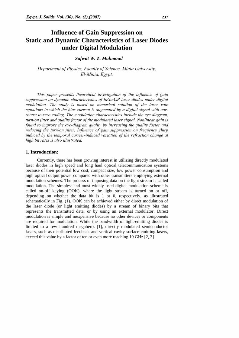
Fig. (1): Direct modulation principle of semiconductor lasers.
As illustrated in Fig. (1), directly modulated lasers are derived by a
current source, which modulates the injected carrier density in the active layer. This carrier density modulation gives rise to phase modulation, which in turn causes variation of the lasing frequency. This frequency variation is referred to as frequency chirping. Under large-signal modulation, chirping represents a form of intrinsic phase modulation that broadens laser lineshape making the laser signal unsuitable for microwave photonics [4]. Also, the broad spectral line limits the ultimate transmission distance within 20km due to its interaction with fiber dispersion along the transmission [5]. Standard single-mode fibers feature minimum loss of 0.2 dB/km at the 1.55 μm wavelength window, however the dispersion is around +17 ps/(nm·km). Thus, a chirped pulse suffers severe distortion which renders this window primarily dispersion-limited. Studying the chirp characteristics of optical sources is therefore essential to estimate precisely the behavior of optical communication systems.
239 Egypt. J. Solids, Vol. (30), No. (2),(2007)
On the other hand, laser operation and dynamics are influenced by property of gain suppression when the laser is biased above threshold, which originates from intraband relaxation processes of injected carriers [6]. The damping rate of laser relaxation oscillations and modulation bandwidth are determined by gain suppression. However, there has been inadequate analysis of the influence of gain suppression on digital modulation characteristics, for instance turn-on jitter and chirping.
In this paper, the rate equation model of semiconductor lasers is used to
study influence of gain suppression on both chirp and modulated intensity characteristics. The present theoretical work is an extension of the simulation model proposed by Ahmed et al. [7] taking into account time fluctuations of the lasing frequency shift. Comprehensive numerical simulations are introduced to study effect of gain suppression on the modulation characteristics when the laser is subjected to digital non-return to zero (NRZ) modulation with gigabit rates. Performance of intensity modulation is determined in terms of turn-on jitter (TOJ) and the quality of the eye diagram. The jitter is defined in general as the misalignment of the significant edges in a sequence of data bits from their ideal positions, resulting in data errors. Tracking these errors over an extended period of time determines the system stability. TOJ is defined as the standard deviation of the random turn-on delay of photon emission after current injection.
The eye diagram is constructed by dividing the laser waveform into
segments of an equal number of bits and overlying each others. The degree of eye opening is evaluated in terms of a laser signal Q-factor [8]. The degree of eye opening, which is an indicator of the modulation performance, is degraded by existence of the quantum noise and TOJ [8]. We show that, increasing of gain suppression over a certain range expected to improve performance of both the laser diode and the laser-based communication systems. Although gain suppression works to reduce the differential efficiency of laser, it improves the modulation characteristics. It helps to generate better laser signal quality, wider eye diagram, lower TOJ, and more reduced peak-to-peak frequency.
2. Theoretical Model:
In this paper, dynamics of single longitudinal mode semiconductor lasers under digital modulation are analyzed in general by solving the following rate equations of the number of injected electrons into the active layer N(t) through the current I(t), photon number S(t), and phase of the optical field θ(t) [9]:
Safwat W. Z. Mahmoud
240
)( )(1 tFNSAtIedt
dNN
s
+−−=τ
(1)
[ ] )( tFNVaSGG
dtdS
Sth ++−=ξ
(2)
( ) )( )(2 tFSNNVat
dtd
θξαπδνθ
+−−== (3)
where δν(t) is the shift of the lasing frequency (chirp) induced by fluctuations in
N(t) around its time-average value N due to change of the phase θ(t) or the refractive index of the active layer. The optical gain G is introduced in the following nonlinear form [10]:
BSAG −= (4)
where A stands for the linear gain coefficient and is given by relation,
( )gNNVaA −=ξ
(5)
with Ng represents the electron number at transparency. The gain coefficient B = GSR×B0 represents the nonlinear (suppressed) term with GSR as a free parameter that gives the gain suppression ratio and B0 is given according to the following linear relationship with respect to N,
( )sin
r
NNaVn
c−⎟
⎠⎞
⎜⎝⎛= R
29B
2
cv
2
02
00
ξτλε
πh
(6)
The term BS in Eqn. (4) measures the gain suppression which affects the damping rate of the relaxation oscillation [11], Gth represents the threshold gain level. In Eqn. (2) α is the line width enhancement factor, which determines the simultaneous variations of the gain and refractive index with the injected carrier number [12]. In Eqn. (3), τs is the electron lifetime due to spontaneous emission. It is defined in the following form to take into account nonradiative recombination processes that are pronounced in semiconductor laser with narrow bandgap energy [7],
VNBeff
s
=τ1
(7)
241 Egypt. J. Solids, Vol. (30), No. (2),(2007)
where Beff is the effective rate of electron recombination including both the radiative and nonradiative recombination processes. Typical parametric values of the considered laser are given in Table (1). The threshold gain level Gth is calculated using the internal loss κ of the active region via the equation:
⎥⎥⎦
⎤
⎢⎢⎣
⎡⎟⎟⎠
⎞⎜⎜⎝
⎛+=
bfrth RRLn
cG 1ln21κ (8)
and is equal to 8.84x10¹⁰s-1. Hence the threshold carrier density can be calculated from the relation:
ξaVG
NN thgth += (9)
and consequently the threshold current is calculated from the following relation
s
thth
eNI
τ= (10)
which gives the value Ith = 3.33 mA. Table 1: typical values of the parameters of a single-mode InGaAsP laser
emitting with λ=1.55μm.
Symbol Meaning Value Unit
a Tangential gain coefficient 7.85x10⁻¹² m3s-1 ξ Field confinement factor of 0.2 --- V Volume of the active region 60 μm3 L Length of the active region 250 μm nr Refractive index of the active region 3.56 --- Ng Electron number at transparency 5.31x10⁷ --- τin Electron intraband relaxation time 0.1 ps
2cvR Squared absolute value of the dipole
moment 9.53x10-57 C2m2
Ns Electron number characterizing nonlinear gain
4.05x10⁷ ---
Beff Effective rate of nonradiative recombination
3.9x10⁻¹⁶ m3s-1
Rf Front facet reflectivity 0.95 -- Rb Back facet reflectivity 0.80 -- Reduced planck's constant 1.05 x10⁻³⁴ Js c Speed of light in free space 3x10⁸ ms-1 ε0 Electrical permittivity of free space 8.85x10⁻¹² Fm-1
Safwat W. Z. Mahmoud
242
As shown in Fig. (1), the deriving current of a digitally modulated laser diode is the sum of two terms. The first term represents the bias current, Ib, which sets the operating point (average power) of the laser. The second term is the modulation current, Im, which determines the modulation level. Both currents are adjusted to achieve the desired average power and extinction ratio (on/off-ratio). The injection current I(t), which is assumed to represent a stream of coded binary bits of the modulating electrical signal, is given in the form
(t)fIItI mmb +=)( (11) where fm(t) is a time varying function with either "0" or "1" level describing the binary bit format of the modulating current. Digital modulation commonly employs either a non-return-to-zero (NRZ) or a return-to-zero (RZ) pseudorandom bit sequence (BRBS) [13].
In Eqs. (1-3), the terms FN(t), FS(t), and Fθ(t) are Langevin noise sources describing the intrinsic fluctuations in S(t), θ(t) and N(t) that are associated with quantum transitions of electrons between the valence and conduction bands. These noise sources have Gaussian statistics and are δ-correlated.
Rate Eqn. (1-3) are nonlinear and coupled. Under large-signal
modulation, their complexity increases which necessitates resorting to numerical techniques to solve them. The Langevin noise sources are generated at instant ti of integration using the values of photon number S(ti-1) and electron number N(ti-1) at the previous instant ti-1 as [9]:
[ ]{ })(1)(2)()(-)()(2)(
)( 1 iiiSiSNiSNiSiNN
iN tFtStFtkgt
tVtktVtF θ++
Δ+
= − , (12)
SiSS
iS gttVtF
Δ=
)()( , (13)
θθ gttV
tStF iSS
ii Δ+
=−
)(1)(
1)(1
, (14)
where VSS and VNN are the autocorrelation coefficients of FS(t) and FN(t), respectively, VSN is their cross-correlation coefficient. These coefficients are given by
[ ] )( 1)( 2)( 11 −− += iiiSS tNtSVatV ξ
, (15)
)( )(1 2)( 11 −− ⎥⎦
⎤⎢⎣
⎡+= ii
siNN tNtS
VatV ξ
τ , (16)
243 Egypt. J. Solids, Vol. (30), No. (2),(2007)
[ ] )(1)( )( )( 111 −−− ++−= igiiiNS tSNtStNVatV ξ (17)
with
)()(
)(iSS
iNSiS tV
tVtk −= . (18)
The Gaussian distributions of these Langevin noise sources are determined by the independent Gaussian random numbers gN, gS, and gθ of zero means and variances of unity.
The power P(t) emitted from the front facet of the laser cavity is calculated from the fluctuating photon number S(t) via the relationship:
( )
( ))(
R-1 R-1
1ln 1
2)(
ff
tS
RR
RRR
LnchtP
bb
bff
r
⎟⎟⎠
⎞⎜⎜⎝
⎛
⎟⎟⎠
⎞⎜⎜⎝
⎛−
=ν (19)
where hν is the photon energy.
3. Numerical Simulation and Results:
The coupled first-order differential Eqn. (1-3) are solved numerically by means of the fourth-order Runge-Kutta method assuming square-pulses of the modulating current in Eqn. (11). The time step of integration Δt is set as short as 2 ps, which corresponds to a cut-off Fourier frequency (=1/Δt) of the laser waveform much higher than the relaxation oscillation frequency. The Gaussian random numbers gN, gS, and gθ characterizing the noise sources FN(t), FS(t) and Fθ(t) in Eqs. (12-14), respectively, are obtained at each integration step by applying the Box-Mueller approximation [14] to a set of three uniformly distributed independent random numbers generated by the computer. The laser is modulated with a NRZ pseudorandom bit stream (PRBS) of word length 27-1. Two bit slots Tb = 500 and 100 ps were considered, which correspond to high gigabit rates of B = 1/Tb = 2 and 10 Gb/s, respectively. The integration is performed over multiple lengths of PBRS in order to collect significant statistics of modulation parameters. The modulation characteristics are simulated as functions of both the biasing current Ib and modulation depth Im. A Fabry-Perot InGaAsP laser emitting with λ = 1.55 μm is considered in the calculations. Typical parametric values of the considered laser are given in Table (1). The corresponding threshold current is Ith = 3.33 mA.
Safwat W. Z. Mahmoud
244
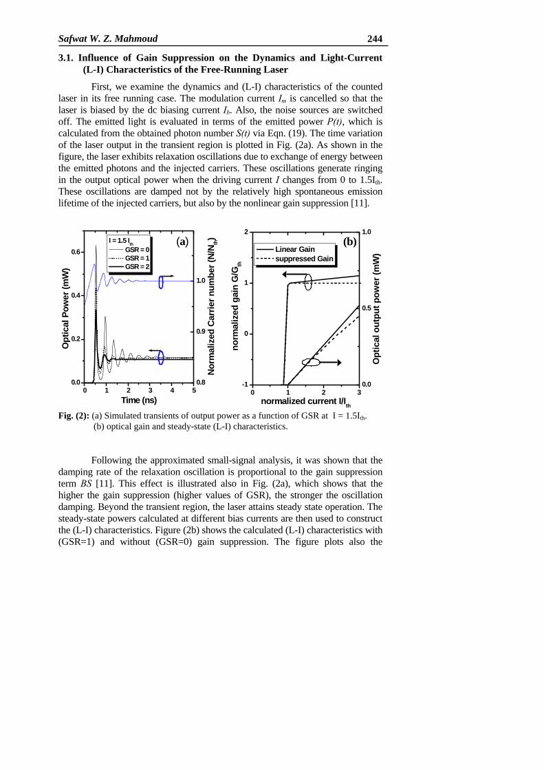
3.1. Influence of Gain Suppression on the Dynamics and Light-Current (L-I) Characteristics of the Free-Running Laser
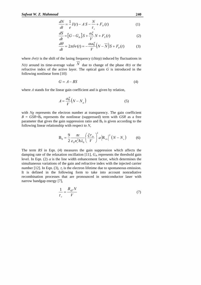
First, we examine the dynamics and (L-I) characteristics of the counted laser in its free running case. The modulation current Im is cancelled so that the laser is biased by the dc biasing current Ib. Also, the noise sources are switched off. The emitted light is evaluated in terms of the emitted power P(t), which is calculated from the obtained photon number S(t) via Eqn. (19). The time variation of the laser output in the transient region is plotted in Fig. (2a). As shown in the figure, the laser exhibits relaxation oscillations due to exchange of energy between the emitted photons and the injected carriers. These oscillations generate ringing in the output optical power when the driving current I changes from 0 to 1.5Ith. These oscillations are damped not by the relatively high spontaneous emission lifetime of the injected carriers, but also by the nonlinear gain suppression [11].
0 1 2 3 4 50.0
0.2
0.4
0.6
0.8
0.9
1.0
(a)
Opt
ical
Pow
er (m
W)
Time (ns)
I = 1.5 Ith GSR = 0 GSR = 1 GSR = 2
Norm
aliz
ed C
arrie
r num
ber (
N/N th
)
0 1 2 3
-1
0
1
2
0.0
0.5
1.0(b)
norm
aliz
ed g
ain
G/G
th
normalized current I/Ith
Linear Gain suppressed Gain
Opt
ical
out
put p
ower
(mW
)
Fig. (2): (a) Simulated transients of output power as a function of GSR at I = 1.5Ith.
(b) optical gain and steady-state (L-I) characteristics.
Following the approximated small-signal analysis, it was shown that the damping rate of the relaxation oscillation is proportional to the gain suppression term BS [11]. This effect is illustrated also in Fig. (2a), which shows that the higher the gain suppression (higher values of GSR), the stronger the oscillation damping. Beyond the transient region, the laser attains steady state operation. The steady-state powers calculated at different bias currents are then used to construct the (L-I) characteristics. Figure (2b) shows the calculated (L-I) characteristics with (GSR=1) and without (GSR=0) gain suppression. The figure plots also the
245 Egypt. J. Solids, Vol. (30), No. (2),(2007)
corresponding variation of optical gain G. The figure shows that G is controlled by the linear part A under threshold; it increases linearly with current I. Above threshold, the linear gain continues increasing linearly but with lower slope, whereas the net gain G is suppressed and clamped at, or even lower than, the threshold level Gth. The figure shows also that contribution of gain suppression is associated with a reduction in the differential efficiency (dP/dI) of the laser diode as represented by the dashed line.
3.2. Characteristics of the Modulated Laser Signal in Time Domain
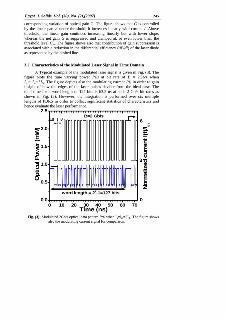
A Typical example of the modulated laser signal is given in Fig. (3). The figure plots the time varying power P(t) at bit rate of B = 2Gb/s when Ib = Im=3Ith. The figure depicts also the modulating current I(t) in order to gain insight of how the edges of the laser pulses deviate from the ideal case. The total time for a word length of 127 bits is 63.5 ns at such 2 Gb/s bit rates as shown in Fig. (3). However, the integration is performed over six multiple lengths of PBRS in order to collect significant statistics of characteristics and hence evaluate the laser performance.
0 10 20 30 40 50 60 700.0
0.5
1.0
1.5
2.0
2.5
word length = 27-1=127 bits
B=2 Gb/s
Opt
ical
Pow
er (m
W)
Time (ns)
000 00
111 1 11 . . . 6
3
0
Nor
mal
ized
cur
rent
I(t)/
I th
Fig. (3): Modulated 2Gb/s optical data pattern P(t) when Ib=Im=3Ith. The figure shows also the modulating current signal for comparison.
Safwat W. Z. Mahmoud
246
As mentioned above, a desired modulated laser signal can be generated by direct injection of the laser diode by an electric signal of suitable format. As shown in Fig. (3), it becomes clear that the optical signal can carry the same information as the modulating electric signal does. There exists a significant difference between the on and off levels of the optical signal such that one can distinguish the 1 and 0 bits. In addition, the bits duration of both the electric signals and the optical ones are identical.
This consistence in time variations of both signals originates from
operation linearity of the laser as given in the L-I characteristics of Fig. (2b). The figure, however, indicates some inferior characteristics of the laser dynamics that deteriorate the modulation performance especially under high bit rates. The laser emission does not begin promptly after injection of the electrical current; instead, it has time delay. This turn-on delay in the 1 bits is random depending on the quantum noise as well as the history of the preceding 0 bits. The moment of these random turn-on times is called the turn-on jitter (TOJ). Another inferior characteristic is the power fluctuations on the on and off levels of the signal. When the modulation depth (Im-Ib) is small, these fluctuations may become large enough to cause errors in identifying the on and off levels [7]. Performance of digital communication systems depends on the amount of TOJ and noise [13].
The eye diagram is a simple visual tool to examine quality of the
modulated signal and qualitatively evaluate performance of digital transmission systems. Long pseudo-random data patterns are often used when generating eye diagrams to guarantee that the eye-diagram virtually represents all symbol transitions. By measuring the width of the eye opening in both vertical and horizontal directions, information about the signal noise and TOJ can be obtained. While jitter contributes to the eye closing in the horizontal direction, noise is indicated by the vertical width of eye diagram. The ideal sampling period to decide opening the eye diagram and whether bit error rates is associated occurs around the instant of maximum vertical opening. This point corresponds to the time at which the signal-to-noise ratio is maximum. Nevertheless, the size and shape of the eye diagram depend on the data rate.
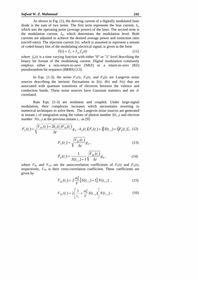
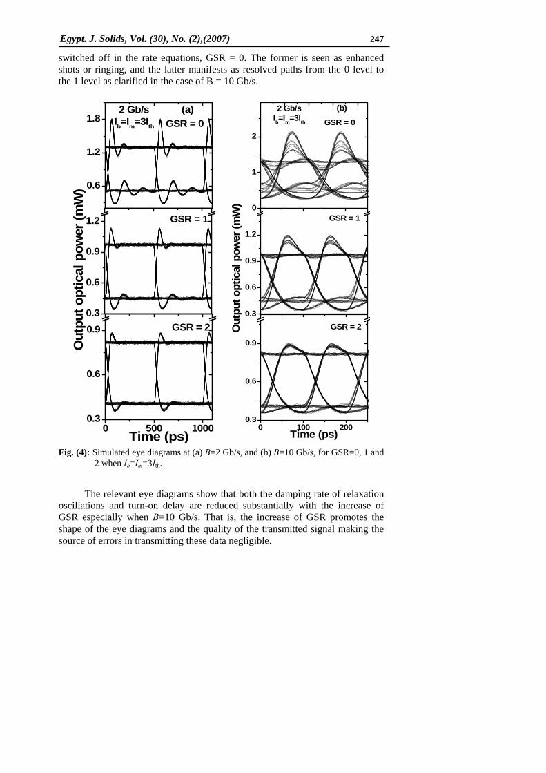
In the present simulations, the eye diagram is constructed by dividing
the stream of P(t) described in Fig. (3) into 3-bit-long segments and overlying each onto others. Figure (4a and b) show two examples of the eye diagram at bit rates B=2 and 10 Gb/s, respectively. Equal bias and modulation currents Ib = Im = 3Ith are applied in both cases, but different gain suppression ratios; namely GSR = 0, 1, and 2, are considered. The figures show that the relaxation oscillations and the turn-on delay are most enhanced when gain suppression is
247 Egypt. J. Solids, Vol. (30), No. (2),(2007)
switched off in the rate equations, GSR = 0. The former is seen as enhanced shots or ringing, and the latter manifests as resolved paths from the 0 level to the 1 level as clarified in the case of B = 10 Gb/s.
0.3
0.6
0.9
1.2
0 500 10000.3
0.6
0.9
0.6
1.2
1.8
0
1
2
0.3
0.6
0.9
1.2
0 100 2000.3
0.6
0.9
GSR = 1
Out
put o
ptic
al p
ower
(mW
)
GSR = 2
Time (ps)
(a)2 Gb/sIb=Im=3Ith GSR = 0
(b)2 Gb/sIb=Im=3Ith GSR = 0
GSR = 1
Out
put o
ptic
al p
ower
(mW
)
GSR = 2
Time (ps)
Fig. (4): Simulated eye diagrams at (a) B=2 Gb/s, and (b) B=10 Gb/s, for GSR=0, 1 and 2 when Ib=Im=3Ith.
The relevant eye diagrams show that both the damping rate of relaxation oscillations and turn-on delay are reduced substantially with the increase of GSR especially when B=10 Gb/s. That is, the increase of GSR promotes the shape of the eye diagrams and the quality of the transmitted signal making the source of errors in transmitting these data negligible.
Safwat W. Z. Mahmoud
248
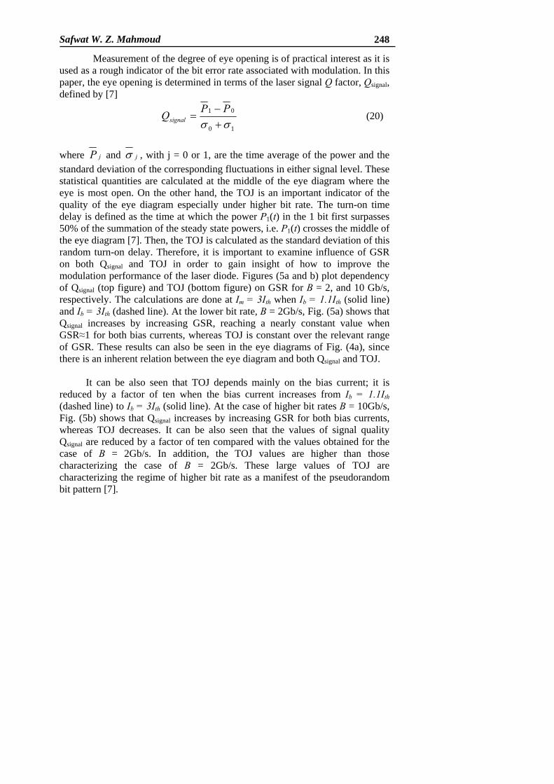
Measurement of the degree of eye opening is of practical interest as it is used as a rough indicator of the bit error rate associated with modulation. In this paper, the eye opening is determined in terms of the laser signal Q factor, Qsignal, defined by [7]
10
01
σσ +−
=PPQsignal (20)
where jP and jσ , with j = 0 or 1, are the time average of the power and the standard deviation of the corresponding fluctuations in either signal level. These statistical quantities are calculated at the middle of the eye diagram where the eye is most open. On the other hand, the TOJ is an important indicator of the quality of the eye diagram especially under higher bit rate. The turn-on time delay is defined as the time at which the power P1(t) in the 1 bit first surpasses 50% of the summation of the steady state powers, i.e. P1(t) crosses the middle of the eye diagram [7]. Then, the TOJ is calculated as the standard deviation of this random turn-on delay. Therefore, it is important to examine influence of GSR on both Qsignal and TOJ in order to gain insight of how to improve the modulation performance of the laser diode. Figures (5a and b) plot dependency of Qsignal (top figure) and TOJ (bottom figure) on GSR for B = 2, and 10 Gb/s, respectively. The calculations are done at Im = 3Ith when Ib = 1.1Ith (solid line) and Ib = 3Ith (dashed line). At the lower bit rate, B = 2Gb/s, Fig. (5a) shows that Qsignal increases by increasing GSR, reaching a nearly constant value when GSR≈1 for both bias currents, whereas TOJ is constant over the relevant range of GSR. These results can also be seen in the eye diagrams of Fig. (4a), since there is an inherent relation between the eye diagram and both Qsignal and TOJ.
It can be also seen that TOJ depends mainly on the bias current; it is
reduced by a factor of ten when the bias current increases from Ib = 1.1Ith (dashed line) to Ib = 3Ith (solid line). At the case of higher bit rates B = 10Gb/s, Fig. (5b) shows that Qsignal increases by increasing GSR for both bias currents, whereas TOJ decreases. It can be also seen that the values of signal quality Qsignal are reduced by a factor of ten compared with the values obtained for the case of B = 2Gb/s. In addition, the TOJ values are higher than those characterizing the case of B = 2Gb/s. These large values of TOJ are characterizing the regime of higher bit rate as a manifest of the pseudorandom bit pattern [7].
249 Egypt. J. Solids, Vol. (30), No. (2),(2007)
10
100
0.0 0.5 1.0 1.5 2.01
10
(a)
Ib = 1.1 Ith Ib = 3.0 Ith
Im = 3 IthB = 2 Gb/s
Qsi
gnal
TOJ
(ps)
Gain Suppression Ratio
0.1
1
10
0.0 0.5 1.0 1.5 2.01
10
(b)
Ib = 1.1 Ith Ib = 3.0 Ith
Im = 3IthB = 10 Gb/s
Qsi
gnal
TOJ
(ps)
Gain Suppression Ratio
Fig. (5): Calculated Qsignal (top) and TOJ (bottom) as functions of GSR for (a) B=2 Gb/s, and (b) B=10 Gb/s. Im=3Ith is kept constant in all cases but with bias currents Ib=1.1Ith (solid line) and Ib=3Ith (dashed line).
3.3. Frequency Chirping:
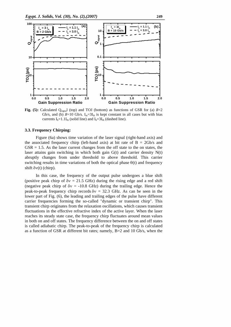
Figure (6a) shows time variation of the laser signal (right-hand axis) and the associated frequency chirp (left-hand axis) at bit rate of B = 2Gb/s and GSR = 1.5. As the laser current changes from the off state to the on states, the laser attains gain switching in which both gain G(t) and carrier density N(t) abruptly changes from under threshold to above threshold. This carrier switching results in time variations of both the optical phase θ(t) and frequency shift δν(t) (chirp).
In this case, the frequency of the output pulse undergoes a blue shift (positive peak chirp of δν = 21.5 GHz) during the rising edge and a red shift (negative peak chirp of δν = -10.8 GHz) during the trailing edge. Hence the peak-to-peak frequency chirp records δν = 32.3 GHz. As can be seen in the lower part of Fig. (6), the leading and trailing edges of the pulse have different carrier frequencies forming the so-called "dynamic or transient chirp". This transient chirp originates from the relaxation oscillations, which causes transient fluctuations in the effective refractive index of the active layer. When the laser reaches its steady state case, the frequency chirp fluctuates around mean values in both on and off states. The frequency difference between the on and off states is called adiabatic chirp. The peak-to-peak of the frequency chirp is calculated as a function of GSR at different bit rates; namely, B=2 and 10 Gb/s, when the
Safwat W. Z. Mahmoud
250
modulation current Im = Ith and 3Ith. Fig. (6b) shows that when GSR increases, δν decreases reaching a minimum value and then increases again. Since there are several parameters come into play, these chirp minima do not correspond to a fixed value of GSR; instead they vary around GSR=1. The calculated values of the peak-to-peak chirp at Im = Ith are comparable to the value of 19 GHz observed in experiments by Sato et al. [15] for 10Gb/s modulation. This correspondence confirms accuracy of the present simulation model and the considered laser parameters. Other features can be traced from Fig. (6b). The frequency chirp increases by increasing both the modulation current and the bit rate. The former effect was observed also in experiments [15]. One can also conclude that GSR can help to minimize the frequency chirp with such a minimum depending on the modulation current and bit rate.
0 5 10 15
-10
0
10
20
30
40
50
0.0
0.5
1.0
RedShift
BlueShift
B=2Gb/sIb=Im=3Ith, GSR=1.5
Freq
uenc
y C
hirp
(GH
z)
Time (ns)
(a)O
ptic
al P
ower
(mW
)
0
20
40
60
0.0 0.5 1.0 1.5 2.00
20
40
60
(b)
Ib = 3Ith, B = 2 Gb/s Im = Ith Im = 3 Ith
B = 10 Gb/s
Peak
-to-P
eak
Freq
uenc
y C
hirp
(GH
z)
Gain Suppression Ratio
Fig. (6): (a) Simulated pulse pattern and frequency chirping when Ib=Im=3Ith and GSR=1.5 at 2Gb/s bit rate, and (B) PP chirp as a function of GSR when Ib=3Ith and at Im=Ith (solid curve) and Im=3Ith. The upper and lower parts stand for 2Gb/s and 10Gb/s bit rates, respectively.
4. Conclusions
Theoretical bases underlying many physical mechanisms of semiconductor laser operation under digital modulation have been presented. The heart of novelty of the present work is that the introduced simulations provide a helpful basis for interpreting the experimental results. The paper demonstrated detailed profiles of optical data pattern, eye diagram and frequency chirping in directly modulated laser diodes. Such profiles are of

251 Egypt. J. Solids, Vol. (30), No. (2),(2007)
practical interest since they represent indicators for modulation performance of data transmission systems. Finally, the increase of gain suppression ratio over a certain range from 0 to 2 is expected to improve performance of both the laser diode and the based communication systems. Although gain suppression works to reduce the differential efficiency of laser, it improves the modulation characteristics. It helps to generate better laser signal quality, wider eye diagram, lower turn-on jitter, and more reduced peak-to-peak frequency.
5. Acknowledgement:
The author would like to thank Dr. Moustafa Ahmed (Physics Dept., Minia University), for valuable discussions.
References:
1. K. J. Ebeling, "Integrated Optoelectronics", Berlin: Springer Verlag, (2006).
2. A. Ramakrishnan, G. Steinle, D. Supper, C. Degen, and G. Ebbinghaus, Electron. Lett. 38 (7), 322 (2002).
3. K. Takagi, A. Shirai, Y. Tatsuoka, C. Watatani, T. Ota, T. Takiguchi, T. Aoyagi, T. Nishimura, and N. Tomita, IEEE Photon. Technol. Lett., 16 (11), 2415 (2004).
4. M. Meliga, C. Coriasso, and R. Paoletti, in LEOS-04, Puerto Rico, Nov. 7-11-2004, 92.
5. G.P.Agrawal and N.K.Dutta, "Long-wavelength semiconductor lasers", Van Nostrand Reinhold Company Inc. (1986).
6. M. Ahmed and M. Yamada, J. Appl. Phys., 84, 3004 (1998). 7. M. Ahmed, M. Yamada and S. W. Z. Mahmoud, J. Appl. Phys., 101 (3),
33119 (2007). 8. G. P. Agrawal and T. M. Shen, Electron. Lett. 22, 450 (1986). 9. M. Ahmed, M. Yamada, and M. Saito, IEEE J. Quantum Electron. 37,
1600 (2001). 10. M. Yamada and Y. Suematsu, J. Appl. Phys. 52, 2653 (1981). 11. M. Ahmed and A. Ellafi, Opt. Laser Technol. 40 (6), 809 (2008). 12. C. H. Henry, J. Lightwave Technol. LT-4, 298, (1986). 13. G. P. Agrawal, "Fiber-optic communication systems", John Wiley and Sons
Inc., New York, (2002) 14. A. Stuart and J. K. Ord, "Advanced Theory of Statistics". London, Griffin,
UK, (1980). 15. K. Sato, S. Kuwahara, and Y. Miyamoto, J. of lightwave Technology, 23
(11), 3790 (2005).


![Turbine suppression[2]](https://img.pdfslide.us/doc/110x75/546d3cafb4af9f662c8b53ba/turbine-suppression2.jpg)