Embed Size (px)
Citation preview

ACTAUNIVERSITATIS
UPSALIENSISUPPSALA
2016
Digital Comprehensive Summaries of Uppsala Dissertationsfrom the Faculty of Science and Technology 1432
Influence of defects and impuritieson the properties of 2D materials
SOUMYAJYOTI HALDAR
ISSN 1651-6214ISBN 978-91-554-9699-9urn:nbn:se:uu:diva-300970

Dissertation presented at Uppsala University to be publicly examined in PolhemsalenÅng/10134, Ångströmlaboratoriet, Lägerhyddsvägen 1, Uppsala, Friday, 11 November2016 at 10:15 for the degree of Doctor of Philosophy. The examination will be conductedin English. Faculty examiner: Dr. Torbjörn Björkman (Åbo Akademi University).
AbstractHaldar, S. 2016. Influence of defects and impurities on the properties of 2D materials.Digital Comprehensive Summaries of Uppsala Dissertations from the Faculty of Science andTechnology 1432. 100 pp. Uppsala: Acta Universitatis Upsaliensis. ISBN 978-91-554-9699-9.
Graphene, the thinnest material with a stable 2D structure, is a potential alternative for silicon-based electronics. However, zero band gap of graphene causes a poor on-off ratio of currentthus making it unsuitable for logic operations. This problem prompted scientists to find othersuitable 2D materials. Creating vacancy defects or synthesizing hybrid 2D planar interfaces withother 2D materials, is also quite promising for modifying graphene properties. Experimentalproductions of these materials lead to the formation of possible defects and impurities withsignificant influence in device properties. Hence, a detailed understanding of the effects ofimpurities and defects on the properties of 2D systems is quite important.
In this thesis, detailed studies have been done on the effects of impurities and defects ongraphene, hybrid graphene/h-BN and graphene/graphane structures, silicene and transitionmetal dichalcogenides (TMDs) by ab-initio density functional theory (DFT). We have alsolooked into the possibilities of realizing magnetic nanostructures, trapped at the vacancy defectsin graphene, at the reconstructed edges of graphene nanoribbons, at the planar hybrid h-BNgraphene structures, and in graphene/graphane interfaces. A thorough investigation of diffusionof Fe adatoms and clusters by ab-initio molecular dynamics simulations have been carried outalong with the study of their magnetic properties. It has been shown that the formation of Feclusters at the vacancy sites is quite robust. We have also demonstrated that the quasiperiodic3D heterostructures of graphene and h-BN are more stable than their regular counterpart andcertain configurations can open up a band gap. Using our extensive studies on defects, we haveshown that defect states occur in the gap region of TMDs and they have a strong signature inoptical absorption spectra. Defects in silicene and graphene cause an increase in scattering andhence an increase in local currents, which may be detrimental for electronic devices. Last butnot the least, defects in graphene can also be used to facilitate gas sensing of molecules as wellas and local site selective fluorination.
Keywords: 2D Materials, Defects on 2D materials, Impurities on 2D materials
Soumyajyoti Haldar, Department of Physics and Astronomy, Materials Theory, Box 516,Uppsala University, SE-751 20 Uppsala, Sweden.
© Soumyajyoti Haldar 2016
ISSN 1651-6214ISBN 978-91-554-9699-9urn:nbn:se:uu:diva-300970 (http://urn.kb.se/resolve?urn=urn:nbn:se:uu:diva-300970)

Dedicated to my parentsand to all my teachers

List of papers
This thesis is based on the following papers, which are referred to in the textby their Roman numerals.
I Magnetic impurities in graphane with dehydrogenated channelsSoumyajyoti Haldar, Dilip Kanhere and Biplab Sanyal.Phys. Rev. B 85, 155426, (2012)
II Functionalization of edge reconstructed graphene nanoribbons byH and Fe: A density functional studySoumyajyoti Haldar, Sumanta Bhandary, Satadeep Bhattacharjee,Olle Eriksson, Dilip Kanhere and Biplab Sanyal.Solid State Communications 152, 1719, (2012)
III Designing Fe nanostructures at graphene/h-BN interfacesSoumyajyoti Haldar, Pooja Srivastava, Olle Eriksson, Prasenjit Senand Biplab Sanyal.J. Phys. Chem. C 117, 21763, (2013)
IV Quasiperiodic van der Waals heterostructures of graphene andh-BNSumanta Bhandary, Soumyajyoti Haldar and Biplab Sanyal.Manuscript.
V Fen(n=1-6) clusters chemisorbed on vacancy defects in graphene:Stability, spin-dipole moment and magnetic anisotropySoumyajyoti Haldar, Bhalchandra S. Pujari, Sumanta Bhandary,Fabrizio Cossu, Olle Eriksson, Dilip Kanhere and Biplab Sanyal.Phys. Rev. B 89, 205411, (2014)
VI Systematic study of structural, electronic, and optical properties ofatomic-scale defects in the two-dimensional transition metaldichalcogenides MX2 (M=Mo,W; X =S, Se, Te)Soumyajyoti Haldar, Hakkim Vovusha, Manoj Kumar Yadav, OlleEriksson and Biplab Sanyal.Phys. Rev. B 92, 235408, (2015)
VII Energetic stability, STM fingerprints and electronic transportproperties of defects in graphene and silicene
Soumyajyoti Haldar, Rodrigo G. Amorim, Biplab Sanyal, Ralph H.Scheicher and Alexandre R. Rocha.RSC Advances 6, 6702, (2016)
VIII Improved gas sensing activity in structurally defected bilayergrapheneY Hajati, T Blom, S H M Jafri, S Haldar, S Bhandary, M Z Shoushtari,O Eriksson, B Sanyal and K Leifer.Nanotechnology 23, 505501, (2012)
IX Site-selective local fluorination of graphene induced by focused ionbeam irradiationHu Li, Lakshya Daukiya, Soumyajyoti Haldar, Andreas Lindblad,Biplab Sanyal, Olle Eriksson, Dominique Aubel, SamarHajjar-Garreau, Laurent Simon and Klaus Leifer.Scientific Reports 6, 19719, (2016)
Reprints were made with permission from the publishers.
Comments on my participation
The works presented in the Papers I to IX have been done in collaboration withother coauthors. Here, I will briefly state my contributions to them. I haveparticipated in all three parts, planning the research, calculations and writingthe manuscript for Papers I – VII. For calculations, there were contributionsfrom PS in Paper III, SB, SB in Paper II, SB in Paper IV, BSP, SB in Paper V,HV, MKY in Paper VI, RGA in Paper VII. PS in Paper III, SB, SB in PaperII, SB in Paper IV and RGA in Paper VII contributed equally in manuscriptwriting. The experiments in Paper VIII – IX were carried out by the groupof KL. In Paper VIII – IX, I have performed the theoretical simulations, haveparticipated in the discussions and have written the corresponding theory part.The IPR calculations in Paper VIII were performed by SB.

Additional publications, but not included in the thesis:
♣ Asystematic study of electronic structure fromgraphene to graphanePrachi Chandrachud, Bhalchandra S Pujari, Soumyajyoti Haldar, Bi-plab Sanyal and D G Kanhere.J. Phys.: Condens. Matter 22, 465502, (2010)
♣ Metallic clusters on a model surface: Quantum versus geometric ef-fectsS. A. Blundell, Soumyajyoti Haldar and D. G. Kanhere.Phys. Rev. B 84, 075430, (2011)
♣ The dipole moment of the spin density as a local indicator for phasetransitionsD. Schmitz, C. Schmitz-Antoniak, A. Warland, M. Darbandi, S. Haldar,S. Bhandary, O. Eriksson, B. Sanyal and H. Wende.Scientific Reports 4, 5760, (2014)
♣ A real-space study of random extended defects in solids: Applicationto disordered Stone–Wales defects in grapheneSuman Chowdhury, Santu Baidya, Dhani Nafday, Soumyajyoti Halder,Mukul Kabir, Biplab Sanyal, Tanusri Saha-Dasgupta, Debnarayan Janaand Abhijit Mookerjee.Physica E 61, 191, (2014)
♣ Influence of Electron Correlation on the Electronic Structure andMagnetism of Transition-Metal PhthalocyaninesIulia Emilia Brumboiu, Soumyajyoti Haldar, Johann Lüder, Olle Eriks-son, Heike C. Herper, Barbara Brena and Biplab Sanyal.J. Chem. Theory Comput. 12, 1772, (2016)
♣ Metal-Free Photochemical Silylations and Transfer Hydrogenationsof Benzene, Polycyclic Aromatic Hydrocarbons and GrapheneRaffaello Papadakis, Hu Li, Joakim Bergman, Anna Lundstedt, KjellJorner, Rabia Ayub, Soumyajyoti Haldar, Burkhard O. Jahn, Aleksan-dra Denisova, Burkhard Zietz, Roland Lindh, Biplab Sanyal, HelenaGrennberg, Klaus Leifer and Henrik Ottosson.Nature Communications 7, 12962, (2016)

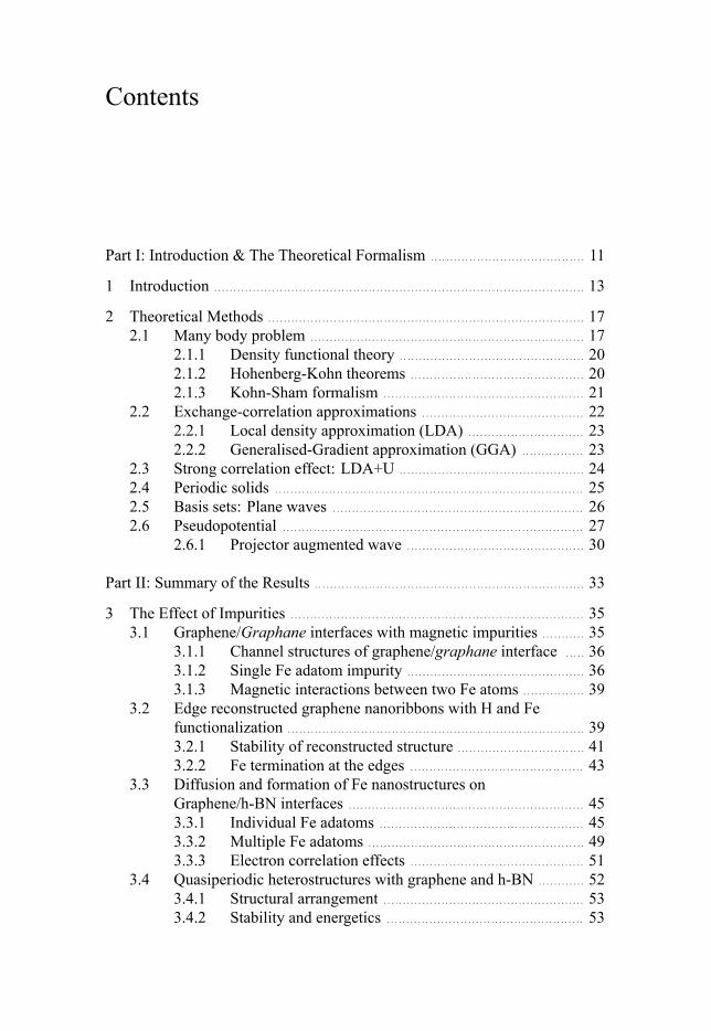
Contents
Part I: Introduction & The Theoretical Formalism . . . . . . . . . . . . . . . . . . . . . . . . . . . . . . . . . . . . . . . . 11
1 Introduction . . . . . . . . . . . . . . . . . . . . . . . . . . . . . . . . . . . . . . . . . . . . . . . . . . . . . . . . . . . . . . . . . . . . . . . . . . . . . . . . . . . . . . . . . . . . . . . . 13
2 Theoretical Methods . . . . . . . . . . . . . . . . . . . . . . . . . . . . . . . . . . . . . . . . . . . . . . . . . . . . . . . . . . . . . . . . . . . . . . . . . . . . . . . . . . 172.1 Many body problem . . . . . . . . . . . . . . . . . . . . . . . . . . . . . . . . . . . . . . . . . . . . . . . . . . . . . . . . . . . . . . . . . . . . . . . 17
2.1.1 Density functional theory . . . . . . . . . . . . . . . . . . . . . . . . . . . . . . . . . . . . . . . . . . . . . . . . 202.1.2 Hohenberg-Kohn theorems . . . . . . . . . . . . . . . . . . . . . . . . . . . . . . . . . . . . . . . . . . . . . 202.1.3 Kohn-Sham formalism . . . . . . . . . . . . . . . . . . . . . . . . . . . . . . . . . . . . . . . . . . . . . . . . . . . . 21
2.2 Exchange-correlation approximations . . . . . . . . . . . . . . . . . . . . . . . . . . . . . . . . . . . . . . . . . . 222.2.1 Local density approximation (LDA) . . . . . . . . . . . . . . . . . . . . . . . . . . . . . . 232.2.2 Generalised-Gradient approximation (GGA) . . . . . . . . . . . . . . . . 23
2.3 Strong correlation effect: LDA+U . . . . . . . . . . . . . . . . . . . . . . . . . . . . . . . . . . . . . . . . . . . . . . . . 242.4 Periodic solids . . . . . . . . . . . . . . . . . . . . . . . . . . . . . . . . . . . . . . . . . . . . . . . . . . . . . . . . . . . . . . . . . . . . . . . . . . . . . . . . 252.5 Basis sets: Plane waves . . . . . . . . . . . . . . . . . . . . . . . . . . . . . . . . . . . . . . . . . . . . . . . . . . . . . . . . . . . . . . . . . 262.6 Pseudopotential . . . . . . . . . . . . . . . . . . . . . . . . . . . . . . . . . . . . . . . . . . . . . . . . . . . . . . . . . . . . . . . . . . . . . . . . . . . . . . 27
2.6.1 Projector augmented wave . . . . . . . . . . . . . . . . . . . . . . . . . . . . . . . . . . . . . . . . . . . . . . 30
Part II: Summary of the Results . . . . . . . . . . . . . . . . . . . . . . . . . . . . . . . . . . . . . . . . . . . . . . . . . . . . . . . . . . . . . . . . . . . . . . 33
3 The Effect of Impurities . . . . . . . . . . . . . . . . . . . . . . . . . . . . . . . . . . . . . . . . . . . . . . . . . . . . . . . . . . . . . . . . . . . . . . . . . . . . 353.1 Graphene/Graphane interfaces with magnetic impurities . . . . . . . . . . . 35
3.1.1 Channel structures of graphene/graphane interface . . . . . 363.1.2 Single Fe adatom impurity . . . . . . . . . . . . . . . . . . . . . . . . . . . . . . . . . . . . . . . . . . . . . . 363.1.3 Magnetic interactions between two Fe atoms . . . . . . . . . . . . . . . . 39
3.2 Edge reconstructed graphene nanoribbons with H and Fefunctionalization . . . . . . . . . . . . . . . . . . . . . . . . . . . . . . . . . . . . . . . . . . . . . . . . . . . . . . . . . . . . . . . . . . . . . . . . . . . . . 393.2.1 Stability of reconstructed structure . . . . . . . . . . . . . . . . . . . . . . . . . . . . . . . . . 413.2.2 Fe termination at the edges . . . . . . . . . . . . . . . . . . . . . . . . . . . . . . . . . . . . . . . . . . . . . 43
3.3 Diffusion and formation of Fe nanostructures onGraphene/h-BN interfaces . . . . . . . . . . . . . . . . . . . . . . . . . . . . . . . . . . . . . . . . . . . . . . . . . . . . . . . . . . . . . 453.3.1 Individual Fe adatoms . . . . . . . . . . . . . . . . . . . . . . . . . . . . . . . . . . . . . . . . . . . . . . . . . . . . . 453.3.2 Multiple Fe adatoms . . . . . . . . . . . . . . . . . . . . . . . . . . . . . . . . . . . . . . . . . . . . . . . . . . . . . . . . 493.3.3 Electron correlation effects . . . . . . . . . . . . . . . . . . . . . . . . . . . . . . . . . . . . . . . . . . . . . 51
3.4 Quasiperiodic heterostructures with graphene and h-BN . . . . . . . . . . . . 523.4.1 Structural arrangement . . . . . . . . . . . . . . . . . . . . . . . . . . . . . . . . . . . . . . . . . . . . . . . . . . . . 533.4.2 Stability and energetics . . . . . . . . . . . . . . . . . . . . . . . . . . . . . . . . . . . . . . . . . . . . . . . . . . . 53
4 The Influence of Defects . . . . . . . . . . . . . . . . . . . . . . . . . . . . . . . . . . . . . . . . . . . . . . . . . . . . . . . . . . . . . . . . . . . . . . . . . . . 574.1 Adsorption and magnetism of Fe cluster on graphene with
vacancy defects . . . . . . . . . . . . . . . . . . . . . . . . . . . . . . . . . . . . . . . . . . . . . . . . . . . . . . . . . . . . . . . . . . . . . . . . . . . . . . 574.1.1 MD results . . . . . . . . . . . . . . . . . . . . . . . . . . . . . . . . . . . . . . . . . . . . . . . . . . . . . . . . . . . . . . . . . . . . . . . . 584.1.2 Correlated vacancies in graphene . . . . . . . . . . . . . . . . . . . . . . . . . . . . . . . . . . . 604.1.3 Interactions of defected graphene with Fen clusters . . . . . 60
4.2 Atomic scale defects in 2D TMD . . . . . . . . . . . . . . . . . . . . . . . . . . . . . . . . . . . . . . . . . . . . . . . . . 634.2.1 Structure and formation energies . . . . . . . . . . . . . . . . . . . . . . . . . . . . . . . . . . . . 654.2.2 Defect concentration at equilibrium . . . . . . . . . . . . . . . . . . . . . . . . . . . . . . . 674.2.3 Electronic structure and optical properties . . . . . . . . . . . . . . . . . . . . 67
4.3 Electronic transport properties of graphene and silicene withdefects . . . . . . . . . . . . . . . . . . . . . . . . . . . . . . . . . . . . . . . . . . . . . . . . . . . . . . . . . . . . . . . . . . . . . . . . . . . . . . . . . . . . . . . . . . . . . 694.3.1 Structures and energetics . . . . . . . . . . . . . . . . . . . . . . . . . . . . . . . . . . . . . . . . . . . . . . . . 704.3.2 Transport properties . . . . . . . . . . . . . . . . . . . . . . . . . . . . . . . . . . . . . . . . . . . . . . . . . . . . . . . . . 72
4.4 Gas sensing activity using defected graphene . . . . . . . . . . . . . . . . . . . . . . . . . . . . . . 744.4.1 Experimental sample preparation and measurements . . . 744.4.2 Theoretical simulations . . . . . . . . . . . . . . . . . . . . . . . . . . . . . . . . . . . . . . . . . . . . . . . . . . . 76
4.5 Site-selective local fluorination of graphene with defects . . . . . . . . . 774.5.1 Sample preparations and experimental results . . . . . . . . . . . . . . 784.5.2 Fluorination of graphene from materials modeling . . . . . . . 79
Part III: Final Conclusions . . . . . . . . . . . . . . . . . . . . . . . . . . . . . . . . . . . . . . . . . . . . . . . . . . . . . . . . . . . . . . . . . . . . . . . . . . . . . . 81
5 Summary and Outlook . . . . . . . . . . . . . . . . . . . . . . . . . . . . . . . . . . . . . . . . . . . . . . . . . . . . . . . . . . . . . . . . . . . . . . . . . . . . . . 835.1 Future prospects . . . . . . . . . . . . . . . . . . . . . . . . . . . . . . . . . . . . . . . . . . . . . . . . . . . . . . . . . . . . . . . . . . . . . . . . . . . . . 85
6 Populärvetenskaplig sammanfattning . . . . . . . . . . . . . . . . . . . . . . . . . . . . . . . . . . . . . . . . . . . . . . . . . . . . . . 89
Acknowledgments . . . . . . . . . . . . . . . . . . . . . . . . . . . . . . . . . . . . . . . . . . . . . . . . . . . . . . . . . . . . . . . . . . . . . . . . . . . . . . . . . . . . . . . . . . . 91
References . . . . . . . . . . . . . . . . . . . . . . . . . . . . . . . . . . . . . . . . . . . . . . . . . . . . . . . . . . . . . . . . . . . . . . . . . . . . . . . . . . . . . . . . . . . . . . . . . . . . . . . . 93

Part I:Introduction & The Theoretical Formalism


1. Introduction
“Where shall I begin, please your Majesty?”he asked. “Begin at the beginning,” the Kingsaid gravely, “and go on till you come to theend: then stop.”
— Lewis Carroll, Alice in Wonderland
Electronics, a field of science and engineering, deals with electronic devicesmade of various electrical components e.g., vacuum tubes, diodes, transistors,integrated circuits, etc. [1]. One of the initial discoveries and inventions inthe history of electronics goes way back in 1745, when Kleist and Musschen-broek invented Leyden jar, which was the original form of capacitor. Sincethen, various inventions and discoveries made by numerous notable scientistsand inventors built a solid foundation in development of electronic technology.However, the invention of diode (the simpler version of vacuum tube) usingthe principle of “Edison Effect” by Fleming in 1905, triggered the beginningof modern electronics. Vacuum tubes became integral part of electronics dur-ing the early part of 20th century and the invention of these vacuum tubesmade the technologies like radio, television, telephone networks, computers,etc. popular and widespread. However, the use of vacuum tubes made thesetechnologies costly and the devices bulky.
Humans have always been mesmerized by the miniaturization’s of modernday electronic devices. The semiconductor devices, which were invented in1940s, made it possible to manufacture smaller, durable, cheaper, and efficientsolid-state devices than vacuum tubes. Consequently, these solid-state devicese.g., transistors, gradually started to replace the vacuum tubes in the electronicdevices during 1950s. In the pursuit of smaller size, integrated circuits (ICs)were invented. The scaling-down of devices is profoundly dependent on thesize of integrated circuits (IC), which are the heart and brain of modern dayelectrical and electronic devices. The ICs are made of large number of tinyelectronic circuits, which are created on a wafer made of pure semiconductormaterial, mainly silicon.
Silicon-based electronics, however, restricts the further scaling down ofsizes. The performance of these electronic devices depend on the mobilityof charge carriers e.g., negatively charged ‘electrons’ and positively charged‘holes’. As the size of these chips are getting smaller and complex, the abil-ity to move electrons around are reaching its practical limits due to amount ofheat dissipation, leakage between the circuits, doping problems, etc. Hence,
13

in pursuit of new materials and technologies as a possible substitute to sili-con is already under way. One of the promising alternative is to use quantumproperties e.g., spin of electrons. The spins of electrons can be aligned eitherup or down, which are alike internal bar magnets. The flipping of spins doesnot require energy to move charge carriers physically, a property that scientistsare eager to use for transporting information in ‘spintronic’ devices. Amongseveral other alternatives [2], such as multigate transistors, III-V compoundsemiconductors, germanium nanodevices, carbon nanotubes, etc., graphene, atwo dimensional monolayer of carbon atoms arranged in a honeycomb lattice[3, 4], has become most promising.
Theoreticians have been studying properties of graphene or ‘2D graphite’for quite sometime since 1950s [3, 5, 6]. However, in 2004, the experimen-tal realization of creating a stable structure of two dimensional (2D) graphenefrom the three dimensional (3D) graphite [4] brought graphene into the lime-light of materials research as the potential alternative to the silicon-based elec-tronics.
So what makes graphene so interesting? The answer lies in some extraor-dinary properties of graphene. First, graphene fits in perfectly for the needof ‘nano’ devices because it is the thinnest material with a highly stable two-dimensional structure. Secondly, graphene has an extremely high charge car-rier mobility even at ambient conditions, 200×103 cm2 V−1 s−1 at a carrierdensity of 1012 cm−2 [7, 8], which remains uninfluenced by temperature, elec-trical or chemical doping. The possibility of tuning charge carriers continu-ously from electron to hole [9], which is known as ambipolar field effect, alsomakes graphene an interesting contender for the device fabrications.
The reason of these exotic properties lies in the fact that the charge car-riers in graphene imitate relativistic particles. Hence, they are described byDirac equation with zero rest mass and effective Fermi velocity vF ≈ 106 ms−1 [10]. This relativistic nature is reflected in remarkable graphene propertieslike anomalous quantum Hall effects (QHE) [11, 12], minimum quantum con-ductivity [13, 14] and Klein tunneling [15]. Ballistic transport is also feasiblein graphene due to its high carrier mobility and long mean free path, which issuitable from the electronic device point of view.
Although graphene has zero carrier density near the Dirac points, it does nothave a band gap and the use of graphene in digital electronics is restricted dueto the occurrence of minimum quantum conductivity. This leads to a very poorIon/Ioff ratio ∼ 101 – 102 [16], which is not suitable for transistor applica-tions. Hence it is necessary to manipulate the properties of graphene. Amongthe various attempts that have been made to introduce a semiconductor gap ingraphene and modify its properties [17–26], creating defects are of particularinterest. The nature and type of defects in graphene have been discussed ex-tensively by Castro Neto et al. [10] and Banhart et al. [27]. Both intrinsic andextrinsic defects are possible in graphene. In particular, graphene is prone to
14

form vacancy defects [28, 29]. Such defects can affect the electronic structureand hence transport properties of graphene [26, 30–32].
The lack of band gap in graphene also prompted scientists to investigateother alternative two dimensional materials with possible band gaps. Thereexist a large number of layered crystalline solid-state materials with weak in-ter layer interaction from which a stable single layer 2D materials can be ex-tracted [33]. These family of “beyond graphene” 2D materials can be classi-fied further in smaller sub-classes such as 2D allotropes (graphyne, borophene,germanene, silicene, stanene, phosphorene), compounds (graphane, hexago-nal boron nitride, germanane, transition metal dichalcogenides, etc.) [17, 21,34–44]. Transition metal dichalcogenides were well known for quite some-times [45] and Frindt et al. have shown that a few and single layer of metaldichalcogenides can be mechanically and chemically exfoliated from the vander Walls layered metal dichalcogenides [46, 47]. However, the potential ofthese 2D materials became apparent after an extraordinary research interest ingraphene. Many of the 2D materials that had not been considered to exist havebeen synthesized using state-of-the-art experimental technologies. These 2Dmaterials can be used in various wide range of applications due to their inter-esting electronic and structural properties, which are quite different from theirbulk counterpart [48–53].
However, to use these various properties in commercial electronic devices,the 2D materials have to be prepared in a scalable way. In today’s available ex-perimental techniques, chemical vapor deposition method has become one ofthe first choices to make large scale fabrication of 2D materials. Nonetheless,defects such as edges, heterostructures, grain boundaries, vacancies, intersti-tial impurities are quite common in CVD prepared samples [27, 54–56]. Thesedefects can be easily observed using various experimental techniques e.g.,transmission electron microscopy (TEM) or scanning tunneling microscopy(STM) [57, 58]. Generally, these defects influence the properties of pristinematerials. Hence it is important to investigate and thoroughly understand therole of defects either for avoiding their formation or for deliberate engineer-ing. Sometimes defects can have destructive effects on device properties [54].However, in nano scale, defects can introduce new functionalities, which canbe beneficial for applications [59, 60].
A parallel approach in modifying graphene properties due to absence ofband gap, is to build a hybrid material involving graphene and other 2D ma-terials. Among other alternative 2D materials [48], hexagonal boron nitride(h–BN) appears to be a perfect candidate in this regard. Hexagonal boron ni-tride is isoelectronic to graphene, has similar lattice constant (only ∼ 1.6 %mismatch), yet having different band structure than graphene, which leads to acomplementary electronic structure [49, 61]. Ab-initio theoretical calculationson these hybrid materials reveal opening of a variable band gap [62–64], carrierinduced magnetism [65], minimum thermal conductance [66] and interfacialelectronic reconstruction [67, 68]. Controlled experimental synthesis of planar
15

hybrid structure of hexagonal boron nitride and graphene sheets with tunableseparate graphene and h–BN regions [69–71] expands a great possibility ofdevice fabrication, e. g., 2D field-effect transistors [72]. Graphane, hydro-genated graphene, is also a very good choice of making hybrid structures withgraphene. These hybrid structures of graphene/graphane can mimic the prop-erties of graphene nanoribbons [73–77]. Hence these materials can be usefulin various potential applications.
In this thesis, we have employed ab-initio density functional theory basedmethods to investigate the influence of defects and impurities on the prop-erties of 2D materials, such as graphene, silicene (2D sheet of silicon), 2Dtransition metal dichalcogenides, hybrid structures of graphene/graphane andgraphene/h-BN. We have also looked into the opportunities of forming mag-netic nanostructures on these interface structures, defected graphene, edge re-constructed zigzag graphene nanoribbons, etc. Transport properties of grapheneand silicene in presence of various kinds of defects have been studied to iden-tify defect-specific signatures. The effects of defects on gas sensing propertiesof graphene and on functionalization of graphene using Fe and F have beendiscussed.
The thesis is arranged in three parts – Part I, II, and III. Part I of thethesis contains two chapters – Introduction in Chapter 1 and brief formalism ofdensity functional theory and computational methods in Chapter 2. The Part IIof the thesis, summary of the results, also contains two chapters – Chapter 3and Chapter 4. Chapter 3 consists of short summaries on the results obtainedinvolving impurities in 2D systems whereas the effects of defects are discussedin Chapter 4. Finally the last part of the thesis, Part III, contains final remarkson the thesis. Here also two chapters are the constituents of this part. Thediscussions about final conclusions and outlooks are contained in Chapter 5.Last but not the least, Chapter 6 contains the summary of this thesis in Swedishlanguage. For more detailed results and discussion, readers are encouraged toread the original research papers and manuscripts attached at the end of thethesis.
16
2. Theoretical Methods
This is the Construct. It is our loadingprogram. We can load anything from clothes,to weapons to training simulations. Anythingwe need.
— Morpheus, The Matrix
Electrons and nuclei are the fundamental particles that determine the physi-cal and chemical characteristics of materials. The atomic and molecular prop-erties such as magnetic, optical, transport and crystal structures of materialsare crucially dependent on the respective electronic structure. Therefore, de-termination of the electronic structure has always been in the focus of con-densed matter physics and chemistry community. However, solutions of theelectronic structure are not straight forward due to the fact that the electronicinteractions in matter are quantum mechanical in nature and the complexity ofdescribing them in a quantum mechanical system increases significantly withthe increasing number of the electrons . This bottleneck leads to the branch ofphysics called “many-body physics”.
2.1 Many body problemThe state of a many particle system is described by all electron wave function,ψ(ri, Rα, t), which in general depends on position and time. The dynamicsfor non-relativistic systems are controlled by a time-dependent Schrödingerequation
iℏ∂ψ
∂t= Hψ . (2.1)
H , the Hamiltonian, represents the total energy operator and has the follow-ing form for a many body system, which consists of a number of interactingelectrons and nuclei
H = − ℏ2
2me
∑i
∇2i −
∑α
ℏ2
2Mα∇2
α −∑i
∑α
Zαe2
|ri − Rα|
+∑i
∑j>i
e2
|ri − rj |+∑α
∑β>α
ZαZβe2
|Rα − Rβ|, (2.2)
17

R1
R3R2
Ra
r1r3
r2ri
Figure 2.1. Schematics of instantaneous positions of atoms and electrons in a manybody system. Small (red) and big (green) circles represent electrons and nuclei respec-tively. Size of the circles are not in scale.
where me and Mα are the mass of electron and αth nucleus respectively,and ri, Rα are the position of ith electron, αth nucleus respectively as de-picted schematically in Fig. 2.1. Zα is the atomic number of the correspond-ing nucleus. The first and the second term of the equation 2.2 are the kineticenergy of the electrons and nuclei, respectively. The remaining three termsare the potential energy due to the Coulomb interaction between electron-nucleus, electron-electron and nucleus-nucleus, respectively. The Hamiltoniandoes not contain any explicit time dependent term. Therefore it is possible towrite the wave function as a simple product of a spatial and a time-dependentparts, ψ
(ri, Rα, t
)= ϕE
(ri, Rα
)e−iEt, which leads to a simpler time-
independent form of equation 2.1
Hψ = Eψ , (2.3)
where E is the total energy of the system.However, solving the Schrödinger equation in this form is limited to a very
small number of systems. Thus, to be applicable for all types of systems, ap-proximations need to be incorporated. The first approximation utilizes the factthat the nuclei are ∼ 103 times heavier compared to the electrons and thus theirmotion are significantly slower than the electronic motion. Thus it is plausi-ble that on the time scale at which the nuclei move, the electrons very rapidlyadapt to the instantaneous position of the configuration of nuclei. Therefore
18
the nuclei wave functions are independent of the electronic coordinates, andthe wave function of the system can be split into the product of nuclei andelectronic terms. This separation of electronic and nuclear motion is knownas the Born-Oppenheimer approximation [78]. Thus the Hamiltonian can beseparated into the nuclei part and the electronic part can be written as follows,
He = − ℏ2
2me
∑i
∇2i −
∑i
∑α
Zαe2
|ri − Rα|+∑i
∑j>i
e2
|ri − rj |. (2.4)
The nuclei-nuclei interaction,∑
α
∑β>α
ZαZβe2
|Rα−Rβ |, is treated classically by the
Ewald method. The total energy of the system is then calculated by adding thisnuclei-nuclei interaction.
Even after this approximation, the solution of the Schrödinger equation isnot easy because of the two following reasons,
1. The number of electrons in solid, N ∼ 1023. Therefore, total 4Nvariables require to describe the many-body electronic wave function.
2. The motion of an electron in solids is affected by the presence of otherelectrons through electron-electron correlation term
∑i
∑j>i
e2
|ri−rj | .Therefore, to obtain any feasible solution, different schemes have been devisedto approximate the many-body problem.
The first approach to solve the problem was introduced by Hartree by con-structing the many electron wave function as a product of single electron wavefunctions. Solving using the variational principle, single particle Hamiltonianequations (Hartree equations) can be found. These equations are similar tothe Schrödinger equation with an effective ‘Hartree’ potential. However, thisapproach does not consider antisymmetric description of the fermionic wavefunction.
Hartree-Fock formalism incorporated this fact by constructing many bodyelectron wave function in a Slater determinant form. By using a variationalmethod, similar Hamiltonian equations can be obtained. However, this for-malism introduces an extra potential, named as exchange potential, along withthe Hartree potential. This formalism is quite successful for small finite sys-tems. However, it does not incorporate any electron correlation effect and thusremains inaccurate.
Both Hartree and Hartree-Fock methods are wave function based. There-fore, they are computationally expensive for large system sizes. The wavefunction is a very complicated quantity which cannot be measured experimen-tally. It depends on 4N variables, three spatial and one spin variable for eachN electrons. Electron density, a real quantity, has reduced degrees of freedomand thus it can reduce the computational expanses significantly, if used as vari-ables. The use of electron density as variable to solve many body Schrödingerequation gives birth to Density Functional Theory, the most popular and ver-satile method in modern day condensed matter physics.
19

2.1.1 Density functional theoryAs stated in the last paragraph, the core concept of Density functional theory(DFT) is that to use the electron density n(r) as a means to reach a solution tothe Schrödinger equation. Thomas and Fermi [79, 80] took the first attempt toobtain information about atomic and molecular systems using electron density.They used a quantum statistical model of electrons which considers only the ki-netic energy of the electrons. Contributions coming from the nuclear-electronand electron-electron were treated in a classical way. In this model Thomasand Fermi derived a very simple expression for the kinetic energy based onnon-interacting uniform electron gas density but excluding the exchange andcorrelation of electrons.
Dirac further extended this model by including exchange interaction termbased on uniform electron gas [81] and modified the equation of kinetic energy.However, the simple approximations by both Thomas-Fermi and Dirac lackedaccurate descriptions of electrons in a many body system, leading to its failure.
2.1.2 Hohenberg-Kohn theoremsThe first strong foundation of DFT came from the formalism of Hohenberg-Kohn in 1964 [82]. Hohenberg and Kohn through their two theorems, firstshowed that the properties of interacting systems can be obtained exactly usingthe ground state electron density, n0(r). This formalism is the core concept ofDFT and relies on the following two theorems*,
Theorem IFor any system of interacting particles in an external potential Vext(r), thepotential Vext(r) can be determined uniquely, except for a constant, by theground state particle density n0(r)Theorem IIA universal functional for the energy E[n] in terms of density n(r) can bedefined, valid for any external potential Vext(r). For any particular Vext(r),the exact ground state energy of the system is the global minimum value ofthis functional, and the density n(r) that minimizes the functional is the exactground state density n0(r)Following the two theorems, the total energy of the system can be written as,
E[n(r)] = F [n(r)] +
∫Vext(r)n(r) dr . (2.5)
The functional F [n(r)] has the following form
F [n(r)] = T [n(r)] + J [n(r)] + Encl[n(r)] , (2.6)
*The statements of the two theorems are directly taken from the book titled “Electronic Structure:Basic Theory and Practical Methods” written by Richard M. Martin. [83]
20
where T [n(r)] is the kinetic energy of the interacting system, J [n(r)] is theHartree term, the classical Coulomb interaction between electrons. Encl[n(r)]is the non-classical electrostatic contributions coming from self-interaction,exchange (i.e., antisymmetric nature of electrons), and electron correlation ef-fects.
Since the functional F [n(r)] does not depend on the external potential, ithas to be same for any system. If the exact form of F [n(r)] were a knownand simple function of n(r), then the ground state energy and density in an ex-ternal potential can easily be determined by the minimization of a functional,which is a function of the three-dimensional density. However, the complex-ities of many electron system remain in finding the accurate form of the uni-versal functional F [n(r)]. The two Hohenberg-Kohn theorems do not provideany solution to determine the exact form of the functional.
2.1.3 Kohn-Sham formalismKohn and Sham, in their article [84], gave a practical approach to obtain theunknown universal functional that we discussed previously. The main ideaof Kohn-Sham formalism was to replace the kinetic energy of the interactingmany-body system (T ) with the exact kinetic energy of a non-interacting sys-tem (TS) built from a set of orbitals, i. e., one electron functions while keepingthe same ground state density. The non-interacting kinetic energy term TS canbe written as,
TS = −1
2
occ∑i=1
⟨ψi|∇2 |ψi⟩ . (2.7)
According to the Kohn-Sham formalism, the total energy functional can bewritten as
E[n(r)] =
∫Vext(r)n(r)dr + TS [n(r)]
+1
2
∫∫n(r)n(r2)
|r − r2|dr dr2 + Exc[n(r)] , (2.8)
where, Vext is the external potential, TS is the kinetic energy term. The thirdterm in the equation is Hartree term, which is the classical electrostatic energyof the electrons. Exc is known as the excahnge-correlation energy and can bedefined using equations 2.5, 2.6 and 2.8 as,
Exc = (T [n(r)]− TS [n(r)]) + Encl[n(r)]
= TC [n(r)] + Encl[n(r)] . (2.9)
Hence, Exc is the functional which contains the residual part of true kineticenergy, TC , and the non-classical electrostatic contributions, Encl. The mini-mization of Kohn-Sham energy functional in equation 2.8, with respect to the
21

electron density n(r) yields a Schrödinger-like Kohn-Sham equation,
HKS(r)ψi(r) =
[−1
2∇2 + VKS(r)
]ψi(r) = εiψi(r) , (2.10)
showing that the non interacting particles are moving in an effective potential,VKS . The potential, VKS , can be written as,
VKS(r) = Vext(r) + VH(r) + Vxc(r) , (2.11)
where, Vext is the external potential, VH is the Hartree potential and Vxc is theexchange-correlation potential. The form of these potentials are expressed as,
VH =
∫n(r2)
|r − r2|dr2 and Vxc =
δExc[n(r)]
δn(r).
ψi are the eigenfunctions and εi are the corresponding eigenvalues. The groundstate electron density can be calculated as follows,
n(r) =
occ∑i=1
|ψi(r)|2 . (2.12)
The newly calculated electron density can be used to calculate new effectivepotential self-consistently. From the equation 2.7 and 2.10, the kinetic energyof the non-interacting system can be written as
TS [n(r)] =
occ∑i=1
εi −∫VKS(r)n(r) dr , (2.13)
and then substituting the value of TS [n(r)] in equation 2.8, the total energy canbe obtained by the following expression,
E[n(r)] =
occ∑i=1
εi −1
2
∫∫n(r)n(r2)
|r − r2|dr dr2
−∫Vxc(r)n(r) dr + Exc[n(r)] , (2.14)
where, the total energy functional E[n(r)] does not depend on the externalpotential Vext(r).
2.2 Exchange-correlation approximationsThe Kohn-Sham formalism we have discussed previously is exact. If the formof Exc is exactly known, then this formalism will yield exact ground state of
22
the interacting many-body system. However, the explicit form of theExc func-tional is not known and approximations to the form of Exc have to be intro-duced. Hence, the quality of DFT calculations solely depend on the accuracyof chosen approximation to Exc. Depending on the level of approximation,different forms of Exc can be constructed. Two of the most common used ap-proximations are local density approximation (LDA) and generalized gradientapproximation (GGA).
2.2.1 Local density approximation (LDA)Hohenberg and Kohn proposed the first ever form of exchange-correlation en-ergy [82]. In this proposal, the exchange-correlation energy density εunixc [n(r)]of a system is considered to be the same as associated with the uniform elec-tron gas with a density n(r). Using this assumption, the form of exchange-correlation functional can be written as below,
ELDAxc [n(r)] =
∫n(r)εunixc [n(r)] dr , (2.15)
where εunixc [n(r)] denotes the exchange-correlation energy density of a uniformelectron gas with density n(r) calculated locally at a point r. This is the mostbasic form of exchange-correlation functional and works quite well for manysystems. εxc has two contributions, exchange, εx, and correlation, εc. Theanalytical form of εx can be evaluated from the approximation of Hartree-Fockexchange and originally derived by Dirac [81] as follows,
εx[n(r)] = −3
4
(3 n(r)
π
) 1
3
. (2.16)
However, the explicit analytical form of εc is not known. Ceperley and Alderobtained highly accurate numerical values of εc using quantum Monte-Carlosimulations of the homogeneous electron gas [85]. On the basis of this nu-merical values, using advanced interpolation techniques, various analytical ex-pressions of εc were presented by different authors e.g., Perdew-Zunger [86]Perdew-Wang [87].
Despite its simplicity, LDA seems to work fine particularly for the molecu-lar properties determination such as equilibrium structures, harmonic frequen-cies or charge moments, properties of itinerant magnetic systems [88]. LDA,however, underestimates the lattice constant of the materials [89] and producerelatively higher binding energies i. e., over binding.
2.2.2 Generalised-Gradient approximation (GGA)Generalized-Gradient approximation was developed to overcome some of thelimitations of LDA. In this method, the exchange-correlation density depends
23
both on the electronic density, n(r), and on the gradient of the electronic den-sity, ∇n(r). GGA exchange-correlation energy is obtained by modifying theLDA energy density:
EGGAxc [n(r)] =
∫n(r)εunixc [n(r)]Fxc [n(r),∇n(r)] dr (2.17)
where Fxc[n(r),∇n(r)] is an analytic function, known as the enhancementfunction. Perdew and Wang provided a parameter free form of exchange en-hancement factor [90]. It was later on modified by Perdew, Burke and Ernz-erhof to give a simplified form, known as PBE after their names. Using aparametrized form of the homogeneous electron gas correlation energy and agradient dependent term, the GGA correlation can also be constructed [91, 92].
GGA corrected the over binding problem of LDA. It also improves the re-sults in structural properties, bulk phase stability, atomic and molecular en-ergies, phase transitions, cohesive energies, etc. However, GGA does notprovide much improvements over LDA in describing itinerant magnetic sys-tems [88].
Although both LDA and GGA are successful in describing some materialproperties, both of them underestimate the band gap of semiconductors andinsulators. The dependence of energy functionalE(N) on the number of elec-trons,N , creates the problem for both LDA and GGA.E(N) and its derivative∂E/∂N , both are continuous for an integral value ofN . However, the deriva-tive of the exact functional might be discontinuous with respect to number ofelectrons. This contributes to the band gap by a significant amount [93, 94].
2.3 Strong correlation effect: LDA+UBoth LDA and GGA failed to describe the band gap problem in materials,where electrons are localized and strongly interacting, such as Mott insulators,transition metal oxides and rare earth compounds. The problem lies in the factthat both LDA and GGA fail to reproduce orbital energies†.
A correction to both the LDA and the GGA energy functional has been in-troduced by incorporating explicit Coulomb interaction of localized electrons(U) in a Hartree-Fock (HF) like approach. This method is commonly known asthe LDA+U correction where “LDA+U” stands for LDA- or GGA calculationcoupled with orbital dependent interaction. In LDA+U approach, the electronsare divided in two different subsystems,
I. localized electrons for which explicit Coulomb interaction is taken intoaccount.
II. wide band electrons, which are described by the LDA.
†Orbital energy ⇒ εi = ∂E/∂ni, ni is the orbital occupation number.
24

Instead of density, density matrix elements ρ were used to define the cor-rected energy functional as follows,
ELDA+U [nσ(r), ρσ] = ELDA [nσ(r)] + EU [ρσ]− Edc [ρσ] ,(2.18)
where, nσ(r) is the charge density for electrons with spin σ. The first term isthe Kohn-Sham energy functional. The second term describes the HF correc-tion to the functional.
The third term in equation 2.18 is known as double counting term. Thisterm has to be subtracted from the total energy functional because the energyfunctional given by LDA already consists of a contribution from the electron-electron interaction.
2.4 Periodic solidsThe above formalism discussed so far is applicable for systems with finite num-ber of electrons, e. g., atoms and molecules. However, in solid systems thecalculation of electronic structure faces problems because of infinitely manyelectrons. This can be overcome by employing the periodicity of the solids.In a single particle context, the electrons feel an effective potential, VKS , pro-vided by the KS equation.
HKS(r)ψi(r) =
[−1
2∇2 + VKS(r)
]ψi(r) = εiψi(r) . (2.19)
where VKS follows the lattice periodicity,
VKS
(r + R
)= VKS (r) , (2.20)
R is the translational vector, which is same as the periodicity of the Bravislattice. According to Bloch theorem [95], in a periodic crystal, the crystalmomentum k is a good quantum number and enforces a boundary conditionfor the KS wave function, ψ
k,
ψk
(r + R
)= eik·R ψ
k(r) , (2.21)
where ψk(r) is the Bloch wave function,
ψk(r) = eik·r u
k(r) . (2.22)
uk(r) is a periodic function of lattice, u
k(r) = u
k(r + R). The single parti-
cle wave function can be expanded in a complete basis set ϕi,k(r), satisfying
Bloch’s criteria for periodic boundary condition.
ψnk(r) =
∑i
ci,nk
ϕi,k(r) , (2.23)
25

where ci,nk
is the Fourier expansion coefficient. Using equation 2.23 in equa-
tion 2.19 and multiplying from the left by⟨ϕi,k
∣∣∣, the following equation canbe written,∑
j
[⟨ϕi,k
∣∣∣HKS
∣∣∣ϕj,k⟩− εnk
⟨ϕi,k|ϕ
j,k
⟩]cj,nk
= 0 . (2.24)
The first and second term in equation 2.24 represents the effective Hamiltonianmatrix element and the overlap matrix element respectively. By solving thefollowing secular equation,
det[⟨ϕi,k
∣∣∣H ∣∣∣ϕj,k⟩− εnk
⟨ϕi,k|ϕ
j,k
⟩]= 0 . (2.25)
the eigenvalues εnk
and the expansion coefficients ci,nk
can be obtained.
2.5 Basis sets: Plane wavesConsiderable number of numerical difficulties still affect the implementationof single particle KS equation. This is due to the fact that the behavior of thewave function is quite different in different regions of space, i. e., in the coreregion and in the valence region. Hence, a complete basis set is needed todescribe the wave function in all the regions of space.
There are several possible choices for the basis sets depending on the sys-tem studied and required accuracy – plane waves (PW), linearized augmentedplane waves (LAPW), localized atomic like orbitals e.g., linear muffin-tin or-bitals (LMTO), linear combination of atomic orbitals (LCAO), etc. In this sec-tion, we will briefly discuss about plane wave basis sets as most of the resultsdiscussed in the thesis are obtained using plane wave based methods.
The lattice periodic function, uj,k(r), can be expressed in a Fourier series
as follows
uj,k(r) =
∑G
cj,G eiG·r , (2.26)
where G is the reciprocal lattice vector, the cj,G are the plane-wave expansioncoefficients, and G.r = 2πm,m being an integer and r is the real space latticevector. Hence the KS orbitals can be expressed in a linear combination of planewaves as
ψjk(r) =
∑G
cjk
(G)× 1√
Ωei(k+G)·r , (2.27)
where cjk
are the expansion coefficient of the wave function in plane wave
basis set ei(k+G).r and G are the reciprocal lattice vectors. It is convenient
26

that the states are normalized and obey periodic boundary condition in a largevolumeΩ, which is allowed to go infinity. Hence, the pre-factor, 1/
√Ω, serves
as the normalization factor. k is the Bloch wave vector. Hence, the KS equationin the notation of Bloch state can be written as(
− ℏ2
2me∇2 + VKS(r)
)ψjk(r) = ε
jkψjk(r) (2.28)
Using equation 2.27 into equation 2.28, and multiplying from the left withe−i(k+G
′).r and integrating over r we get the matrix eigenvalue equation as:∑
G′
(ℏ2
2me
∣∣∣k + G∣∣∣2 δG′ G + VKS
(G− G
′))
cjk
(G)= ε
jkcjk
(G)
(2.29)
In this form, the kinetic energy is diagonal, and the potential, VKS is de-scribed in terms of their Fourier transforms. The solution of equation 2.29is obtained by diagonalization of a Hamiltonian matrix whose matrix elementsH
k+G,k+G′ are given by the terms in brackets on the left hand side. The sizeof the matrix (sum over G′) is determined by the choice of the cutoff energyEcut =
ℏ2
2me
∣∣∣k + Gmax
∣∣∣2, and will be intractably large for systems that con-tain both valence and core electrons. This is a severe problem, but it can beovercome by the use of the pseudopotential approximation, discussed in thenext section.
2.6 PseudopotentialThe pseudopotential approximation deals with the valence electrons of the sys-tem. These rely on the fact that the core electrons are tightly bound to theirhost nuclei, and only the valence electrons are involved in chemical bond-ing. The wave functions of the core electrons do not change significantly withthe environment of the parent atom. Therefore it is possible to combine thecore potential with the nuclear potential, and only deal with the valence elec-trons separately. This method is called Frozen-Core-Approximation (FCA).The physical justification is that almost all the interesting chemical aspects areprimarily related to the outermost (valence) electrons of an atom. The standardpseudopotential model via FCA is schematically shown in Fig. 2.2.
The atomic wave functions are orthogonal to each other. Hence, to maintainthe orthogonality in the neighborhood of nucleus, i. e., in the core region, thevalence electron wave functions must oscillate rapidly. As a result, the kineticenergy of the valence electrons in the core region is quite large and it cancelsout with the potential energy coming from the Coulomb potential. It makes the
27

Valence electronpath
ElectronNucleus
CoreElectrons
Figure 2.2. Schematic diagram of Frozen Core Approximation (FCA) for the standardpseudopotential model. The ion cores composed of the nuclei and tightly bound coreelectrons are treated as chemically inert. Dark green, light green and red circles, re-spectively representing the nucleus, the core electrons and the valence electrons arefor illustrations only (sizes of the circles are not in scale).
valence electron more weakly bound than the core electron. Therefore, one canintroduce an effective pseudopotential, which will be weaker than the strongCoulomb potential in the core region. The pseudo wave function will be node-less and vary smoothly in the core region – so that it can replace the valenceelectron wave function. A schematic representation of pseudopotential methodis presented in Fig. 2.3.
To explain the construction of pseudopotential, following the operator ap-proach [96], let us assume an atom with Hamiltonian H , core states |ψc⟩ withcore energy eigenvaluesEc and valence states |ψv⟩ with valence energy eigen-values Ev. Therefore, the Schrödinger equation can be written as
H |ψi⟩ = Ei |ψi⟩ , (2.30)
where ‘i’ stands for both core and valence states. The goal is to obtain smoothervalence states in the core region. A smoother pseudo-state |ψps⟩ can be definedas
|ψv⟩ = |ψps⟩+∑c
|ψc⟩αcv , (2.31)
where the summation is over core states and αcv is the expansion coefficient.Now, the valence state has to be orthogonal to all of the core states. Hence
⟨ψc|ψv⟩ = 0 = ⟨ψc|ψps⟩+ αcv . (2.32)
28

rc r
Vps
y
aey
ps
Vae
Figure 2.3. Schematic representation of a pseudopotential V ps (red dashed line) andcorresponding pseudo wave function ψps (red dashed line). The pseudo wave functionis node-less and it matches exactly with all electron wave function ψae (green solidline) outside of a cut-off radius rc . This introduces a much softer pseudopotentialcompared to all electron potential V ae ∼ −Z
r .
Inserting the value of αcv from equation 2.32 into equation 2.31,
|ψv⟩ = |ψps⟩ −∑c
|ψc⟩ ⟨ψc|ψps⟩ . (2.33)
Substituting |ψv⟩ both side in equation 2.30 and rearranging we get the follow-ing equation.
H |ψps⟩+∑c
(Ev − Ec) |ψc⟩ ⟨ψc|ψps⟩ = Ev |ψps⟩
⇒ Hps |ψps⟩ = Ev |ψps⟩ . (2.34)
The above equation 2.34 is analogous to the Schrödinger equation with pseudo-Hamiltonian,
Hps = H +∑c
(Ev − Ec) |ψc⟩ ⟨ψc| , (2.35)
and pseudopotential
V ps = Veff +∑c
(Ev − Ec) |ψc⟩ ⟨ψc|
= Veff + Vnl , (2.36)
29

where
Veff = attractive Coulomb potential
and Vnl =∑c
(Ev − Ec) |ψc⟩ ⟨ψc| . (2.37)
The energies described by the pseudo wave functions in equation 2.34, arethe same as that of the original valence states. The effect of the additionalpotential Vnl is localized to the core region and it is repulsive in nature. Hence,it will cancel part of the strong attractive nuclear Coulomb potential Veff , sothat the resulting sum will be a weaker pseudopotential and resulting pseudowave function will be node-less.
2.6.1 Projector augmented waveProjector augmented wave (PAW) method is an all electron method. It com-bines the elegance of plane-wave pseudopotential method with the augmentedwave method. This method was first introduced by Blöchl [97]. As adaptedin pseudopotential method, PAW approach consists of a simpler energy andpotential independent basis but it retains the flexibility of augmented wavemethod. PAW method consists of a linear transformation (Im) linking an os-cillatory true all electron single particle KS wave function |ψn⟩ with a compu-tationally convenient auxiliary wave function, ˜|ψn⟩,
|ψn⟩ = Im ˜|ψn⟩ , (2.38)
where, the index n is a cumulative index representing band, k-point and spin.Using the variational principle with respect to the auxiliary wave function, theKS equation can be transformed as follows,
Im†H Im ˜|ψn⟩ = Im† Im ˜|ψn⟩εn , (2.39)
where Im†H Im = H is the pseudo Hamiltonian and Im† Im = O is the over-lap operator. The purpose of this transformation is to avoid the nodal structureof a true wave function close to the nucleus within a certain radius from thecore, rc (See Fig. 2.3). The wave function inside the core region is modifiedby Im and hence defined as follows,
Im = 1 +∑R
SR . (2.40)
SR is the difference between auxiliary and true single particle KS wave func-tion whileR is the atom site index. SR acts within an augmented space, whichis defined by a cutoff radius, rc ∈ R.
The core wave function is treated separately as it does not expand beyondaugmented region. The energy and the electron density of the core electrons
30

in a material is approximated with an isolated atom calculations‡. Hence, theoperator Im acts on valence wave function and it can be expressed within theaugmented region as follows,
ψ(r) =∑i∈R
ϕi(r)ci . (2.41)
Here ϕi(r) represent the partial wave solutions for Schrödinger equation for anisolated atom and ci are the expansion coefficients associated with it. In thisway, using the transformation Im, the partial wave |ϕi⟩ is one-to-one mappedlocally to an auxiliary partial wave ˜|ϕi⟩.
|ϕi⟩ = (1 + SR)∣∣∣ϕi⟩ for i ∈ R (2.42)
SR
∣∣∣ϕi⟩ = |ϕi⟩ −∣∣∣ϕi⟩ (2.43)
This local transformation implicitly enforces a condition that the partial waves|ϕi⟩ and
∣∣∣ϕi⟩ have to be pairwise identical beyond rc ∈ R:
ϕi(r) = ϕi(r) for i ∈ R and |r − RR| > rc,R (2.44)
Using auxiliary partial wave basis, any arbitrary auxiliary wave function canbe formed within the augmented region,
ψ(r) =∑i∈R
ϕi(r)ci =∑i∈R
ϕi(r)⟨pi | ψ
⟩(2.45)
where, the projector operator |pi⟩ satisfies the following two constraints,∑i∈R
∣∣∣ϕi⟩ ⟨pi| = 1 . . . the completeness relation (2.46)⟨ϕi | pj
⟩= δi,j ; for i, j ∈ R . . . the orthogonality relation (2.47)
In terms of auxiliary and the true partial waves, the transformation operatorcan be written as,
Im = 1 + SR∑i
∣∣∣ϕi⟩ ⟨pi|
= 1 +∑i
(|ϕi⟩ −
∣∣∣ϕi⟩) ⟨pi| (2.48)
‡The frozen-core approximation
31

where the sum runs over the partial waves corresponding to all atoms. Hence,the true wave function can be re-obtained as follows,
|ψ⟩ =∣∣∣ψ⟩+
∑i
(|ϕi⟩ −
∣∣∣ϕi⟩)⟨pi|ψ
⟩=
∣∣∣ψ⟩+∑R
(∣∣ψ1R
⟩−∣∣∣ψ1
R
⟩)(2.49)
where, ∣∣ψ1R
⟩=
∑i∈R
|ϕi⟩⟨pi|ψ
⟩(2.50)∣∣∣ψ1
R
⟩=
∑i∈R
∣∣∣ϕi⟩⟨pi|ψ
⟩(2.51)
As a consequence of this transformation, the wave function is spatially sep-arated out into different parts. Inside the core region, the wave function isexpressed with the partial waves consisting of nodal structure, i. e.,
∣∣∣ψR
⟩=∣∣∣ψ1
R
⟩. This gives the true wave function |ψR⟩ merging to
∣∣∣ψ1R
⟩. Beyond the
core region, both the auxiliary wave functions and the true wave functions areidentical, i. e., |ψR⟩ =
∣∣∣ψR
⟩.
Although the PAW method consists of few approximations, e. g., the frozen-core approximation, expansion of auxiliary wave function with finite numberof plane waves, etc., this method computes to the full wave function, chargeand spin densities with a much simpler basis set.
32

Part II:Summary of the Results


3. The Effect of Impurities
Curiouser and curiouser!— Lewis Carroll, Alice in Wonderland
In this chapter, the effect of impurities on the properties of graphene andrelated hybrid structures, which have been presented in Papers I–IV, will bediscussed in general. As mentioned in the introduction, the studies are mo-tivated by the necessity of altering the semi-metallic nature of pure grapheneto open a band gap. Keeping this aspiration in mind, in the following sec-tions we will discuss: 1) the effects of metallic impurities on two dimensionalhybrid structures of graphene and graphane, 2) exploiting the edge proper-ties of graphene nanostructures using quantum confinement, 3) formation anddiffusion of metallic nanostructures on planar hybrid interfaces of grapheneand hexagonal boron nitride (h-BN) and 4) 3D quasiperiodic heterostructureof graphene and h-BN to break sublattice symmetry.
We have studied the above mentioned systems by performing electronicstructure calculations using plane wave basis sets employing PAW method asimplemented in the VASP [98, 99] code.
3.1 Graphene/Graphane interfaces with magneticimpurities
The interaction of magnetic impurities (Fe adatom in this case) with the hybridstructures of graphene and graphane has been discussed in Paper I.Graphane,one of the important compounds of “beyond grpahene” family of 2D mate-rials, is a hydrogenated graphene structure. In this structure, one hydrogenatom is attached to each carbon atom giving rise to an insulating system withsp3 bonds. This material was first predicted by ab-initio theory [17] and latterexperimentally synthesized [21]. In graphene, a semimetal to metal to insu-lator transition has been observed by varying the concentration of hydrogenatoms [100].
Patterning graphene with partial hydrogenation (hybrid graphene/graphaneinterface) can alter the properties of graphene e.g., in introducing conductingchannels, band gap opening, and magnetically coupled interfaces [100–105].These graphene/graphane interfaces can mimic the edge properties of zigzagor armchair graphene nanoribbons [73–77] and can be used as a potential ma-terial in the field of spintronics research. It has been shown that magnetic
35

properties of transition metal doped zigzag graphene nanoribbons (ZGNR) aremuch more robust as compared to the magnetic moments arising from the edgegeometry [106]. Antiferromagnetic coupling between two edges of ZGNR canbe observed with Fe termination at the edges [107]. Hence, it will be interest-ing to study the effect of Fe adatom, as a representative of magnetic impurities,in these hybrid graphene/graphane interface structures.
3.1.1 Channel structures of graphene/graphane interface
Figure 3.1. Decoration of hydrogen (left) along the diagonal of the unit cell lead-ing to an “armchair” channel and (right) along the edge of the unit cell leading to a“zigzag” channel. In the figure, yellow (light shaded in print) balls are bare carbonatoms, turquoise (dark shades in print) balls are hydrogenated carbon atoms and red(small dark in print) balls are H atoms. For both armchair and zigzag channels, thenanoribbons are 3-rows wide. Reproduced with permission from Paper I. Copyright© 2012 American Physical Society.
We have considered two different graphene/graphane hybrid structures - i)where the hydrogen atoms are removed along the diagonal of the graphanepart to create armchair graphene/graphane superlattices, and ii) where the hy-drogen atoms are removed along the edge of graphane part to create zigzaggraphene/graphane superlattices. In left and right panel of Fig. 3.1, we haveshown a schematic picture of these two structures respectively, for a specificwidth of three rows. The “armchair channel” is nonmagnetic and has a width-dependent band gap. However, the “zigzag channel” interfaces are magnetic.In our simulations, we have used three different widths of channels.
3.1.2 Single Fe adatom impurityWe have placed the Fe adatom at different places on the channels describedabove and optimized the geometries to find out the stable adsorption site. Thecalculated formation energy indicates that the preferred site for Fe adsorptionin the armchair channel is the hollow site inside the graphene region, equidis-tant from the interface. However, Fe adatom prefers to bind at a hollow site
36

Table 3.1. Width dependent energies and magnetic moments of the channel systemswith a single Fe impurity. Eb, µtotal and µFe denote the binding energy of Fe, total mag-netic moment of the system and magnetic moment on Fe site respectively. Reproducedwith permission from Paper I. Copyright © 2012 American Physical Society.
Single Fe atom
Channel Type Channel Width Eb µtotal µFe(eV) (µB) (µB)
Armchair3-rows 1.6 2.0 1.995-rows 1.10 2.06 2.107-rows 0.80 2.00 1.98
Zigzag3-rows 1.38 2.1 2.55-rows 1.42 2.01 2.557-rows 1.45 2.01 2.56
closer to the interface in the zigzag channel. This different behavior is dueto the antiferromagnetic nature of the edge coupling and the position of Feadatom is slightly asymmetric with respect to the surrounding hexagon due tothe stretching of underlying carbon bonds.
Figure 3.2. (Left Panel) Spin-polarized DOS for single Fe atom placed in the three-row “armchair” channel. Total DOS with (blue solid line) and without (red dashedline) Fe. (Right Panel) Spin-polarized DOS for single Fe atom placed in the three-row “zigzag” channel. Total DOS with (blue solid line) and without (red dashed line)Fe. Reproduced with permission from Paper I. Copyright © 2012 American PhysicalSociety.
In Table 3.1, we have shown the energies and magnetic moments of the Featom placed on these channels. Analysis of the binding energies as a functionof channel widths reveals that with increasing width, the binding energy re-mains almost constant in the zigzag channel, while it decreases in the armchairchannel. Total magnetic moment for all the systems are ∼ 2.0 µB , similar tothe value of total magnetic moment of an Fe adatom substitutionaly placed in
37
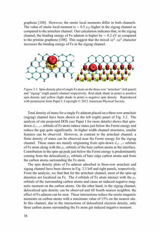
graphene [108]. However, the onsite local moments differ in both channels.The value of onsite local moment is ∼ 0.5 µB higher in the zigzag channel ascompared to the armchair channel. Our calculation indicates that, in the zigzagchannel, the binding energy of Fe adatom is higher by ∼ 0.2 eV as comparedto the pristine graphene [108]. This suggest that the mixed sp2–sp3 characterincreases the binding energy of Fe in the zigzag channel.
Figure 3.3. Spin-density plot of single Fe atom on the three-row “armchair” (left panel)and “zigzag” (right panel) channel respectively. Red (dark shade in print) is positivespin density and yellow (light shade in print) is negative spin density. Reproducedwith permission from Paper I. Copyright © 2012 American Physical Society.
Total density of states for a single Fe adatom placed on a three-row armchair(zigzag) channel have been shown in the left (right) panel of Fig. 3.2. Theanalysis of site projected DOS (see Paper I for more details) shows that spin-down dz2−r2 orbitals of Fe atom induce states just below the Fermi energy andreduce the gap quite significantly. In higher width channel structures, similarfeatures can be observed. However, in contrast to the armchair channel, afinite density of states can be observed near the Fermi energy for the zigzagchannel. These states are mainly originating from spin-down dz2−r2 orbitalsof Fe atom along with the pz orbitals of the bare carbon atoms at the interface.Contribution in the spin-up peak just below the Fermi energy is predominantlycoming from the delocalized pz orbitals of bare edge carbon atoms and fromthe carbon atoms surrounding the Fe atom.
The spin density plots of Fe adatom adsorbed in three-row armchair andzigzag channel have been shown in Fig. 3.3 left and right panels, respectively.From the analysis, we find that for the armchair channel, most of the spin-updensities are localized on Fe. The d orbitals of Fe atom interact with the pzorbitals of the surrounding carbon atoms and cause an induced negative mag-netic moment on the carbon atoms. On the other hand, in the zigzag channel,delocalized spin density can be observed and till fourth nearest neighbor, theeffect of Fe adatom can be seen. These interactions reduce the onsite magneticmoments on carbon atoms with a maximum value of 15% on the nearest site.In this channel, due to the interactions of delocalized electron density, onlythree carbon atoms surrounding the Fe atom get induced negative moment.
38

Effect of spin-orbit couplingWe have also included the spin orbit coupling term in the Hamiltonian in orderto calculate the orbital moments and magnetic anisotropy energies (MAEs).Here, MAE refers to magnetocrystalline energy originating from spin-orbitcoupling. We have neglected the contribution of shape anisotropy. MAE isdefined as ∆E = Ehard − Eeasy. In the armchair channel, the orbital mo-ment of Fe atom is 0.09 µB which is ∼ 0.04 µB higher than the bulk Fe in bccphase. The magnetic anisotropy energy is 19 meV and it has an in-plane easyaxis of magnetization. In case of zigzag channel, with spin orbit coupling, thetotal magnetic moment increases as some of the carbon atoms contribute (∼0.1 µB) additively. Here, the magnetic anisotropy energy with in-plane easyaxis is about 4 meV per Fe atom, which is smaller compared to the value in thearmchair channel. The in-plane orbital moment is 0.1 µB in this case. It is tobe noted that our calculated MAEs for Fe adatom on both channels are quitehigh as compared to the MAE of bulk bcc Fe, which is of the order of 1 µeV.
3.1.3 Magnetic interactions between two Fe atomsIn this subsection, we have discussed the results of two magnetic impurities inthe two channels. In Table 3.2, we have tabulated the binding energies of Featoms, the total magnetic moments, the onsite magnetic moments on Fe atoms,and exchange energies. We have considered various possible Fe-Fe distancesfor both the channels. In the armchair channel, the two Fe atoms are weaklyinteracting which is clear from the small fluctuations of binding energies ofthe Fe atoms with the variation of distances. Hence, the exchange energiesare also small. The analysis of total DOS shows a gap in the spin-up channeljust below the Fermi energy and a gap in the spin-down channel just above theFermi energy. It shows a possibility of creating a “spin gapless semiconductor”in narrower armchair channel occurs.
On the other hand, in the zigzag channel, the binding energies and the mag-netic moments are distance dependent. The two Fe atoms form a dimer forthe smallest Fe-Fe distance. For a Fe-Fe distance of 5.08 Å in all the widths,total magnetic moment decreases with increasing width of channels. It is dueto the fact that, the position of the second Fe atom with respect to the first Featom introduces negative spin moments on the surrounding carbon atoms. SeePaper I for more details.
3.2 Edge reconstructed graphene nanoribbons with Hand Fe functionalization
Another approach towards the opening of band gap in the graphene is to usestructural confinement. Graphene nanoribbons are the one dimensional coun-terpart of 2D graphene. These nanoribbons have various fascinating properties
39

Table 3.2. Width-dependent energies and magnetic moments of the channel systemswith a pair of Fe atoms with possible Fe-Fe distances. The distances between twoFe atoms (d) are in Ångstroms, and the binding energies (Eb) of Fe in are in electronvolts. Total magnetic moment of the systems (µtotal) and the magnetic moments on thetwo Fe atoms (µFe) are in the units of Bohr magneton (the local magnetic momentson two Fe atoms are separately shown by a slash in between them) and the exchangeenergies (Eex = EFM − EAFM ) are in electron volts. Reproduced with permissionfrom Paper I. Copyright © 2012 American Physical Society.
Two Fe atoms in the channel
Type Width dFe Eb µtotal µFe Eex
(Å) (eV) (µB) (µB) (eV)
armchair
3-rows 4.38 3.13 4.02 1.98/2.01 0.0098.77 3.18 4.01 1.99/1.99 0.001
5-rows 4.38 2.25 4.11 2.10/2.10 0.0188.77 2.19 4.08 2.11/2.12 0.008
7-rows 4.38 1.75 4.06 2.04/2.03 0.0148.77 1.64 4.01 2.01/2.01 0.016
zigzag
3-rows2.17 4.12 5.96 2.98/2.98 0.4575.08 2.67 7.0 2.59/2.6 0.0587.60 2.67 4.26 2.42/2.43 0.038
5-rows2.17 4.09 5.89 3.01/3.01 0.8345.08 2.73 4.14 2.53/2.53 NA7.60 2.80 4.06 2.51/2.51 NA
7-rows2.17 4.10 5.82 3.01/3.01 0.7955.08 2.80 4.07 2.53/2.54 NA7.60 2.87 4.02 2.52/2.52 NA
40

e.g., band gap opening, quantum confinement effect, magnetism at the edges,etc [109–111]. Depending on the edge geometry, different types of propertiescan be observed such as metallic behavior in zigzag graphene nanoribbons andsemiconducting behavior in armchair graphene nanoribbons [22, 23]. How-ever, confining the geometry in one dimension to produce graphene nanorib-bons creates unsaturated edges. These edges are quite active and are proneto structural edge reconstruction [74]. Forming pentagon-heptagon pair at theedges is one of the proposed structural rearrangement of graphene nanoribbon.These deformations are quite similar to the Stone-Wales defect observed in 2Dgraphene. These reconstructed zigzag graphene nanoribbon (henceforth called“reczag”) geometry has also been experimentally verified using transmissionelectron microscopy [77]. Ab-initio calculations indicate that reczag structurehas lower total energy as compared to the normal zigzag graphene nanoribbonby 0.35 eV/Å.
In this section and in Paper II, we have discussed the edge reconstruction ofgraphene nanoribbons and functionalization using H and Fe atoms.
3.2.1 Stability of reconstructed structure
(a) (b)
Figure 3.4. (a) Reconstructed edge GNR with 2H termination. Brown balls are Catoms and white balls indicate H atoms. The close-up of the edge structure is alsoshown; (b) Gibbs free energy calculated for 12 rows-reczag. Both 1H and 2H termi-nations with respect to bare reczag are presented. In the inset, transition pressures as afunction of temperatures are shown. P 0 is the reference pressure taken to be 0.1 bar.Reprinted from Paper II, Copyright © 2012, with permission from Elsevier.
Even after reconstruction at the edges, reczag graphene nanoribbons havedangling bonds and these bonds need to be saturated. We have considered edgetermination of each carbon atom by one (1H) and two (2H) hydrogen atoms.The optimized structure of a reczag graphene nanoribbon with 2H termination
41
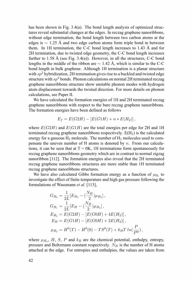
has been shown in Fig. 3.4(a). The bond length analysis of optimized struc-tures reveal substantial changes at the edges. In reczag graphene nanoribbons,without edge termination, the bond length between two carbon atoms at theedges is ∼ 1.25 Å and two edge carbon atoms form triple bond in betweenthem. In 1H termination, the C-C bond length increases to 1.43 Å and for2H termination, due to twisted edge geometry, the C-C bond length increasesfurther to 1.58 Å (see Fig. 3.4(a)). However, in all the structures, C-C bondlengths in the middle of the ribbon are ∼ 1.42 Å, which is similar to the C-Cbond length in bulk graphene. Although 1H termination is a planar structurewith sp2 hybridization, 2H termination gives rise to a buckled and twisted edgestructure with sp3 bonds. Phonon calculations on normal 2H terminated reczaggraphene nanoribbons structure show unstable phonon modes with hydrogenatom displacement towards the twisted direction. For more details on phononcalculations, see Paper II.
We have calculated the formation energies of 1H and 2H terminated reczaggraphene nanoribbons with respect to the bare reczag graphene nanoribbons.The formation energies have been defined as follows
Ef = E(G2H)− [E(G1H) + n ∗ E(H2)] ,
where E(G2H) and E(G1H) are the total energies per edge for 2H and 1Hterminated reczag graphene nanoribbons respectively. E(H2) is the calculatedenergy for a gaseous H2 molecule. The number of H2 molecules used to com-pensate the uneven number of H atoms is denoted by n. From our calcula-tions, it can be seen that at T = 0K, 1H terminations form spontaneously forreczag graphene nanoribbons geometry which are in contrast to normal zigzagnanoribbon [112]. The formation energies also reveal that the 2H terminatedreczag graphene nanoribbons structures are more stable than 1H terminatedreczag graphene nanoribbons structures.
We have also calculated Gibbs formation energy as a function of µH2 toinvestigate the effect of finite temperature and high gas pressure following theformulations of Wassmann et al. [113],
GH2=
1
2L[EH2
− (NH
2)µH2
] ,
GH1=
1
2L[EH − (
NH
2)µH2
] ,
EH2= E(G2H)− [E(G0H) + 4E(H2)] ,
EH = E(G1H)− [E(G0H) + 2E(H2)] ,
µH2= H0(T )−H0(0)− TS0(T ) + kBT ln(
P
P 0) ,
where µH2, H , S, P and kB are the chemical potential, enthalpy, entropy,
pressure and Boltzmann constant respectively. NH is the number of H atomsattached at the edge. For entropies and enthalpies, the values are taken from
42

the tabular data presented in Ref. [114]. We have taken 0.1 bar as the referencepressure, P 0, according to the tabular data. Total energies for 2H, 1H and barereconstructed nanoribbons and hydrogen molecule are indicated as E(G2H),E(G1H), E(G0H) and E(H2) respectively. The calculated values of nor-malized Gibbs energy at 300K have been shown in Fig. 3.4(b). Normalizationwas done by a factor of 2L, where L is the length of unit cell.
From Gibbs energy calculations, it is observed that at room temperatureunder low hydrogen pressure (less than 10−6 bar), 1H terminated edge canbe stabilized over 2H terminated edge. However, after 10−6 bar hydrogenpressure at room temperature, 2H terminated edges are favored. The requiredtransition pressure* as a function of temperature has been shown in the inset ofFig. 3.4(b). The negative values of log10P over a long range of temperature in-dicates the formation of 2H terminated reczag graphene nanoribbons under lowpressure. Hence, following the previous work by Bhandary et al. (Ref. [112])one can conclude that compared to zigzag edges, reczag graphene nanoribbonsare structurally more stable and thus can accommodate higher concentration ofH.
The total density of states calculation for 1H and 2H terminations show finitedensity of states at the Fermi energy. These states mainly originate from thepz orbitals of the C atoms next to the edge C atoms. However, the saturationof C-C bonds at the edges results into the loss of magnetic moment for both1H and 2H terminated reczag graphene nanoribbons.
3.2.2 Fe termination at the edges
Figure 3.5. Spin density isosurfaces of 8-rows Fe doped reczag edge for a FM cou-pling across the edges. Red and blue colors represent spin-up and spin-down densitiesrespectively. Reprinted from Paper II, Copyright © 2012, with permission from El-sevier.
*The amount of hydrogen pressure which favored formation of the 2H terminated edges overthe 1H terminated edges.
43

We have decorated the reconstructed edges of the nanoribbons with mag-netic Fe atoms in order to introduce magnetism and study possible magneticinteractions via graphene lattice. The formation energy Ef of Fe atom at theedge is calculated using the following formula,
Ef = E(metN + reczag)− [N ∗ E(met) + E(reczag)] ,
where E(metN + reczag) is the total energy of metal+reconstructed edgegraphene nanoribbon,E(reczag) is the total energy of reczag graphene nanorib-bon and E(met) is the energy of the Fe calculated in its bulk bcc phase. Nis the number of Fe atoms in the cell. Analysis of geometry and formationenergy reveals that the most stable Fe adsorption site is in between the twoheptagons with a calculated formation energy of 2.6 eV. The Fe adsorptioncauses structural modification at the edges only.
However, the effect of Fe atom at the edge is quite long range which canbe easily observed in spin density isosurface plots as shown in Fig. 3.5. Theonsite local magnetic moment of Fe atom is 3.5 µB , which is quite high andthe Fe atom induces opposite moment to the C atoms to which it is bonded.We have also calculated exchange couplings by calculating the total energydifference between FM and AFM coupling across the edges. The exchangecoupling starts with a strong ferromagnetic coupling for four rows and gradu-ally decreases as the width increases and finally changes to antiferromagneticcoupling after eight rows. This similar oscillatory exchange coupling behav-iors have been in Fe and Co decorated armchair graphene nanoribbons [115].
Figure 3.6. The structures of two dimerized chains indicated as Dimer 1 (left) andDimer 2 (right) in Table 3.3. In the figure, red and yellow balls indicate Fe and Catoms respectively. Reprinted from Paper II, Copyright © 2012, with permission fromElsevier.
We have also investigated the possibility of forming a dimerized chain alongthe nanoribbon edges. Here the Fe atoms bind to the edge carbon atoms ofthe heptagons. Two different dimer configurations are possible as shown inFig. 3.6. The calculation of formation energies tabulated in Table 3.3 indicates
44

Table 3.3. Formation energies (∆E) of two types of Fe dimers in the chain with re-spective to non-dimerized structure. The corresponding bond lengths (short and long)of the Fe dimers are shown for the two structures shown in figure 3.6 along with thelocal magnetic moments at Fe sites. Reprinted from Paper II, Copyright © 2012, withpermission from Elsevier.
Dimer ∆E (eV) Fe-Fe Fe-Fe momentdistance 1 (Å) distance 2 (Å) (µB)
1 -0.23 2.61 2.30 2.942 -0.29 2.77 2.14 2.94
that with increased Fe concentration dimerized chain formation along the edgesof reczag graphene nanoribbons is promoted.
3.3 Diffusion and formation of Fe nanostructures onGraphene/h-BN interfaces
The role of 2D planar Graphene/h-BN interfaces on the designing of Fe nanos-tructures has been presented in Paper III. As discussed in the introduction,the planar graphene/h-BN hybrid sheets can be used to tune the band gap ofgraphene. For most electronic applications, the use of these 2D materials willinvolve contacts with metals. Hence a fundamental understanding of the in-teraction between metals (in the form of adatoms, clusters and thin films, etc.)and hybrid graphene/h-BN interfaces is quite important. Some limited atten-tion has been given in the adsorption of 3d transition metal atoms on hybridgraphene/h-BN structure (1:1 composition of graphene and h-BN) sheets [116].However, a lot of details about the systems still remain unanswered. Giventhis background, in this work, detailed adsorption and diffusion of a single andmultiple Fe adatoms and their magnetic properties on a hybrid graphene/h-BNsheet have been studied. Diffusion barriers were calculated using the climbingimage method within the nudged elastic band (NEB) formalism [117, 118].
3.3.1 Individual Fe adatomsThe structures with completely phase separated graphene and h-BN regionsare energetically the most favorable arrangement for hybrid graphene/h-BNsheets [62–64]. So, a 64 atom hybrid graphene/h-BN supercell, where thegraphene and h-BN regions forming separate domains and being joined byzigzag C–N and C–B interfaces, have been considered for the calculations.We have calculated the adsorption energies for a single Fe adatom placed atdifferent inequivalent hexagonal sites on the 64-atom supercell (see Fig. 3.7).Adsorption energies at these sites and the heights of the Fe adatom from the
45

CB
N
H1
H1´
H1´´H2H3
H4H4´
H4´´
Figure 3.7. Hybrid sheet of graphene/hexagonal boron-nitride showing different sym-metry sites considered for calculation of diffusion barriers. Black solid line representsthe unit cell considered for the calculation. Brown, green and white balls representcarbon, boron and nitrogen atoms respectively. See text for more explanation. Repro-duced with permission from Paper III. Copyright © 2013 American Chemical Society.
surface are mentioned in Table 3.4. We have used these relaxed positions asinitial and final positions to carry out diffusion barrier calculations involvingthe NEB method. Among the hexagonal sites, H4′ turns out to be an unstableone. Our calculation shows that the H3 site at the C–B interface is much lowerin energy than H4′ and hence prevents the formation of an energy barrier fromgoing to H4′ to H3. So an adatom placed at this site moves to the neighboringH3 site at the C–B interface after relaxation. The analysis of adsorption energy(see Table 3.4) clearly shows that the H3 site at the C–B interface is the mostfavorable one followed closely by the H1 site.
Diffusion barriers between all the nearest neighbor hexagonal site (Fig. 3.7)were calculated in both directions using the NEB method. The calculated bar-
Table 3.4. Adsorption energy and the heights of the Fe adatom (Ea) at different sites.Themost stable site is marked in bold. See text for details. Reproducedwith permissionfrom Paper III. Copyright © 2013 American Chemical Society.
Site Ea (eV) Height (Å)
H1 1.65 1.57H1′ 1.36 1.58H1′′ 1.37 1.55H2 0.89 1.65H3 1.74 1.72H4 0.39 1.62H4′′ 0.57 1.90
46
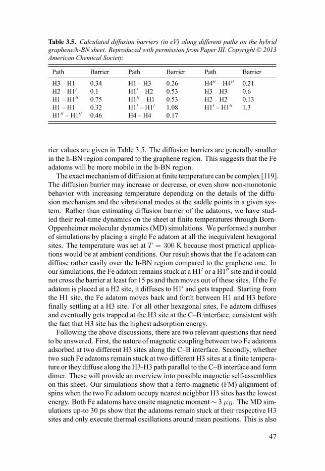
Table 3.5. Calculated diffusion barriers (in eV) along different paths on the hybridgraphene/h-BN sheet. Reproduced with permission from Paper III. Copyright © 2013American Chemical Society.
Path Barrier Path Barrier Path Barrier
H3 – H1 0.34 H1 – H3 0.26 H4′′ – H4′′ 0.21H2 – H1′ 0.1 H1′ – H2 0.53 H3 – H3 0.6H1 – H1′′ 0.75 H1′′ – H1 0.53 H2 – H2 0.13H1 – H1 0.32 H1′ – H1′ 1.08 H1′ – H1′′ 1.3H1′′ – H1′′ 0.46 H4 – H4 0.17
rier values are given in Table 3.5. The diffusion barriers are generally smallerin the h-BN region compared to the graphene region. This suggests that the Feadatoms will be more mobile in the h-BN region.
The exact mechanism of diffusion at finite temperature can be complex [119].The diffusion barrier may increase or decrease, or even show non-monotonicbehavior with increasing temperature depending on the details of the diffu-sion mechanism and the vibrational modes at the saddle points in a given sys-tem. Rather than estimating diffusion barrier of the adatoms, we have stud-ied their real-time dynamics on the sheet at finite temperatures through Born-Oppenheimer molecular dynamics (MD) simulations. We performed a numberof simulations by placing a single Fe adatom at all the inequivalent hexagonalsites. The temperature was set at T = 300 K because most practical applica-tions would be at ambient conditions. Our result shows that the Fe adatom candiffuse rather easily over the h-BN region compared to the graphene one. Inour simulations, the Fe adatom remains stuck at a H1′ or a H1′′ site and it couldnot cross the barrier at least for 15 ps and then moves out of these sites. If the Feadatom is placed at a H2 site, it diffuses to H1′ and gets trapped. Starting fromthe H1 site, the Fe adatom moves back and forth between H1 and H3 beforefinally settling at a H3 site. For all other hexagonal sites, Fe adatom diffusesand eventually gets trapped at the H3 site at the C–B interface, consistent withthe fact that H3 site has the highest adsorption energy.
Following the above discussions, there are two relevant questions that needto be answered. First, the nature of magnetic coupling between two Fe adatomsadsorbed at two different H3 sites along the C–B interface. Secondly, whethertwo such Fe adatoms remain stuck at two different H3 sites at a finite tempera-ture or they diffuse along the H3-H3 path parallel to the C–B interface and formdimer. These will provide an overview into possible magnetic self-assemblieson this sheet. Our simulations show that a ferro-magnetic (FM) alignment ofspins when the two Fe adatom occupy nearest neighbor H3 sites has the lowestenergy. Both Fe adatoms have onsite magnetic moment ∼ 3 µB . The MD sim-ulations up-to 30 ps show that the adatoms remain stuck at their respective H3sites and only execute thermal oscillations around mean positions. This is also
47

evident from the fact that the diffusion barrier between two H3 sites is quitehigh (0.6 eV) as reported in Table 3.5. Hence, the H3 sites truly act as trappingsites for individual Fe adatoms diffusing on the hybrid graphene/h-BN sheetsat the room temperature.
-10 -8 -6 -4 -2 0 2 4 6 8E - E
f (eV)
0
5
10
15
DO
S (
Sta
tes/
eV
)
B at C-B int. (x2)C at C-B int. (x2)
TotalC at C-N int. (x2)
-10 -8 -6 -4 -2 0 2 4E - E
f (eV)
-20
-10
0
10
20
DO
S (
Sta
tes
/ eV
)
Fe-dtotalB-pN-pC-p
Figure 3.8. DOS for (top panel) pure hybrid grphene/h-BN sheet and (bottom panel)a Fe adatom adsorbed at C–B interface of hybrid graphene/h-BN sheet. Reproducedwith permission from Paper III. Copyright © 2013 American Chemical Society.
The analysis of charge density of pure graphene/h-BN sheet shows that atthe C–B interface, the charge density is not homogeneously distributed over theC–B bond whereas the C–N interface has a homogeneous charge distribution(π character originating from C and N pz orbitals) over the C–N bond. Thisasymmetry in the distribution of charge density allows C–B interface to bemore reactive.
The calculated DOS and atom projected DOS (pDOS) for a single Fe adatomtrapped at a H3 site on a 64-atom hybrid graphene/h-BN sheet, shown in Fig. 3.8.For comparison, DOS and atom and site projected DOS of the pure sheet arealso shown. For the sheet without Fe, the valence band states just below thegap come mainly from the C atoms bonded to B atoms at the C–B interface.
48

Conduction band states just above the gap come mainly from the C atoms at theC–N interface. States from both C–B and C–N interfaces appear in the gap ofpure h-BN. In the presence of Fe, those states still persist, but appear only in thedown-spin channel. The analysis ofmℓ projected DOS reveals that for the C–Binterface, Fe dxy orbital hybridizes with B pz orbital quite prominently. Also,Fe dz2 orbital hybridizes with C pz and N pz orbitals. So, a relatively strongbinding scenario has established. The up-spin channel with filled d-states doesnot contribute at the Fermi energy, yielding a half metallic solution. Fe has amagnetic moment of 2.6 µB , whereas a few C atoms close to Fe possess smallnegative moments yielding a total magnetic moment of 2.0 µB in the unit cell.However, for the C–N interface, no significant hybridization (except a smallone between Fe dx2−y2 and B and C pz orbitals) between Fe d orbitals and porbitals of B/C/N is observed.
3.3.2 Multiple Fe adatomsNow that we have gained some understanding of the finite temperature dy-namics of isolated Fe adatoms and magnetic exchange coupling between twoisolated Fe adatoms on the sheet, we now try to shed some light on the ques-tion of clustering and subsequent dynamics when more than one Fe adatomare deposited. Particularly striking was our finding that the H1′ site, in spite ofhaving large barriers, do not trap Fe adatoms, which ultimately get stuck at theH3 sites and thus making finite temperature MD calculations for multiple Feadatoms even more relevant. The analysis of MD simulations, where multipleFe adatoms were placed either in the h-BN or graphene regions, shows thatthe Fe adatoms quickly form a cluster and then the cluster as a whole diffuseseasily and finally gets stuck at the C–B interface. In experiments, one maynot have such microscopic control during the deposition of Fe adatoms on thehybrid graphene/h-BN sheet. Also in view of the fact that CVD experimentsproduce domains of h-BN inside a graphene sheet, the adatoms are equallylikely to land on either of the regions. To simulate that, we consider a largesupercell with 128 atoms: 64 C, 32 B and 32 N atoms. These are divided intotwo graphene and two h-BN regions as shown in Fig. 3.9. Eight Fe adatomsare placed at eight hexagonal sites on this sheet at t = 0 in the following way.Two Fe adatoms are placed in each of the C–1 and C–2 regions, and two Feadatoms each in the BN–1 and BN–2 regions.
Note that there is a C–B interface between C–1 and BN–1 regions (C–B–int1), a C–N interface between BN–1 and C–2 regions (C–N–int1), anotherC–B interface between C–2 and BN–2 (C–B–int2) and finally another C–Ninterface between BN–2 and C–1 (C–N–int2) due to the periodic boundaryconditions. As shown in the second panel of Fig. 3.9, within 3 ps, all the fourFe adatoms in the BN–1 and C–1 regions form a Fe4 cluster. The two Feadatoms placed in the BN–1 region easily move towards the C–B–int1. At the
49
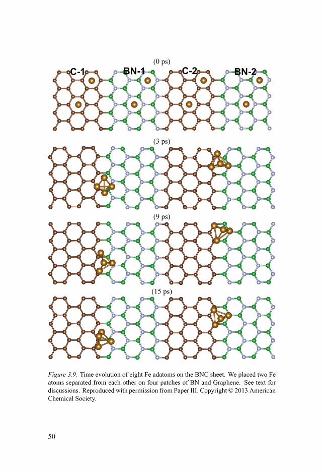
(0 ps)C-1 C-2BN-1 BN-2
(3 ps)
(9 ps)
(15 ps)
Figure 3.9. Time evolution of eight Fe adatoms on the BNC sheet. We placed two Featoms separated from each other on four patches of BN and Graphene. See text fordiscussions. Reproduced with permission from Paper III. Copyright © 2013 AmericanChemical Society.
50
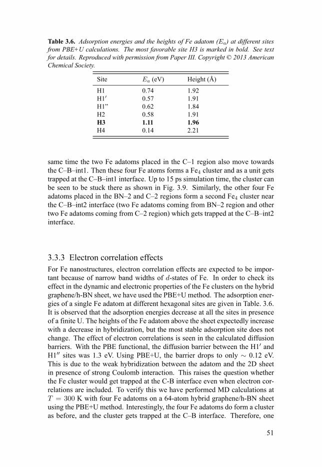
Table 3.6. Adsorption energies and the heights of Fe adatom (Ea) at different sitesfrom PBE+U calculations. The most favorable site H3 is marked in bold. See textfor details. Reproduced with permission from Paper III. Copyright © 2013 AmericanChemical Society.
Site Ea (eV) Height (Å)
H1 0.74 1.92H1′ 0.57 1.91H1” 0.62 1.84H2 0.58 1.91H3 1.11 1.96H4 0.14 2.21
same time the two Fe adatoms placed in the C–1 region also move towardsthe C–B–int1. Then these four Fe atoms forms a Fe4 cluster and as a unit getstrapped at the C–B–int1 interface. Up to 15 ps simulation time, the cluster canbe seen to be stuck there as shown in Fig. 3.9. Similarly, the other four Feadatoms placed in the BN–2 and C–2 regions form a second Fe4 cluster nearthe C–B–int2 interface (two Fe adatoms coming from BN–2 region and othertwo Fe adatoms coming from C–2 region) which gets trapped at the C–B–int2interface.
3.3.3 Electron correlation effectsFor Fe nanostructures, electron correlation effects are expected to be impor-tant because of narrow band widths of d-states of Fe. In order to check itseffect in the dynamic and electronic properties of the Fe clusters on the hybridgraphene/h-BN sheet, we have used the PBE+U method. The adsorption ener-gies of a single Fe adatom at different hexagonal sites are given in Table. 3.6.It is observed that the adsorption energies decrease at all the sites in presenceof a finite U. The heights of the Fe adatom above the sheet expectedly increasewith a decrease in hybridization, but the most stable adsorption site does notchange. The effect of electron correlations is seen in the calculated diffusionbarriers. With the PBE functional, the diffusion barrier between the H1′ andH1′′ sites was 1.3 eV. Using PBE+U, the barrier drops to only ∼ 0.12 eV.This is due to the weak hybridization between the adatom and the 2D sheetin presence of strong Coulomb interaction. This raises the question whetherthe Fe cluster would get trapped at the C-B interface even when electron cor-relations are included. To verify this we have performed MD calculations atT = 300 K with four Fe adatoms on a 64-atom hybrid graphene/h-BN sheetusing the PBE+U method. Interestingly, the four Fe adatoms do form a clusteras before, and the cluster gets trapped at the C–B interface. Therefore, one
51

can safely conclude that the findings from PBE calculations are qualitativelysimilar in the case of PBE+U.
3.4 Quasiperiodic heterostructures with graphene andh-BN
A
B
A
A
A
B
B
B
B
B
A
A
A
A
A
A
A
Figure 3.10. Schematic representation of quasiperiodic Fibonacci stacking ofgraphene and hexagonal boron nitride heterostructure. In inset we have shown theschematics of Bernal stacking that we have used for the stacking the individual layers.
In the previous section (see section 3.3), we have discussed about the pla-nar heterostructure of graphene and h-BN. This idea of heterostructure can beeasily extended to three dimension. Graphene and h-BN have a very good lat-tice matching, which is beneficial for experimental synthesis of high qualitystacked 3D heterostructures [120, 121]. Devices with crystalline graphene onh-BN substrate are found to be work better compared to SiO2 [120]. Giovan-netti et al. have shown in their ab-initio studies that these kind of structurescan induce a bandgap [122]. Experimentally, heterostructures of graphene andh-BN have been synthesized by various groups [123–125]. In these structures,possible metal to insulator transitions [123], band gap tuning [126–128] havebeen observed.
52
In this section and in Paper IV, we have investigated structural as well aselectronic properties of a unique quasiperiodic stacking of h-BN and graphene.
3.4.1 Structural arrangementOur proposed 3D quasiperiodic structure of graphene and h-BN follows a Fi-bonacci sequence, Sj . It follows a recurring relation as shown below,
Sj+1 = Sj , Sj−1;where S0 = B and S1 = AA = graphene single layerB = h-BN single layer
So the first few sequence will be as follows,
S2 = S1, S0 = AB,S3 = S2, S1 = ABA,S4 = S3, S2 = ABAAB, ....
We have schematically shown the Fibonacci sequence in Fig. 3.10. For the ar-rangement of inter layer stacking, we have used Bernal stacking which has beenshown in the inset of Fig. 3.10. We have considered four different heterostruc-tures with 13, 21, 34, 55 layers and henceforth referred as Fib13, Fib21, Fib34,Fib55 respectively. Following the above mentioned Fibonacci sequences, thesefour heterostructures have the following number of BN (NBN ) and graphene(NC) layers,
13 layers = (NBN , NC) = (5, 8) =⇒ Fib1321 layers = (NBN , NC) = (8, 13) =⇒ Fib2134 layers = (NBN , NC) = (13, 21) =⇒ Fib3455 layers = (NBN , NC) = (21, 34) =⇒ Fib55
We have also considered reverse structures by switching the layer composi-tions. These reverse structures have (8, 5), (13, 8), (21, 13) and (34, 21) layersof (NBN , NC). This reversing of structures has two relevance, i) change inthe concentration of graphene and h-BN layers and ii) change of the interfaceordering keeping the number of interfaces unchanged.
3.4.2 Stability and energeticsThe 3D heterostructure of h-BN and graphene in forward Fibonacci sequencehas two basic building blocks: i) a bilayer graphene sandwiched between h-BN layers from top and bottom, and ii) single layer of graphene in between
53
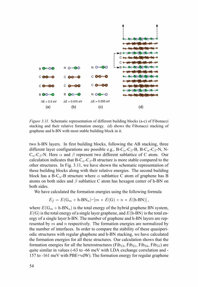
E = 0.0 eV E = 0.015 eV E = 0.055 eV
B B
B
C
C
C
C C
C
NN
N
B
B
C
C
(a) (b) (c) (d)
Figure 3.11. Schematic representation of different building blocks (a-c) of Fibonaccistacking and their relative formation energy. (d) shows the Fibonacci stacking ofgraphene and h-BN with most stable building block in it.
two h-BN layers. In first building blocks, following the AB stacking, threedifferent layer configurations are possible e.g., B-Cα-Cβ-B, B-Cα-Cβ-N, N-Cα-Cβ-N. Here α and β represent two different sublattice of C atom. Ourcalculation indicates that B-Cα-Cβ-B structure is more stable compared to theother structures. In Fig. 3.11, we have shown the schematic representation ofthese building blocks along with their relative energies. The second buildingblock has a B-Cα-B structure where α sublattice C atom of graphene has Batoms on both sides and β sublattice C atom has hexagon center of h-BN onboth sides.
We have calculated the formation energies using the following formula
Ef = E(Gm + h-BNn)−[m ∗ E(G) + n ∗ E(h-BN)] ,
where E(Gm + h-BNn) is the total energy of the hybrid graphene BN system,E(G) is the total energy of a single layer graphene, andE(h-BN) is the total en-ergy of a single layer h-BN. The number of graphene and h-BN layers are rep-resented by m and n respectively. The formation energies are normalized bythe number of interfaces. In order to compare the stability of these quasiperi-odic structures with regular ghaphene and h-BN stacking, we have calculatedthe formation energies for all these structures. Our calculation shows that theformation energies for all the heterostructures (Fib13, Fib21, Fib34, Fib55) arequite similar in values (-63 to -66 meV with LDA exchange correlation and -157 to -161 meV with PBE+vdW). The formation energy for regular graphene
54
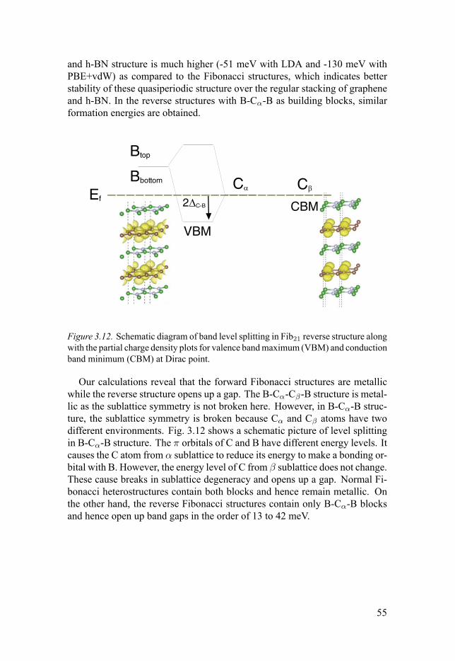
and h-BN structure is much higher (-51 meV with LDA and -130 meV withPBE+vdW) as compared to the Fibonacci structures, which indicates betterstability of these quasiperiodic structure over the regular stacking of grapheneand h-BN. In the reverse structures with B-Cα-B as building blocks, similarformation energies are obtained.
VBM
CBM
Btop
Bbottom
Ef
C C2 C-B
Figure 3.12. Schematic diagram of band level splitting in Fib21 reverse structure alongwith the partial charge density plots for valence band maximum (VBM) and conductionband minimum (CBM) at Dirac point.
Our calculations reveal that the forward Fibonacci structures are metallicwhile the reverse structure opens up a gap. The B-Cα-Cβ-B structure is metal-lic as the sublattice symmetry is not broken here. However, in B-Cα-B struc-ture, the sublattice symmetry is broken because Cα and Cβ atoms have twodifferent environments. Fig. 3.12 shows a schematic picture of level splittingin B-Cα-B structure. The π orbitals of C and B have different energy levels. Itcauses the C atom from α sublattice to reduce its energy to make a bonding or-bital with B. However, the energy level of C from β sublattice does not change.These cause breaks in sublattice degeneracy and opens up a gap. Normal Fi-bonacci heterostructures contain both blocks and hence remain metallic. Onthe other hand, the reverse Fibonacci structures contain only B-Cα-B blocksand hence open up band gaps in the order of 13 to 42 meV.
55


4. The Influence of Defects
“Who in the world am I? Ah, that’s the greatpuzzle.”
— Lewis Carroll, Alice in Wonderland
In this chapter, we will discuss how defects can affect the properties of twodimensional (2D) materials which may some time be beneficial or may sometime be detrimental from the application point of view. The results have beenpresented in Papers V–IX. In the following sections, we will discuss: 1) howvacancy defects affect the adsorption and magnetism of Fe cluster, 2) howvarious defects change the properties of pristine 2D transition metal dichalco-genides, 3) effect of defects in local transport properties in graphene and sil-icene, and 4) how defected graphene can help in gas sensing activities andfluorination of graphene.
We have used VASP [98, 99] code for our electronic structure calculations.For transport calculation we have used the SIESTA [129] code. Finite tempera-ture diffusion of Fe atoms on the 2D sheet was studied using Born-Oppenheimermolecular dynamics (MD). The temperature was controlled using Nosé ther-mostat [130–132].
4.1 Adsorption and magnetism of Fe cluster ongraphene with vacancy defects
The chemical and magnetic interactions of Fen (n=1–6) clusters with vacancydefects (monovacancy to correlated vacancies with six missing C atoms) ingraphene have been presented in paper V. As discussed in the introduction,graphene in particular is prone to the formation of vacancy defects. These va-cancy defects are quite probable to form strong reactive centers [133, 134] andsuch defects can affect the electronic structure and hence transport propertiesof graphene [31, 32]. It is possible to trap magnetic adatoms or clusters atvarious defect sites [133] and a flux of adatoms may generate various sizes ofmagnetic nanoclusters at defect sites.
Another reason for investigating trapping of clusters with ferromagneticspecies, is that for all applications of graphene in spintronics must include a fer-romagnetic spin injector. Regarding spintronic applications, the out-of-planemagnetization has a technological application as it can be used to increase stor-age density. Finite size clusters may act as potential candidate. Another aspect
57

is the spin-dipole contribution, which arises from the anisotropic spin densities.For low dimensional systems, it has a significant role on the effective moment,which is the sum of spin and spin-dipole moments, which can be measured byX-ray magnetic circular dichroism (XMCD) experiments.
Given this background, in this work, we tried to analyze how robust is theformation of clusters on defected sites. The effects of magnetic anisotropy andthe spin-dipole moments under strong Coulomb interaction on these systemsare also discussed.
The ab-initio calculations were performed using PAW method and PBE ex-change correlation functional. The effect of strong electron-electron interac-tions were taken into account using PBE+U method [135], where the Coulombparameter U is added in the Hubbard formalism. For these calculations, wehave used U = 4 eV and the intra-atomic exchange parameter J = 1 eV, whichare typical values for 3d transition metals. [135, 136].
4.1.1 MD resultsIn order to investigate how a number of Fe adatoms placed on a defectedgraphene diffuse, especially whether the Fe adatoms remain isolated or forma cluster, we have performed limited real time Born-Oppenheimer moleculardynamics (MD) up to 30 ps at constant temperature T = 300 K, a tempera-ture expected in most practical applications. We have placed six Fe adatomsat six different sites on the sheet and also removed two adjacent C atoms tocreate a vacancy. Figure 4.1 shows the potential energy landscapes and cor-responding geometries (marked by arrows in figure) at different simulationtimes. The analysis of trajectories and movies of the motion of Fe atoms re-veal interesting observations. At the beginning of the simulation, the C atomsnear the divacancy center come closer and heal the divacancy to form a 585defect (Fig. 4.1(a)). Then the Fe adatoms from the adjacent hexagonal sitescome together and form dimers (Fig. 4.1(b)-Fig. 4.1(d)) in about < 0.7 ps.These dimers come closer to form a cluster (Fig. 4.1(e)-Fig. 4.1(g)). Finally,in the presence of the Fe cluster near the defect, one Fe atom from the clusterforms bond with the C atoms at the defect site and hence breaks the C–C bondsof the pentagonal rings of the 585 defect (Fig. 4.1(h)). Once the cluster getstrapped at the defected site, it remains trapped and only shows thermal oscil-lations till the end of the simulation time. Frequent breaking and forming ofbonds within the Fe cluster and between Fe and C atoms can be seen duringthis time. Fig. 4.1(i), the lowest energy structure obtained from the geometryoptimization after the MD simulation, shows the formation of bonds within Fecluster and between Fe and C atoms. Thus our simulations indicate that theformation of cluster at defected site is fairly robust.
58

(a)
(a)
(b)
(b)
(c)
(c)
(d)
(d)
(e)
(e)
(f)
(f)
(g)
(g)
(h)
(h) (i)
Figure 4.1. Potential energy (P.E.) landscape as a function of simulation time.Schematics (a)-(h) show the snapshots at different simulation times. These snapshotsare also marked by arrow in the P.E. graph. Fig. (i) shows the optimized geometry af-ter the completion of MD simulation for 30 ps. See text in Sec. 4.1.1 for more details.Reproduced with permission from Paper V. Copyright © 2014 American Physical So-ciety.
59

Evac EvacFe
n
1 6
n
2
2
n
n
n n = 1− 6

(a)
(b)
(c)
(d)
(e)
(f)
Figure 4.3. Geometries and spin density of Fen clusters on Vn vacancies (n=1-6) areshown together. Cyan and red balls indicate C and Fe atoms respectively. Yellowand blue isosurface denotes positive and negative spin densities. Reproduced withpermission from Paper V. Copyright © 2014 American Physical Society.
undergo any significant structural rearrangement in presence of Fe clusters.Thus even a single Fe adatom can be used to maintain the structure of underly-ing lattice despite the presence of the vacancy. The geometries of Fe clusterson graphene are remarkably different from those studied in free space [138].As seen from Fig. 4.3(a), the optimized geometry for Fe1 on V1 shows that theminimum energy position for Fe is at the center of the vacancy. The averageFe–C bond length is ∼ 1.77 Å for this case and the height of the Fe adatomfrom the graphene plane is ∼ 1.19 Å. The dimer bond length is about 10 % en-hanced in presence of a divacancy in graphene (see Fig. 4.3(b)) from the bondlength found in a free cluster. The trimer in free space is reported to be anisosceles triangle [138, 139], while the trimer on a vacancy (see Fig. 4.3(c)) isa distorted isosceles triangle with the bond lengths differing substantially fromthat in free space. Fe4 also forms a prism in free space with the bond lengthsranging from 2.22 – 2.41 Å. However in our case the bond length varies sub-stantially from 2.2 Å to 2.63 Å (see Fig. 4.3(d)). The change in the trigonal bipyramid of isolated Fe5 is seen in the vertical four-atom plane where the bondlengths are increased with respect to those in free space (see Fig. 4.3(e)). Fe6undergoes a substantial change from octahedron to a more complex structureseen in Fig. 4.3(f).
In Table 4.1, the adsorption energies for the Fen clusters in a n-vacancygraphene sheet and their magnetic moments are reported, together with themagnetic moments of free Fen clusters. As seen from the Table 4.1, the mag-netic moments of Fe clusters are slightly reduced by their adsorption on then-vacancies except for Fe6 on V6 and Fe1 on V1 where the reduction is huge.However, the magnetic character of the C atoms near to the vacancy is signif-
61

Table 4.1. Adsorption energies EadVn(in eV) for Fen cluster adsorbed in n-vacancy
graphene sheet, together with their magnetic moments (in µB). The calculations aredone within PBE+U formalism. The middle column shows the total moment of a Fecluster on graphene with defects, while the right hand column shows that calculatedmoment for free Fe clusters.Reproduced with permission from Paper V. Copyright ©2014 American Physical Society.
µFenB /n
n EadVn
/n µB/n (Free)
1 5.36 0.32 4.02 2.80 3.00 4.03 2.60 3.32 4.04 2.97 3.00 3.55 2.71 3.20 3.66 2.34 3.33 3.33
icantly affected as seen in Fig. 4.3. The magnetization of the whole system isstill basically due to the Fe adatoms. Except for the case with one Fe adatomon a single vacancy, the average Fe magnetic moments for the adsorbed clus-ters are not so different from the moments in free state. The drastic reductionof magnetic moment for the Fe atom adsorbed at the monovacancy site is dueto a strong hybridization between the Fe–d and C–p orbitals at the defect site.
It can be noted that magnetic moments of the C atoms for the defectedgraphene has reduced significantly after the adsorption of Fe clusters. Theanalysis reveals that Fe atoms induce a substantial number of states on theFermi level and it is seen that those are mainly d-like. This feature is generaland is present in all the clusters. Partially filled in-plane p orbitals of the edgeC atoms around the vacancy sites hybridized with the d-orbitals of adsorbedFe atoms to pacify the dangling bonds and hence, destroy the local momentsat those edge C atoms.
Orbital moments, magnetic anisotropy and spin-dipole momentsWe have included SOC in the Hamiltonian to calculate the orbital momentsand magnetic anisotropy energies (MAEs) for Fen cluster adsorbed systems.Here, MAE corresponds to only magneto-crystalline energy originating fromspin-orbit coupling while the contribution of shape anisotropy is neglected.Table 4.2 shows easy axis, magnetic anisotropy and orbital magnetic momentsalong the easy axes. The calculated average orbital moment of the Fe atomsin these systems are similar to the calculated value for bulk Fe (∼ 0.05 µBwithout orbital polarization) in the bcc phase. It is interesting to note that Fe1and Fe4 clusters exhibit out-of-plane easy axes whereas the other ones haveeasy in-plane magnetization. Therefore, for a flux of adatoms of Fe depositedon graphene defect sites with varieties of cluster formation, one may expectthat the cluster macrospins to lie in the plane or perpendicular to the plane of
62

Table 4.2. MAE-Data with PBE+U , magnetic anisotropy energy (∆E = Ehard −Eeasy), average orbital moment for Fen clusters on n-vacancy graphenes. Repro-duced with permission from Paper V. Copyright © 2014 American Physical Society.
∆E Easy HardCluster ⟨µorb⟩ (meV) axis axis
Fe1 0.010 0.012 (001) (100)Fe2 0.047 0.396 (010) (100)Fe3 0.042 0.843 (010) (100)Fe4 0.032 0.504 (001) (100)Fe5 0.042 0.694 (100) (010)Fe6 0.042 0.708 (100) (001)
graphene. However, one should note that the cluster magnetization directionswill be quite robust as the magnetic anisotropy energies are not so small inmagnitude.
In systems having low symmetry, the contribution of the spin-dipole termis expected to be quite significant. Hence, we have performed DFT calcula-tions to calculate the spin dipole moments, following the method prescribedby Freeman et. al. [140]. In Table 4.3, the values of spin moments ms, spin-dipole moments (7⟨Tz⟩) and effective moments (meff ) are shown. One canclearly see that (i) the spin-dipole contributions are not negligible and (ii) thesigns of 7⟨Tz⟩ are opposite toms in many cases, thereby reducing the effectivemoments of certain Fe atoms in each cluster. The average effective momentvaries non monotonically e.g., the ⟨meff ⟩ are 2.63 µB , 2.65 µB and 3.18 µBfor n = 4 − 6 respectively. In fact, the value of 7⟨Tz⟩ can reach up to 33 %of the spin moment. However, the average effective magnetic moment of thetotal system does not vary much from the average spin moment due to mutualcancellation of atomic 7⟨Tz⟩.
4.2 Atomic-scale defects in 2D transition metaldichalcogenides
The effect of various point defects on the structural, electronic and opticalproperties of transition metal dichalcogenides (TMDs) have been presentedin Paper VI. As discussed in the introduction, 2D TMDs are one of the alter-native “beyond graphene” family members. Unlike graphene, these TMDs aresemiconductors. Defects in general create impurity states into the band gapregion either closer to the valence band (p-type) or closer to the conductionband (n-type). The interaction of localized states from the defects can couplestrongly with the continuum of ionic crystals which have applications in solidstate lasers, white LEDs etc [141].
63
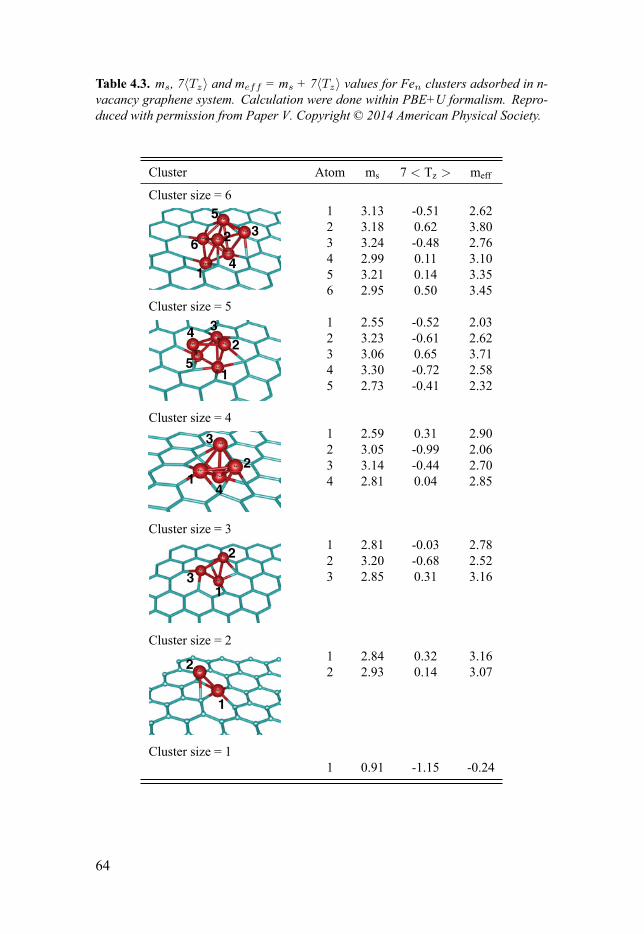
Table 4.3. ms, 7⟨Tz⟩ and meff = ms + 7⟨Tz⟩ values for Fen clusters adsorbed in n-vacancy graphene system. Calculation were done within PBE+U formalism. Repro-duced with permission from Paper V. Copyright © 2014 American Physical Society.
Cluster Atom ms 7 < Tz > meff
Cluster size = 6
4
5
6
1 3.13 -0.51 2.622 3.18 0.62 3.803 3.24 -0.48 2.764 2.99 0.11 3.105 3.21 0.14 3.356 2.95 0.50 3.45
Cluster size = 5
4
5
1 2.55 -0.52 2.032 3.23 -0.61 2.623 3.06 0.65 3.714 3.30 -0.72 2.585 2.73 -0.41 2.32
Cluster size = 4
4
1 2.59 0.31 2.902 3.05 -0.99 2.063 3.14 -0.44 2.704 2.81 0.04 2.85
Cluster size = 31 2.81 -0.03 2.782 3.20 -0.68 2.523 2.85 0.31 3.16
Cluster size = 21 2.84 0.32 3.162 2.93 0.14 3.07
Cluster size = 11 0.91 -1.15 -0.24
64

It is not uncommon to find vacancies during the fabrication process. Forexample MoS2 has been found to acquire S vacancies during fabrication whichcreate deep trap states for electrons [142, 143]. These trap states damage then-type conductivity of MoS2. The mode of fabrication also dictates the amountof defect concentration [144, 145]. There are few theoretical studies availablein the literature where specific defects have been studied [142, 143, 146–153].However systematic studies on the role of various point and double defects onthe electronic and optical properties of TMDs are not available in the literature.Therefore, in this work (Paper VI) we tried to address systematically the roleof defects in electronic and optical properties of MX2 TMDs where M = Mo,W and X = S, Se, Te.
4.2.1 Structure and formation energies
Figure 4.4. Formation energies for different types of defects in various MX2 systemsunder both X–rich and M–rich conditions. Reproduced with permission from PaperVI. Copyright © 2015 American Physical Society.
For our study, we have considered six different type of defects namely X va-cancy, X interstitial, M vacancy, M interstitial, XX vacancy and MX vacancy.We have used various possible configurations of geometry to determine theminimum energy structure for all the systems. We have calculated the forma-
65

tion energies (Ef ) using the following formula:
Ef = Edefect −[Epristine +
∑i
niµi], where
Edefect = total energy of MX2 supercell with defectEpristine = total energy of MX2 supercell without defect
ni = number of i element added or removed (with a negative sign)µi = chemical potential of the element i
We have shown the calculated formation energies under X rich and M rich
ΔL
ΔH X1
X2
X3
X4
X5
a b
c d
e f
Figure 4.5. Representative figure of optimized geometries for various defects in MX2
system as designed on 5×5×1 supercell. (a)–(f) represent the following defects: (a)X interstitial, (b) X vacancy, (c) M vacancy, (d) MX vacancy, (e) XX vacancy and(f) M interstitial. The cyan (large) balls denote the X atoms from the top layer, pink(medium) balls denote M atoms and dark blue (small) balls denote X atoms from thebottom layer. In (a), the purple ball refers the X interstitial atom. In (f), the red ballindicates to the M interstitial atom. Red arrows in (b) indicates the movement of Matoms during the relaxation. ∆L and ∆H in (c) represents the change of in-plane andout-of-plane displacements of the X atoms around the M vacancy due to structuralrelaxation. Reproduced with permission from Paper VI. Copyright © 2015 AmericanPhysical Society.
66

conditions for all the geometries that we have considered in our simulationsin Fig. 4.4. The most stable geometries for X interstitial, X vacancy, M va-cancy, MX vacancy, XX vacancy, and M interstitial defect have been shownin Fig. 4.5 (a)–(f), respectively. The formation energy calculations show thatthe stable X interstitial structure is obtained when the X atom is attached ontop of a host X atom (Fig. 4.5 (a)). X vacancy is created by removing oneX atom from the top X layer. Here, three M atoms surrounding the vacancyrelax towards the vacancy site (Fig. 4.5 (b)). For M vacancy, six X atomswith dangling bonds dictate the relaxation of their geometries near the vacancysite. Outward relaxation from the vacancy center can be observed for S andSe atoms. However, for Te atom, the relaxation occurred towards the vacancycenter (Fig. 4.5 (c)). The energetically favored position for M interstitial de-fects are when the M atom is at the split interstitial position along the c direc-tion except WTe2 (Fig. 4.5 (f)). For WTe2, after relaxation the interstitial Watom settled at hexagonal position in the W layer forming a distorted hexagon.During optimization of MX vacancy, five neighboring X atoms (X1–X5 inFig. 4.5 (d)) nearer to the vacancy site mainly relax. Lowest energy XX diva-cancy structure is obtained when correlated X atoms are removed from the topand bottom layers of X atom (with same x and y coordinates). The M atomsare in general relax towards the vacancy site and form an equilateral triangle(Fig. 4.5 (e)). See Paper VI for details.
4.2.2 Defect concentration at equilibriumIn order to find out the concentration of defects in finite temperature crystalgrowth condition, we have also calculated the equilibrium defect concentrationusing the following formula,
Ceq = Ne−Ef/kBT
where N is the concentration of possible defect sites, Ef is the zero tempera-ture formation energy of the defect and T is the temperature. We have chosenT= 1000 K – 1200 K during the crystal growth. This range of temperatureis chosen as most of the MX2 single layer structures are synthesized experi-mentally in this range [154–159]. From our calculation, it is quite evident thatunder X rich condition, X interstitial defects and underM rich condition, X va-cancy defects will occur more frequently. However, the probability of formingM interstitial or M vacancies are quite low.
4.2.3 Electronic structure and optical propertiesEnergy level diagrams for all six defects in all MX2 system have been con-structed and shown in Fig. 4.6. The columns (a)–(f) in each subplot indicates
67

Mo
S
W
a b c d e f
VBM
CBM
a b c d e f
VBM
CBM
Se
a b c d e f
VBM
CBM
a b c d e f
VBM
CBM
a b c d e f
VBM
CBM
Te
a b c d e f
VBM
CBM
Figure 4.6. Energy level diagram for different defects in all the MX2 systems. In eachsubplot, columns (a)-(f) refer to X interstitial, X vacancy,M vacancy,MX vacancy, XXvacancy and M interstitial respectively. The orange (long dashed in print) line showsthe position of VBM and CBM for pristine MX2. Green solid and dashed lines denotethe occupied and unoccupied defect states respectively. Reproduced with permissionfrom Paper VI. Copyright © 2015 American Physical Society.
X interstitial, X vacancy, M vacancy, MX vacancy, XX vacancy, and M in-terstitial defect, respectively. The position of conduction band minima (CBM)and valence band maxima (VBM) were marked using an orange dashed line.The green solid and dashed line represents the position of defect states in occu-pied and unoccupied states, respectively. Density of states (DOSs) calculationindicates that the qualitative nature of DOSs are quite similar between MoS2,WS2; MoSe2 , WSe2; and MoTe2, WTe2. Our analysis of energy level diagram(see Fig. 4.6) and DOSs indicate that in general defect states appear in the bandgap region of the pure system except for X interstitial defects. In case of X in-terstitial defects, the impurity states appear near the band edges and merge withboth valence and conduction bands.
Defects in the MX2 can also cause changes in the optical properties. How-ever, our calculations indicate that the most notable change can be visible forthe following three defects: - i)M vacancy, ii) X vacancy and iii)MX vacancy.Therefore we have shown optical spectra for the three defects in MoX2 sys-tem in Fig. 4.7. For Mo vacancy in MoS2, defect peaks occur below and abovethe Fermi energy giving rise to a transition around 1 eV. The peak in MoSe2 isbroader due to the fact that there are two possible transitions within a very closeenergy range. In MoTe2, the defect state due to Mo vacancy occurs very closeto the Fermi energy and therefore generates a sharp optical transition at a very
68

MoS2
2
4
6
8
10
ε2
(Arb
. u
nit)
Figure 4.7. Comparison of imaginary parts of the dielectric functions (ε2) betweenMoS2, MoSe2, and MoTe2 for M vacancy, X vacancy, and MX vacancy. Blue andorange lines denote in-plane contribution of ε2 for defected and pure systems, respec-tively. Purple and green lines denote out-of-plane contribution of ε2 for defected andpure systems, respectively. The shaded region represents the prominent contributionsof defect related peaks compared to the pristine system. Reproduced with permissionfrom Paper VI. Copyright © 2015 American Physical Society.
low energy. For X vacancies, defect states are closer to conduction band min-imum and hence the optical spectra show slight changes from pristine. Thereare number of defect peaks appearing near the Fermi energy for MX vacancyand hence transition occurs at around 0.5 eV, which shows a broader peakcompared to the M vacancy. For MX2 systems, the absorption spectra occurin the visible region which can be suitable for photocatalysis using sunlight.Optical properties for the above three defects show similar characteristics forWX2 systems.
4.3 Electronic transport properties of graphene andsilicene with defects
As we have discussed before, silicene (a 2D sheet of Silicon) can be a viablealternative to graphene. Silicene has hexagonal structure and its electronic
69
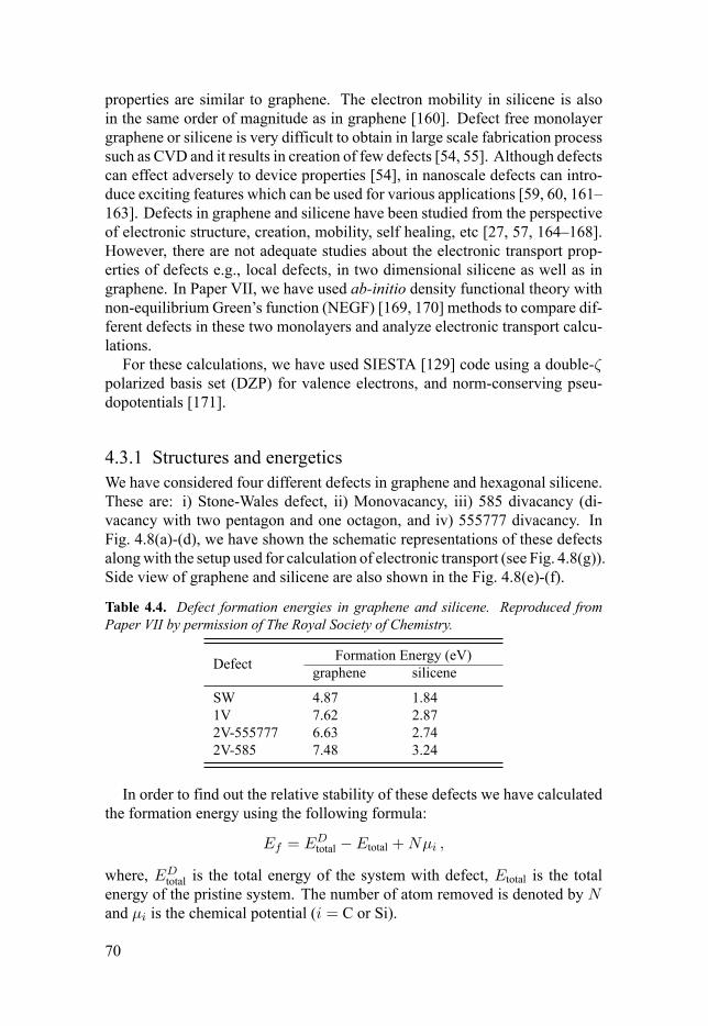
properties are similar to graphene. The electron mobility in silicene is alsoin the same order of magnitude as in graphene [160]. Defect free monolayergraphene or silicene is very difficult to obtain in large scale fabrication processsuch as CVD and it results in creation of few defects [54, 55]. Although defectscan effect adversely to device properties [54], in nanoscale defects can intro-duce exciting features which can be used for various applications [59, 60, 161–163]. Defects in graphene and silicene have been studied from the perspectiveof electronic structure, creation, mobility, self healing, etc [27, 57, 164–168].However, there are not adequate studies about the electronic transport prop-erties of defects e.g., local defects, in two dimensional silicene as well as ingraphene. In Paper VII, we have used ab-initio density functional theory withnon-equilibrium Green’s function (NEGF) [169, 170] methods to compare dif-ferent defects in these two monolayers and analyze electronic transport calcu-lations.
For these calculations, we have used SIESTA [129] code using a double-ζpolarized basis set (DZP) for valence electrons, and norm-conserving pseu-dopotentials [171].
4.3.1 Structures and energeticsWe have considered four different defects in graphene and hexagonal silicene.These are: i) Stone-Wales defect, ii) Monovacancy, iii) 585 divacancy (di-vacancy with two pentagon and one octagon, and iv) 555777 divacancy. InFig. 4.8(a)-(d), we have shown the schematic representations of these defectsalong with the setup used for calculation of electronic transport (see Fig. 4.8(g)).Side view of graphene and silicene are also shown in the Fig. 4.8(e)-(f).
Table 4.4. Defect formation energies in graphene and silicene. Reproduced fromPaper VII by permission of The Royal Society of Chemistry.
Defect Formation Energy (eV)graphene silicene
SW 4.87 1.841V 7.62 2.872V-555777 6.63 2.742V-585 7.48 3.24
In order to find out the relative stability of these defects we have calculatedthe formation energy using the following formula:
Ef = EDtotal − Etotal +Nµi ,
where, EDtotal is the total energy of the system with defect, Etotal is the total
energy of the pristine system. The number of atom removed is denoted by Nand µi is the chemical potential (i = C or Si).
70
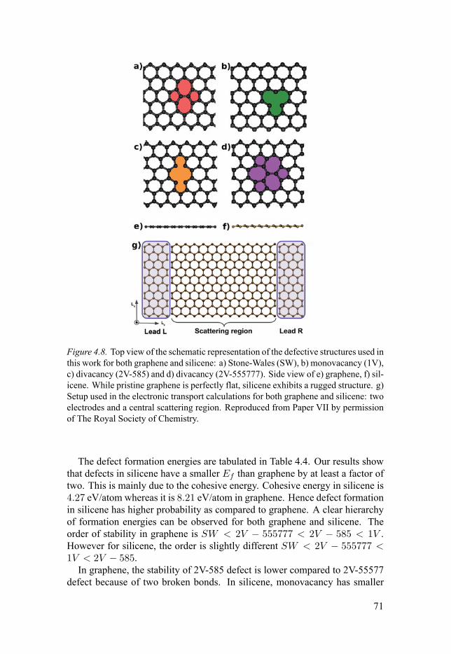
Figure 4.8. Top view of the schematic representation of the defective structures used inthis work for both graphene and silicene: a) Stone-Wales (SW), b) monovacancy (1V),c) divacancy (2V-585) and d) divacancy (2V-555777). Side view of e) graphene, f) sil-icene. While pristine graphene is perfectly flat, silicene exhibits a rugged structure. g)Setup used in the electronic transport calculations for both graphene and silicene: twoelectrodes and a central scattering region. Reproduced from Paper VII by permissionof The Royal Society of Chemistry.
The defect formation energies are tabulated in Table 4.4. Our results showthat defects in silicene have a smaller Ef than graphene by at least a factor oftwo. This is mainly due to the cohesive energy. Cohesive energy in silicene is4.27 eV/atom whereas it is 8.21 eV/atom in graphene. Hence defect formationin silicene has higher probability as compared to graphene. A clear hierarchyof formation energies can be observed for both graphene and silicene. Theorder of stability in graphene is SW < 2V − 555777 < 2V − 585 < 1V .However for silicene, the order is slightly different SW < 2V − 555777 <1V < 2V − 585.
In graphene, the stability of 2V-585 defect is lower compared to 2V-55577defect because of two broken bonds. In silicene, monovacancy has smaller
71

formation energy than 2V-585 defect. However, in graphene, the trend is op-posite. The reason behind this is that the buckling in silicene helps for bet-ter rearrangement of dangling bonds in monovacancy compared to graphene.This is also evident in the value of magnetic moment. While monovacancy ingraphene shows a 1.4 µB magnetic moment, monovacancy in silicene showszero magnetic moment.
4.3.2 Transport properties
Figure 4.9. Transmission coefficients as a function of energy for the different defects ina) graphene, and b) silicene. The insets show a zoom-in of the region around the Diraccone. Reproduced from Paper VII by permission of The Royal Society of Chemistry.
We have calculated the transverse electronic transport properties of siliceneand graphene and compared them with the pristine system. By applying a com-
72
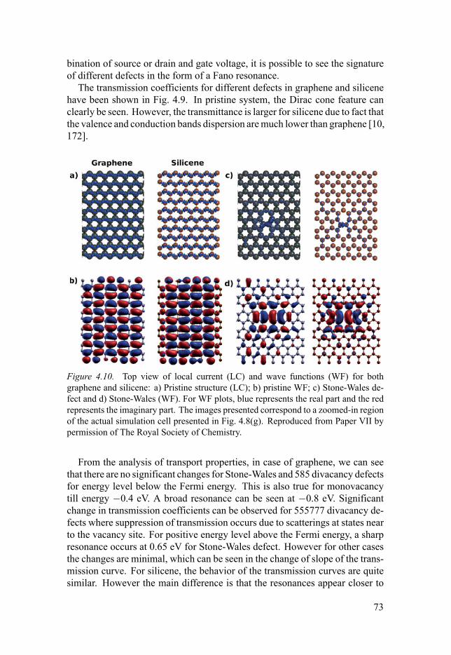
bination of source or drain and gate voltage, it is possible to see the signatureof different defects in the form of a Fano resonance.
The transmission coefficients for different defects in graphene and silicenehave been shown in Fig. 4.9. In pristine system, the Dirac cone feature canclearly be seen. However, the transmittance is larger for silicene due to fact thatthe valence and conduction bands dispersion are much lower than graphene [10,172].
Figure 4.10. Top view of local current (LC) and wave functions (WF) for bothgraphene and silicene: a) Pristine structure (LC); b) pristine WF; c) Stone-Wales de-fect and d) Stone-Wales (WF). For WF plots, blue represents the real part and the redrepresents the imaginary part. The images presented correspond to a zoomed-in regionof the actual simulation cell presented in Fig. 4.8(g). Reproduced from Paper VII bypermission of The Royal Society of Chemistry.
From the analysis of transport properties, in case of graphene, we can seethat there are no significant changes for Stone-Wales and 585 divacancy defectsfor energy level below the Fermi energy. This is also true for monovacancytill energy −0.4 eV. A broad resonance can be seen at −0.8 eV. Significantchange in transmission coefficients can be observed for 555777 divacancy de-fects where suppression of transmission occurs due to scatterings at states nearto the vacancy site. For positive energy level above the Fermi energy, a sharpresonance occurs at 0.65 eV for Stone-Wales defect. However for other casesthe changes are minimal, which can be seen in the change of slope of the trans-mission curve. For silicene, the behavior of the transmission curves are quitesimilar. However the main difference is that the resonances appear closer to
73
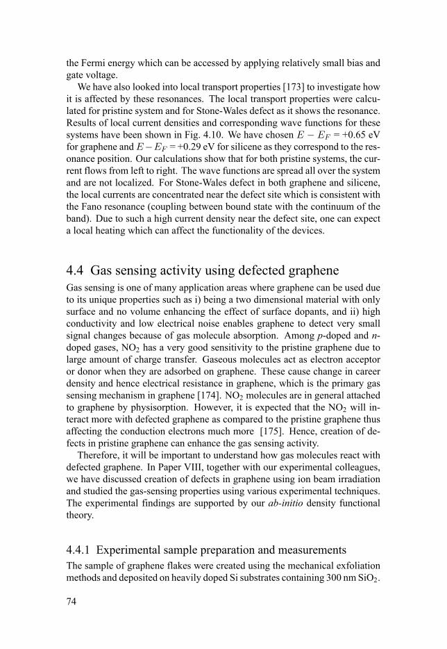
the Fermi energy which can be accessed by applying relatively small bias andgate voltage.
We have also looked into local transport properties [173] to investigate howit is affected by these resonances. The local transport properties were calcu-lated for pristine system and for Stone-Wales defect as it shows the resonance.Results of local current densities and corresponding wave functions for thesesystems have been shown in Fig. 4.10. We have chosen E − EF = +0.65 eVfor graphene andE−EF = +0.29 eV for silicene as they correspond to the res-onance position. Our calculations show that for both pristine systems, the cur-rent flows from left to right. The wave functions are spread all over the systemand are not localized. For Stone-Wales defect in both graphene and silicene,the local currents are concentrated near the defect site which is consistent withthe Fano resonance (coupling between bound state with the continuum of theband). Due to such a high current density near the defect site, one can expecta local heating which can affect the functionality of the devices.
4.4 Gas sensing activity using defected grapheneGas sensing is one of many application areas where graphene can be used dueto its unique properties such as i) being a two dimensional material with onlysurface and no volume enhancing the effect of surface dopants, and ii) highconductivity and low electrical noise enables graphene to detect very smallsignal changes because of gas molecule absorption. Among p-doped and n-doped gases, NO2 has a very good sensitivity to the pristine graphene due tolarge amount of charge transfer. Gaseous molecules act as electron acceptoror donor when they are adsorbed on graphene. These cause change in careerdensity and hence electrical resistance in graphene, which is the primary gassensing mechanism in graphene [174]. NO2 molecules are in general attachedto graphene by physisorption. However, it is expected that the NO2 will in-teract more with defected graphene as compared to the pristine graphene thusaffecting the conduction electrons much more [175]. Hence, creation of de-fects in pristine graphene can enhance the gas sensing activity.
Therefore, it will be important to understand how gas molecules react withdefected graphene. In Paper VIII, together with our experimental colleagues,we have discussed creation of defects in graphene using ion beam irradiationand studied the gas-sensing properties using various experimental techniques.The experimental findings are supported by our ab-initio density functionaltheory.
4.4.1 Experimental sample preparation and measurementsThe sample of graphene flakes were created using the mechanical exfoliationmethods and deposited on heavily doped Si substrates containing 300 nm SiO2.
74

+
∼ −6∼ 12 −2 20× μ 2
∼ 12 −2
0
∼ −1 ∼−1
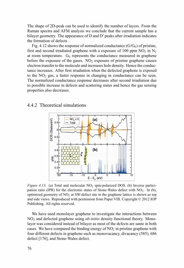
′
0
0

Table 4.5. Binding energies for NO2 molecules on pristine and defected graphene.Reproduced with permission from Paper VIII. Copyright © 2012 IOP Publishing. Allrights reserved.
Structure EB (eV)
Pristine 0.30Monovacancy 0.32Divacancy (585) 0.28686 Defect 0.35Stone-Wales 0.72
In Table 4.5, we have tabulated the binding energies of NO2 molecule withpristine graphene and other defects. Our calculations indicate that the NO2molecule binds strongly with the Stone-Wales defect with binding energy valueof 0.72 eV. In other defects, the binding energies are ∼ 0.3 eV.
The total density of states along with the site projected density of statesfor NO2 are shown in Fig. 4.13. The spin polarized molecular levels of NO2molecules appear near the Fermi energy causing 1 µB / cell magnetic moment.We have also calculated inverse participation ratio (IPR) [177] for the elec-tronic states of NO2 adsorbed Stone-Wales defect (see Fig. 4.13(b)). IPR isinversely proportional to the number of atoms that are contributing to a spe-cific molecular orbital. Hence a quantitative description of molecular orbitallocalization can be given from IPR. In our calculation, the IPR has very smallvalues near the Fermi energy indicating a conducting character of the states.
The binding energy and sticking probability for NO2 molecules on a pristineand defected graphene surface are further analyzed using Langmuir isothermmodel. Our results show that higher binding energies are required in orderto explain experimental rise time. Our DFT calculation correctly predicts in-crease of binding energy for Stone-Wales defect which results into a increasedadsorption and conductivity.
4.5 Site-selective local fluorination of graphene withdefects
Functionalization of graphene is one of many routes to make graphene ad-vantageous for application purpose. Local approach in functionalization isan up-and-coming method to retain the beneficial properties of graphene afterits modification of structure and functionalization. Among various possibili-ties, functionalization by using plasmas containing radicals is quite promising.Plasma enhanced graphene functionalizations have been shown in various ex-periments [178–181]. However, these methods are not selective to the localsites and extra photo/electron resist has to be used which can cause unwanted
77

impurities on the surface of graphene. In Paper IX, we have reported a uniqueapproach which allows a precise site-selective fluorination of graphene. Theexperimental results are supported by the ab-initio density functional theorybased simulations.
4.5.1 Sample preparations and experimental results
Figure 4.14. Characterization of pristine graphene, defected graphene (DG) and fluo-rinated graphene (FG). (a) Scanning electron microscope (SEM) image of local func-tionalization of graphene (100 µm × 100 µm) with ion doses of 1013 ions/cm2 andsimultaneous 167s gas exposure. (b) Scanning tunneling microscopy image of DGunder the same ion dosage. (c) X-ray photoelectron spectroscopy spectra of F 1s peakof pristine graphene, DG and FG. FG reveals a distinguished F 1s peak, and the F1s spectrum of pristine graphene as well as DG is given as a reference. (d) Ramancomparison of pristine graphene, DG and FG. Lower ID/IG in FG in contrast to DGindicates lower degree of defects density and larger crystalline size. Reprinted fromPaper IX.
In order to fluorinate graphene (FG), we have used focused ion beam (30kVGa+) irradiation dosage of 1013 ions/cm2 with exposure to XeF2 for 167s. Forcomparison purpose, defected graphene (DG) has been prepared using onlyion irradiation. The basic principle of this type of fluorination process is tocreate reaction between fluorine contained molecules and defected graphene
78

containing carbon atoms with dangling bonds. We have used 100 µm × 100µm area for the irradiation purpose (see Fig. 4.14(a)). Fig. 4.14(b) shows thescanning tunneling image of DG structure prepared using same ion irradiationdosage. Under this amount of dose, most of the lattice structures of grapheneremains intact. However, defects in terms of vacancies form in the damagedpart of the graphene. Distinct XPS peak for F 1s can be seen in FG whichindicates its formation. The intensity of F 1s peak increases for grazing anglesignifying the surface localization of fluorine atoms.
Structural information can also be obtained from the Raman spectroscopy(see Fig. 4.14(d)). The analysis of Raman spectra shows that after irradia-tion the intensity of D-peak (at 1350 cm−1), which is negligible in pristinegraphene, increases. However, there is a drastic decrease in the intensity of2D-peak (at 2700 cm−1) indicating the breaking of translational symmetry ofthe sp2 carbon bonds in graphene. The ratio of D-peak and G-peak (ID/IG) islower in FG as compared to the DG which indicates lesser number of structuraldisorder in FG. To analyze and understand the structures in more details, STMcalculation were performed on FG sample which indicates that the fluorineatoms are localized near to the defects created by irradiation.
4.5.2 Fluorination of graphene from materials modeling
Table 4.6. Adsorption energies of fluorine on pristine graphene as well as the edgecarbon atoms surrounding defects. Reprinted from Paper IX.
Structure Eabs (eV) Hybridization
Pristine -1.91 sp3
Divacancy site A -2.86 sp3
Divacancy site B -2.25 sp3
Hole defect site C (dangling bond) -5.64 sp2
Hole defect site D -2.18 sp3
In order to investigate the adsorption behavior of fluorine atoms on defectedgraphene, we have performed ab-initio density functional theory calculations.Following the STM experiments, we have considered two different type of de-fects to model our simulations. These two models are – i) divacancy modeland ii) hole-defect model which are shown in Fig. 4.15. There are four differ-ent possible places (marked as site A–D) where a single fluorine atom can beadsorbed. In Table 4.6 we have tabulated the adsorption energies for fluorineatom in these four sites. From the Table 4.6, it can be clearly seen that theadsorption energies for fluorine atom are quite lower around the defected sitesas compared to the pristine graphene. It suggest that fluorine atoms are moreprone to react with the carbon atoms surrounding the defect sites. At site C,due to the presence of dangling bond at the carbon atom, the adsorption energy
79

Figure 4.15. Ab-initio density functional calculation models of fluorinated graphene.Di-vacancy model (a) and hole-defect model (b), 0.95 nm in length, are based on theSTM observations. Adsorption energies are shown in table 4.6. Reprinted from Pa-per IX.
of fluorine at this site is much lower compare to others. Here the carbon flu-orine bond length is 1.36 Å, which is typical for a sp2 hybridization and thisbond has in-plane orientation. In other adsorption sites a sp3 hybridization canbe observed.
80

Part III:Final Conclusions


5. Summary and Outlook
“Would you tell me, please, which way I oughtto go from here?”“That depends a good deal on where you wantto get to,” said the Cat.
— Lewis Carroll, Alice in Wonderland
The material research to find out suitable materials for beyond silicon elec-tronics has become a predominant part in various aspects of science and tech-nology in the 21st century. Graphene and other “beyond graphene” familyof materials are among the many promising candidates in this regard. How-ever, it is experimentally challenging to produce these materials in large scalequantity without incorporating any defects or impurities. From the device fab-rication point of view, these defects or impurities can be either beneficial e.g.,modification of material properties to get a desired outcome, or detrimentale.g., creating scattering states in electronic current transport. Hence, a properunderstanding of the repercussions caused by these impurities and defects onthese materials is extremely important. Therefore, the research work carriedout in this thesis was focused on the effects of impurities and defects in modify-ing the properties of graphene and its derivatives, silicene and transition metaldichalcogenides for applications ranging from solar cells, nanoelectronics, op-toelectronics, gas sensors, spintronics, etc.
We have mainly focused on the results of metallic impurities in grapheneand its derivative structures in Chapter 3. We have also looked into the proper-ties of quasiperiodic graphene and hexagonal boron nitride hybrid heterostruc-ture systems to solve the classic band gap problem of graphene. In Chapter 4,we have discussed how defects affect the properties of graphene, silicene andtransition metal dichalcogenides. Paying attention to spintronics and magneticdevice applications, we have used single or small nanostructures of Fe as ourchoice of transition metal impurities.
In our study of single and a pair of Fe atoms in graphene/graphane interfacestructures shows that the responses of the magnetic impurities are different in“armchair” and “zigzag” channels. While the magnetic response is localizedin the armchair channel, it is delocalized in the zigzag channel. An in-planeeasy axis with relatively large magnetic anisotropy energy can be observed inthe armchair channel. The Fe atoms strongly interact with the zigzag chan-nel and hence a stronger ferromagnetic coupling between the the Fe atoms can
83
be observed. A possibility of realizing a spin gapless semiconductor mate-rial by doping appropriate magnetic impurities have been observed in the arm-chair channel. In the conducting zigzag channel, magnetic interaction betweentwo impurities shows oscillating coupling across the edge for a specific width.Hence, a possibility of creating ultrathin device with fascinating properties hasbeen discussed.
In our study of reconstructed zigzag graphene nanoribbons, we have shownthat the reconstructed zigzag edges behave as metal and it does not show anymagnetism. Using single and double hydrogen atoms, chemical functional-ization of the edges are possible. However, the functionalization using twohydrogen atoms are preferable than the one. To introduce magnetism, we havealso functionalize the edges with Fe chains which shows a variation of interedge magnetic coupling between ferromagnetic and antiferromagnetic.
From the study of diffusion of Fe nanostructures on 2D hybrid structures ofgraphene and h–BN, we have shown that the diffusion barriers have smallervalues on the h–BN part as compare to those in graphene part. Using in-depthab-initio molecular dynamics simulations at room temperature (300 K), weconclude that mobile Fe adatoms form Fe clusters and they are eventually set-tled at the C–B interface. We predict that the artificially designed 2D hybrids ofgraphene and h–BN may act as potential substrates for spontaneous formationof magnetic structures at C–B interfaces.
We have also studied the properties of 3D quasiperiodic arrangements ofgrpahene and hexagonal boron nitride and demonstrated that these arrange-ments are more stable than their counterpart 1:1 periodic arrangement. Wehave shown that an opening of band gap is possible using certain sequences ofFibonacci stacking.
We have also shown that in pure graphene, the formation of correlated va-cancy is facilitated. Molecular dynamics study revealed that the adsorbed Feadatoms form clusters in a very short time scale and get trapped at the vacancysites. It is also observed that the Fe clusters promote vacancy formation, i. e., itbecomes easier to remove C atoms from the graphene lattice in presence of Fe.The strong adsorption of Fe clusters at the vacancy sites produces anisotropyin geometries and spin densities. Hence, a strong variation of local spin-dipolemoments (parallel or antiparallel to the spin moments) yields a significant vari-ation in the effective moments, which are measurable in XMCD experiments.The analyses of magnetic anisotropy energies reveal that for some of the clustersizes, out-of-plane easy axes of magnetization are stabilized with a moderatelylarge MAE, which could be important for magnetic data storage.
In our extensive study of native defects in transitional metal dichalcogenides(MX2; M=Mo, W; X=S, Se, Te) we have found out that X interstitial defect isthe most probable defects that will form under X rich conditions. However,under M rich environment, X vacancy is the energetically most favored de-fect except MTe2 systems. M atom related defects have in general quite highformation energy leading to the formation of these defects inMX2 systems un-
84
likely. These defect states appear in the gap region in general and suitablydesigned defected systems can be a good source for making light emitting de-vices.
Analysis of defect formation energies in graphene and silicene indicate thatthe formation of defects will be much easier in the latter material. STM simu-lations indicate that it will be difficult to distinguish defects in buckled silicenestructure using STM and measuring I−V characteristics can be a way around.Presence of these defects causes scattering leading to increment of local currentdensities which can cause heating and possible deterioration in device perfor-mance.
Our experiments and theoretical simulations confirm that the gaseous NO2molecule bind strongly with defected graphene which in turn increases the sen-sitivity of graphene to NO2 gas molecule with a factor of three. Hence wespeculate that defected graphene will be a very good candidate for gas sens-ing purpose. Deliberate creation of defects using ion bombardment can alsofacilitate the local site selective functionalization of graphene with Fluorineatoms.
5.1 Future prospectsThe computational techniques that I have learned during my Ph. D can beused to investigate various other interesting properties of graphene and other2D materials. Graphene has been called “wonder material” after its experi-mental realization in 2004. Since then, a tremendous effort has been put ingraphene research to use these 2D materials in commercial products. Despitethat, it remains challenging to use graphene in large commercial quantities.Recently, Briggs Automotive Company launched a new model of car called“Mono” with panels made out of graphene. But, still in 2016 and in comingyears the research and prototype phase of graphene will continue. It may takedecades to make graphene a commercial success. Hence, the research on 2Dmaterials has become a rapidly increasing field. There are almost 40 possi-ble transition metal dichalcogenides (TMDs) possible as depicted in Fig. 5.1.However, There are other 2D materials like silicene, phosphorene, etc., whichhave various interesting properties. Hybrid 2D planar or 3D heterostructuresusing various TMDs and other 2D materials are also becoming quite promisingin this regard.
One of the major issues that the 2D materials researches are facing is toproduce large defect free materials in a cost effective way. Hence understand-ing of these vast number 2D pristine systems as well as systems with variousdefects and impurities such as line defects, grain boundaries, etc. are quiteimportant. As a future project, I want to continue my research in the field of2D materials keeping in mind various applications oriented goal. The realiza-tion of practical devices relies on understanding of electron transport in these
85
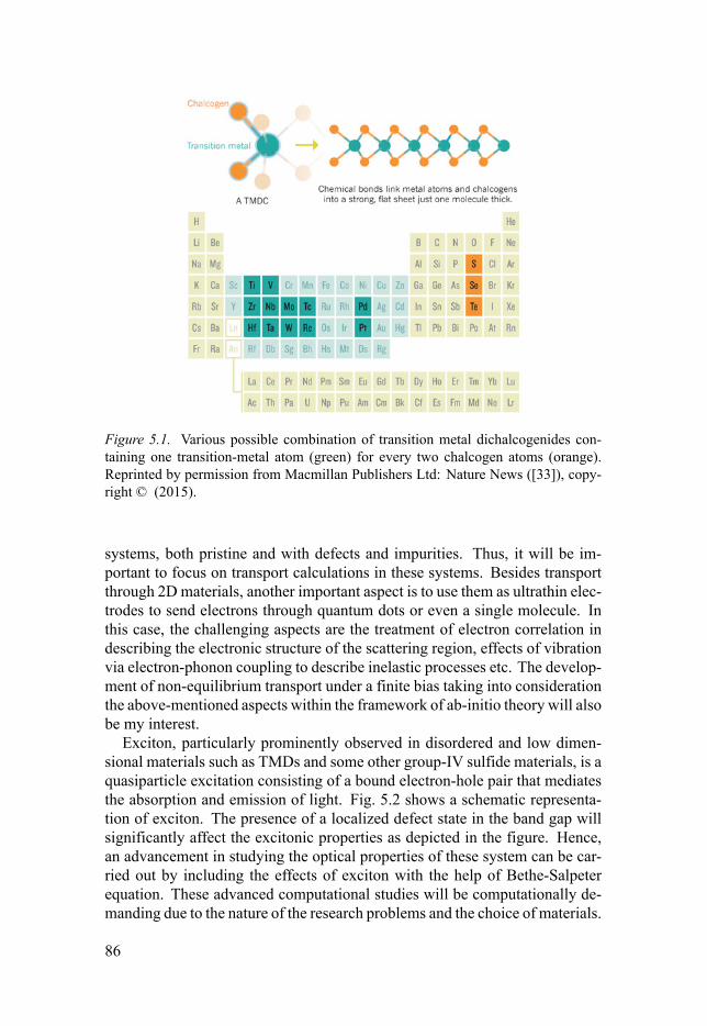
Figure 5.1. Various possible combination of transition metal dichalcogenides con-taining one transition-metal atom (green) for every two chalcogen atoms (orange).Reprinted by permission from Macmillan Publishers Ltd: Nature News ([33]), copy-right © (2015).
systems, both pristine and with defects and impurities. Thus, it will be im-portant to focus on transport calculations in these systems. Besides transportthrough 2D materials, another important aspect is to use them as ultrathin elec-trodes to send electrons through quantum dots or even a single molecule. Inthis case, the challenging aspects are the treatment of electron correlation indescribing the electronic structure of the scattering region, effects of vibrationvia electron-phonon coupling to describe inelastic processes etc. The develop-ment of non-equilibrium transport under a finite bias taking into considerationthe above-mentioned aspects within the framework of ab-initio theory will alsobe my interest.
Exciton, particularly prominently observed in disordered and low dimen-sional materials such as TMDs and some other group-IV sulfide materials, is aquasiparticle excitation consisting of a bound electron-hole pair that mediatesthe absorption and emission of light. Fig. 5.2 shows a schematic representa-tion of exciton. The presence of a localized defect state in the band gap willsignificantly affect the excitonic properties as depicted in the figure. Hence,an advancement in studying the optical properties of these system can be car-ried out by including the effects of exciton with the help of Bethe-Salpeterequation. These advanced computational studies will be computationally de-manding due to the nature of the research problems and the choice of materials.
86
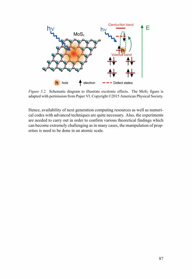
Figure 5.2. Schematic diagram to illustrate excitonic effects. The MoS2 figure isadapted with permission from Paper VI. Copyright ©2015 American Physical Society.
Hence, availability of next generation computing resources as well as numeri-cal codes with advanced techniques are quite necessary. Also, the experimentsare needed to carry out in order to confirm various theoretical findings whichcan become extremely challenging as in many cases, the manipulation of prop-erties is need to be done in an atomic scale.
87


6. Populärvetenskaplig sammanfattning
Elektronik, ett område inom vetenskap och teknik, behandlar elektroniska ap-parater tillverkade av olika elektriska komponenter, t.ex. vakuumrör, dioder,transistorer, integrerade kretsar (IC), etc. Elektronikuppfinningarnas histo-ria sträcker sig tillbaks till 1745, då Kleist och Musschenbroek först uppfann“Leydenflaskan”, vilken var den ursprungliga kondensatorn. Sedan dess harolika uppfinningar och upptäckter byggt en solid grund för utvecklingen avelektronik. Flemings upptäckt av dioden 1905 utlöste början av den modernatidens starka präglan av elektroniken. Dioder och vakuumrör blev integreradedelar inom elektroniken under den tidiga delen av 20-talet och uppfinningenav dessa vakuumrör har gjort teknik så som radio, TV, telefonnät, datorer, etc.mycket populära och utbredda. Men användningen av vakuumrör gjorde dessatekniker kostsamma och anordningarna skrymmande.
Miniatyrisering av moderna elektroniska apparater har alltid fascinerat män-niskor i allmänhet. De halvledarkomponenter som uppfanns under 1940-taletgjorde det möjligt att tillverka mindre, mer hållbara, billigare och effektivarefasta-tillsånds enheter än vakuumrör. Därför började dessa fasta-tillsånds en-heter, så som transistorer, gradvis att ersätta vakumrören på 1950-talet. I jak-ten på mindre storlek upfanns integrerade kretsar (IC). Möjligheten att min-ska storleken för dagens moderna elektroniska apparater är starkt beroend avmöjligheten att minska storleken hos dessa integrerade kretsarna (IC), vilka ärderas hjärtan och hjärnor.
Kiselbaserade integrerade kretsar har begränsningar för hur små de kan gör-as. Strävan efter nya material och tekniker som har möjlighet att ersätta kiselpågår därför redan. Bland flera andra alternativ har grafen, vilket består avett tvådimensionellt (2D) monolager av kolatomer ordnade i ett hexagonaltgitter, blivit det mest lovande. Men även om grafen har några extraordinäraegenskaper så gjorde avsaknaden av ett bandgap grafen olämpliga för transis-torapplikationer. Detta har lett forskare till att leta efter andra 2D-material medlämpliga egenskaper där ström genom materialet kan slås “PÅ” och “AV”. Bild-andet av defekter och föroreningar i dessa 2D-material är en del av tillverkn-ingsprocessen och kan inte undvikas. Dessa defekter och föroreningar påverkaregenskaperna hos dessa material. Å ena sidan kan dessa defekter och förorenin-gar förstöra elektriska egenskaper, å andra sidan kan de på nanoskala intro-ducera nya egenskaper som kan vara till nytta för att skapa enheter för olikatillämpningar. Följaktligen måste det undersökas grundligt hur dessa defekteroch föroreningar påverkar egenskaperna hos dessa material.
89

I denna avhandling har vi diskuterat effekten av föroreningar och defekterpå grafen och andra 2D-material. Vi har använt ab-initio täthetsfunktionalte-oribaserade datorsimuleringar för att analysera de strukturella och elektron-iska egenskaperna hos dessa system. Bortsett från 2D material så som grafen,silicene och övergångsmetalldichalcogenides (TMDC) har vi använt både 2Doch 3D hybridstrukturer som härstammar från 2D material. Olika 2D mate-rial så som grafen, hydrerad grafen(grafan) och hexagonal bornitrid (h-BN)är antingen staplade i 3D eller 2D för att bilda dessa hybridstrukturer. Somorenhet har vi i vår studie studerat en enstaka järnatom eller en grupp av jär-natomer. Hybridstrukturer av grafen-grafan kan likna grafennanoband och visarintressanta magnetiska egenskaper i närvaro av järnföroreningar. Med hjälp avkantrekonstruktion kan sicksacks-grafennanoband visa kantmetallicitet. 2D-(plana) och 3D-hybridstrukturer av grafen och h-BN visar också intressantaegenskaper. Öppnande av bandgap är möjligt med hjälp av vissa specifika ar-rangemang av 3D kvasiperiodisk stapling av grafen och h-BN, och dessa struk-turer är mer stabila än normalt återkommande stapling. Plana hybridstrukturerkan fånga järnkluster på kol-bor-gränssnitt och därmed kan dessa strukturerfungera som potentiella substratmaterial för att bilda magnetiska nanostruk-turer.
Vakanserna i grafen föredrar att bildas på ett korrelerat sätt vilket underlät-tar adsorption av föroreningsatomer så som järnatomer, vilka tenderar att bildakluster som fastna på de vakanta platserna. Detta är i motsats till den mycketdiffusiva situationen på rent grafen och därmed kan dessa magnetiska enhetertillhandahålla stabila magnetiska moment som är användbara för att lagra in-formation.
Tillsammans med experimentalister har vi etablerat att defekter i grafenäven hjälper med platsselektiv lokal fluorering och adsorption av gasformigtNO2. Skapandet av defekter i grafen ökar NO2 känsligheten hos grafen ochsålunda kommer det att vara användbart som en gaskänslig anordning. Ävenom defekter kan hjälpa i vissa tillämpningar så visar våra elektroniska trans-portberäkningar att defekter även kommer leda till spridning. Denna spridningkommer att leda till en ökning i lokal ström och värme, vilket kan leda tillförsämrad prestanda för enheter. I vår systematiska studie av olika defekter iolika TMDCs har vi visat att defektsignaturer lätt kan ses i strukturella, elek-troniska och optiska egenskaper.
I ett nötskal diskuterar denna avhandling olika aspekter av orenheter och de-fekter i grafen och relaterade 2D-material. Vi har diskuterat hur dessa antingenkan vara skadliga eller till nytta i olika enhetsapplikationer. I framtiden vill viytterligare utöka våra studier för att studera effekterna av linjedefekter, korn-gränser i TMDCs. Ett annat intressant ämne skulle vara att studera excitoner,som är bundna tillstånd av elektroner och hål, och deras signaturer i det optiskaspektrumet i närvaron av lokala defekter.
90

Acknowledgments
“Knowledge is in the end based onacknowledgment.”
— Ludwig Wittgenstein
I would like to take this opportunity to express my sincere appreciation toevery person who has supported me during my Ph. D studies at the Divisionof Materials Theory, Department of Physics & Astronomy at Uppsala Univer-sity. The task was Herculean and difficult to accomplish without the guidanceof my advisers, Dr. Biplab Sanyal and Prof. Olle Eriksson. They were alwayssupportive of my work and open to various new ideas and discussions. Theirsupport, advice, encouragement and particularly providing a dynamic researchenvironment to work helped me to complete the Ph. D studies and resulted in acontinuous improvement of my scientific knowledge. Therefore, I would liketo thank both of them. Special thanks goes to Biplab-da for his critical sugges-tions and analytic comments during our both formal, and informal discussions.
I am deeply thankful to both Prof. Dilip Kanhere and Prof. Anjali Kshir-sagar, my previous advisers, who introduced me in the field of computationalmaterial physics and Density Functional Theory. I am extremely thankful toProf. Kanhere, who has always supported and encouraged me in all aspects.
I would also like to sincerely acknowledge all my collaborators, Prof. Kan-here, Prof. Leifer, Prof. Sen, Prof. Rocha, Prof. Ottoson, for giving me the op-portunity to become part of various fruitful and challenging scientific collabo-rations. Thanks to Heike, Barbara, Ralph, Rodrigo, Hu, Iulia, Hakkim, Manoj,Raffaello, Kjell, Johann, Sumanta, Bhalchandra, Prachi, Pooja for the valu-able discussions that I had with them and the feed backs that I received fromthem were always helpful in broadening my knowledge. I am also grateful toKristofer for his extensive help in translating the thesis summary in Swedish. Itis definitely worth mentioning my proof-reading friends, Ritwik, Vivek, Pralayand Rudra to whom I am truly thankful for their help in improving this thesis.A special acknowledgment goes to the Knut and Alice Wallenberg foundation(KAW) which provided the financial support for my Ph. D studies.
My most sincere thanks to my office mates, Sumanta and Vancho, for pro-viding such a lively office environment and for all the fun, jokes, discussionsand activities we did together. Special thanks goes to Vancho for organiz-ing so many fun activities including the long road trips in Iceland, Spain,Paris and Macedonia. A very special thanks to Sumanta, Ritwik, Amitava
91
and Vivekanand for joining me in all those spontaneous evening/night outs,various activities and impulsive adventurous holiday trips.
I would also like to thank all my colleagues in materials theory divisionduring this period, Alex, Alexander, Anders, Annica, Jonas, Moyses, Bar-bara, Heike, Carmine, Yaroslav, Marco, Manuel, Kristofer, Nina, Raghuveer,Iulia, Jonathan, Igor, Raquel, Leyla, Robert, Thanayut (M), Rodrigo, Van-cho, Konstantinos (Kostas), Inka, Samara, Johann L., Pablo, Rafael A., Deb-ora, Jakob, WeiWei, John and many others for providing a nice environmentfor both research and other various activities. Warm thanks to the dynamicgroup of Indian friends, whom I met during my Ph. D period in Uppsala, –Anik, Anil, Amitava, Biswarup, Hakkim, Kartick, Manoj, Shreemoyee, Som-nath (Bhowmick), Somnath (Jana), Sudip, Sumanta, Souvik, Swarup, Ritwik,Vivekanand, Pralay, Rudra, Naresh, for all those spontaneous coffee breaksand fascinating lunch discussions. I must acknowledge our administrators fortheir help in various administrative related matters during my stay in the divi-sion.
I would also like to acknowledge all those lovely people outside academia,whom I met during my stay in Uppsala, who have helped me along this journeyand made my stay here a memorable experience, although their names may nothave been mentioned here. Special thanks goes to “Sanyal Bari” for all theirhelp and support. I would like to thank members of “Uppsala Indian Choir”,for the great time we spent together in rehearsing and performing. During mystay in Uppsala, I took up fitness, running, cycling as hobbies, for which I wantto give special thanks to Kayleigh, Linda, Tobias, Sofia, Alexander, Charlie,Fredrik and other friends from Campus1477.
Last but not least, I am out of words to express my sincere gratitude to myparents for their unconditional love, support and encouragement. The encour-agement and motivation that I get from them is the driving force that makesme move ahead throughout my life.
92
References
[1] C. Susskind, Spectrum, IEEE 3, 72 (1966).[2] L. Venema, Nature 479, 309 (2011).[3] P. R. Wallace, Phys. Rev. 71, 622 (1947).[4] K. S. Novoselov, A. K. Geim, S. V. Morozov, D. Jiang, Y. Zhang, S. V.
Dubonos, I. V. Grigorieva, and A. A. Firsov, Science 306, 666 (2004).[5] J. C. Slonczewski and P. R. Weiss, Phys. Rev. 109, 272 (1958).[6] J. W. McClure, Phys. Rev. 104, 666 (1956).[7] J.-H. Chen, C. Jang, S. Xiao, M. Ishigami, and M. S. Fuhrer, Nat Nano 3, 206
(2008).[8] A. Akturk and N. Goldsman, Journal of Applied Physics 103, 053702 (2008).[9] A. K. Geim and K. S. Novoselov, Nat Mater 6, 183 (2007).
[10] A. H. Castro Neto, F. Guinea, N. M. R. Peres, K. S. Novoselov, and A. K.Geim, Rev. Mod. Phys. 81, 109 (2009).
[11] Y. Zhang, Y.-W. Tan, H. L. Stormer, and P. Kim, Nature 438, 201 (2005).[12] K. S. Novoselov, E. McCann, S. V. Morozov, V. I. Fal/’ko, M. I. Katsnelson,
U. Zeitler, D. Jiang, F. Schedin, and A. K. Geim, Nat Phys 2, 177 (2006).[13] M. I. Katsnelson, The European Physical Journal B - Condensed Matter and
Complex Systems 51, 157 (2006).[14] K. S. Novoselov, A. K. Geim, S. V. Morozov, D. Jiang, M. I. Katsnelson, I. V.
Grigorieva, S. V. Dubonos, and A. A. Firsov, Nature 438, 197 (2005).[15] M. I. Katsnelson, K. S. Novoselov, and A. K. Geim, Nat Phys 2, 620 (2006).[16] X. Li, X. Wang, L. Zhang, S. Lee, and H. Dai, Science 319, 1229 (2008).[17] J. O. Sofo, A. S. Chaudhari, and G. D. Barber, Phys. Rev. B 75, 153401
(2007).[18] R. M. Ribeiro, N. M. R. Peres, J. Coutinho, and P. R. Briddon, Phys. Rev. B
78, 075442 (2008).[19] E. Bekyarova, M. E. Itkis, P. Ramesh, C. Berger, M. Sprinkle, W. A. de Heer,
and R. C. Haddon, Journal of the American Chemical Society 131, 1336(2009).
[20] P. A. Denis, R. Faccio, and A. W. Mombru, ChemPhysChem 10, 715 (2009).[21] D. C. Elias, R. R. Nair, T. M. G. Mohiuddin, S. V. Morozov, P. Blake, M. P.
Halsall, A. C. Ferrari, D. W. Boukhvalov, M. I. Katsnelson, A. K. Geim, andK. S. Novoselov, Science 323, 610 (2009).
[22] Y.-W. Son, M. L. Cohen, and S. G. Louie, Phys. Rev. Lett. 97, 216803 (2006).[23] Y.-W. Son, M. L. Cohen, and S. G. Louie, Nature 444, 347 (2006).[24] M. Y. Han, B. Özyilmaz, Y. Zhang, and P. Kim, Phys. Rev. Lett. 98, 206805
(2007).[25] L. Jiao, L. Zhang, X. Wang, G. Diankov, and H. Dai, NATURE 458, 877
(2009).[26] R. Martinazzo, S. Casolo, and G. F. Tantardini, Phys. Rev. B 81, 245420
(2010).
93

[27] F. Banhart, J. Kotakoski, and A. V. Krasheninnikov, ACS Nano 5, 26 (2011).[28] A. Hashimoto, K. Suenaga, A. Gloter, K. Urita, and S. Iijima, Nature 430, 870
(2004).[29] M. H. Gass, U. Bangert, A. L. Bleloch, P. Wang, R. R. Nair, and G. K., Nat
Nano 3, 676 (2008).[30] S. H. M. Jafri, K. Carva, E. Widenkvist, T. Blom, B. Sanyal, J. Fransson,
O. Eriksson, U. Jansson, H. Grennberg, O. Karis, R. A. Quinlan, B. C.Holloway, and K. Leifer, J. Phys. D: Appl. Phys. 43, 045404 (2010).
[31] V. A. Coleman, R. Knut, O. Karis, H. Grennberg, U. Jansson, R. Quinlan,B. C. Holloway, B. Sanyal, and O. Eriksson, J. Phys. D: Appl. Phys. 48,062001 (2008).
[32] K. Carva, B. Sanyal, J. Fransson, and O. Eriksson, Phys. Rev. B 81, 245405(2010).
[33] E. Gibney, Nature 522, 274 (2015).[34] V. O. Özçelik and S. Ciraci, The Journal of Physical Chemistry C 117, 2175
(2013).[35] Z. a. Piazza, H.-S. Hu, W.-L. Li, Y.-F. Zhao, J. Li, and L.-S. Wang, Nat.
Commun. 5, 1 (2014).[36] A. J. Mannix, X.-F. Zhou, B. Kiraly, J. D. Wood, D. Alducin, B. D. Myers,
X. Liu, B. L. Fisher, U. Santiago, J. R. Guest, M. J. Yacaman, A. Ponce, A. R.Oganov, M. C. Hersam, and N. P. Guisinger, Science 350, 1513 (2015).
[37] P. Bampoulis, L. Zhang, A. Safaei, R. van Gastel, B. Poelsema, andH. Zandvliet, Journal of Physics: Condensed Matter 26, 442001 (2014).
[38] L. Tao, E. Cinquanta, D. Chiappe, C. Grazianetti, M. Fanciulli, M. Dubey,A. Molle, and D. Akinwande, Nat. Nanotechnol. 10, 1 (2015).
[39] G. L. Lay, P. D. Padova, A. Resta, T. Bruhn, and P. Vogt, Journal of Physics D:Applied Physics 45, 392001 (2012).
[40] B. Aufray, A. Kara, S. Vizzini, H. Oughaddou, C. Léandri, B. Ealet, andG. Le Lay, Applied Physics Letters 96, 183102 (2010).
[41] L. Takahashi and K. Takahashi, Phys. Chem. Chem. Phys. 17, 21394 (2015).[42] L. Li, Y. Yu, G. J. Ye, Q. Ge, X. Ou, H. Wu, D. Feng, X. H. Chen, and
Y. Zhang, Nat. Nanotechnol. 9, 372 (2014).[43] S. Berner, M. Corso, R. Widmer, O. Groening, R. Laskowski, P. Blaha,
K. Schwarz, A. Goriachko, H. Over, S. Gsell, M. Schreck, H. Sachdev,T. Greber, and J. Osterwalder, Angew. Chemie - Int. Ed. 46, 5115 (2007).
[44] E. Bianco, S. Butler, S. Jiang, O. D. Restrepo, W. Windl, and J. E. Goldberger,ACS Nano 7, 4414 (2013), pMID: 23506286.
[45] A. D. Wilson, J. A.; Yoffe, Adv. Phys. 18, 193 (1969).[46] R. F. Frindt, J. Appl. Phys. 37, 1928 (1966).[47] P. Joensen, R. Frindt, and S. Morrison, Mater. Res. Bull. 21, 457 (1986).[48] K. S. Novoselov, D. Jiang, F. Schedin, T. J. Booth, V. V. Khotkevich, S. V.
Morozov, and A. K. Geim, Proceedings of the National Academy of Sciencesof the United States of America 102, 10451 (2005).
[49] K. Watanabe, T. Taniguchi, and H. Kanda, Nat Mater 3, 404 (2004).[50] T. Georgiou, R. Jalil, B. D. Belle, L. Britnell, R. V. Gorbachev, S. V. Morozov,
Y. J. Kim, A. Gholinia, S. J. Haigh, O. Makarovsky, L. Eaves, L. A.Ponomarenko, A. K. Geim, K. S. Novoselov, and A. Mishchenko, Nat.
94

Nanotechnol. 8, 100 (2013).[51] G. T. Feliciano, C. Sanz-Navarro, M. D. Coutinho-Neto, P. Ordejón, R. H.
Scheicher, and A. R. Rocha, Phys. Rev. Appl. 3, 1 (2015).[52] G. L. Lay, Nat. Nanotechnol. 10, 202 (2015).[53] J. Prasongkit, R. G. Amorim, S. Chakraborty, R. Ahuja, R. H. Scheicher, and
V. Amornkitbamrung, J. Phys. Chem. C 119, 16934 (2015).[54] H. S. Song, S. L. Li, H. Miyazaki, S. Sato, K. Hayashi, A. Yamada,
N. Yokoyama, and K. Tsukagoshi, Sci. Rep. 2, 337 (2012).[55] T. Niu, M. Zhou, J. Zhang, Y. Feng, and W. Chen, J. Am. Chem. Soc. 135,
8409 (2013).[56] X. Zou and B. I. Yakobson, Acc. Chem. Res. 48, 73 (2015).[57] J. C. Meyer, C. Kisielowski, R. Erni, M. D. Rossell, M. F. Crommie, and
A. Zettl, Nano Letters , 3582 (2008).[58] M. M. Ugeda, I. Brihuega, F. Guinea, and J. M. Gómez-Rodríguez, Physical
Review Letters 104, 96804 (2010).[59] A. R. Rocha, T. B. Martins, A. Fazzio, and A. J. R. Da Silva, Nanotechnology
21, 345202 (2010).[60] C. Xu, G. Luo, Q. Liu, J. Zheng, Z. Zhang, S. Nagase, Z. Gao, and J. Lu,
Nanoscale 4, 3111 (2012).[61] N. Ooi, A. Rairkar, L. Lindsley, and J. B. Adams, Journal of Physics:
Condensed Matter 18, 97 (2006).[62] K. Yuge, Phys. Rev. B 79, 144109 (2009).[63] J. Zhu, S. Bhandary, B. Sanyal, and H. Ottosson, The Journal of Physical
Chemistry C 115, 10264 (2011).[64] J. da Rocha Martins and H. Chacham, ACS Nano 5, 385 (2011).[65] A. Ramasubramaniam and D. Naveh, Phys. Rev. B 84, 075405 (2011).[66] J.-W. Jiang, J.-S. Wang, and B.-S. Wang, Applied Physics Letters 99, 043109
(2011).[67] S. Bhowmick, A. K. Singh, and B. I. Yakobson, The Journal of Physical
Chemistry C 115, 9889 (2011).[68] J. M. Pruneda, Phys. Rev. B 81, 161409 (2010).[69] L. Ci, L. Song, C. Jin, D. Jariwala, D. Wu, Y. Li, A. Srivastava, Z. F. Wang,
K. Storr, L. Balicas, F. Liu, and P. M. Ajayan, Nat Mater 9, 430 (2010).[70] Z. Liu, L. Ma, G. Shi, W. Zhou, Y. Gong, S. Lei, X. Yang, J. Zhang, J. Yu, K. P.
Hackenberg, A. Babakhani, J.-C. Idrobo, R. Vajtai, J. Lou, and P. M. Ajayan,Nat Nano 8, 119 (2013).
[71] P. Sutter, R. Cortes, J. Lahiri, and E. Sutter, Nano Letters 12, 4869 (2012).[72] G. Fiori, A. Betti, S. Bruzzone, and G. Iannaccone, ACS Nano 6, 2642 (2012).[73] K. Nakada, M. Fujita, G. Dresselhaus, and M. S. Dresselhaus, Phys. Rev. B
54, 17954 (1996).[74] P. Koskinen, S. Malola, and H. Häkkinen, Phys. Rev. Lett. 101, 115502 (2008).[75] P. Koskinen, S. Malola, and H. Häkkinen, Phys. Rev. B - Condens. Matter
Mater. Phys. 80, 073401 (2009).[76] X. Jia, M. Hofmann, V. Meunier, B. G. Sumpter, J. Campos-Delgado, J. M.
Romo-Herrera, H. Son, Y. P. Hsieh, A. Reina, J. Kong, M. Terrones, and M. S.Dresselhaus, Science (80-. ). 323, 1701 (2009).
95

[77] Ç. Ö. Girit, J. C. Meyer, R. Erni, M. D. Rossell, C. Kisielowski, L. Yang, C.-H.Park, M. F. Crommie, M. L. Cohen, S. G. Louie, and A. Zettl, Science 323,1705 (2009).
[78] M. Born and R. Oppenheimer, Annalen der Physik 84, 0457 (1927).[79] L. H. Thomas, Mathematical Proceedings of the Cambridge Philosophical
Society 23, 542 (1927).[80] E. Fermi, Rend. Accad. Naz. Lincei 6, 602 (1927).[81] P. A. M. Dirac, Mathematical Proceedings of the Cambridge Philosophical
Society 26, 376 (1930).[82] P. Hohenberg and W. Kohn, Phys. Rev. 136, B864 (1964).[83] R. M. Martin, Electronic Structure (Cambridge University Press, 2004)
cambridge Books Online.[84] W. Kohn and L. J. Sham, Phys. Rev. 140, A1133 (1965).[85] D. M. Ceperley and B. J. Alder, Phys. Rev. Lett. 45, 566 (1980).[86] J. P. Perdew and A. Zunger, Phys. Rev. B 23, 5048 (1981).[87] J. P. Perdew and Y. Wang, Phys. Rev. B 45, 13244 (1992).[88] I. I. Mazin, M. D. Johannes, L. Boeri, K. Koepernik, and D. J. Singh, Phys.
Rev. B 78, 085104 (2008).[89] P. Haas, F. Tran, and P. Blaha, Phys. Rev. B 79, 085104 (2009).[90] J. P. Perdew, J. A. Chevary, S. H. Vosko, K. A. Jackson, M. R. Pederson, D. J.
Singh, and C. Fiolhais, Phys. Rev. B 46, 6671 (1992).[91] J. P. Perdew, K. Burke, and M. Ernzerhof, Phys. Rev. Lett. 77, 3865 (1996).[92] J. P. Perdew, K. Burke, and M. Ernzerhof, Phys. Rev. Lett. 78, 1396 (1997).[93] J. P. Perdew, International Journal of Quantum Chemistry 28, 497 (1985).[94] J. P. Perdew, International Journal of Quantum Chemistry 30, 451 (1986).[95] F. Bloch, Zeitschrift für Physik 52, 555 (1929).[96] V. Heine (Academic Press, 1970) pp. 1 – 36.[97] P. E. Blöchl, Phys. Rev. B 50, 17953 (1994).[98] G. Kresse and J. Hafner, Phys. Rev. B 47, 558 (1993).[99] G. Kresse and J. Furthmüller, Phys. Rev. B 54, 11169 (1996).
[100] P. Chandrachud, B. S. Pujari, S. Haldar, B. Sanyal, and D. G. Kanhere, J.Phys. Condens. Matter 22, 465502 (2010).
[101] A. K. Singh and B. I. Yakobson, Nano Lett. 9, 1540 (2009).[102] P. Sessi, J. R. Guest, M. Bode, and N. P. Guisinger, Nano Lett. 9, 4343 (2009).[103] Y. H. Lu and Y. P. Feng, J. Phys. Chem. C 113, 20841 (2009).[104] R. Balog, B. Jørgensen, L. Nilsson, M. Andersen, E. Rienks, M. Bianchi,
M. Fanetti, E. Lægsgaard, A. Baraldi, S. Lizzit, Z. Sljivancanin,F. Besenbacher, B. Hammer, T. G. Pedersen, P. Hofmann, and L. Hornekær,Nat. Mater. 9, 315 (2010).
[105] Z. M. Ao, A. D. Hernández-Nieves, F. M. Peeters, and S. Li, Appl. Phys. Lett.97, 233109 (2010), 1011.4167 .
[106] S. R. Power, V. M. De Menezes, S. B. Fagan, and M. S. Ferreira, Phys. Rev. B- Condens. Matter Mater. Phys. 84, 195431 (2011), 1108.6199 .
[107] Y. Wang and H. P. Cheng, Phys. Rev. B 83, 113402 (2011).[108] H. Valencia, A. Gil, and G. Frapper, J. Phys. Chem. C 114, 14141 (2010).[109] L. Pisani, J. A. Chan, B. Montanari, and N. M. Harrison, Phys. Rev. B 75,
064418 (2007).
96

[110] O. V. Yazyev, Reports on Progress in Physics 73, 056501 (2010).[111] J. Kunstmann, C. Özdoğan, A. Quandt, and H. Fehske, Phys. Rev. B 83,
045414 (2011).[112] S. Bhandary, O. Eriksson, B. Sanyal, and M. I. Katsnelson, Phys. Rev. B -
Condens. Matter Mater. Phys. 82, 165405 (2010).[113] T. Wassmann, A. P. Seitsonen, A. M. Saitta, M. Lazzeri, and F. Mauri, Phys.
Rev. Lett. 101, 096402 (2008), 0808.2283 .[114] J. M. W. Chase, J. Phys. Chem. Ref. Data, Monog. 9, (1998).[115] Y. Wang and H.-P. Cheng, Phys. Rev. B 83, 113402 (2011).[116] P. Srivastava, M. Deshpande, and P. Sen, Physical chemistry chemical physics
: PCCP 13, 21593 (2011).[117] G. Henkelman and H. Jónsson, The Journal of Chemical Physics 113, 9978
(2000).[118] G. Henkelman, B. P. Uberuaga, and H. Jónsson, The Journal of Chemical
Physics 113, 9901 (2000).[119] A. Zobelli, C. P. Ewels, A. Gloter, and G. Seifert, Phys. Rev. B 75, 094104
(2007).[120] C. R. Dean, a. F. Young, I. Meric, C. Lee, L. Wang, S. Sorgenfrei,
K. Watanabe, T. Taniguchi, P. Kim, K. L. Shepard, and J. Hone, Nat.Nanotechnol. 5, 722 (2010), 1005.4917 .
[121] W. Yang, G. Chen, Z. Shi, C.-C. Liu, L. Zhang, G. Xie, M. Cheng, D. Wang,R. Yang, D. Shi, K. Watanabe, T. Taniguchi, Y. Yao, Y. Zhang, and G. Zhang,Nat. Mater. 12, 792 (2013).
[122] G. Giovannetti, P. A. Khomyakov, G. Brocks, P. J. Kelly, and J. van denBrink, Phys. Rev. B 76, 073103 (2007).
[123] S. J. Haigh, A. Gholinia, R. Jalil, S. Romani, L. Britnell, D. C. Elias, K. S.Novoselov, L. A. Ponomarenko, A. K. Geim, and R. Gorbachev, Nat. Mater.11, 764 (2012), 1206.6698 .
[124] L. A. Ponomarenko, A. K. Geim, A. A. Zhukov, R. Jalil, S. V. Morozov, K. S.Novoselov, I. V. Grigorieva, E. H. Hill, V. Cheianov, V. Falko, K. Watanabe,T. Taniguchi, and R. V. Gorbachev, Nat. Phys. 7, 958 (2011), 1107.0115 .
[125] P. Sutter, J. Lahiri, P. Zahl, B. Wang, and E. Sutter, Nano Lett. 13, 276 (2013).[126] A. Ramasubramaniam, D. Naveh, and E. Towe, Nano Lett. 11, 1070 (2011),
1011.2489 .[127] Y. Fan, M. Zhao, Z. Wang, X. Zhang, and H. Zhang, Applied Physics Letters
98, 083103 (2011), http://dx.doi.org/10.1063/1.3556640.[128] R. Quhe, J. Zheng, G. Luo, Q. Liu, R. Qin, J. Zhou, D. Yu, S. Nagase, W.-N.
Mei, Z. Gao, and J. Lu, NPG Asia Mater. 4, e16 (2012).[129] J. M. Soler, E. Artacho, J. D. Gale, A. García, J. Junquera, P. Ordejón, and
D. Sánchez-Portal, Journal of Physics: Condensed Matter 14, 2745 (2002).[130] S. Nosé, The Journal of Chemical Physics 81, 511 (1984).[131] S. Nosé, Progress of Theoretical Physics Supplement 103, 1 (1991).[132] D. M. Bylander and L. Kleinman, Phys. Rev. B 46, 13756 (1992).[133] B. Sanyal, O. Eriksson, U. Jansson, and H. Grennberg, Phys. Rev. B 79,
113409 (2009).[134] A. V. Krasheninnikov, P. O. Lehtinen, A. S. Foster, P. Pyykkö, and R. M.
Nieminen, Phys. Rev. Lett. 102, 126807 (2009).
97

[135] V. I. Anisimov, F. Aryasetiawan, and A. I. Lichtenstein, Journal of Physics:Condensed Matter 9, 767 (1997).
[136] I. V. Solovyev, P. H. Dederichs, and V. I. Anisimov, Phys. Rev. B 50, 16861(1994).
[137] D. W. Boukhvalov and M. I. Katsnelson, Appl. Phys. Lett 95, 023109 (2009).[138] S. Yu, S. Chen, W. Zhang, L. Yu, and Y. Yin, Chem. Phys. Lett 446, 217
(2007).[139] G. L. Gustev and C. W. B. Jr., J. Phys. Chem. A 107, 7013 (2003).[140] R. Wu and A. Freeman, Physical Review Letters 73, 1994 (1994).[141] B. Lounis and M. Orrit, Reports on Progress in Physics 68, 1129 (2005).[142] W. Zhou, X. Zou, S. Najmaei, Z. Liu, Y. Shi, J. Kong, J. Lou, P. M. Ajayan,
B. I. Yakobson, and J.-C. Idrobo, Nano Letters 13, 2615 (2013), pMID:23659662, http://dx.doi.org/10.1021/nl4007479 .
[143] J.-Y. Noh, H. Kim, and Y.-S. Kim, Phys. Rev. B 89, 205417 (2014).[144] B. Radisavljevic, A. Radenovic, J. Brivio, V. Giacometti, and A. Kis, Nature
Nanotechnology 6, 147 (2011).[145] Y.-H. Lee, X.-Q. Zhang, W. Zhang, M.-T. Chang, C.-T. Lin, K.-D. Chang,
Y.-C. Yu, J. T.-W. Wang, C.-S. Chang, L.-J. Li, and T.-W. Lin, AdvancedMaterials 24, 2320 (2012).
[146] K. Q. Dang and D. E. Spearot, Journal of Applied Physics 116, 013508 (2014).[147] S. Tongay, J. Suh, C. Ataca, W. Fan, A. Luce, J. S. Kang, J. Liu, C. Ko,
R. Raghunathanan, J. Zhou, F. Ogletree, J. Li, J. C. Grossman, and J. Wu, Sci.Rep. 3, 2657 (2013).
[148] L. ping Feng, J. Su, and Z. tang Liu, Journal of Alloys and Compounds 613,122 (2014).
[149] M. Ghorbani-Asl, A. N. Enyashin, A. Kuc, G. Seifert, and T. Heine, Phys.Rev. B 88, 245440 (2013).
[150] H.-P. Komsa, S. Kurasch, O. Lehtinen, U. Kaiser, and A. V. Krasheninnikov,Physical Review B 88, 035301 (2013).
[151] H.-P. Komsa and A. V. Krasheninnikov, Physical Review B 91, 125304 (2015).[152] S. KC, R. C. Longo, R. Addou, R. M. Wallace, and K. Cho, Nanotechnology
25, 375703 (2014).[153] C. Ataca and S. Ciraci, The Journal of Physical Chemistry C 115, 13303
(2011).[154] X. Ling, Y.-H. Lee, Y. Lin, W. Fang, L. Yu, M. S. Dresselhaus, and J. Kong,
Nano Letters 14, 464 (2014).[155] S. Wang, Y. Rong, Y. Fan, M. Pacios, H. Bhaskaran, K. He, and J. H. Warner,
Chemistry of Materials 26, 6371 (2014).[156] X. Wang, Y. Gong, G. Shi, W. L. Chow, K. Keyshar, G. Ye, R. Vajtai, J. Lou,
Z. Liu, E. Ringe, B. K. Tay, and P. M. Ajayan, ACS Nano 8, 5125 (2014).[157] N. R. Pradhan, D. Rhodes, S. Feng, Y. Xin, S. Memaran, B.-H. Moon,
H. Terrones, M. Terrones, and L. Balicas, ACS Nano 8, 5911 (2014).[158] Y. Zhang, Y. Zhang, Q. Ji, J. Ju, H. Yuan, J. Shi, T. Gao, D. Ma, M. Liu,
Y. Chen, X. Song, H. Y. Hwang, Y. Cui, and Z. Liu, ACS Nano 7, 8963 (2013).[159] J.-K. Huang, J. Pu, C.-L. Hsu, M.-H. Chiu, Z.-Y. Juang, Y.-H. Chang, W.-H.
Chang, Y. Iwasa, T. Takenobu, and L.-J. Li, ACS Nano 8, 923 (2014).
98
[160] Z. G. Shao, X. S. Ye, L. Yang, and C. L. Wang, J. Appl. Phys. 114, 093712(2013).
[161] H. Liu, J. Gao, and J. Zhao, J. Phys. Chem. C 117, 10353 (2013).[162] W.-F. Tsai, C.-Y. Huang, T.-R. Chang, H. Lin, H.-T. Jeng, and A. Bansil,
Nature Communications 4, 1500 (2013).[163] Z. Ni, H. Zhong, X. Jiang, R. Quhe, G. Luo, Y. Wang, M. Ye, J. Yang, J. Shi,
and J. Lu, Nanoscale 6, 7609 (2014).[164] S. Li, Y. Wu, Y. Tu, Y. Wang, T. Jiang, W. Liu, and Y. Zhao, Scientific Reports
5, 7881 (2015).[165] A. C. Ferrari, F. Bonaccorso, V. Falko, K. S. Novoselov, S. Roche, P. Bøggild,
S. Borini, F. Koppens, V. Palermo, N. Pugno, J. a. Garrido, R. Sordan,A. Bianco, L. Ballerini, M. Prato, E. Lidorikis, J. Kivioja, C. Marinelli,T. Ryhänen, A. Morpurgo, J. N. Coleman, V. Nicolosi, L. Colombo, A. Fert,M. Garcia-Hernandez, A. Bachtold, G. F. Schneider, F. Guinea, C. Dekker,M. Barbone, C. Galiotis, A. Grigorenko, G. Konstantatos, A. Kis,M. Katsnelson, C. W. J. Beenakker, L. Vandersypen, A. Loiseau, V. Morandi,D. Neumaier, E. Treossi, V. Pellegrini, M. Polini, A. Tredicucci, G. M.Williams, B. H. Hong, J. H. Ahn, J. M. Kim, H. Zirath, B. J. van Wees,H. van der Zant, L. Occhipinti, A. Di Matteo, I. a. Kinloch, T. Seyller,E. Quesnel, X. Feng, K. Teo, N. Rupesinghe, P. Hakonen, S. R. T. Neil,Q. Tannock, T. Löfwander, and J. Kinaret, Nanoscale 7, 4598 (2014).
[166] J. Gao, J. Zhang, H. Liu, Q. Zhang, and J. Zhao, Nanoscale 5, 9785 (2013).[167] V. O. Özçelik, H. H. Gurel, and S. Ciraci, Physical Review B 88, 045440
(2013).[168] A. D. S. Martins and M. Veríssimo-Alves, Journal of Physics: Condensed
Matter 26, 365501 (2014).[169] M. Brandbyge, J.-L. Mozos, P. Ordejón, J. Taylor, and K. Stokbro, Physical
Review B 65, 165401 (2002).[170] A. R. Rocha, V. García-Suárez, S. Bailey, C. Lambert, J. Ferrer, and
S. Sanvito, Physical Review B 73, 85414 (2006).[171] N. Troullier, Phys. Rev. B 43, 1993 (1991).[172] S. Cahangirov, M. Topsakal, E. Aktürk, H. Şahin, and S. Ciraci, Physical
Review Letters 102, 236804 (2009).[173] M. Paulsson and M. Brandbyge, Physical Review B 76, 115117 (2007).[174] F. Schedin, A. K. Geim, S. V. Morozov, E. W. Hill, P. Blake, M. I. Katsnelson,
and K. S. Novoselov, Nature Materials 6, 652 (2007).[175] Y.-H. Zhang, Y.-B. Chen, K.-G. Zhou, C.-H. Liu, J. Zeng, H.-L. Zhang, and
Y. Peng, Nanotechnology 20, 185504 (2009).[176] D. J. Appelhans, M. T. Lusk, and Z. Lin, Physical Review B 82, 073410
(2010).[177] R. Atta-Fynn, P. Biswas, P. Ordejón, and D. A. Drabold, Physical Review B
69, 085207 (2004).[178] R. R. Nair, W. Ren, R. Jalil, I. Riaz, V. G. Kravets, L. Britnell, P. Blake,
F. Schedin, A. S. Mayorov, S. Yuan, M. I. Katsnelson, H.-M. Cheng,W. Strupinski, L. G. Bulusheva, A. V. Okotrub, I. V. Grigorieva, A. N.Grigorenko, K. S. Novoselov, and A. K. Geim, Small 6, 2877 (2010).
99

[179] J. T. Robinson, J. S. Burgess, C. E. Junkermeier, S. C. Badescu, T. L.Reinecke, F. K. Perkins, M. K. Zalalutdniov, J. W. Baldwin, J. C. Culbertson,P. E. Sheehan, and E. S. Snow, Nano Letters 10, 3001 (2010).
[180] R. Stine, W.-K. Lee, K. E. Whitener Jr., J. T. Robinson, and P. E. Sheehan,Nano Letters 13, 4311 (2013).
[181] W. H. Lee, J. W. Suk, H. Chou, J. Lee, Y. Hao, Y. Wu, R. Piner, D. Akinwande,K. S. Kim, and R. S. Ruoff, Nano Letters 12, 2374 (2012).
100


Acta Universitatis UpsaliensisDigital Comprehensive Summaries of Uppsala Dissertationsfrom the Faculty of Science and Technology 1432
Editor: The Dean of the Faculty of Science and Technology
A doctoral dissertation from the Faculty of Science andTechnology, Uppsala University, is usually a summary of anumber of papers. A few copies of the complete dissertationare kept at major Swedish research libraries, while thesummary alone is distributed internationally throughthe series Digital Comprehensive Summaries of UppsalaDissertations from the Faculty of Science and Technology.(Prior to January, 2005, the series was published under thetitle “Comprehensive Summaries of Uppsala Dissertationsfrom the Faculty of Science and Technology”.)
Distribution: publications.uu.seurn:nbn:se:uu:diva-300970
ACTAUNIVERSITATIS
UPSALIENSISUPPSALA
2016
![Questions and use of The Kjell Henriksen Observatorykho.unis.no/doc/Status of the Kjell Henriksen Observatory...[QUESTIONS AND USE OF THE KJELL HENRIKSEN OBSERVATORY] October 2, 2013](https://img.pdfslide.us/doc/110x75/5ea3d99d23205567b36aa83b/questions-and-use-of-the-kjell-henriksen-of-the-kjell-henriksen-observatory-questions.jpg)


![Part 2 Traceability Kjell Bergh[1]](https://img.pdfslide.us/doc/110x75/577cc7601a28aba711a0c31b/part-2-traceability-kjell-bergh1.jpg)