Embed Size (px)
Citation preview

INF5442: Image Sensor Circuits and Systems
Soman Cheng, Johannes Sølhusvik
UiO
Table of Contents
Table of Contents . . . . . . . . . . . . . . . . . . . . . . . . . . . . . . . . . . . . . . . . . . . . . . . . . 1
Introduction . . . . . . . . . . . . . . . . . . . . . . . . . . . . . . . . . . . . . . . . . . . . . . . . . . . . . . 11 Exercise 1 . . . . . . . . . . . . . . . . . . . . . . . . . . . . . . . . . . . . . . . . . . . . . . . . . . . . 22 Exercise 2 . . . . . . . . . . . . . . . . . . . . . . . . . . . . . . . . . . . . . . . . . . . . . . . . . . . . . 73 Exercise 3 . . . . . . . . . . . . . . . . . . . . . . . . . . . . . . . . . . . . . . . . . . . . . . . . . . . . . 104 Exercise 4 . . . . . . . . . . . . . . . . . . . . . . . . . . . . . . . . . . . . . . . . . . . . . . . . . . . . . 145 Exercise 5 . . . . . . . . . . . . . . . . . . . . . . . . . . . . . . . . . . . . . . . . . . . . . . . . . . . . . 176 Exercise 6 . . . . . . . . . . . . . . . . . . . . . . . . . . . . . . . . . . . . . . . . . . . . . . . . . . . . . 197 Exercise 7 . . . . . . . . . . . . . . . . . . . . . . . . . . . . . . . . . . . . . . . . . . . . . . . . . . . . . 21
Introduction
This is a collection of possible answers for the weekly exercises from the courseINF5442 - Image Sensor Circuits and Systems. The answers are created basedfrom the book Image Sensors and Signal Processing for Digital Still Cameras [1]and the lecture slides. Huge thanks to Johannes Sølhusvik and previous studentsfor their contributions. Alternative answers are available because image sensorsare developing constantly and, therefore, feel free to adjust these.
2
1 Exercise 1
1.1 Briefly describe the task of each element in a CMOS imagesensors signal chain
1. Photons/Scene: The light particles that are captured by the camera arereflected by the objects in the scene
2. Imaging lens: The image lens consists of multiple lens which reflects thescenery to the image sensor. The lenses are used to adjust the focus, removesflare and prevents surface reflection.
3. Microlens array: Microlens are micro sized lenses used to focus the light ontothe photodiode to increase quantum efficiency (Q.E)
4. Colour filter array – The colour filter are placed on top of the pixel array toselect colour band for each pixel. The most common RGB colour filter usedis the Bayer’s filter.
5. Q.E: Quantum Efficiency is the term used to describe the percentage ofphoton detection of a sensor. The ratio used is the number of carriers col-lected/electrons accumulated by the device to the number of photons of agiven energy being detected.
6. C.G: Conversion Gain described the charge to voltage conversion (either indiode itself in case of 3T pixel, or on floating diffusion in case of 4T pixel)
7. SF: Source follower is the built-in amplifier in a pixel. It buffers the inputvoltage and drive the output line capacitance
8. PGA: Programmable gain stage before ADC9. ADC: Analogue to digital converter. It converts the analogue input to digital
output.10. BLC: Black Level Compensation remove offsets, such as dark current and
ADC offset.11. DPC: Defect pixel correction. This step is usually done within image pro-
cessing.12. LENC: lens vignetting correction13. CIP/Colour processing: Colour interpolation (demosaicing) to obtain the
correct or most accurate RGB values for each pixel position14. CCM: Colour crosstalk correction by using a pre-calculated matrix. It can
also be used for AWB if applicable.15. TM/Image enhancement: tone mapping to map the image to another device
with a different resolution, such as 8bit monitor resolution.16. JPEG: Compression process.
1.2 How is the energy of a photon related to the wavelength, andwhat determines the wavelength of a photon
The energy of a photon is inversely proportional to the wavelength. The followingequation defines the energy of a photon:
Ephoton = h× c
λ(1)
INF5442 3
where “c” is the speed of light, “h” is Plank’s constant and λ is the wavelength.Therefore, a smaller wavelength provides higher energy and a longer wavelengthprovides lower energy. The wavelength of a photon is directly related to thecolour of the emitted particle
1.3 What is a micro-lens and what is it used for in image sensors
Microlens is a small lens of a size of micro. They’re manufactured as an integralpart of fabrication process and aligned above each photodiode. These are usedto increase the sensitivity of the image sensors, increasing Q.E, by concentratingthe light into the photon sensing areas, photodiode, and direct light away fromthe areas that doesn’t need it.
1.4 What does the term "conversion gain" (C.G) mean
Conversion gain is the measure of voltage change caused by a single electron atthe charge detection node. It is expressed as:
C.G =q
CFDµV/e− (2)
Where q is the charge and CFD is the charge-to-voltage conversion capaci-tance (floating diffusion capacitance)
1.5 How does conversion gain influence light sensitivity of an imagesensor
A higher C.G equals a larger threshold/step voltage between two neighbour-ing/sequential electron values, thus making it more distinguishable about ex-actly how many photons have hit the sensor. This makes it easier for the ADCof differentiating the levels and the produced absolute voltage difference betweenthe sensor when unsaturated and fully saturated, becomes bigger.
1.6 Suppose a green LED illuminates a 10x10um pixel with0.5uW/cm2 and that the requirement of the sensor’sresponsitivity is 50V/sec. If we assume a Q.E of 40%, whatwill CG have to be in order to achieve the responsitivityrequirement
The area of the pixel in cm2 is
Area = (10µm× 0.0001cm/µm)2
= 1× 10⁻⁶cm2(3)
The incoming light power at one pixel is
4
Ppixel = 0.5× 10⁻⁶W/cm2 × 1× 10−6cm2
= 0.5× 10⁻¹²W(4)
Green light has the wavelength of 550nm and by using equation 1, mentionedin previous task, the energy is then 3.61 × 10⁻¹⁹J. The number of incomingphotons per second is
Pphotons =0.5× 10⁻¹²
3.61× 10−19= 1.38× 10⁶photon/s (5)
Since the Q.E is 40% and the amount of electron being produces per secondis then
E = 0.4× 1.38× 106 = 5.54× 10⁵electrons/s (6)
Which gives a conversion-gain equal to
C.G =50
5.54× 10⁵V/e− = 90.253µV/e− (7)
1.7 How many photons per 20msec will hit a 10x10um2 pixel thatis being illuminated with 1uW/cm2 green light (550nm) from alight-emitting diode
The number of photons per second is twice the number calculated in the previousquestion, since the area is twice as large, it’ll be 2.786photons/s. For a 20msperiod, the number of photons will be
Photon = 2.78× 106 × 203 = 55.6× 10³photons (8)
1.8 If one doubles the lens f-number, what happens to the lightintensity on the sensor
Light intensity is inversely proportional to the square of lens F number. If theF-number is doubled, the light intensity reduces to 1/4th of its original value.
1.9 An image sensor at 5x5mm2 has an opening angle of 45deg inthe diagonal. What is the focal length
Assuming the lens is larger than the sensor itself. The diagonal distance fromthe centre of the sensor to the corner of the sensor, so half of the diagonal, isthen
y′ = 2.5mm×√2)
= 3.54mm.(9)

INF5442 5
The equation is a basic Pythagoras theorem. Looking at figure 2.4 in the book[1] and using the equation 2.10, we then have
f =y′
tan(45)
= 3.54mm
(10)
1.10 How does RGB color space differ from YUV
The RGB colour space has the three primary colours red, green and blue and areadded together in different proportion to produce an intended colour. In YUVcolour space, Y component determines the brightness while U, cyan, and V,magenta, determines the colour. Therefore Y is called the luminance componentand U and V are the chroma component. Since human eye is more sensitive tobrightness than colour, U and V components can be compressed much greaterthan Y. This can provide a higher image compression rate without degradingthe quality of the image. Removing U and V components renders a grey scaleimage.
1.11 Convert [R,G,B] = [200, 187, 50]into[Y,U, V ] space assuming8-bit resolution
Y = 0.299*200 + 0.587*187 + 0.114*50 = 175 U = 0.492 * (50 – 175) = -62 V= 0.877 * (200 – 175) = 22
1.12 A blackbody at room temperature (300K) radiates maxenergy at which wavelength
According to Wien’s Displacement Law [2] the maximum wavelength is givenby:
λMAX =b
T(11)
where b is Wien’s Displacement constant and T is temperature.
λMAX =2.8977721× 10³m.K
300K= 9.66µm (12)
1.13 What is the photon flux equivalent to a monochromatic green(550nm) light of 1lux
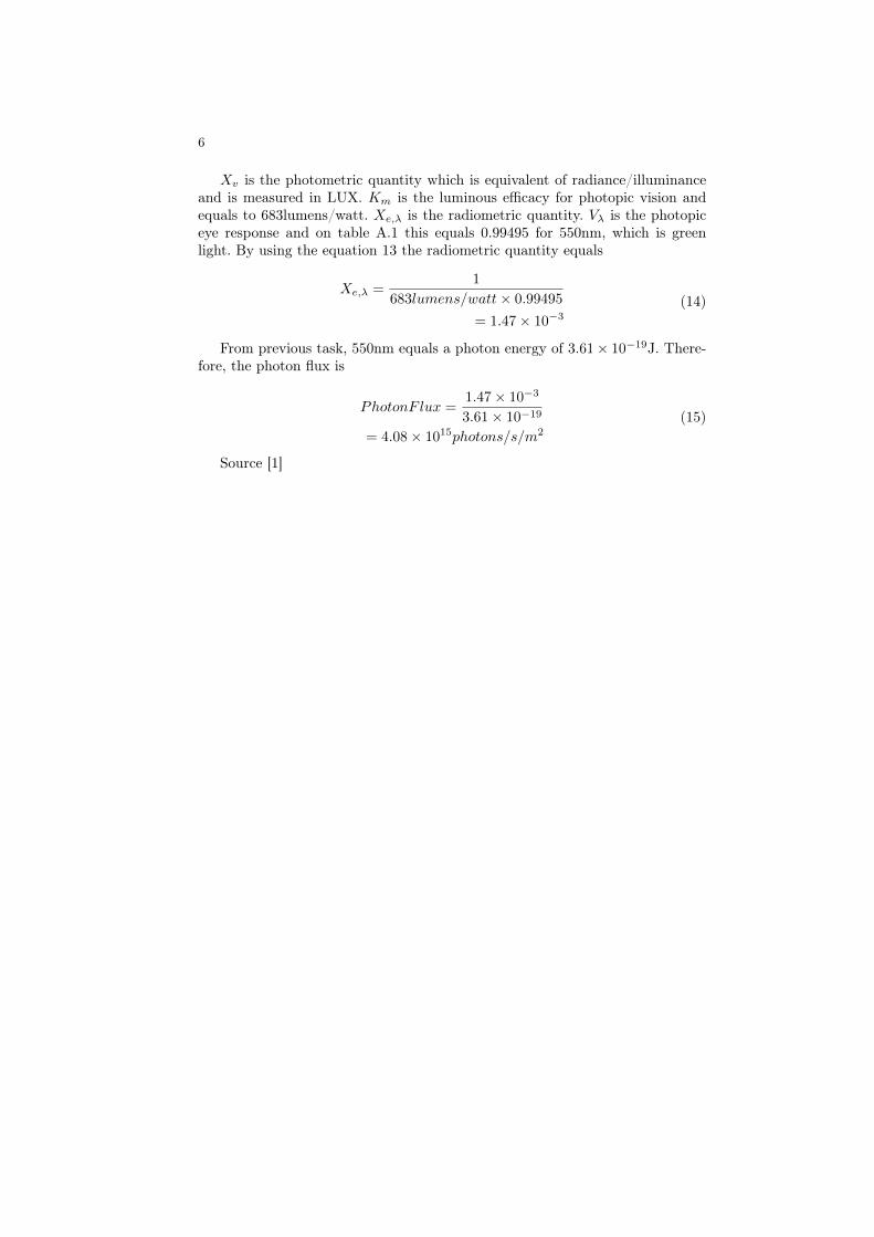
The Appendix A: Number of incident photons per LUX with a standard lightsource describes the parameters and equations used to measure photon flux[photons/m2/sec]. By using the equation A.1
Xv = Km
∫ λ2
λ1
Xe,λ × V (λ)δλ (13)
6
Xv is the photometric quantity which is equivalent of radiance/illuminanceand is measured in LUX. Km is the luminous efficacy for photopic vision andequals to 683lumens/watt. Xe,λ is the radiometric quantity. Vλ is the photopiceye response and on table A.1 this equals 0.99495 for 550nm, which is greenlight. By using the equation 13 the radiometric quantity equals
Xe,λ =1
683lumens/watt× 0.99495
= 1.47× 10⁻³(14)
From previous task, 550nm equals a photon energy of 3.61× 10⁻¹⁹J. There-fore, the photon flux is
PhotonF lux =1.47× 10⁻³
3.61× 10−19
= 4.08× 10¹⁵photons/s/m2
(15)
Source [1]
INF5442 7
2 Exercise 2
2.1 Define cut-off wavelength, and what is the value for silicon
The photons hitting the image sensor’s pixels must have a certain amount ofenergy to free electrons from their valence band into the conduction band region.Given that the energy of a photon is dependent of the wavelength of the photonsand the maximum wavelength that is capable of exciting the electron is called thecut-off wavelength, λcutoff . Generally it means the photodiode can sense up tothis wavelength, any wavelength larger than λcuttoff will not generate electronsin the pixel and instead pass right through. In silicon λcuttoff is approximately1.1µm.
2.2 50% of red, green, and blue light in silicon is absorbed atwhich depth
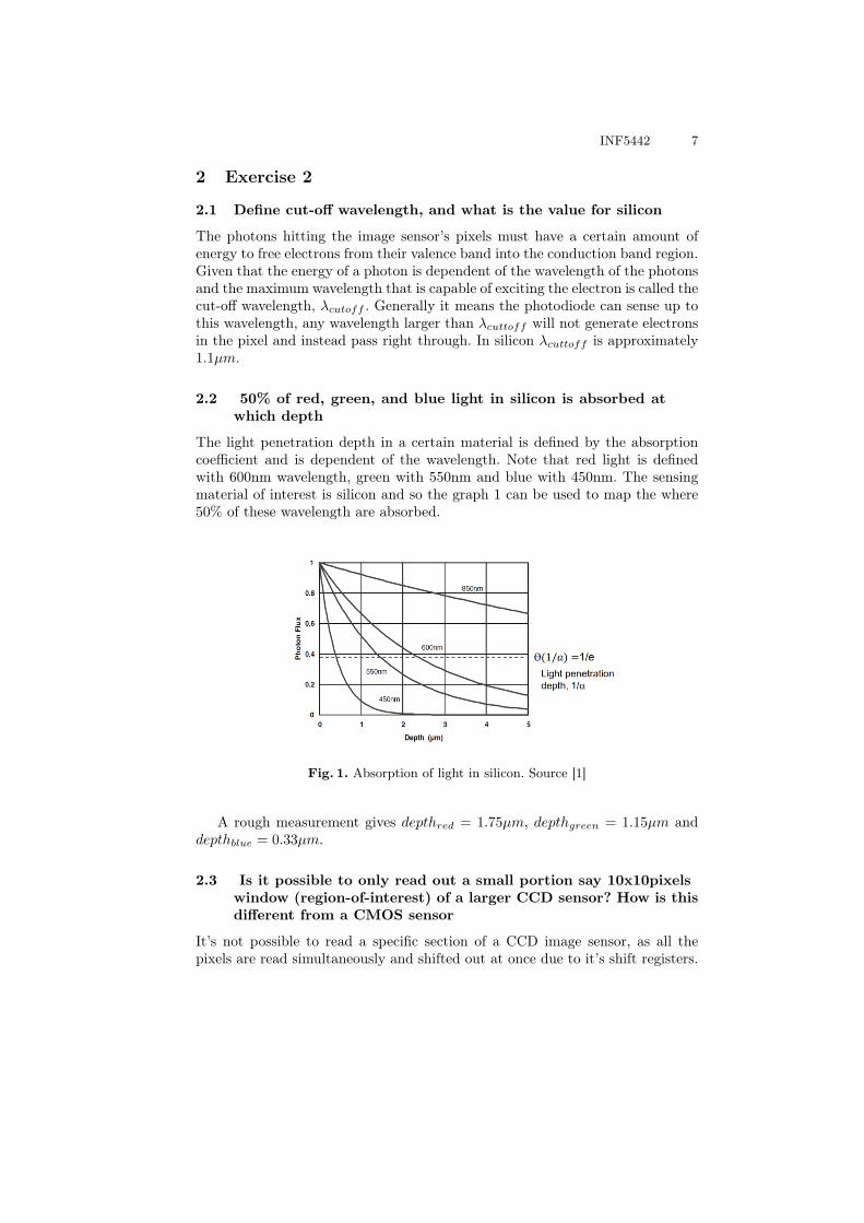
The light penetration depth in a certain material is defined by the absorptioncoefficient and is dependent of the wavelength. Note that red light is definedwith 600nm wavelength, green with 550nm and blue with 450nm. The sensingmaterial of interest is silicon and so the graph 1 can be used to map the where50% of these wavelength are absorbed.
Fig. 1. Absorption of light in silicon. Source [1]
A rough measurement gives depthred = 1.75µm, depthgreen = 1.15µm anddepthblue = 0.33µm.
2.3 Is it possible to only read out a small portion say 10x10pixelswindow (region-of-interest) of a larger CCD sensor? How is thisdifferent from a CMOS sensor
It’s not possible to read a specific section of a CCD image sensor, as all thepixels are read simultaneously and shifted out at once due to it’s shift registers.

8
CMOS image sensors, on the other hand, can read a small section of pixels. Theyuse row and column decoders which makes it possible to select a specific rowand then the column of interest, so it’s still restricted and can’t read the pixelsoutside of the range of rows or column being selected.
2.4 Why are CCD sensors limited to analogue output, only? Whynot integrate A/D converters and digital signal processingcircuits
CCD fabrication process differs from the general CMOS based process and istherefore inefficient in terms of cost and performance. The transistors producesfor digital circuit usage are poor and is more beneficial and efficient to sepa-rate these. As CCD image sensors are large in size due to their shift registers,including digital circuit parts will only increase the total die size of the chip.
2.5 Explain the difference between global shutter and rollingshutter readout
In a global shutter the start and end of the integration time is the same andhappens simultaneously for the entire pixel array. This means the whole image iscaptured at the exact same time with no delay. In rolling shutter the integrationtime is the same for all pixels, but starts and ends at a different time, often witha small delay between each row and hence the given name rolling shutter. Theintegration time begins with a single row and and the next one begins when it’sdone and the read out process begins. This means the scene is being capturedrow by row.
2.6 What are the pros and cons of CCDs versus CMOS imagesensors
CCD CMOSPros Cons Pros Cons
Has global shutter andprevents distortion
Low resolutionandlarge die size
Low powerconsumption
If running on rolling shutter,it suffers from distortionand artefacts
High signal to noise ratio The manufacturingprocess is expensive
Has integrateddigital circuits Less sensitive to light
High power consumptiondue to shift registers
Cheaperto produce
INF5442 9
2.7 Explain the artefacts that can occur when rolling shuttersensors capture fast moving objects
As a rolling shutter captures the scene rows by row, there is a certain delaybetween each row and this delay can cause
– Skew: Diagonal bend as the camera or object moves, capturing parts of theobject at different times.
– Smear: This artefact appears when something is rotating quickly (propeller).The smear of each blade is caused by the propeller rotating at the same ornear the same speed that the frame is read by the camera.
Other artefacts a rolling shutter suffers from are:
– Partial Exposure: If a flash goes on only partial of the exposure time, theflash may only be present at certain rows of the pixelarray in a given frame.
– Wobble: This phenomenon occurs when the camera isn’t stable, but vibrat-ing. The resulting image will appears to wobble and is blurry.
2.8 Why do most CMOS image sensors use rolling shutter insteadof global shutter
A rolling shutter sensor will have less noise and a wider dynamic range than aglobal shutter. To apply global shutter, the image sensor will need an additionalspace for saving the actual signal accumulated by light, such as an internalcapacitor separated from the photodiode or external memory. Both schemesrequires additional space and increases the chip size, also an internal capacitorwill reduce the fill factor.
2.9 Let a 10x10um ideal photon detector be illuminated by 10kphotons. What is its signal/noise ratio
Since no read noise value is presented in the task, it is assumed photon shotnoise is dominant. Therefore, the equation 3.47[1] can be used
SNR = 20log√Nsig
= 20log√10k
= 40dB
(16)
10
3 Exercise 3
3.1 Define conversion gain
Conversion gain is the measure of voltage change caused by a single electron atthe charge detection node. It is expressed as:
C.G =q
CFDµV/e− (17)
Where q is the charge and CFD is the charge-to-voltage conversion capaci-tance (floating diffusion capacitance)
3.2 A 2.2um 4T pixel has maximum output voltage swing of 1.1V,and FWC is 14ke-. What is the conversion gain? You canassume source follower gain of 0.8
The maximum voltage output swing is the value after the amplification
VC.G =1.1V
0.8= 1.375V (18)
To find the conversion gain, the equation for voltage swing at the FD can beused
∆VFD = C.G× Selectrons (19)
by rearranging the formula, the C.G can be found
C.G =∆VFDSelectron
=1.375V
14000e−= 98µV/e−
(20)
3.3 If temporal noise floor is 2.3e- rms, what is the dynamic rangeof this pixel
No parameters are given, therefore parameters from the previous task are used.
DR = 20logFWC
nnoise
=14000e−2.3e−= 75dB
(21)

INF5442 11
3.4 Why does Q.E for short wavelengths eventually drop to zero
The photons entering the pixel and hitting the photodiode, which generateselectron-hole pairs by the photon energy. The depth at which these pairs aregenerated depends on the wavelength of the photon. When the wavelength istoo short, the photons will only manage to reach the surface of the pixel. In thiscase the energy is either absorbed in this area or reflected and as a result, photonsof short wavelength do not reach the depletion area. Therefore, no charge aregenerated due to short wavelength and the quantum efficiency drops to zero.
See figure 3.5
3.5 Why does Q.E for long wavelengths eventually drop to zero
If the photon energy is not sufficient to generate electron-hole pair, the photonwill only pass through the semiconductor. Photon energy is inversely proportionto its wavelength. At higher wavelength, the photon energy is not sufficientenough to excite the electrons from it’s band. Hence, the quantum efficiencydrops to zero.
See figure 3.5
Fig. 2. Q.E graph
3.6 Why does Bayer RGB pattern have twice as many green pixelsas red and blue
Human eye perception is more sensitive to the colour green compared to red andblue. By taking advantage of this property, the Bayer RGB pattern adds moregreen pixels to the colour filter to mimic the human visual system. The resultingimage will appear less noisy and has finer details compared to a filter with equalquantities of RGB.
12
3.7 Can you list three types of fixed pattern noise sources
– Dark current variation – This is due to the charge integrated when pixelis not exposed to light. The reasons for this are the leakage current in thetransistors and the electrons generated due to temperature.
– Photo-response non-uniformity – The voltage amplification at pixel ampli-fiers is not uniform because of process variation. Hence, the signal generationat pixels are non-uniform.
– Vertical FPN – Noise created due to process difference in each transistor andcreating an offset for each column during readout.
3.8 List three types of temporal noise sources
– Thermal noise – This noise occurs due to the movement of electrons withinresistance due to the temperature and is always present above 0 K.
– Photon shot noise – This is due to the inherent natural variation of theincident photon.
– Flicker (1/f) noise – This noise is due to the surface states that occur dueto abrupt discontinuity in semiconductor lattice. These states are caused bydangling bonds at the surface. They combine with the charge and contributeonly in low frequency.
– Reset (kTC) noise – This is caused by the MOS switch used to reset thefloating diffusion capacitance. This comes from the thermal noise of the MOSswitch resistance and is sampled and held by the capacitor, which adds tothe signal.
3.9 Explain how FPN can be removed in pictures
FPN can be removed from pictures with Black Level Subtraction technique.A picture is first captured with the shutter closed and thus a dark image isobtained. This dark image will contain the offsets of the pixels at the specificexposure time and temperature, varying these factors can change the FPN. Apicture of the desired scene is then captured with the same exposure time andunder same temperature and by subtracting the dark image from it will removeall the offsets, producing an image free of FPN.
3.10 Explain how temporal noise can be removed in pictures
Temporal noise varies in time and is dependent of the environment. A simplemethod to reduce it’s effect can be accumulating more signal by increasing theexposure time and hence increasing SNR. Dark current can be reduced by reduc-ing the size of the pixel and using pinned photodiode. Thermal noise and flickernoise can be reduced by optimising the amplifier design by adjusting the (W/L)ratio of the amplifier. Correlated Double Sampling technique helps reduce bothkTC noise and flicker noise. This technique samples both the reset value andthe signal and taking the difference between the two. This will remove the noise

INF5442 13
present in the pixel and providing the actual voltage drop regardless of the resetvalue. Thus the reset value needs to be the same as the one the signal is droppingfrom.
3.11 Calculate the standard deviation of the number ofphoto-electrons accumulated in a pixel whose average (mean)value is 1000e-. Assume only photon shot noise. What is thesignal/noise ratio of the pixel
Photoelectricity is random by nature and follows the Poisson’s probability distri-bution. Following the Poissonian process, the variance value is equal to the meanvalue, µ, and the standard deviation, σ, is the the square root of the variance.Therefore, the standard deviation is
σ =√µ
=√1000
= 31.623
(22)
As the task mentioned to only assume photon shot noise means the numberof electron generated is equal to the average value, 1000e-. Using the formula forSNR
SNR = 20logµ√µ
= 30dB (23)
3.12 If “noise” in a sensor is generally considered to be random(non-deterministic) deviation from its mean value (averagevalue), explain why a “fixed” (deterministic) pattern in imagesensors is considered to be “noise”
Fixed pattern noise in image sensor is only fixed in spatial domain and not intime domain. It means that the intensity of the pattern obtained does differs ifthe environment changes, such as the temperature, exposure time or illuminationsource. In this case the noise is not deterministic and hence, fixed pattern noiseis considered noise. Another reason is that the fixed pattern noise varies froma sensor to another due to process variation and no sensors has the exact samefixed pattern noise despite the images are taking with the exact same condition.Last, but not least, noise deteriorates an image and it’s quality and is thereforeconsidered as a noise component.
14
4 Exercise 4
4.1 What is meant by ‘black level’ in a digital picture
Black level is the darkest value in an image with no illumination source present.Due to noise, the output of the pixels are rarely zero and produces a non-zerovalue from the ADC and is known as the black level. This level can be measuredby either capturing an image in total darkness or using the optical black pixels.
(I’m not sure if the answer is correct. According to the slide on lecture 4,page 7, ADC output values non-zero even if pixel output signal is zero(??) andis therefore necessary to add an offset in the ADC input to achieve a certainlevel and subtracts afterwards. As I understood it, this level is the Black LevelCompensation.)
4.2 List possible reasons why a digital camera has a non-zero blacklevel
The main cause for a non-zero black level in digital cameras are due to darkcurrent, offset voltage from the PGA and read noise from the ADC. Dark currentarises due to thermal agitation of electrons in the analogue circuits and currentleakage (see previous exercises).
4.3 Explain why black level must be subtracted before beingprocessed in the signal processing data path inside a camera.Give an example what can happen
Black level is an undesired offset which affects the the resulting image by pro-ducing false colour and illumination representation of the scenery. During digitalsignal processing, such as colour interpolation and auto white balance, the ad-ditional offset value will cause a poor approximation of the actual colour in thescene. A non-zero black level limits the usage of the linear region, affecting thedynamic range, which affects the quality of the image and deceasing the dynamicrange. Instead of starting from 0, the linear region begins from the offset valueand causes the bright values to saturate earlier, hence losing information in thebright region.
4.4 What is the role of the demosaicing (aka colour interpolation)algorithm
Image sensors have a colour filter array above it’s sensor, typically in a Bayer’spattern. This causes the pixels to capture only a single colour, either red, blue orgreen, while the information of the other colours are absent. In order to recon-struct the image with the correct or decent representation of the scenery, thesepixels needs the other two values to recreate the correct colour. This is doneby using colour interpolation algorithms. The process finds the actual colourby measuring the neighbouring values and calculates an approximation or av-erage value by either using "Nearest Neighbour Interpolation", "Bilinear" or"(Bi)Cubis Interpolation".
INF5442 15
4.5 What artifact(s) can demosaicing introduce in the image?What, if anything, can be done to mitigate such issue(s)
The artefacts demosaicing introduces occur when the spatial frequency of thescenery is higher than the resolution of the image sensor. The demosaicing pro-cess will struggle to find the proper colour representation of that area. There aretwo main artefacts: Misguidance Colour Artefacts and Interpolation Artefacts[3].
Misguidance colour artefacts are “False colour” and “Zipper effect”. Falsecolour effect occurs when the process struggles to find the proper colour andassigns a false colour around the area, typical near the edges or fine details.Zipper effect produces an abrupt change in intensity or colour, mainly near theedges, due to difficulty of estimation.
Interpolation artefacts are related to the limitation of the interpolation algo-rithm itself and is less noticeable.
Or...The artefact demosaicing introduces is aliasing. Aliasing occurs due to spatial
high frequency which the sensor is incapable of resolving and colour interpolationenhances the effect. This is due to the details found in the scenery are too smallcausing a single pixel to capture it or the change of colour, creating discolourationor interference in the resulting image. This can be seen as incorrect colour,intensity or pattern which doesn’t exist in the scenery itself.
To mitigate demosaicing artefacts, an optical low-pass filter can be includedto reduce the effect or increase the resolution of the image sensor. The use ofhigher order or more complex algorithm can also reduce the effect, but affectsthe speed.
4.6 Explain the principle role of the colour correction matrix in adigital camera
Colour Correction Matrix (CCM) is created to compensate for colour cross-talkbetween the pixels. Along with colour filter, each pixel registers only a singlespectral, but the filter is not ideal due to process variation. This causes chargeaccumulation, the photodiode absorbs photons despite not being the desiredwavelength. CCM coefficients defines the level of colour cross-talk between pixelsand adjust the R, G, B values to compensate.
4.7 If a CCM equals a unity matrix with only 1s in the diagonaland 0s all other coefficients, what does it say about the sensorspectral response
If CCM equals a unity matrix with only 1s in the diagonal and 0s coefficients,based on the information from previous task, means that there is no colourcrosstalk and the colour filter is ideal.

16
4.8 Explain why large CCM coefficients outside the diagonal resultin noisy images
A large CCM coefficients outside the main diagonal equals to a large colourcrosstalk. This level of colour interference, assuming is overwhelming comparedto the values in the diagonal, will make it hard to assume the real colour of theactual pixel value. This results in a low SNR, hence making the resulting imagenoisy.
4.9 Can the CCM matrix be adjusted to compensate for changesin the scene illumination spectrum? If yes, explain how
CCM are pre-calculated in the software before a camera is sold and the valuesare calculated based on the existing colour crosstalk. Therefore, the coefficientscan’t be adjusted to compensate for the scene illumination. Although, a camerausually has more than a single CCM, typically 3, and one can chose betweenthese.
INF5442 17
5 Exercise 5
5.1 Can you think of reasons why most tone mapping curves usehigh gain in dark region and low gain in bright region of thepicture
Tone mapping are required to map images from higher resolution devices tothose with lower resolution, typically 12bits to 8bits. As human is more sensitiveto variances within the dark region compared to the bright region, by using highgain at the dark region and low gain in bright region the tone mapping curvetakes advantage of the way human perceives light. Another reason to use lowgain at the brighter region is to prevent the values from saturating, hence losingthe information accumulated by natural illumination. If linear mapping is used,the resulting image will have low contrast and less pleasant to see.
5.2 Assume a video camera is capturing a scene where the sun isabout to disappear behind a cloud; hence more brightness isneeded in the picture. What should change first, integrationtime or gain, and explain why made that choice
The integration time should always be the first factor to increase. This allowsthe image sensor to accumulate more charges and resulting in an image with abetter quality and higher SNR. By increasing gain, the noise will be amplifiedas well, which reduces SNR.
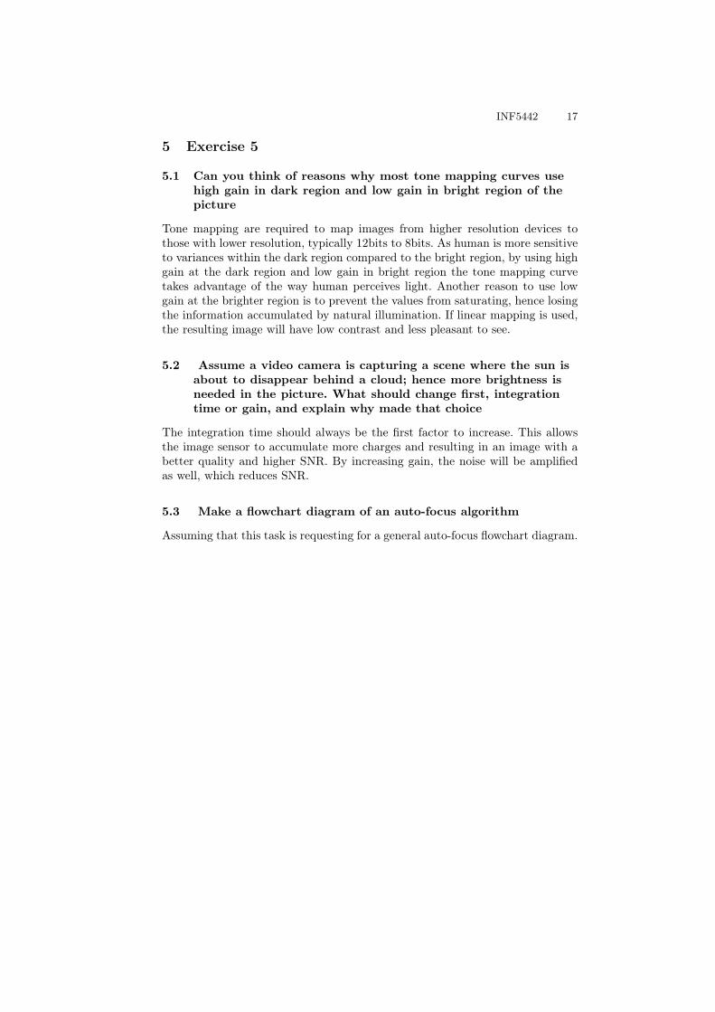
5.3 Make a flowchart diagram of an auto-focus algorithm
Assuming that this task is requesting for a general auto-focus flowchart diagram.
18
Fig. 3. A simple flow chart diagram of adjusting the lens for auto-focus
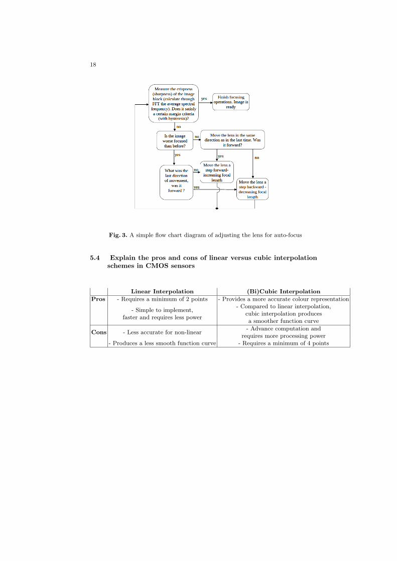
5.4 Explain the pros and cons of linear versus cubic interpolationschemes in CMOS sensors
Linear Interpolation (Bi)Cubic InterpolationPros - Requires a minimum of 2 points - Provides a more accurate colour representation
- Simple to implement,faster and requires less power
- Compared to linear interpolation,cubic interpolation producesa smoother function curve
Cons - Less accurate for non-linear - Advance computation andrequires more processing power
- Produces a less smooth function curve - Requires a minimum of 4 points
INF5442 19
6 Exercise 6
6.1 List the three data reduction concepts used in JPEGcompression
– Sub-sampling chrome information– Discrete Cosine Transformation (DCT)– Quantization– Run Length Coding(RLC)– Entropy Encoding
6.2 Why does JPEG use YCbCr instead of RGB data
Human visual system is more sensitive to variance in luminance compared tochromiance. To adapt this property, YCbCr is a preferable scheme. It separatesY, luminance, from the chroma, Cb and Cr, providing the opportunity to workwith these individually. Further, the chroma information is then reduced byremoving partial of these components without actually reducing the quality ofthe image.
6.3 Why does JPEG group image data into blocks of 8x8 pixels
Transformation from spatial to frequency domain is performed in JPEG forenergy compaction i.e. limited number of transformed coefficients carry most ofthe signal energy. This requirement is met when the pixels in the average blockare correlated in spatial domain. An 8x8 block has a high correlation betweenpixels for energy compaction in the transformed matrix. It’s proven throughstudies to be the optimal size for computation purpose, requiring less memoryspace and inexpensive hardware implementation.
A smaller block size can struggle to capture the important pixel-to-pixelcorrelation. A larger block sizes can be too big, containing uncorrelated pixelsand requires higher computation complexity.
6.4 What is the purpose of DCT in JPEG
Dicrete Cosine Transformation (DCT) transforms the micro blocks from the spa-tial domain to the frequency domain. This is done to find the high frequencycomponents and to further discard these. The resulting block consists of a singleDC coefficient, the largest value, at the upper-left corner and 63 AC coefficientsfor each frequency. This process concentrates the signals in one corner and pro-vides a more effective compression later.
20
6.5 What is the purpose of quantization in JPEG
Quantization process takes the 8x8 micro blocks, produced by the DCT, anddivides them by using a quatization matrix, a lowpass filter. The elements inthe matrix controls the compression ratio, where a larger values increases thecompression rate and vice versa. The values are then rounded to nearest integerand higher frequency components are rounded to zero.
The main purpose is to achieve smaller positive or negative values, whichrequires fewer bits to represent, and removing the high frequency componentsby setting these to 0. Human visual system can’t distinguish the exact strengthof a high frequency brightness variation and therefore this operation does notaffect the resulting image.
6.6 What step(s) makes JPEG compression lossy
Sub-sampling is lossy since partial of the chroma information is discarded. Thequantization is considered to be the most lossy operation in the whole processbecause values are rounded and it’s irreversible.
6.7 What is the basic concept used in entropy encoding schemessuch as Huffman encoding
Entropy encoding, a lossless data compression, involves arranging block in azigzag pattern by employing run length coding(RLC) algorithm and further com-pressing it by allocating bits to the resulting code. The RLC algorithm groupsthe same frequency and because the data inside the block has high correlationthe frequency reoccurs throughout. The concept of entropy encoding is to sortthe frequency groups in terms on occurrence and allocate few bits to those withfrequent occurrence and longer bits to the rare.
INF5442 21
7 Exercise 7
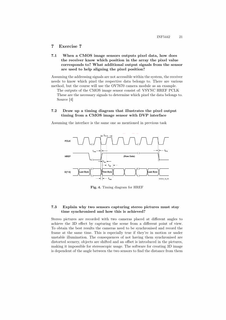
7.1 When a CMOS image sensors outputs pixel data, how doesthe receiver know which position in the array the pixel valuecorresponds to? What additional output signals from the sensorare used to help aligning the pixel position?
Assuming the addressing signals are not accessible within the system, the receiverneeds to know which pixel the respective data belongs to. There are variousmethod, but the course will use the OV7670 camera module as an example.
The outputs of the CMOS image sensor consist of: VSYNC HREF PCLKThese are the necessary signals to determine which pixel the data belongs to.Source [4]
7.2 Draw up a timing diagram that illustrates the pixel outputtiming from a CMOS image sensor with DVP interface
Assuming the interface is the same one as mentioned in previous task
Fig. 4. Timing diagram for HREF
7.3 Explain why two sensors capturing stereo pictures must staytime synchronised and how this is achieved?
Stereo pictures are recorded with two cameras placed at different angles toachieve the 3D effect by capturing the scene from a different point of view.To obtain the best results the cameras need to be synchronised and record theframe at the same time. This is especially true if they’re in motion or underunstable illumination. The consequences of not having them synchronised aredistorted scenery, objects are shifted and an offset is introduced in the pictures,making it impossible for stereoscopic usage. The software for creating 3D imageis dependent of the angle between the two sensors to find the distance from them

22
Fig. 5. Readout timing diagram for a "VGA" (640 x 480)
to the actual scene. The distance is then used to pinpoint a specific position inthe scene found on both sensors and ensure that the given points are the exactsame point in the real scene.
The two cameras can be synchronised by using a common clock source and/orshared trigger for capture. It should be noted that they should share exposuretime and settings to ensure maximum cohesion between the resulting imagesfrom the sensors.
7.4 What is a pull-up resistor? What purpose does such a circuitserve?
A pull-up resistor is a resistor connected between pins, such as MCU or IC, andVDD. The common impedance for a pull-up resistor is 10K or 100KOhm. Thisis used to set the floating line to a known state by "pulling" it up to VDD. TheMCU or IC can tell whether the line is active or inactive by seeing the state theline is in. Another purpose of this component is that it combats induced noisecreated by magnetic-fields.
7.5 A sensor outputs uses 12b DVP output with 100MHz pixelclock. Load on output pins is 20pF. VDDIO=1.8V. Calculateworst case current spike during transition and explain howthis can result in image noise. Calculate the average currentassuming 50% toggling rate. Why is high power a concern? Canyou suggest a method to reduce this power?
Considering the "worst case" is when all signals toggles at the same time andfrom task 1, the output signals for determining the pixel’s position needs to betaken into consideration. That would make a total of 15 signals: 12b DVP, clock,HREF and VSYNC.
INF5442 23
IV DDIO =Cload × VV DDIO
1fclk×4
×NDV Plines
=20× 10−12 × 1.8V
1100×106×4
× 15
= 216mA.
(24)
The average current, one needs to find the total power consumption anddivide it by the voltage. The task mentioned 50% toggling rate, so all signalsruns at half of the clock frequency. Although, the clock frequency remains thesame.
PIO = Cload × V 2V DDIO × fclk ×NDV P
= (20× 10−12 × 1.8V 2 × 50× 106 × 14) + (20× 10−12 × 1.8V 2 × 100× 106 × 1)
= 51.84mW(25)
The average current is then
Iavg =0.05184W
1.8V= 28.8mA (26)
High power consumption is of concern due to it contribution in increasingthe temperature of the chip and can cause damages to partial of the circuits.Large current spikes can induce supply and GND noise and cause variation atGND. The unstable GND will affect the other parts of the circuit. The sameoccurs for VDD as well and the power supply voltage can drop.
7.6 Why is the analogue supply voltage higher than the digitalsupply in most CMOS image sensors?
A higher voltage supply will provide analogue circuits a wider linear range towork with and improves it’s performance. It increases SNR, output swing andgain. Digital circuits do not require the same amount due to it only needs suf-ficient voltage level to differentiate 2 states; "0" and "1". A lower voltage sup-ply for digital circuits reduces power consumption and provides faster transi-tions/switch.
7.7 Why is it important to keep the voltage supplies as low-noiseas possible in CMOS image sensors?
In analogue circuits, a stable power supply is necessary to maintain its perfor-mance. In image sensor, the supply is connected directly to the photodiodesand the pixels outputs. A noisy power supply will affect these part directly interms of reset level and incorrect output values. Another important aspect isthe ADC. ADC uses the power supply as it’s main supply and reference signal.Therefore, if the supply is noisy it’ll create an undesired offset which will causemisinterpretation of values from the pixel array.
24
7.8 Why is external I/O supply voltage (DOVDD or VDDIO)typically separated from the internal digital supply voltage(DVDD)? Can the two values be different? If so, how is thishandled inside the chip?
External I/O voltage supply has a higher voltage, 3.3V to 5V, compared to theinternal digital supply voltage, which has 1.2V to 1.8V. As mentioned in previoustask, digital voltage supplies does not need to be any higher since the value onlyneeds to be high enough to differentiate "0" and what is known as "1". I/O padrequires a higher level due to it needs to drive the output capacitance and ESDcircuits. Another advantage of having separate supply is to reduce noise. I/Opads are often exposed to large currents and voltages, affecting it’s own suppliesand increases the temperature.
To achieve this a DC-DC converter, level shifter and a simple voltage dividercan be used.
7.9 Explain how CMOS I/O pins are ESD protected
A simple ESD circuit consists of two reverse biased diodes. Depending on thepolarity of the voltage, either too high or low, the upper diode will conduct orthe lower diode will conduct respectively and divert the voltage away from theinput. In some cases, current limiting resistors are included to prevent the diodeform burning out.
7.10 What does “tri-state of I/O pins” mean? Why is this conceptused?
A tri-state I/O pins has 3 states: logic high, low and high impedance. When thepin does not receive any input it will be in high impedance state and logic highor low otherwise. This allows the pin to be connected to multiple transmissionline and reduces the quantity of I/O pads.
7.11 List at least three reasons why the CMOS image sensorindustry is starting to move away from parallel output andover to serial output
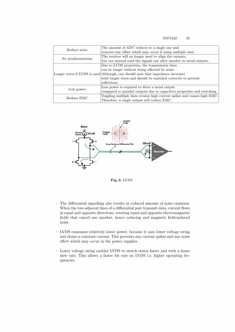
7.12 Draw a conceptual diagram of LVDS sender/receiver and listthe reasons why this has become such a popular industrystandard
– LVDS uses differential signals and is immune to common mode noise. Thismakes LVDS less sensitive to environmental noise and reduces the risk ofnoise related problems, such as crosstalk from neighbouring lines. As a result,LVDS can use a lower voltage swing compared with single-ended schemes.
INF5442 25
Reduce noise The amount of ADC reduces to a single one andremoves any offset which may occur if using multiple ones
No synchronisation The receiver will no longer need to align the outputs,but can instead read the signals one after another in serial outputs.
Longer wires if LVDS is used
Due to LVDS properties, the transmission linescan be longer without being affected by noise.Although, one should note that impedance increaseswith longer wires and should be matched correctly to preventreflections.
Low power Less power is required to drive a serial outputcompared to parallel outputs due to capacitive properties and switching.
Reduce EMC Toggling multiple lines creates high current spikes and causes high EMC.Therefore, a single output will reduce EMC.
Fig. 6. LVDS
– The differential signalling also results in reduced amount of noise emission.When the two adjacent lines of a differential pair transmit data, current flowsin equal and opposite directions, creating equal and opposite electromagneticfields that cancel one another, hence reducing and magnetic field-inducednoise.
– LVDS consumes relatively lower power, because it uses lower voltage swingand draws a constant current. This prevents any current spikes and any noiseeffect which may occur in the power supplies.
– Lower voltage swing enables LVDS to switch states faster and with a lesserslew rate. This allows a faster bit rate on LVDS i.e. higher operating fre-quencies.

26
7.13 A CMOS sensor has 4+1 (4x data+ 1x clk) LVDS outputlanes. Calculate the estimated power consumption
Using the parameters found in lecture notes for an LVDS interface lane of 3Gb/sdata transfer, each data lane would require 8.75mW and the clock rate needs tobe 2 times faster than the data.
Ptot = (4 ∗ 8.75mW ) + (1 ∗ 2 ∗ 8.75mW )
= 52.5mW(27)

Bibliography
[1] Junichi Nakamura. Image sensors and signal processing for digital still cam-eras. CRC press, 2016.
[2] Wien’s displacement law. https://en.wikipedia.org/wiki/Wien%27s_displacement_law. Accessed: 2017-02-12.
[3] Ruiwen Zhen and Robert L Stevenson. Image demosaicing. In Color Imageand Video Enhancement, pages 11–22. Springer, 2015.
[4] Jorge Aparicio. Hacking the OV7670 camera mod-ule. http://embeddedprogrammer.blogspot.no/2012/07/hacking-ov7670-camera-module-sccb-cheat.html, 2012.
![An integrated optical transient sensor - Circuits and …...of biologically-inspired image-processing circuits that perform such functions as motion-sensing [13], attentional selection](https://img.pdfslide.us/doc/110x75/5fb6327627bd894f23726ba4/an-integrated-optical-transient-sensor-circuits-and-of-biologically-inspired.jpg)