Embed Size (px)
Citation preview
© iNEMI 2013
iNEMI Lead-Free Rework Optimization
Project: Phase 3-Assembly and
Rework Evaluation
Project Co-Chairs:
Jasbir Bath (INEMI)
Craig Hamilton (Celestica)
Holly Rubin (Alcatel-Lucent)
1 © iNEMI 2013 1
Background
• Reliability tests in the previous iNEMI lead-free assembly and
rework project indicated a need to initiate a follow on iNEMI
Rework Optimization Project.
• Thermal fatigue life of certain components on the iNEMI
Payette board such as the CBGA937 was reduced after
rework.
• The overall project would evaluate and recommend best
practices, rework equipment requirements, impact of adjacent
component temperatures and procedures for best practice
lead-free rework processing.

2 © iNEMI 2013 2
Lead-Free Rework Optimization Project Phase 3
Phase 1 and 2 of the project have:
1. Determined rework repeatability on a range of rework equipment
2. Developed initial rework processes for mini-pot rework
3. Optimized BGA socket rework processes
4. Developed rework processes for uBGAs to prevent adjacent component reflow
Phase 3 project is to:
Assemble and Rework Boards with the developed rework processes and perform reliability testing to validate the rework processes developed

3 © iNEMI 2013 3
iNEMI Rework Optimization Project Participants
– Celestica, Sanmina-SCI, Plexus, Flextronics, Creation
– Cisco, Alcatel-Lucent
– Intel
– Senju, Nihon Superior

4 © iNEMI 2013 4
iNEMI Rework Optimization Project (Phase 3)
– Board redesign for DIMM daughter card: (Plexus)
– Board build for iNEMI Payette board and DIMM daughter card:
(Sanmina-SCI)
– SMT board and Wave assembly: (Creation)
– BGA socket rework: (Intel)
– uBGA rework: (Flextronics)
– DIMM and DIP rework (Celestica)
– ATC thermal cycling (Alcatel-Lucent)
– ATC thermal cycled board cross-sections (Plexus, Intel, Nihon
Superior, Alcatel-Lucent)
5 © iNEMI 2013
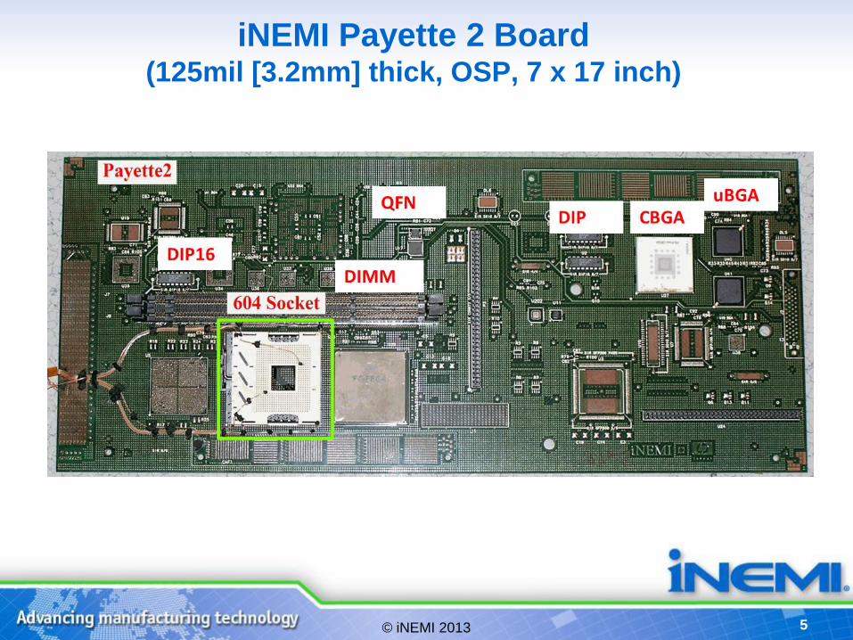
iNEMI Payette 2 Board (125mil [3.2mm] thick, OSP, 7 x 17 inch)
6 © iNEMI 2013
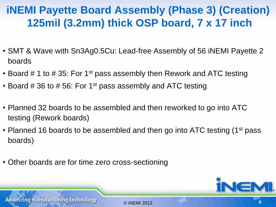
iNEMI Payette Board Assembly (Phase 3) (Creation)
125mil (3.2mm) thick OSP board, 7 x 17 inch
• SMT & Wave with Sn3Ag0.5Cu: Lead-free Assembly of 56 iNEMI Payette 2
boards
• Board # 1 to # 35: For 1st pass assembly then Rework and ATC testing
• Board # 36 to # 56: For 1st pass assembly and ATC testing
• Planned 32 boards to be assembled and then reworked to go into ATC
testing (Rework boards)
• Planned 16 boards to be assembled and then go into ATC testing (1st pass
boards)
• Other boards are for time zero cross-sectioning

7 © iNEMI 2013 7
SMT Reflow Profile (Topside)
Solder Joint peak temp.: 234 to 249°C.
Time over 217°C= 66 to 99 sec.
8 © iNEMI 2013
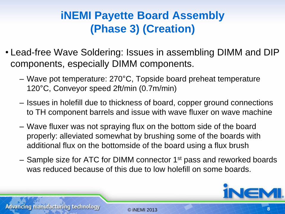
• Lead-free Wave Soldering: Issues in assembling DIMM and DIP
components, especially DIMM components.
– Wave pot temperature: 270°C, Topside board preheat temperature
120°C, Conveyor speed 2ft/min (0.7m/min)
– Issues in holefill due to thickness of board, copper ground connections
to TH component barrels and issue with wave fluxer on wave machine
– Wave fluxer was not spraying flux on the bottom side of the board
properly: alleviated somewhat by brushing some of the boards with
additional flux on the bottomside of the board using a flux brush
– Sample size for ATC for DIMM connector 1st pass and reworked boards
was reduced because of this due to low holefill on some boards.
iNEMI Payette Board Assembly
(Phase 3) (Creation)

9 © iNEMI 2013
iNEMI Payette Board Assembly (Phase 3) (Creation)
• Wave holefill issue on J7 DIMM278 I/O connector (Board #1, J7)
10 © iNEMI 2013
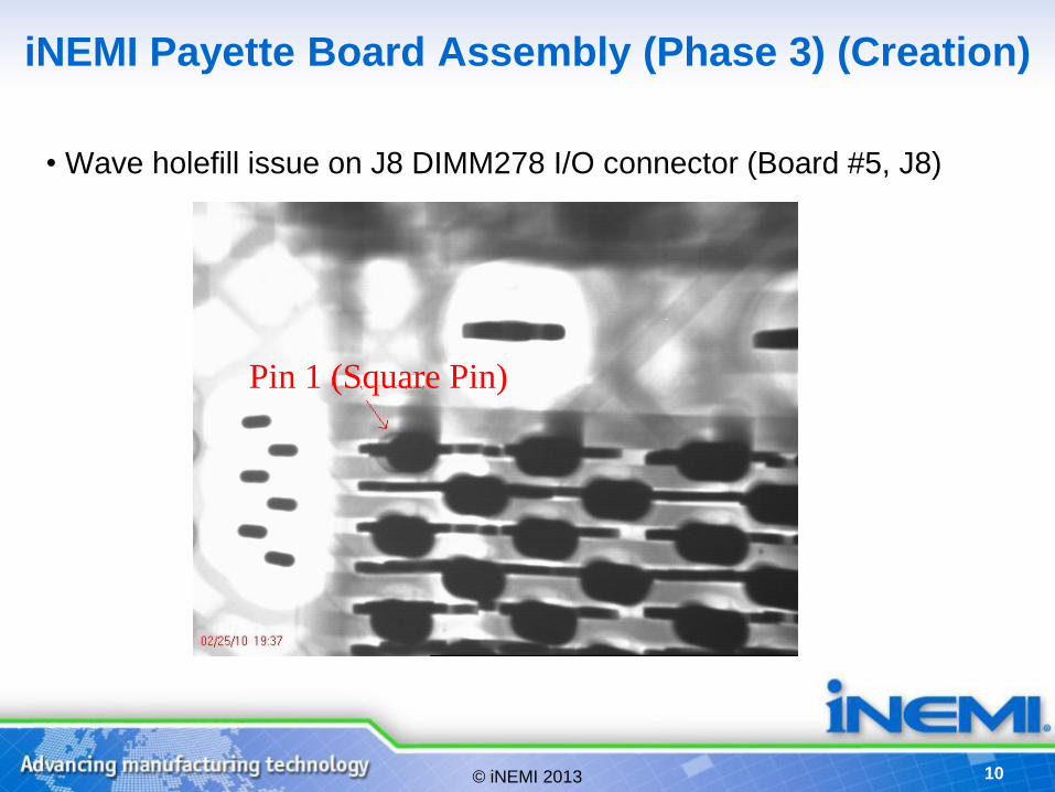
iNEMI Payette Board Assembly (Phase 3) (Creation)
• Wave holefill issue on J8 DIMM278 I/O connector (Board #5, J8)
Pin 1 (Square Pin)

11 © iNEMI 2013 11
– Adjacent Component Rework

12 © iNEMI 2013 12
Adjacent Component Group
iNEMI Payette board: Spacing between components is 0.5 inch (13mm)
Previous Findings
Based on previous J-STD-020 reflow parameters
– To maintain peak package temperature <250°C required increased bottom
heater temperatures
– Reworking the μBGAs with increased bottom heater temperatures caused
secondary reflow of the CBGA joints, and adversely impacted thermal fatigue life
13 © iNEMI 2013 13
Adjacent Component Group
Solutions Explored
– Heat shields
– Rework profile re-
optimization
Objectives
– Stay within J-STD-020D (260°C peak) parameters when reworking components
– Previous study work objective was to stay within 250°C peak temperature parameters when reworking components
– Ensure adjacent component joint temperatures remain below liquidus
14 © iNEMI 2013 14
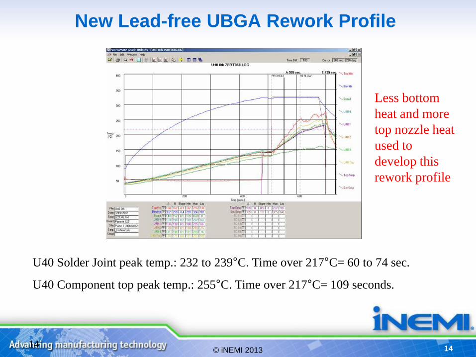
New Lead-free UBGA Rework Profile
U40 Solder Joint peak temp.: 232 to 239°C. Time over 217°C= 60 to 74 sec.
U40 Component top peak temp.: 255°C. Time over 217°C= 109 seconds.
Less bottom
heat and more
top nozzle heat
used to
develop this
rework profile
15 © iNEMI 2013
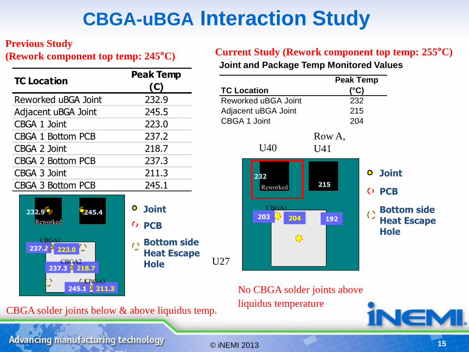
TC LocationPeak Temp
(C)
Reworked uBGA Joint 232.9
Adjacent uBGA Joint 245.5
CBGA 1 Joint 223.0
CBGA 1 Bottom PCB 237.2
CBGA 2 Joint 218.7
CBGA 2 Bottom PCB 237.3
CBGA 3 Joint 211.3
CBGA 3 Bottom PCB 245.1
Joint and Package Temp Monitored Values
CBGA solder joints below & above liquidus temp.
CBGA-uBGA Interaction Study Previous Study
(Rework component top temp: 245°C)
TC Location
Peak Temp
(°C)
Reworked uBGA Joint 232
Adjacent uBGA Joint 215
CBGA 1 Joint 204
215 Reworked
232.9 245.4
223.0 237.2
218.7 237.3
211.3 245.1
Joint
PCB
Bottom side Heat Escape Hole
CBGA1
CBGA2
CBGA3
Reworked
Current Study (Rework component top temp: 255°C)
No CBGA solder joints above
liquidus temperature
232
215
204 203
Joint
PCB
Bottom side Heat Escape Hole
CBGA1
Reworked
192
Row A,
U41 U40
U27
16 © iNEMI 2013 16
Conclusions
• A new lead-free rework profile was developed which kept the
adjacent CBGA solder joints below liquidus (217°C) whilst keeping
the reworked uBGA component within J-STD-020D limits.
– This was done by reducing bottom heat and increasing top nozzle heat
compared with previous study
• Found that heat shields (Al and Ceramic) helped to reduce the temperature
of the adjacent CBGA but not to a large extent (2°C to 4°C) so not used in
Phase 3
• Cross-sectional and electrical analysis of adjacent uBGA and CBGA:
• Electrical testing showed no change between as-assembled 1st pass
components (uBGA and CBGA) and those components adjacent to the
reworked uBGA
• Cross-sections of the adjacent uBGA at U41 next to reworked uBGA and
CBGA components showed well formed joints with no evidence of
secondary reflow
17 © iNEMI 2013 17
– BGA Socket Rework
18 © iNEMI 2013
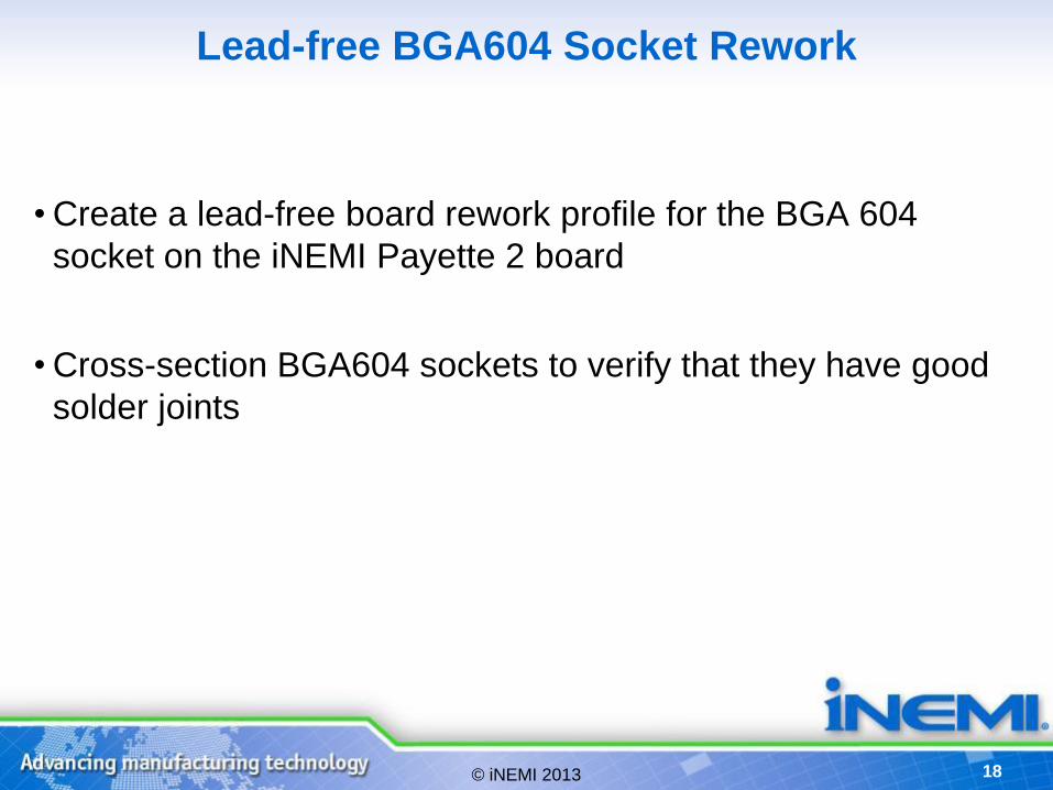
Lead-free BGA604 Socket Rework
• Create a lead-free board rework profile for the BGA 604
socket on the iNEMI Payette 2 board
• Cross-section BGA604 sockets to verify that they have good
solder joints
19 © iNEMI 2013
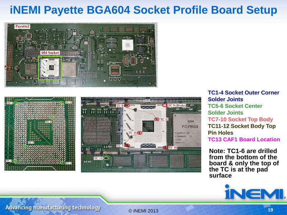
iNEMI Payette BGA604 Socket Profile Board Setup
TC1-4 Socket Outer Corner
Solder Joints
TC5-6 Socket Center
Solder Joints
TC7-10 Socket Top Body
TC11-12 Socket Body Top
Pin Holes
TC13 CAF1 Board Location
Note: TC1-6 are drilled from the bottom of the board & only the top of the TC is at the pad surface
20 © iNEMI 2013
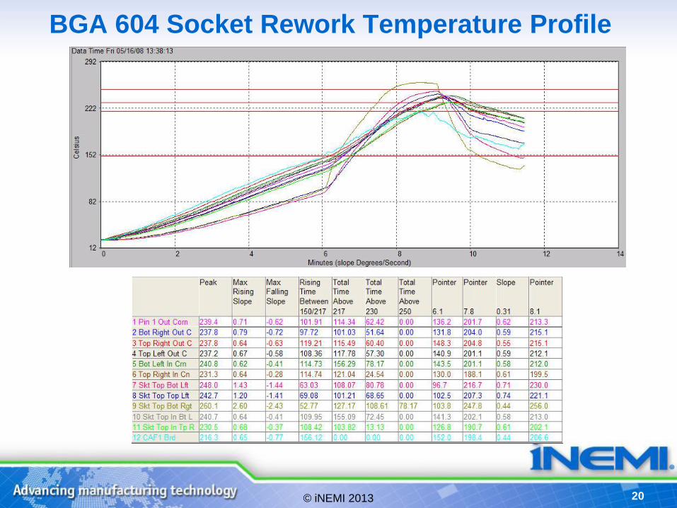
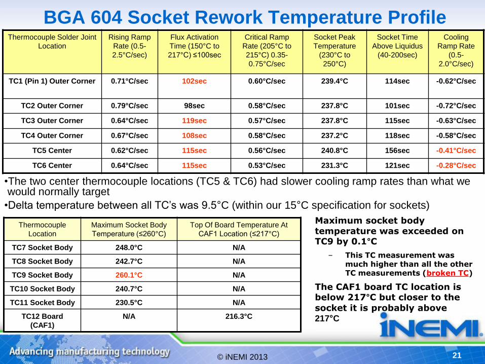
BGA 604 Socket Rework Temperature Profile
21 © iNEMI 2013
•Flux activation time is above our 100sec max target on all thermocouples except TC2 (highlighted in red)
• The maximum time exceeded was only 19sec & is due to the bottom heating system in the rework machine
•The two center thermocouple locations (TC5 & TC6) had slower cooling ramp rates than what we would normally target
•Delta temperature between all TC’s was 9.5°C (within our 15°C specification for sockets)
Thermocouple
Location
Maximum Socket Body
Temperature (≤260°C)
Top Of Board Temperature At
CAF1 Location (≤217°C)
TC7 Socket Body 248.0°C N/A
TC8 Socket Body 242.7°C N/A
TC9 Socket Body 260.1°C N/A
TC10 Socket Body 240.7°C N/A
TC11 Socket Body 230.5°C N/A
TC12 Board
(CAF1)
N/A 216.3°C
Thermocouple Solder Joint
Location
Rising Ramp
Rate (0.5-
2.5°C/sec)
Flux Activation
Time (150°C to
217°C) ≤100sec
Critical Ramp
Rate (205°C to
215°C) 0.35-
0.75°C/sec
Socket Peak
Temperature
(230°C to
250°C)
Socket Time
Above Liquidus
(40-200sec)
Cooling
Ramp Rate
(0.5-
2.0°C/sec)
TC1 (Pin 1) Outer Corner 0.71°C/sec 102sec 0.60°C/sec 239.4°C 114sec -0.62°C/sec
TC2 Outer Corner 0.79°C/sec 98sec 0.58°C/sec 237.8°C 101sec -0.72°C/sec
TC3 Outer Corner 0.64°C/sec 119sec 0.57°C/sec 237.8°C 115sec -0.63°C/sec
TC4 Outer Corner 0.67°C/sec 108sec 0.58°C/sec 237.2°C 118sec -0.58°C/sec
TC5 Center 0.62°C/sec 115sec 0.56°C/sec 240.8°C 156sec -0.41°C/sec
TC6 Center 0.64°C/sec 115sec 0.53°C/sec 231.3°C 121sec -0.28°C/sec
Maximum socket body temperature was exceeded on TC9 by 0.1°C
– This TC measurement was much higher than all the other TC measurements (broken TC)
The CAF1 board TC location is below 217°C but closer to the
socket it is probably above 217°C
BGA 604 Socket Rework Temperature Profile
22 © iNEMI 2013
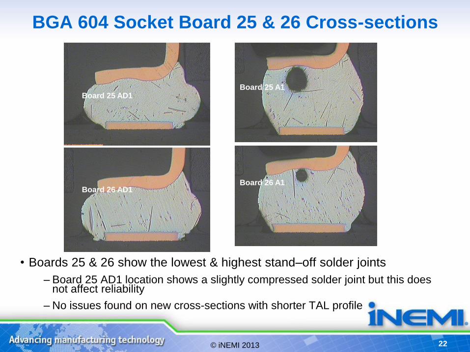
BGA 604 Socket Board 25 & 26 Cross-sections
• Boards 25 & 26 show the lowest & highest stand–off solder joints
– Board 25 AD1 location shows a slightly compressed solder joint but this does not affect reliability
– No issues found on new cross-sections with shorter TAL profile
Board 25 AD1 Board 25 A1
Board 26 AD1 Board 26 A1

23 © iNEMI 2013
• Board 22 cross-section shows that the socket warps down on A31 & AE2 corners
–A31 corner stand-off is approximately 2.5 mils lower
–AE2 corner stand-off is approximately 3.5 mils lower
• Boards 24, 25 & 26 cross-sections show only the AD1 corner to have a larger
collapse than all other measurements
–AD1 corner stand-off is approximately 3 to 5mils lower
• This is fairly common in socket rework from previous internal data that was obtained
Board # Cross-section Locations Stand-off Height Measurement Locations (mils)
22 A1-A31 & AE2-AE30 A1
16.68 A16
16.32 A31
14.34 AE2
12.15 AE16 15.59
AE30 15.73
24 A1-AD1 & A31-AD31 A1
17.12 M1
14.93 AD1 12.95
A31 15.73
M31 15.59
AD31 16.39
25 A1-AD1 & A31-AD31 A1
17.85 M1
14.20 AD1 12.66
A31 14.93
M31 14.85
AD31 16.68
26 A1-AD1 & A31-AD31 A1
15.73 M1
13.98 AD1 12.59
A31 14.71
M31 15.37
AD31 15.44
BGA 604 Socket Stand-off Results
24 © iNEMI 2013
BGA Socket Rework Summary
– The rework profile developed successfully
– The BGA socket stand-off measurements had up to a
5 mil delta across one side
• This is within the normal internal data range examined
– This was similar to the range observed on a different suppliers
BGA socket in previous studies
– IMC thickness measurements and elemental analysis
results were as expected
25 © iNEMI 2013 25
– Mini-pot Rework
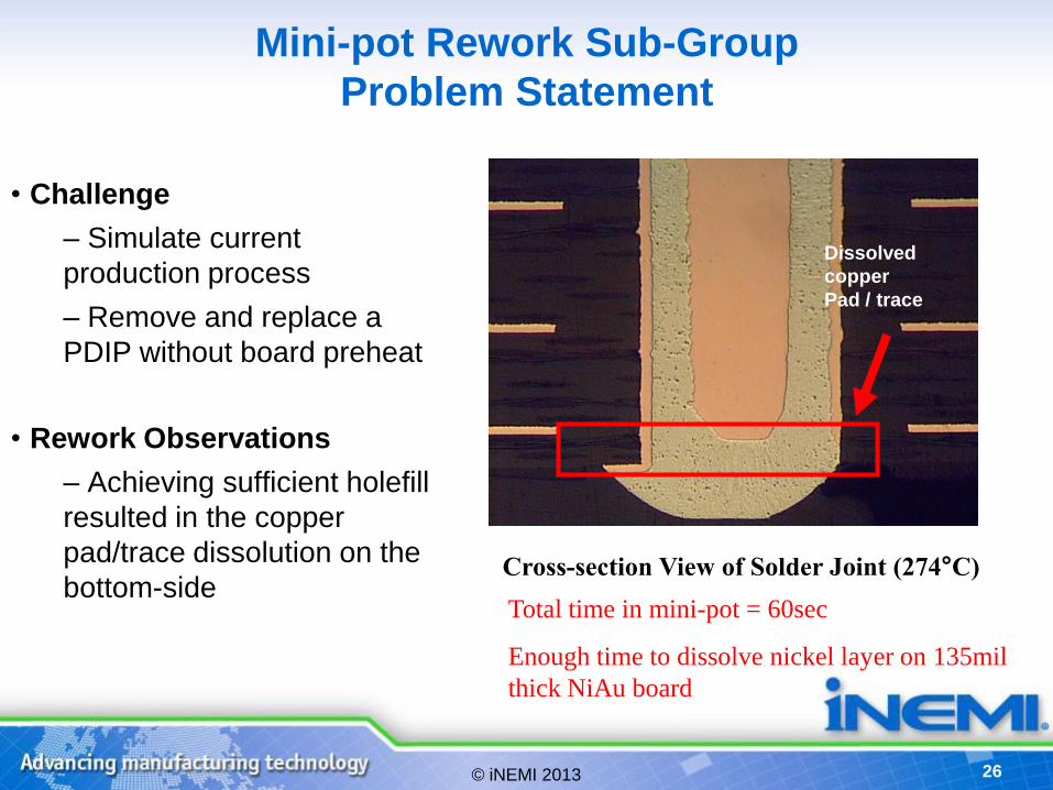
26 © iNEMI 2013
Cross-section View of Solder Joint (274°C)
Dissolved
copper
Pad / trace
Total time in mini-pot = 60sec
Enough time to dissolve nickel layer on 135mil
thick NiAu board
Mini-pot Rework Sub-Group
Problem Statement
• Challenge
– Simulate current
production process
– Remove and replace a
PDIP without board preheat
• Rework Observations
– Achieving sufficient holefill
resulted in the copper
pad/trace dissolution on the
bottom-side

27 © iNEMI 2013
Mini-pot Rework Status (Phase 1)
• Results on iNEMI Wave Test Board indicated that an alternative alloy from SnAgCu would be needed, in order to achieve up to a 2X PTH rework, without causing quality concerns
• Mixed Sn-Ag-Cu / Sn-Cu-Ni reworks included in Phase 2 and 3 builds
Sn-Ag-Cu Sn-Cu-Ni
1X Rework
2X Rework
Phase 1
• Variation in Cu plating thickness on incoming boards were observed
– First article inspection critical before Phase 2 and Phase 3 builds
– Needed to further understand specifications and process controls
used to monitor and control copper plating thickness for as-received
boards
Low Thermal Mass PCB (62mils)
Sn-Ag-Cu Sn-Cu-Ni
1X Rework
2X Rework X
High Thermal Mass PCB (145mils)
28 © iNEMI 2013
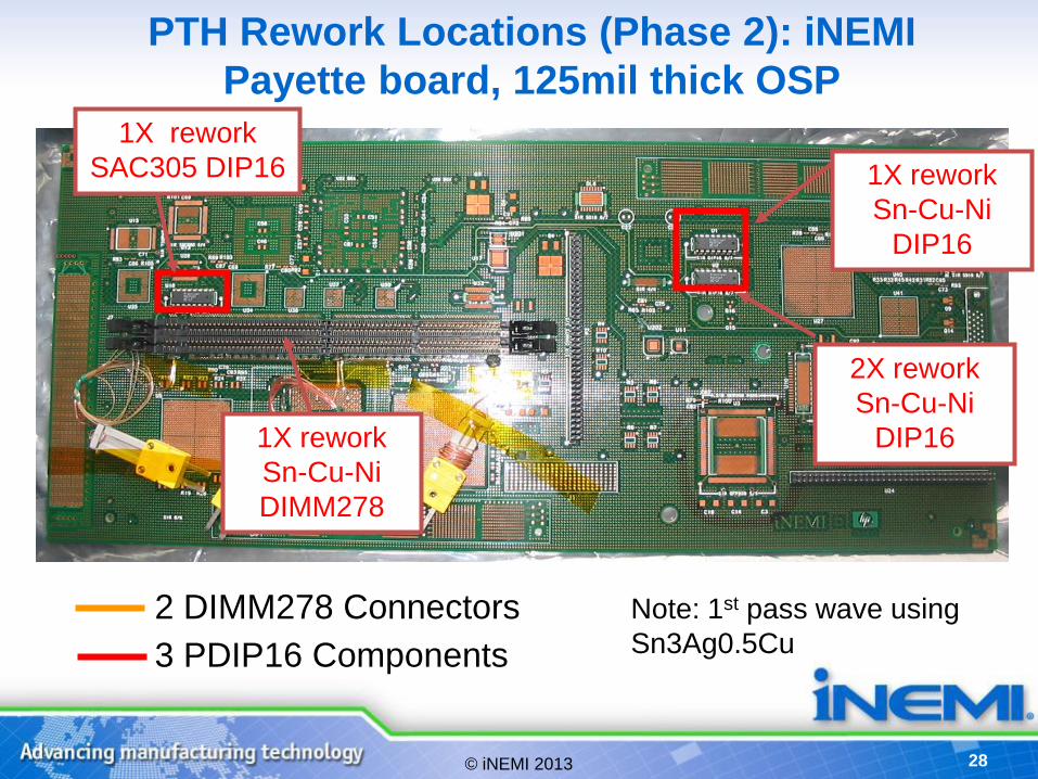
PTH Rework Locations (Phase 2): iNEMI
Payette board, 125mil thick OSP
2 DIMM278 Connectors
3 PDIP16 Components
Note: 1st pass wave using
Sn3Ag0.5Cu
1X rework
Sn-Cu-Ni
DIP16
2X rework
Sn-Cu-Ni
DIP16
1X rework
SAC305 DIP16
1X rework
Sn-Cu-Ni
DIMM278

29 © iNEMI 2013
Mini-pot Rework Status (Phase 1 & 2)
• Further optimization of DIMM and PDIP rework process steps completed.
– Use of laminar flow well (center baffle rework nozzle) suggested and used
to reduce Cu dissolution
– Convection(batch oven) vs. Infrared (In-line) preheat studied: In-line
preheat helped preheat the board faster with less heat loss prior to rework
– Responses measured: dwell time, Cu dissolution, barrel fill & other defects
• Number of difficulties during DIMM connector rework (using Sn-Cu-Ni
alloy) which required further attention.
– Establishing adequate barrel fill (50% for ground connections), while
controlling level of Cu dissolution
Phase 2
30 © iNEMI 2013
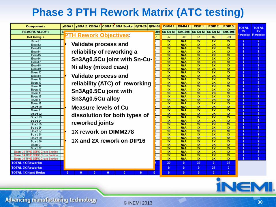
Phase 3 PTH Rework Matrix (ATC testing)
PTH Rework Objectives:
• Validate process and
reliability of reworking a
Sn3Ag0.5Cu joint with Sn-Cu-
Ni alloy (mixed case)
• Validate process and
reliability (ATC) of reworking
Sn3Ag0.5Cu joint with
Sn3Ag0.5Cu alloy
• Measure levels of Cu
dissolution for both types of
reworked joints
• 1X rework on DIMM278
• 1X and 2X rework on DIP16

31 © iNEMI 2013 31
– Phase 3 PDIP16 Rework
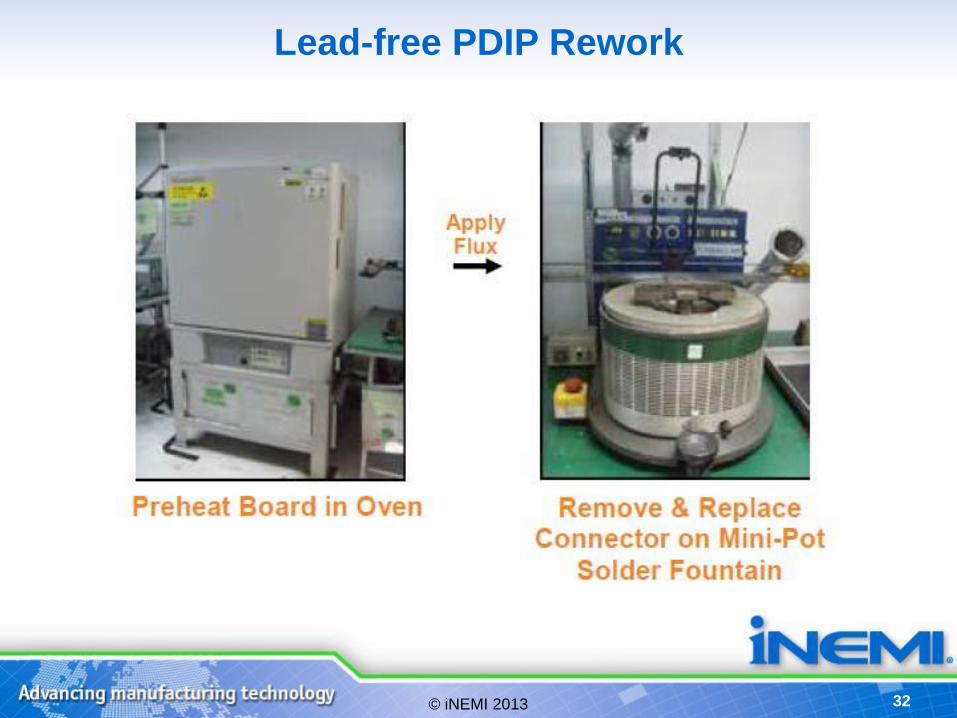
32 © iNEMI 2013
Lead-free PDIP Rework
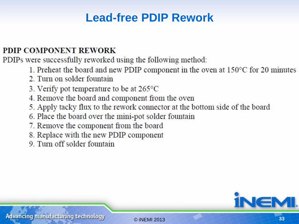
33 © iNEMI 2013
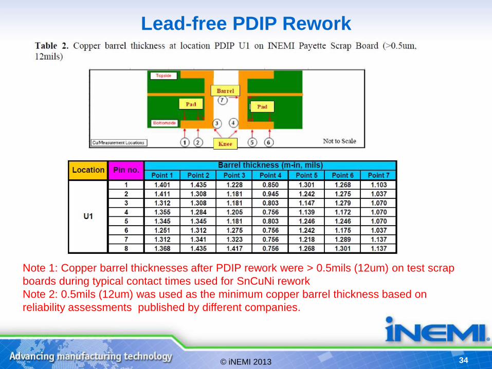
Lead-free PDIP Rework
34 © iNEMI 2013
Lead-free PDIP Rework
Note 1: Copper barrel thicknesses after PDIP rework were > 0.5mils (12um) on test scrap
boards during typical contact times used for SnCuNi rework
Note 2: 0.5mils (12um) was used as the minimum copper barrel thickness based on
reliability assessments published by different companies.
35 © iNEMI 2013
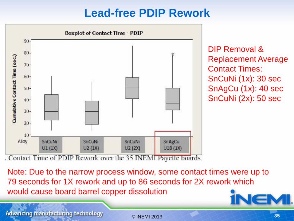
Lead-free PDIP Rework
DIP Removal &
Replacement Average
Contact Times:
SnCuNi (1x): 30 sec
SnAgCu (1x): 40 sec
SnCuNi (2x): 50 sec
Note: Due to the narrow process window, some contact times were up to
79 seconds for 1X rework and up to 86 seconds for 2X rework which
would cause board barrel copper dissolution
36 © iNEMI 2013 36
– Phase 3 DIMM278 Rework
37 © iNEMI 2013
•Experiments were conducted to understand the
affect of board preheat on mini-pot rework using
three different board preheat processes.
37
Effect of Board Preheat on Mini-pot Rework
38 © iNEMI 2013
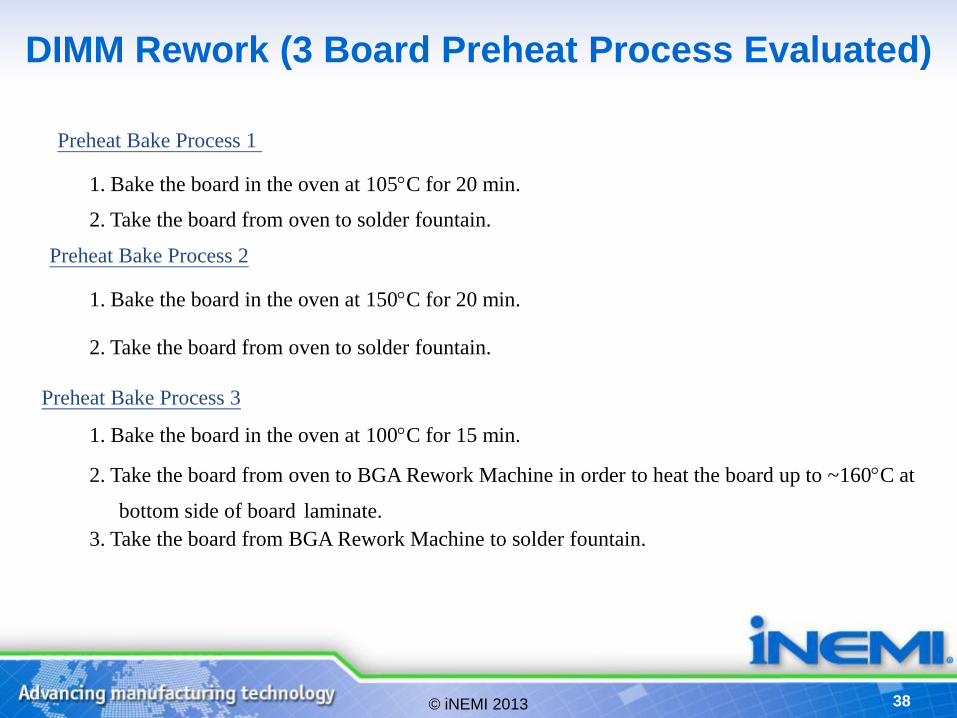
Preheat Bake Process 2
1. Bake the board in the oven at 105C for 20 min.
2. Take the board from oven to solder fountain.
Preheat Bake Process 3
1. Bake the board in the oven at 100C for 15 min.
2. Take the board from oven to BGA Rework Machine in order to heat the board up to ~160C at
bottom side of board laminate.
3. Take the board from BGA Rework Machine to solder fountain.
Preheat Bake Process 1
1. Bake the board in the oven at 150C for 20 min.
2. Take the board from oven to solder fountain.
DIMM Rework (3 Board Preheat Process Evaluated)

39 © iNEMI 2013
Lead-free DIMM Rework Evaluation Stages
+ BGA Rework 160C

40 © iNEMI 2013
Open
do
or
Open
do
or
Open
do
or
Open
do
or
Open
do
or
TCs 1200 1500 1800 2100 2400 Peak
(B) J7_left joint 135 135 134 133 132 255
(B) J7_center joint 137 138 137 136 135 269
(B) J7_right joint 139 139 139 138 136 251
(T) J7_left joint 135 135 134 132 132 232
(T) J7_right joint 139 139 138 137 136 230
(B) J8_center joint 136 137 136 135 134 257
(B) Laminate 2 136 136 135 134 133 167
(B) Laminate 1 135 135 135 134 133 267
(T) Laminate 1 140 140 139 138 137 141
Time at (seconds)
Reflow Profile for Process 2 (Batch Oven Bake, 150°C)
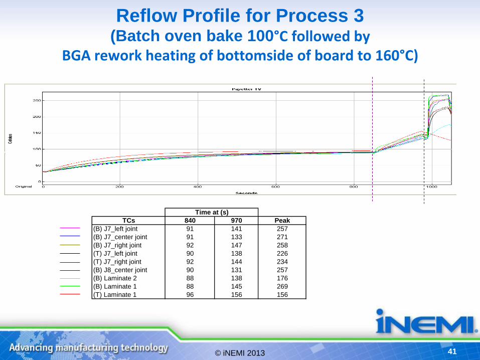
41 © iNEMI 2013
TCs 840 970 Peak
(B) J7_left joint 91 141 257
(B) J7_center joint 91 133 271
(B) J7_right joint 92 147 258
(T) J7_left joint 90 138 226
(T) J7_right joint 92 144 234
(B) J8_center joint 90 131 257
(B) Laminate 2 88 138 176
(B) Laminate 1 88 145 269
(T) Laminate 1 96 156 156
Time at (s)
Reflow Profile for Process 3 (Batch oven bake 100°C followed by
BGA rework heating of bottomside of board to 160°C)
42 © iNEMI 2013
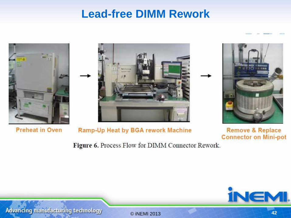
Lead-free DIMM Rework
43 © iNEMI 2013
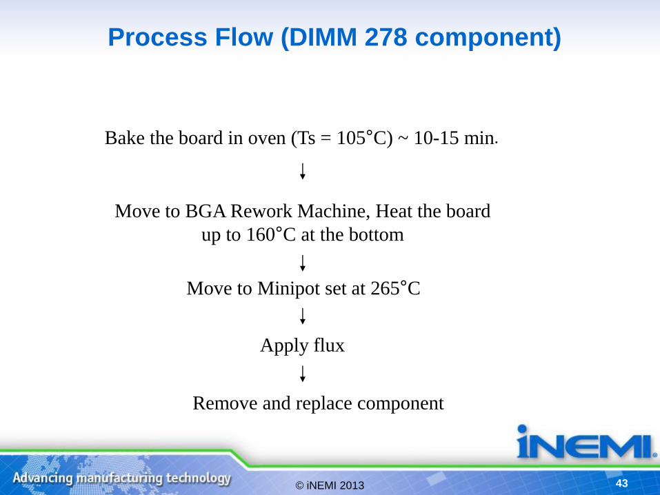
Process Flow (DIMM 278 component)
Bake the board in oven (Ts = 105°C) ~ 10-15 min.
Move to BGA Rework Machine, Heat the board
up to 160°C at the bottom
Move to Minipot set at 265°C
Remove and replace component
Apply flux
44 © iNEMI 2013
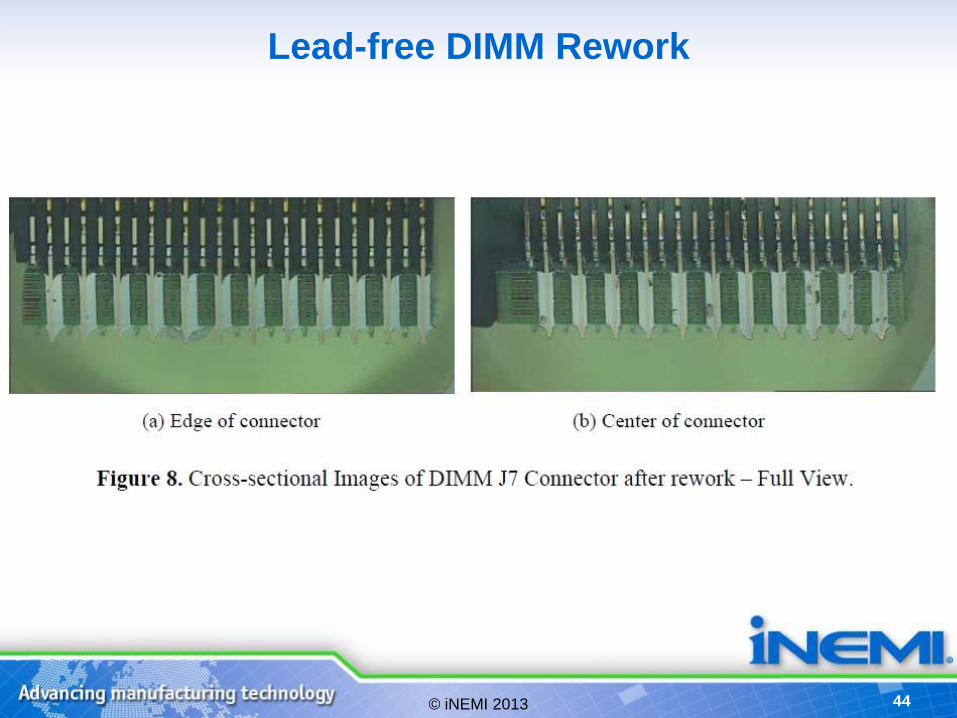
Lead-free DIMM Rework
45 © iNEMI 2013
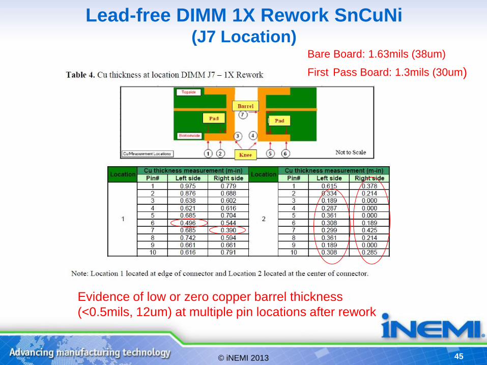
Lead-free DIMM 1X Rework SnCuNi (J7 Location)
Evidence of low or zero copper barrel thickness
(<0.5mils, 12um) at multiple pin locations after rework
Bare Board: 1.63mils (38um)
First Pass Board: 1.3mils (30um)

46 © iNEMI 2013
Lead-free DIMM Rework (Contact times)
Average contact time for DIMM
Removal and Replacement
(SnCuNi):
27 seconds
Note: Due to the narrow process window, some contact times were up to 46
seconds which would cause increased board barrel copper dissolution after
rework
47 © iNEMI 2013
Assembly and Rework Phase 3 Conclusions
• For the 1st pass assembly build no real issues apart from
lead-free wave holefill issues on some of the DIMM 278
connectors on the 125 mil thick OSP board.
• For rework, no real issues during the BGA socket and uBGA
rework.
• More issues during mini-pot wave rework for the DIP and
DIMM component particularly for DIMM rework.
– Copper dissolution and lead-free wave rework holefill were areas
of concern.
48 © iNEMI 2013 48
www.inemi.org Email contacts:
David Godlewski
Grace O'Mallley


![Lead-to-Sales Optimization in retail banking [Dutch]](https://img.pdfslide.us/doc/110x75/55d55d6ebb61ebdd6c8b45ed/lead-to-sales-optimization-in-retail-banking-dutch.jpg)