Embed Size (px)
Citation preview

IP-SPARTAN2E
INDUSTRY PACK
XILINX
HARDWARE REFERENCE MANUAL
Revision 1.0 August 2005
This Document shall not be duplicated, nor its contents used for any purpose, unless express permission has been granted in advance.
ALPHI TECHNOLOGY CORP.
6202 S. Maple Avenue #120 Tempe, AZ 85283 USA Tel : (480) 838 - 2428 Fax: (480) 838 - 4477

ALPHI TECHNOLOGY CORP. page 2 REV 1.0 Part Number: 812-10-001-4000 Copyright ALPHI Technology Corporation, 2005 8/2/2006
TABLE OF CONTENTS
1 Introduction:....................................................................................................................................4 1.1 Functional description: ........................................................................................................................ 4 1.2 BASIC BLOCK DIAGRAM: ............................................................................................................. 5 1.3 ELECTRICAL BLOCK DIAGRAM: ............................................................................................... 6
2 MAP ADDRESS :............................................................................................................................7 2.1 IDSPACE: ............................................................................................................................................. 7 2.2 IOSPACE:............................................................................................................................................. 8
2.2.1 EPM7160- SPARTAN2e dual addressing registers ...................................................................................... 8 2.2.2 IDEPLD SPARTAN2exx identification part ......................................................................................... 9
2.2.2.1 EPREV EPM7160 revision control ......................................................................................................... 9 2.2.2.2 ICR Initialization Control Register......................................................................................................... 10 2.2.2.3 ISR Init Status Register .......................................................................................................................... 10
2.2.3 IVRx Interrupt Vector Register ................................................................................................................... 11 INTSPACE..................................................................................................................................................... 11 2.3 MEMORY SPACE............................................................................................................................. 11
2.3.1 DPR Timing:.............................................................................................................................................. 12 2.4 SRAM interconnection with SPARTAN2e....................................................................................... 13 2.5 SPARTAN2E Memory Request Lines:............................................................................................. 14 2.6 IPbus interconnection with SPARTAN2e ........................................................................................ 15
3 SPARTAN2e I/O ASSIGNMENT................................................................................................15
4 Jumper’s description:....................................................................................................................17 4.1.1 J1 description............................................................................................................................................. 17 4.1.2 J2 description............................................................................................................................................. 17 4.1.3 J3 description............................................................................................................................................. 17 4.1.4 J4 description............................................................................................................................................. 18 4.1.5 J5 description............................................................................................................................................. 18 4.1.6 J6 description............................................................................................................................................. 18
5 Connectors Description: ...............................................................................................................18 5.1 IP bus interface P1.............................................................................................................................. 19
6 Configuring SPARTAN2e.............................................................................................................20 6.1 Boundary scan mode .......................................................................................................................... 20 6.2 Master serial mode. ............................................................................................................................ 21 6.3 Slave parallel mode. ........................................................................................................................... 22
7 EXTERNAL CLOCK FOR SPARTAN2e.....................................................................................24
8 Timing between EP7160 AND SPARTAN2e ...............................................................................25
9 Additional timing...........................................................................................................................26
10 Testing the IP-SPARTAN2e ......................................................................................................29

ALPHI TECHNOLOGY CORP. page 3 REV 1.0 Part Number: 812-10-001-4000 Copyright ALPHI Technology Corporation, 2005 8/2/2006
10.1 Testing read/write operations on registers. .................................................................................. 29 10.2 Testing write operations on the Memory...................................................................................... 30 10.3 Testing read operations from the Memory................................................................................... 30
Figure 1.1: IP-SPARTAN2E BLOCK DIAGRAM______________________________________________________ 6 Figure 6.1: IP-SPARTAN2e Jumpers and Headers Location ________________ Error! Bookmark not defined. Table 3-1 IDSEL0 SPACE byte content_____________________________________________________________ 7 Table 3-1 IOSPACE MAP __________________________________________________________________________ 9 Table 3-2 SRAM Address and Data to SPARTAN2e connection.____________________________________________ 13 Table 3-3 SRAM Data to SPARTAN2e connection ______________________________________________________ 14 Table 6-4 Jumper Description ____________________________________________________________________ 17 Table 6-5 J1 Description_________________________________________________________________________ 17 Table 6-6 J2 Description_________________________________________________________________________ 17 Table 7-7 Connectors Description_________________________________________________________________ 18 Table 7-1 P1 IPBUS connector ___________________________________________________________________ 19 Table 7-1 JTAG Port P2 ________________________________________________________________________ 20

ALPHI TECHNOLOGY CORP. page 4 REV 1.0 Part Number: 812-10-001-4000 Copyright ALPHI Technology Corporation, 2005 8/2/2006
1 Introduction:
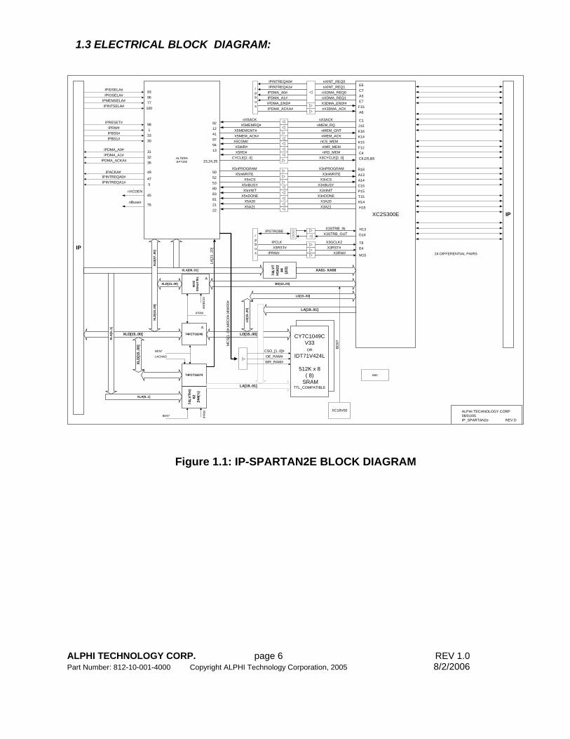
1.1 Functional description: The SPARTAN2E module is populated with a Spartan IIE XC2Sxx embedded programmable FPGA. A wide range of Spartan packages can be selected. Altera EPM7160 is used to provide all the timings and interface between the IPBUS, Spartan chip and the 2Mbytes of Dual Access Memory. Key Features are:
• 48 selectable I/O. • Each line can be selected as an I/O line. • UP TO 2Mbytes of Dual Ported SRAM. • 8 or 32 MHz clock. • 2 interrupts and 2 DMA. • SelectMAP Configuration: Passive Parallel Asynchronous Configuration Via IP Bus. • Device Configuration: XC18v, XC17v. • Passive Serial configuration: Configuration via HW-USB and HW-PCi cables.
The IP-SPARTAN2E uses two chips:
• An EPM7160 chip is used for all timing related to the IPBUS, DPR, SPARTAN2E. • An SPARTAN2E-XC2S300-10 chip.
Interconnection between the DPR and the SPARTAN2E is provides. An optional crystal allows the user to run the SPARTAN2E at a different speed than the IPBUS. Customer must have XILINX development tools to implement their own design. Rev B can be used as stand-alone module.
1. Programming can be achieve through : • The IPbus. • The JTAG. • EEprom.

ALPHI TECHNOLOGY CORP. page 5 REV 1.0 Part Number: 812-10-001-4000 Copyright ALPHI Technology Corporation, 2005 8/2/2006
1.2 BASIC BLOCK DIAGRAM:
ALTERAEPM7160
IPBUSCONTROL
ANDARBITRATION
SPARTAN2E 48 selectable I/O
DUAL PORT RAM
2MBytes
The IP-SPARTAN2E is divided into 3 blocks:
1- The EPM7160 E2 based FPGA that is used for the control of the IPBus and arbitration for the Dual Port Ram. The signals (CS,RD,WR) for the DPR are generated by the EPM7160.
2- The Dual Port Ram 2MX16 SRAM that can be written and Read from The IpBus and the
SPARTAN2E. The arbitration and the request for the bus has been Taking care of via the FPGA that is programmed by factory
3- The Dual Port Ram has been controlled by the FPGA on Board. That process will allow the user to access the ram from the IP bus and the SPARTAN2E without user intervention with the arbitration. All Arbitration between the IPbus and the SPARTAN2E has been implemented within the EPM7160.
ALPHI TECHNOLOGY CORP. page 6 REV 1.0 Part Number: 812-10-001-4000 Copyright ALPHI Technology Corporation, 2005 8/2/2006
1.3 ELECTRICAL BLOCK DIAGRAM:
X5A20 X3A20X5A21 X3A21
X5nINIT X3nINIT
ALPHI TECHNOLOGY CORP08/01/05IP_SPARTAN2e REV D
IP
XLD[15..00]
ALTERAEP7160
XLA[06..01] XA01- XA06
CY7C1049CV33
OR
IDT71V424L
512K x 8( 8)
SRAMTTL_COMPATIBLE
XLA[6..1]
IPXC2S300E
XLD
[15.
.00]
XLD
[07.
.00]
BD[15..00]
LD[15..00]
LA[19..01]
IPDMA_A0# nXDMA_REQ0IPINTREQA1# nXINT_REQ1IPINTREQA0# nXINT_REQ0
CYCLE[2..0] X3CYCLE[2..0]
X5MEM_ACK# nMEM_ACK
IPDMA_A1# nXDMA_REQ1
IPDMA_ACKA# nX3DMA_ACKIPDMA_END# X3DMA_ENDI#
X5MEMRQ# nMEM_RQX5MEMGNT# nMEM_GNT
X5CSM# nCS_MEM
74FCT16245
XLD
[15.
.00]
74LV
TH1
6224
4(½
)
BEN*
BEN*
LACHAD
IPRW
74FCT16374
XC
DE
N#
LD[15..00]
LA[19..01]
LD[1
5..0
0]
X5WR# nWR_MEM
nX5ACK nX3ACK
X5RD# nRD_MEM
osc74LVTH
162245XLD[15..00]
XLA
[6..1
]
A
A
74LV
TH
1622
44 (2/2
)
XC18V00
X5nPROGRAM X3nPROGRAMX5nWRITE X3nWRITE
X5nCS X3nCSX5nBUSY X3nBUSY
BD07
CSO_[1..0]#OE_RAM#WR_RAM#
MC
S[1.
.0]#
,MR
D0#
,MW
R0#
IPIDSELA#IPIOSELA#
IPMEMSELA#IPINTSELA#
IPRESET#IPRW#IPBS0#IPBS1#
IPDMA_A0#IPDMA_A1#
IPDMA_ACKA#
IPINTREQA0#IPINTREQA1#
ipbus
IPRW# X3RW#
IPCLK X3GCLK2X5RST# X3RST#
X3STRB_INX3STRB_OUT
IPSTROBEipbus
X5nDONE X3nDONE
LA[2
1..2
0]
24 DIFFERENTIAL PAIRS
939677100
98
32
30331
31
36
475
45nXCDEN
80535250
979413
23,24,25
411292
83812122
IPACKA# 49R16
C6,D5,B5
F12K15K14K16J15C1
A6F15E7A3C7E6
H15H14T15P15C15A14A13
E4T8
G14H13
M15
C4
nBusen76
IPR
W
Figure 1.1: IP-SPARTAN2E BLOCK DIAGRAM

ALPHI TECHNOLOGY CORP. page 7 REV 1.0 Part Number: 812-10-001-4000 Copyright ALPHI Technology Corporation, 2005 8/2/2006
2 MAP ADDRESS : The IP-SPARTAN2E module uses the three available spaces defined in the Industry Pack specifications.
2.1 IDSPACE:
Up to 32 bytes of registered data provides information about the module to the User. The lower address contains data related to the type of module, revision, etc. Only ODD addresses are valid in byte read mode.
ID space address
Description Value
$01 ASCII “I” $49 $03 ASCII “P” $50 $05 ASCII “A” $41 $07 ASCII “H” $48 $09 Manufacturer identification $11 $0B Module type $19 $0D Revision module $20 $0F Reserved $00 $11 Driver ID,low byte $13 Driver ID,high byte $15 Number of bytes used $0C $17 CRC $19-$3F User space
Table 2-1 IDSEL0 SPACE byte content
ALPHI TECHNOLOGY CORP. page 8 REV 1.0 Part Number: 812-10-001-4000 Copyright ALPHI Technology Corporation, 2005 8/2/2006
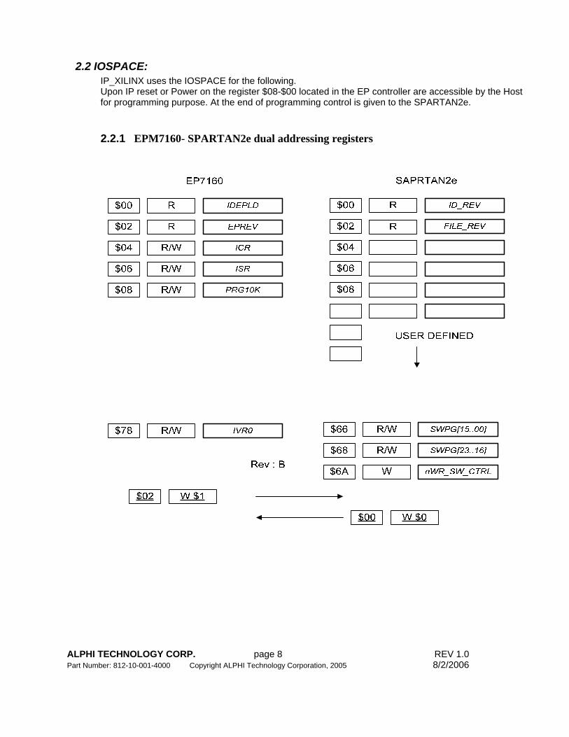
2.2 IOSPACE: IP_XILINX uses the IOSPACE for the following.
Upon IP reset or Power on the register $08-$00 located in the EP controller are accessible by the Host for programming purpose. At the end of programming control is given to the SPARTAN2e.
2.2.1 EPM7160- SPARTAN2e dual addressing registers
ALPHI TECHNOLOGY CORP. page 9 REV 1.0 Part Number: 812-10-001-4000 Copyright ALPHI Technology Corporation, 2005 8/2/2006
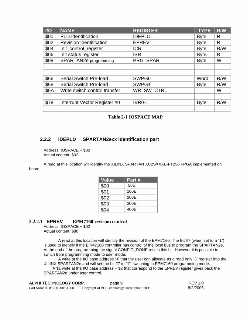
I/O NAME REGISTER TYPE R/W $00 PLD Identification IDEPLD Byte R $02 Revision Identification EPREV Byte R $04 Init_control_register ICR Byte R/W $06 Init status register ISR Byte R $08 SPARTAN2e programming PRG_SPAR Byte W $66 Serial Switch Pre-load SWPG0 Word R/W $68 Serial Switch Pre-load SWPG1 Byte R/W $6A Write switch control transfer WR_SW_CTRL W $78 Interrupt Vector Register #0 IVR0-1 Byte R/W
Table 2-1 IOSPACE MAP
2.2.2 IDEPLD SPARTAN2exx identification part Address: IOSPACE + $00 Actual content: $02
A read at this location will identify the XILINX SPARTAN XC2SXXXE-FT256 FPGA implemented on board.
Value Part # $00 50E
$01 100E $02 200E
$03 300E $04 400E
2.2.2.1 EPREV EPM7160 revision control Address: IOSPACE + $02 Actual content: $80
A read at this location will identify the revision of the EPM7160. The Bit #7 (when set to a “1”)
is used to identify if the EPM7160 controller has control of the local bus to program the SPARTAN2e. At the end of the programming the signal CONFIG_DONE resets this bit. However it is possible to switch from programming mode to user mode. A write at the I/O base address $0 that the user can allocate as a read only ID register into the XILINX SPARTAN2e and will set the bit #7 to “1” ‘switching to EPM7160 programming mode.
A $1 write at the I/O base address + $2 that correspond to the EPREV register gives back the SPARTAN2e under user control.

ALPHI TECHNOLOGY CORP. page 10 REV 1.0 Part Number: 812-10-001-4000 Copyright ALPHI Technology Corporation, 2005 8/2/2006
Value Revision $00 Rev. A $01 Rev. B $02 Rev. C
2.2.2.2 ICR Initialization Control Register Address: IOSPACE + $04
BD03 BD02 BD01 BD00 - - nCONFIG nCONFIG_EN
BD07 BD06 BD05 BD04 DEV_CLRn DEV_OE DEV_CLRn_EN DEV_OE_EN
Bit 0: nCONFIG_EN:
This bit enables a tri-state buffer that controls the nCONFIG line of the SPARTAN2e upon reset the buffer is tri-state. Programming of the nCONFIG line can occur only if the MSEL0 and MSEL1 lines are pulled to VCC
(remove jumpers from J2).
Bit 1: nCONFIG: This bit is use to control the nCONFIG line of the SPARTAN2e
Bit 2: Not used Bit 3:Not used Bit 4: DEV_OE_EN:
This bit enables a tri-state buffer that control the DEV_OE line of the SPARTAN2e Bit 5: DEV_CLR_EN:
This bit enables a tri-state buffer that control the DEV_CLRn line of the SPARTAN2e
Bit 6: DEV_OE: This bit can be use to control the DEV_OE line of the SPARTAN2e
Bit 7: DEV_CLRn: This bit can be use to control the DEV_CLRn line of the SPARTAN2e
2.2.2.3 ISR Init Status Register Address: IOSPACE + $06
This Register provides the status of SPARTAN2e programming lines

ALPHI TECHNOLOGY CORP. page 11 REV 1.0 Part Number: 812-10-001-4000 Copyright ALPHI Technology Corporation, 2005 8/2/2006
BD03 BD02 BD01 BD00 RDYnBSY CONF_DONE nSTATUS nCONFIG
BD07 BD06 BD05 BD04 Msel1 Msel0 INIT_DONE CONF_STAT
Bit 0: nCONFIG This bit when set indicates that the SPARTAN2e Configuration started.
Upon Reset this bit is set pull high by a pull-up resistance to allow multiple possibilities of programming, else this line is low in theory.
Bit 1: nSTATUS Bit 2: CONF_DONE Bit 3: RDYnBSY Bit 4: CONF_STAT Bit 5: INIT_DONE Bit 7, 6: MSEL [1..0]
MSEL[1..0] Description 00 Master serial mode 10 Slave parallel mode 11 Slave serial mode
2.2.3 IVRx Interrupt Vector Register Address: IOSPACE + $78
This eight bit register located at address IOSPACE + $78 can be read and written by the host. The vector is automatically provided upon INTSPACE cycle perform by the host with lower bit # 0 been the “image “of the interrupt,”0” for interrupt # 0. “1” for interrupt # 1.
INTSPACE When the SPARTAN2e has an interrupt pending the carrier module can read the IVR register that has
been program early by the carrier. The ATC_SPARTAN2e supports one interrupt (IRQ0). Interrupt vector is transferred from the SPARTAN2e through a buffer to the IPbus. Upon receiving an interrupt cycle (INTSELA) an Interrupt vector register is provided.
2.3 MEMORY SPACE Up to 2Mbytes of SRAM is mapped into the Memory space. The SRAM can be set to
ALPHI TECHNOLOGY CORP. page 12 REV 1.0 Part Number: 812-10-001-4000 Copyright ALPHI Technology Corporation, 2005 8/2/2006
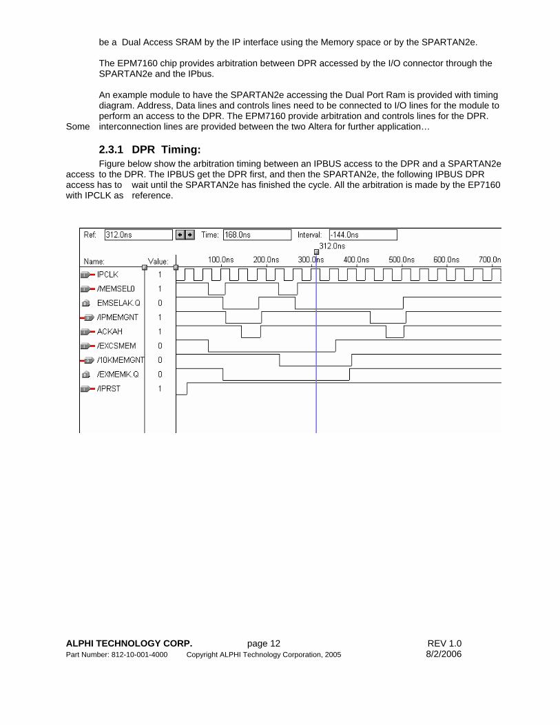
be a Dual Access SRAM by the IP interface using the Memory space or by the SPARTAN2e. The EPM7160 chip provides arbitration between DPR accessed by the I/O connector through the SPARTAN2e and the IPbus. An example module to have the SPARTAN2e accessing the Dual Port Ram is provided with timing diagram. Address, Data lines and controls lines need to be connected to I/O lines for the module to perform an access to the DPR. The EPM7160 provide arbitration and controls lines for the DPR. Some interconnection lines are provided between the two Altera for further application…
2.3.1 DPR Timing: Figure below show the arbitration timing between an IPBUS access to the DPR and a SPARTAN2e access to the DPR. The IPBUS get the DPR first, and then the SPARTAN2e, the following IPBUS DPR access has to wait until the SPARTAN2e has finished the cycle. All the arbitration is made by the EP7160 with IPCLK as reference.

ALPHI TECHNOLOGY CORP. page 13 REV 1.0 Part Number: 812-10-001-4000 Copyright ALPHI Technology Corporation, 2005 8/2/2006
2.4 SRAM interconnection with SPARTAN2e
A separation is provided between the IPbus connected to the SPARTAN2e and the LD bus connected to the dual ported memory providing faster access. The IPbus can access concurrently registers located within the SPARTAN2e while the SPARTAN2e is accessing the Dual shared memory. Arbitration between the IPbus accessing the Dual ported memory and the SPARTAN2e accessing the also the Dual ported memory remains the same on the two revision.
SRAM ADDRESS SPARTAN
2e PIN Description
LA01 C16 Lower Address Line LA02 D16 LA03 D15 LA04 E13 LA05 E16 LA06 F13 LA07 F16 LA08 A9 LA09 A10 LA10 A11 LA11 A12 LA12 B9 LA13 B10 LA14 B11 LA15 B12 LA16 C9 LA17 C10 LA18 C11 LA19 C12 Higher Address Line
Table 2-2 SRAM Address and Data to SPARTAN2e connection.

ALPHI TECHNOLOGY CORP. page 14 REV 1.0 Part Number: 812-10-001-4000 Copyright ALPHI Technology Corporation, 2005 8/2/2006
SRAM DATA SPARTAN2e PIN
Description
LD00 D1 Lower Data Line LD01 D3 LD02 A5 LD03 E1 LD04 H1 LD05 B4 LD06 G5 LD07 B3 LD08 F5 LD09 F3 LD10 G3 LD11 H3 LD12 E3 LD13 A4 LD14 D2 LD15 A7 Higher Data Line
Table 2-3 SRAM Data to SPARTAN2e connection
2.5 SPARTAN2E Memory Request Lines:
Signal Name SPARTAN2e PIN
Description Type
nMEM_GNT K16 SPARTAN receive granted Access to DPR
Input
nMEM_REQ J15 SPARTAN Memory request. Must stay low until end of cycle. Re-sync with IPCLK (GCLK1) before arbitration.
Output
nMEM_ACK K14 SPARTAN Acknowledge. Not used .See Note.
Output
nCS_MEM K15 SPARTAN Chip selects Memory. Feed the EP7160 that will direct the signal to the CS_DPR without delay.
Output
nRD_MEM C4 SPARTAN Read signal for DPR.Same as above
Output
nWR_MEM F12 SPARTAN Write signal for DPR.Same as above
Output
nX3RW M15 Image of the IPRW signal from the IPbus
Input

ALPHI TECHNOLOGY CORP. page 15 REV 1.0 Part Number: 812-10-001-4000 Copyright ALPHI Technology Corporation, 2005 8/2/2006
Note: This signal is used as acknowledge only with a particular test where the IPBUS read or write to the DPR through the SPARTAN2e using the arbitration process. In this case the EP7160 does not provide the IPACK automatically but wait for the nX3ACK from the SPARTAN2e. Address I/O base +$7E is used.
2.6 IPbus interconnection with SPARTAN2e
Signal Name SPARTAN2e PIN
Description Type
nDMAREQ0 A3 IP DMA REQ0 Output nDMAREQ1 E7 IP DMA REQ2 Output nINTREQ0 E6 IP INT. REQ 0 Output nINTREQ1 C7 IP INT. REQ 1 Output nIPDS0 H13 DATA STROBE 0 Input nIPDS1 G14 DATA STROBE 1 Input IPRW M15 IPBUS READ/WRITE Input nIPRST E4 IPBUS RESET Input IPCLK T8 IPBUS CLOCK 8/32MHZ Input XA01 L14 IPBUS ADDRESS LINE Input XA02 L12 IPBUS ADDRESS LINE Input XA03 K13 IPBUS ADDRESS LINE Input XA04 J16 IPBUS ADDRESS LINE Input XA05 E16 IPBUS ADDRESS LINE Input XA06 G12 IPBUS ADDRESS LINE Input nDMAACK A6 IP DMA ACKNOWLEDGE Input nDMAEND F15 IP DMA END Input
3 SPARTAN2e I/O ASSIGNMENT CLOCKS:
Signal Name SPARTAN2e PIN
Description Type
GCLK1(IPCLK) T8 IPBUS CLOCK (32 OR 8 MHz)
Input
GCLK2(OSC_IN) B8 User Clock if Populated on IC9 location
Input
Note: GCLK2 is also connected to the pin CLKUSER( PIN B8). See paragraph EXTERNAL CLOCK FOR SPARTAN2e

ALPHI TECHNOLOGY CORP. page 16 REV 1.0 Part Number: 812-10-001-4000 Copyright ALPHI Technology Corporation, 2005 8/2/2006
I/O PIN
XILINX pin Name I/O name J1 EX_LDP0 Pin 1 L1 EX_LDP1 Pin 2 R4 EX_LDP2 Pin 3 P1 EX_LDP3 Pin 4 P6 EX_LDP4 Pin 5 K4 EX_LDP5 Pin 6 J2 EX_LDP6 Pin 7 L4 EX_LDP7 Pin 8 N2 EX_LDP8 Pin 9 M3 EX_LDP9 Pin 10 T3 EX_LDP10 Pin 11 K2 EX_LDP11 Pin 12 N5 EX_LDP12 Pin 13 L3 EX_LDP13 Pin 13 R7 EX_LDP14 Pin 13 M1 EX_LDP15 Pin 13
XILINX pin Name I/O name K1 EX_LDN0 Pin 1 L2 EX_LDN1 Pin 2 P4 EX_LDN2 Pin 3 P2 EX_LDN3 Pin 4 N6 EX_LDN4 Pin 5 K5 EX_LDN5 Pin 6 J3 EX_LDN6 Pin 7 L5 EX_LDN7 Pin 8 N3 EX_LDN8 Pin 9 M4 EX_LDN9 Pin 10 T4 EX_LDN10 Pin 11 K3 EX_LDN11 Pin 12 P5 EX_LDN12 Pin 13 M2 EX_LDN13 Pin 13 T7 EX_LDN14 Pin 13 N1 EX_LDN15 Pin 13

ALPHI TECHNOLOGY CORP. page 17 REV 1.0 Part Number: 812-10-001-4000 Copyright ALPHI Technology Corporation, 2005 8/2/2006
Spare pins Between FPGA and SPARTAN2E for custom use:
Signal Name SPARTAN2e PIN
Description Type
X3IOXILINX C2 Input
4 Jumper’s description:
Jumpers Description J1 STROB signals J2 Supply Voltage selection for bank4 of SPARTAN2e J3 Supply Voltage selection for bank6 of SPARTAN2e J4 Supply Voltage selection for bank5 of SPARTAN2e J5 Control line for the Xilinx serial EPROM J6 SPARTAN2e Programming Mode selection : MSEL0 ,MSEL1 and MSEL2 J7 TDI & TDO selection
Table 4-4 Jumper Description
4.1.1 J1 description
Jumpers Pin Description J1 1-2 The strobe signal will be used as an output. J1 2-3 The strobe signal will be used as an input.
Table 4-5 J1 Description
4.1.2 J2 description
Jumpers Pin Description J2 1-2 Supply 3.3v to bank 4 J2 2-3 Supply 2.5v to bank 4
Table 4-6 J2 Description
4.1.3 J3 description
Jumpers Pin Description J2 1-2 Supply 3.3v to bank 6 J2 2-3 Supply 2.5v to bank 6
Table 4-7 J3 Description

ALPHI TECHNOLOGY CORP. page 18 REV 1.0 Part Number: 812-10-001-4000 Copyright ALPHI Technology Corporation, 2005 8/2/2006
4.1.4 J4 description
Jumpers Pin Description J2 1-2 Supply 3.3v to bank 5 J2 2-3 Supply 2.5v to bank 5
Table 4-8 J4 Description
4.1.5 J5 description
Jumpers Pin Description J2 1-2 Enabling Xilinx serial EPROM J2 2-3 Supply 2.5v to bank 5
Table 4-9 J5 Description
4.1.6 J6 description
Jumpers Pin Description J2 5-6 ON
3-4 ON MSEL0 & MSEL1 are Pulled Low (Grounded) SPARTAN2e Configuration Data source Master Serial
J2 5-6 OFF 3-4 OFF
MSEL0 & MSEL1 are Pulled High (VCC) SPARTAN2e Configuration Data source slave serial
J2 5-6 OFF 3-4 ON
MSEL0 Low & MSEL1 (VCC) SPARTAN2e Configuration Data source IP Bus for SelectMAP configuration
J2 5-6 ON 3-4 OFF
MSEL1 Low & MSEL0 (VCC) SPARTAN2e Configuration Data source Boundary scan
Table 4-10 J6 Description
5 Connectors Description:
CONNECTOR DESCRIPTION P1 Factory Use : Control PLD Configuration P2 SPARTAN2e configuration using JTAG connector
Table 5-7 Connectors Description

ALPHI TECHNOLOGY CORP. page 19 REV 1.0 Part Number: 812-10-001-4000 Copyright ALPHI Technology Corporation, 2005 8/2/2006
5.1 IP bus interface P1
P1 Pin 1 GND Pin 26 GND Pin 2 +5V Pin 27 +5V Pin 3 IPRESET* Pin 28 IPRW* Pin 4 XLD00 Pin 29 IDSEL0* Pin 5 XLD01 Pin 30 DMAREQ0* Pin 6 XLD02 Pin 31 MEMSEL0* Pin 7 XLD03 Pin 32 DMAREQ1* Pin 8 XLD04 Pin 33 INTESEL0* Pin 9 XLD05 Pin 34 DMACK* Pin 10 XLD06 Pin 35 IOSEL0* Pin 11 XLD07 Pin 36 Pin 12 XLD08 Pin 37 XLA1 Pin 13 XLD09 Pin 38 DMAEND* Pin 14 XLD10 Pin 39 XLA02 Pin 15 XLD11 Pin 40 ERROR* Pin 16 XLD12 Pin 41 XLA03 Pin 17 XLD13 Pin 42 INTREQ0* Pin 18 XLD14 Pin 43 XLA04 Pin 19 XLD15 Pin 44 INTREQ1* Pin 20 IPBS0* Pin 45 XLA05 Pin 21 IPBS1* Pin 46 Strobe* Pin 22 Pin 47 XLA06 Pin 23 Pin 48 IPACK* Pin 24 +5V Pin 49 +5V Pin 25 GND Pin 50 GND
Table 5-1 P1 IPBUS connector

ALPHI TECHNOLOGY CORP. page 20 REV 1.0 Part Number: 812-10-001-4000 Copyright ALPHI Technology Corporation, 2005 8/2/2006
6 Configuring SPARTAN2e SPARTAN configuration modes are selected using bit 2 of the INITIAL CONTROL REGISTER at $4:
• When bit 2 = “0” the Spartan can be configured using Master Slave and JTAG mode. • When bit 2 = “1” the Spartan can be configured using SELECT MAP mode.
NOTE: M0 & M2 of J6 must be connected to GND.
6.1 Boundary scan mode The SPARTAN2e can be programmed using JTAG connector. Connector P2 provides the interface with the XILINX pod chip.
Pin Signal name Description 1 GND GROUND 2 Vref reference voltage 3 GND GROUND 4 TMS JTAG state machine control 5 GND GROUND 6 TCK Clock signal 7 GND GROUND 8 TDO Data out 9 GND GROUND 10 TDI Data in 11 GND GROUND 12 NC No connect 13 GND GROUND 14 NC No connect
Table 6-1 JTAG Port P2
ALPHI TECHNOLOGY CORP. page 21 REV 1.0 Part Number: 812-10-001-4000 Copyright ALPHI Technology Corporation, 2005 8/2/2006
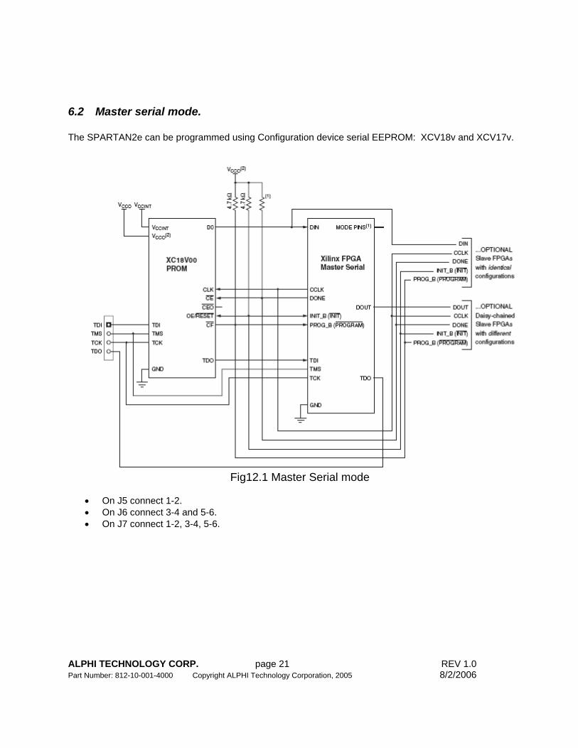
6.2 Master serial mode. The SPARTAN2e can be programmed using Configuration device serial EEPROM: XCV18v and XCV17v.
Fig12.1 Master Serial mode
• On J5 connect 1-2. • On J6 connect 3-4 and 5-6. • On J7 connect 1-2, 3-4, 5-6.

ALPHI TECHNOLOGY CORP. page 22 REV 1.0 Part Number: 812-10-001-4000 Copyright ALPHI Technology Corporation, 2005 8/2/2006
6.3 Slave parallel mode.
Slave Parallel Configuration Circuit Diagram.
Jumper configuration • On J5 connect 2-3.

ALPHI TECHNOLOGY CORP. page 23 REV 1.0 Part Number: 812-10-001-4000 Copyright ALPHI Technology Corporation, 2005 8/2/2006
Loading Configuration Data for the Slave
Parallel Mode Download sequence
1. Start with either IP bus reset or power-up reset. 2. The module should be under EP control.
• Read the revision register at I/O base address+$02. Bit #7 should be set to “1”. With actual revision you should read $80.
• Make a write $0 at I/O base address + $00. The module switches to EP control allowing access to the programming registers.
3. The ICR initialization register located at I/O base address + $4 should read “00”. 4. Write “4” to ICR to enable SELECTMAP mode.
5. Pull nPROGRAM line to GND by writing “1 to ICR register.
ALPHI TECHNOLOGY CORP. page 24 REV 1.0 Part Number: 812-10-001-4000 Copyright ALPHI Technology Corporation, 2005 8/2/2006
• This line is normally the line is Pull-up with a 1k to the VCC.
6. Poll the ISR until the nBUSY bit #0 is low. NOTE: for clock speed less than 50MHZ, there is no need to check BUSY signal.
7. Write the first byte to the Initialization Register located at base I/O address + $8. NOTE: EPLD will drive CS and write signals low when INIT signal goes high.
8. Check that nBUSY line that went high immediately after the write and is back to low before sending
the next data. `
9. Repeat steps 9 to 11 until all bits have been downloaded.
10. Read the ISR and verify that CONF_DONE (bit #2) are high. 11. Write a $1 at the I/O base address + $02 to switch the SPARTAN2e under user control.
12. The EPLD should have release the control of the SPARTAN2e, you should be able now to read the ID
and revision registers of the SPARTAN2e and also accessed all the other registers. NOTE: initially PROGRAM,INIT,WR and CS are set to high. EXAMPLE (in assembly language) IPFPGA IDNT 1,0 START: LEA.L ($FFF58000).L,A0; base register LEA.L ($FFE00000).L,A1; configuration start address LEA.L ($FFEA4922).L,A2;configuration end address LEA.L ($FFF45006).L,A3 MOVE.B #$2,(A0+4); reset cs wr M1 X5PROG MOVE.B #$0,(A0+4); MOVE.B #$4,(A0+4); X5PROG low, M1 high MOVE.B #$1,(A0+4); PROG low MOVE.B #$0,(A0+4); PROG high WRH MOVE.W (A0+6),D0 ANDI.B #$2,D0 BNE.W WRH WRIT MOVE.B (A1)+,(A0+8) MOVE.B #$57,(A3);wr high W CMPA.L A1,A2 BNE.L WRIT MOVE.B #$2,(A0+4); PROG, CS, write, X5PROG high , M1 low TRAP #15 DC.W END
7 EXTERNAL CLOCK FOR SPARTAN2e SPARTAN2e XILINX Setup
1. External oscillator. • Must assign pin B8 to GCLK1 in block of XILINX to have SPARTAN2e use external clock.
2. Internal IP-CLK.
• Must assign pin T8 to GCLK in block of XILINX to have SPARTAN2e use internal clock. XILINX Compilation
ALPHI TECHNOLOGY CORP. page 25 REV 1.0 Part Number: 812-10-001-4000 Copyright ALPHI Technology Corporation, 2005 8/2/2006
1. Important setup note when compiling using CLKUSR pin of the XILINX. • Go to Assign. • Then Device. • Device Options. • In the Individual Device Options select the following. • User-Supplied Start-up Clock (CLKUSR). • Then bottom of box check on both CLKUSR boxes.
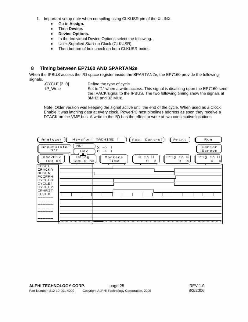
8 Timing between EP7160 AND SPARTAN2e When the IPBUS access the I/O space register inside the SPARTAN2e, the EP7160 provide the following signals. -CYCLE [2..0] Define the type of cycle
-IP_Write Set to “1” when a write access. This signal is disabling upon the EP7160 send the IPACK signal to the IPBUS. The two following timing show the signals at 8MHZ and 32 MHz.
Note: Older version was keeping the signal active until the end of the cycle. When used as a Clock Enable it was latching data at every clock. PowerPC host pipelines address as soon they receive a DTACK on the VME bus. A write to the I/O has the effect to write at two consecutive locations.

ALPHI TECHNOLOGY CORP. page 26 REV 1.0 Part Number: 812-10-001-4000 Copyright ALPHI Technology Corporation, 2005 8/2/2006
9 Additional timing Some additional arbitration timing between IPBUS and SPARTAN2e
EXAMPLE # 1:

ALPHI TECHNOLOGY CORP. page 27 REV 1.0 Part Number: 812-10-001-4000 Copyright ALPHI Technology Corporation, 2005 8/2/2006
ARBITRATION BETWWEN IP BUS MEMORY ACCESS (READ) AND SPARTAN2e MEMORY ACCES (READ). THE IPBUS HAS CONTROL FIRST OF THE DPR THEN THE SPARTAN2e. 10KMEMRQ MUST STAY LOW UNTIL THE END OF THE CYCLE. 10KMEMGNT IS REMOVED TWO CLOCK LATER DUE TO THE 10KMEMRQ FROM THE SPARTAN2e WHICH GET RESYNCHRONIZED WITH THE IPCLK ( 8MHZ) VME162 WITH VME4SIP Note : 10KMEMACK IS GENERATED BUT NOT USED INTO ARBITRATION ALL THE DPR SIGNALS ARE SWITCHED INSIDE THE 7160 CPLD. ALL THESE TEST USE A STATE MACHINE IMPLEMENTED AS EXAMPLE INTO THE SPARTAN2e WITH A 10KMEMRQ GENERATE BY THE GCLK1 CLOCK DIVIDED BY 8. THE TIMING ACCESS OF THE DPR MATCH THE REQUIREMENT OF 70 ns nCS MEMORY ACCESS. USING GCLK1 AT 8MHZ SHOULD BE NO PROBLEM Date: 03-04-05
EXAMPLE # 2: ARBITRATION BETWWEN IP BUS MEMORY ACCESS (READ) AND SPARTAN2e MEMORY ACCES (READ). SAME AS ABOVE EXCEPT THAT THE SPARTAN2e GET THE BUS BEFORE THE IPBUS.

ALPHI TECHNOLOGY CORP. page 28 REV 1.0 Part Number: 812-10-001-4000 Copyright ALPHI Technology Corporation, 2005 8/2/2006
EXAMPLE # 3: ARBITRATION BETWWEN IP BUS MEMORY ACCESS (READ) AND SPARTAN2e MEMORY ACCES (READ). SAME AS EXAMPLE # 1 BUT THE IPBUS GET CONTROL FIRST OF THE DPR THEN THE SPARTAN2e. A WRITE IS PERFORMED BY THE IPBUS

ALPHI TECHNOLOGY CORP. page 29 REV 1.0 Part Number: 812-10-001-4000 Copyright ALPHI Technology Corporation, 2005 8/2/2006
10 Testing the IP-SPARTAN2e Configuration files provided by Alphi technology: “IPSPART.exo” & “ipspart.abs” would allow testing the IP-SPARTAN board.
10.1 Requirements
• Desktop system with DOS interface. • PCPLUS program. • VME162 Motorola carrier. • Parallel to serial Cable. • IP-SPARTAN module.
10.2 Setup
• Connect pins 2&3 of jumper 3. • Load the “IPSPART.exo” file into the VME board by typing the following command:
lo 0 ffe00000 “page up” button the press a (to select to ASCII mode) a:\ipsprat.exo (if the file exists on diskette)
This commends will load the SPARTAN configuration file. Note: “IPSPART.exo” file size is ~14k lines. • Load the “IPSPART.abs” file into the VME board by typing the following command:
lo 0 “page up” button the press a (to select to ASCII mode) a:\ipsprat.abs (if the file exists on diskette)
This commends will load the software that will load the configuration file into SPARTAN using IP interface. • Run the “IPSPART.abs” to load it into the fpga:
g 1000 “W” must be printed to screen indicating that a byte has is written into the Spartan. Note: the board base register address is “fff58000” and memory base address is “800000”.
10.3 Verify Board ID’s • Board ID: at address, should read the following values:
49,50,41,48,11,20,0A,00,00,00,0A,00. • PLD identification: at address 0 of I/O space, should read $02 • Revision identification: at address 2 of I/O space, should read $80.
10.4 Testing read/write operations on registers.
• Switch to the SPARTAN IP by writing “1” address “2” of I/O space. • Go to address “C” of I/O space and write “aaaa”. Note: all access are done using word format. • The same value “aaaa” must appear on address “3C” of I/O space. • Repeat the same procedure for “5555”.

ALPHI TECHNOLOGY CORP. page 30 REV 1.0 Part Number: 812-10-001-4000 Copyright ALPHI Technology Corporation, 2005 8/2/2006
10.5 Testing write operations on the Memory Register side
• Go to address “C” of I/O space and write “0” to enable write operation into the memory from the register.
• Go to address “E” of I/O space and write “aaaa”. • Go to address “10” of I/O space and write “2” to specify the memory address to write to.
Memory Side
• Go to address “xxx4” of memory space. • “aaaa” value must appear. • Repeat the same procedure for “5555”.
10.6 Testing read operations from the Memory Memory Side
• Go to address “xxx6” of memory space. • Write aaaa” value.
Register side
• Go to address “C” of I/O space and write “1” to enable read operation from the memory into the register.
• Go to address “10” of I/O space and write “3” to specify the memory address to read from. • Go to address “48” of I/O space. • “aaaa” must appear. • Repeat the same procedure for “5555”.
Note: to test the Xilinx serial EPROM, pins 1&2 of jumper 3 must be connected together.
10.7 Testing the I/Os
• Go to address “C” of I/O space and write “2” to enable positive I/Os counter. Pulses must appear on the consecutive I/O pins 1 to 16.
• Go to address “C” of I/O space and write “4” to enable negative I/Os counter. Pulses must appear on
the consecutive I/O pins 26 to 41.