Embed Size (px)
Citation preview
1FEATURES APPLICATIONS
DESCRIPTION
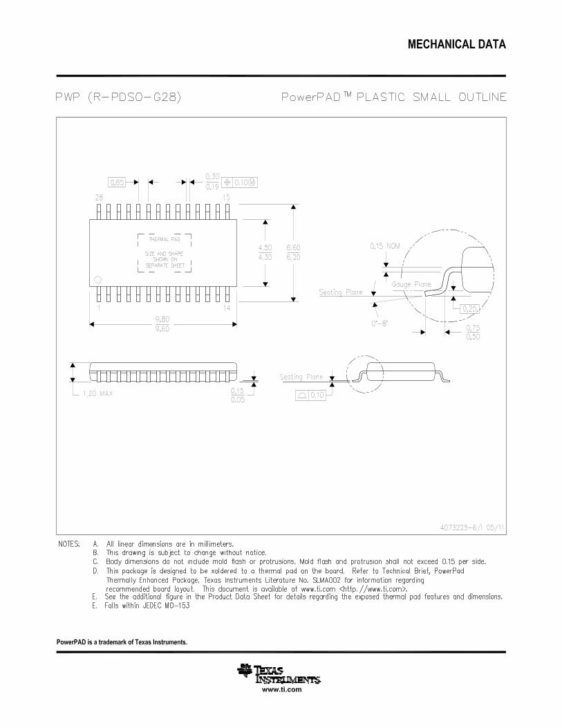
SN65HVS882
www.ti.com ........................................................................................................................................................................................................ SLAS601–MAY 2008
INDUSTRIAL 8-DIGITAL-INPUT SERIALIZER
• Sensor Inputs for Industrial Automation and2• Eight InputsProcess Control– High Input Voltage – up to 34 V
• High Channel Count Digital Input Modules for– Selectable Debounce Filters – 0 ms to 3 ms PC and PLC Systems– Flexible Input Current Limit – 0.2 mA to 5.2 • Decentralized I/O Modules
mA • Motion Control Systems– Field Pins Protected to 15-kV HBM ESD
• Output Drivers for External Status LEDs• Cascadable in Multiples of Eight Inputs• SPI-Compatible Interface• Regulated 5-V Output for External Isolator• Over-Temperature Indicator
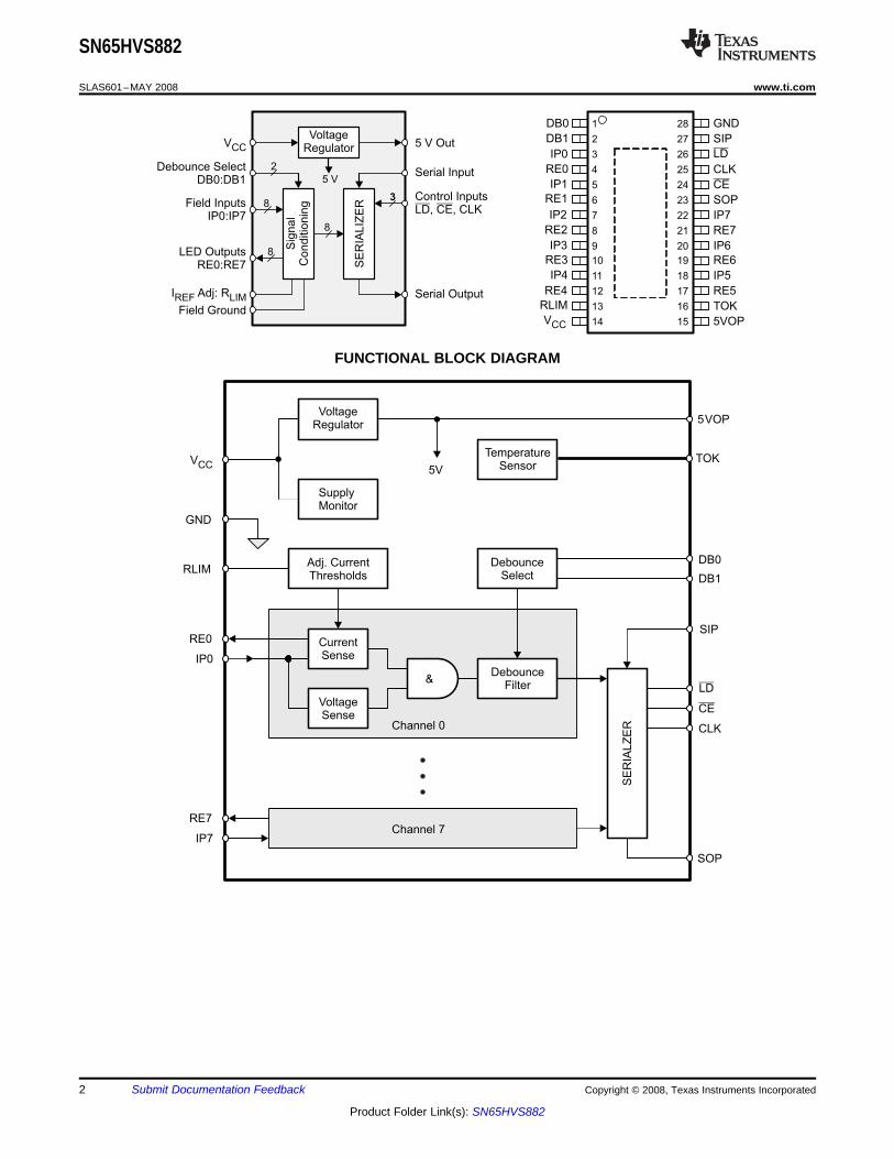
The SN65HVS882 is an eight channel, digital-input serializer for high-channel density digital input modules inindustrial automation. In combination with galvanic isolators the device completes the interface between the highvoltage signals on the field-side and the low-voltage signals on the controller side. Input signals arecurrent-limited and then validated by internal debounce filters.
With the addition of a few external components, the input switching characteristics can be configured inaccordance with IEC61131-2 for Type 1, 2, and 3 sensor switches.
Upon the application of load and clock signals, input data is latched in parallel into the shift register andafterwards clocked out serially.
Cascading of multiple devices is possible by connecting the serial output of the leading device with the serialinput of the following device, enabling the design of high-channel count input modules. Multiple devices can becascaded through a single serial port, reducing both the isolation channels and controller inputs required.
Input status can be visually indicated via constant current LED outputs. The current limit on the inputs is set by asingle external precision resistor. An integrated voltage regulator provides a 5-V output to supply low-powerisolators. An on-chip temperature sensor provides diagnostic information for graceful shutdown and systemsafety.
The SN65HVS882 is available in a 28-pin PWP PowerPAD™ package, allowing for efficient heat dissipation. Thedevice is characterized for operation at temperatures from -40°C to 125°C.
1
Please be aware that an important notice concerning availability, standard warranty, and use in critical applications ofTexas Instruments semiconductor products and disclaimers thereto appears at the end of this data sheet.
2PowerPAD is a trademark of Texas Instruments.
PRODUCTION DATA information is current as of publication date. Copyright © 2008, Texas Instruments IncorporatedProducts conform to specifications per the terms of the TexasInstruments standard warranty. Production processing does notnecessarily include testing of all parameters.
VCC
Debounce SelectDB0:DB1
Field InputsIP0:IP7
LED OutputsRE0:RE7
5 V
8
8
8
3
2
1
2
3
4
5
6
7
8
9
10
11
12
13
14
28
27
26
25
24
23
22
21
20
19
18
17
16
15
GND
SIP
LD
CLK
CE
SOP
IP7
RE7
IP6
RE6
IP5
RE5
TOK
5VOP
DB0
DB1
IP0
RE0
IP1
RE1
IP2
RE2
IP3
RE3
IP4
RE4
RLIM
VCC
I Adj: RREF LIM
Field Ground
5 V OutVoltage
Regulator
Serial Input
Serial Output
SE
RIA
LIZ
ER
Sig
nal
Conditio
nin
g
Control Inputs, , CLKLD CE
VoltageRegulator
TemperatureSensor
SupplyMonitor
Adj. CurrentThresholds
DebounceSelect
CurrentSense
VoltageSense
DebounceFilter
SE
RIA
LZ
ER
&
Channel 0
Channel 7
VCC
GND
RLIM
RE0
IP0
RE7
IP7
5VTOK
SIP
SOP
CLK
LD
CE
DB0
DB1
5VOP
SN65HVS882
SLAS601–MAY 2008 ........................................................................................................................................................................................................ www.ti.com
FUNCTIONAL BLOCK DIAGRAM
2 Submit Documentation Feedback Copyright © 2008, Texas Instruments Incorporated
Product Folder Link(s): SN65HVS882
SN65HVS882
www.ti.com ........................................................................................................................................................................................................ SLAS601–MAY 2008
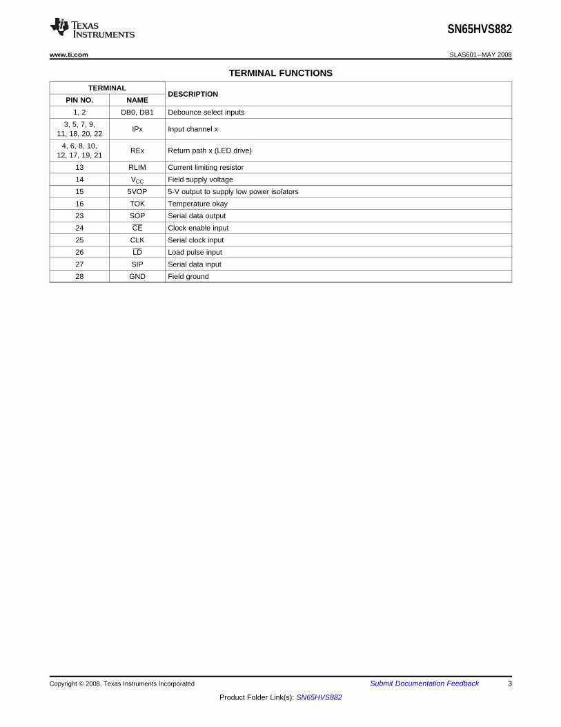
TERMINAL FUNCTIONSTERMINAL
DESCRIPTIONPIN NO. NAME
1, 2 DB0, DB1 Debounce select inputs3, 5, 7, 9, IPx Input channel x11, 18, 20, 22
4, 6, 8, 10, REx Return path x (LED drive)12, 17, 19, 2113 RLIM Current limiting resistor14 VCC Field supply voltage15 5VOP 5-V output to supply low power isolators16 TOK Temperature okay23 SOP Serial data output24 CE Clock enable input25 CLK Serial clock input26 LD Load pulse input27 SIP Serial data input28 GND Field ground
Copyright © 2008, Texas Instruments Incorporated Submit Documentation Feedback 3
Product Folder Link(s): SN65HVS882
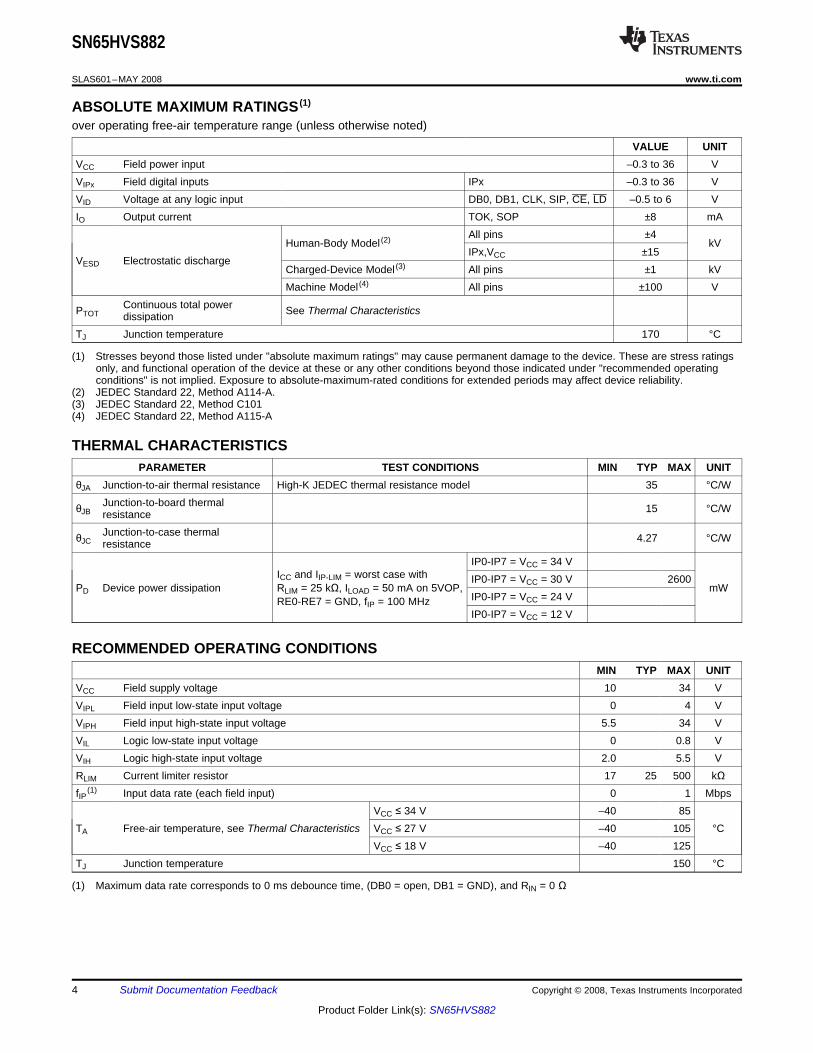
ABSOLUTE MAXIMUM RATINGS (1)
THERMAL CHARACTERISTICS
RECOMMENDED OPERATING CONDITIONS
SN65HVS882
SLAS601–MAY 2008 ........................................................................................................................................................................................................ www.ti.com
over operating free-air temperature range (unless otherwise noted)
VALUE UNITVCC Field power input –0.3 to 36 VVIPx Field digital inputs IPx –0.3 to 36 VVID Voltage at any logic input DB0, DB1, CLK, SIP, CE, LD –0.5 to 6 VIO Output current TOK, SOP ±8 mA
All pins ±4Human-Body Model (2) kV
IPx,VCC ±15VESD Electrostatic discharge
Charged-Device Model (3) All pins ±1 kVMachine Model (4) All pins ±100 V
Continuous total powerPTOT See Thermal CharacteristicsdissipationTJ Junction temperature 170 °C
(1) Stresses beyond those listed under "absolute maximum ratings" may cause permanent damage to the device. These are stress ratingsonly, and functional operation of the device at these or any other conditions beyond those indicated under "recommended operatingconditions" is not implied. Exposure to absolute-maximum-rated conditions for extended periods may affect device reliability.
(2) JEDEC Standard 22, Method A114-A.(3) JEDEC Standard 22, Method C101(4) JEDEC Standard 22, Method A115-A
PARAMETER TEST CONDITIONS MIN TYP MAX UNITθJA Junction-to-air thermal resistance High-K JEDEC thermal resistance model 35 °C/W
Junction-to-board thermalθJB 15 °C/WresistanceJunction-to-case thermalθJC 4.27 °C/Wresistance
IP0-IP7 = VCC = 34 VICC and IIP-LIM = worst case with IP0-IP7 = VCC = 30 V 2600
PD Device power dissipation RLIM = 25 kΩ, ILOAD = 50 mA on 5VOP, mWIP0-IP7 = VCC = 24 VRE0-RE7 = GND, fIP = 100 MHzIP0-IP7 = VCC = 12 V
MIN TYP MAX UNITVCC Field supply voltage 10 34 VVIPL Field input low-state input voltage 0 4 VVIPH Field input high-state input voltage 5.5 34 VVIL Logic low-state input voltage 0 0.8 VVIH Logic high-state input voltage 2.0 5.5 VRLIM Current limiter resistor 17 25 500 kΩfIP(1) Input data rate (each field input) 0 1 Mbps
VCC ≤ 34 V –40 85TA Free-air temperature, see Thermal Characteristics VCC ≤ 27 V –40 105 °C
VCC ≤ 18 V –40 125TJ Junction temperature 150 °C
(1) Maximum data rate corresponds to 0 ms debounce time, (DB0 = open, DB1 = GND), and RIN = 0 Ω
4 Submit Documentation Feedback Copyright © 2008, Texas Instruments Incorporated
Product Folder Link(s): SN65HVS882
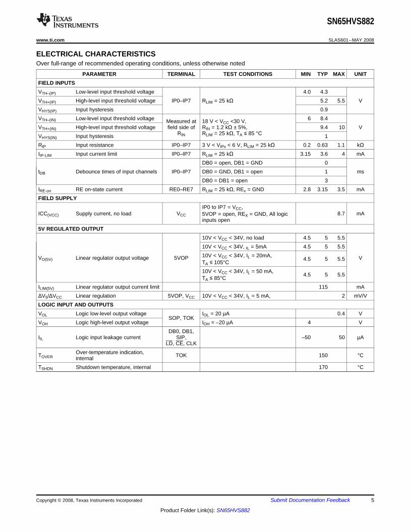
ELECTRICAL CHARACTERISTICS
SN65HVS882
www.ti.com ........................................................................................................................................................................................................ SLAS601–MAY 2008
Over full-range of recommended operating conditions, unless otherwise noted
PARAMETER TERMINAL TEST CONDITIONS MIN TYP MAX UNITFIELD INPUTSVTH–(IP) Low-level input threshold voltage 4.0 4.3VTH+(IP) High-level input threshold voltage IP0–IP7 RLIM = 25 kΩ 5.2 5.5 VVHYS(IP) Input hysteresis 0.9VTH–(IN) Low-level input threshold voltage 6 8.4Measured at 18 V < VCC <30 V,VTH+(IN) High-level input threshold voltage field side of RIN = 1.2 kΩ ± 5%, 9.4 10 V
RIN RLIM = 25 kΩ, TA ≤ 85 °CVHYS(IN) Input hysteresis 1RIP Input resistance IP0–IP7 3 V < VIPx < 6 V, RLIM = 25 kΩ 0.2 0.63 1.1 kΩIIP-LIM Input current limit IP0–IP7 RLIM = 25 kΩ 3.15 3.6 4 mA
DB0 = open, DB1 = GND 0tDB Debounce times of input channels IP0–IP7 DB0 = GND, DB1 = open 1 ms
DB0 = DB1 = open 3IRE-on RE on-state current RE0–RE7 RLIM = 25 kΩ, REx = GND 2.8 3.15 3.5 mAFIELD SUPPLY
IP0 to IP7 = VCC,ICC(VCC) Supply current, no load VCC 8.7 mA5VOP = open, REX = GND, All logic
inputs open5V REGULATED OUTPUT
10V < VCC < 34V, no load 4.5 5 5.510V < VCC < 34V, IL = 5mA 4.5 5 5.510V < VCC < 34V, IL = 20mA,VO(5V) Linear regulator output voltage 5VOP V4.5 5 5.5TA ≤ 105°C10V < VCC < 34V, IL = 50 mA, 4.5 5 5.5TA ≤ 85°C
ILIM(5V) Linear regulator output current limit 115 mAΔV5/ΔVCC Linear regulation 5VOP, VCC 10V < VCC < 34V, IL = 5 mA, 2 mV/VLOGIC INPUT AND OUTPUTSVOL Logic low-level output voltage IOL = 20 µA 0.4 V
SOP, TOKVOH Logic high-level output voltage IOH = –20 µA 4 V
DB0, DB1,IIL Logic input leakage current SIP, –50 50 µA
LD, CE, CLKOver-temperature indication,TOVER TOK 150 °Cinternal
TSHDN Shutdown temperature, internal 170 °C
Copyright © 2008, Texas Instruments Incorporated Submit Documentation Feedback 5
Product Folder Link(s): SN65HVS882

TIMING REQUIREMENTS
SWITCHING CHARACTERISTICS
SN65HVS882
SLAS601–MAY 2008 ........................................................................................................................................................................................................ www.ti.com
over operating free-air temperature range (unless otherwise noted)
PARAMETER MIN TYP MAX UNITtW1 CLK pulse duration See Figure 5 4 nstW2 LD pulse duration See Figure 3 6 nstSU1 SIP to CLK setup time See Figure 6 4 nstH1 SIP to CLK hold time See Figure 6 2 nstSU2 Falling edge to rising edge (CE to CLK) setup time See Figure 7 4 nstREC LD to CLK recovery time See Figure 4 2 nsfCLK Clock pulse frequency See Figure 5 DC 100 MHz
over operating free-air temperature range (unless otherwise noted)
PARAMETER TEST CONDITIONS MIN TYP MAX UNITtPLH1, tPHL1 CLK to SOP CL = 15 pF, see Figure 5 10 nstPLH2, tPHL2 LD to SOP CL = 15 pF, see Figure 3 14 nstr, tf Rise and fall times CL = 15 pF, see Figure 5 5 ns
6 Submit Documentation Feedback Copyright © 2008, Texas Instruments Incorporated
Product Folder Link(s): SN65HVS882
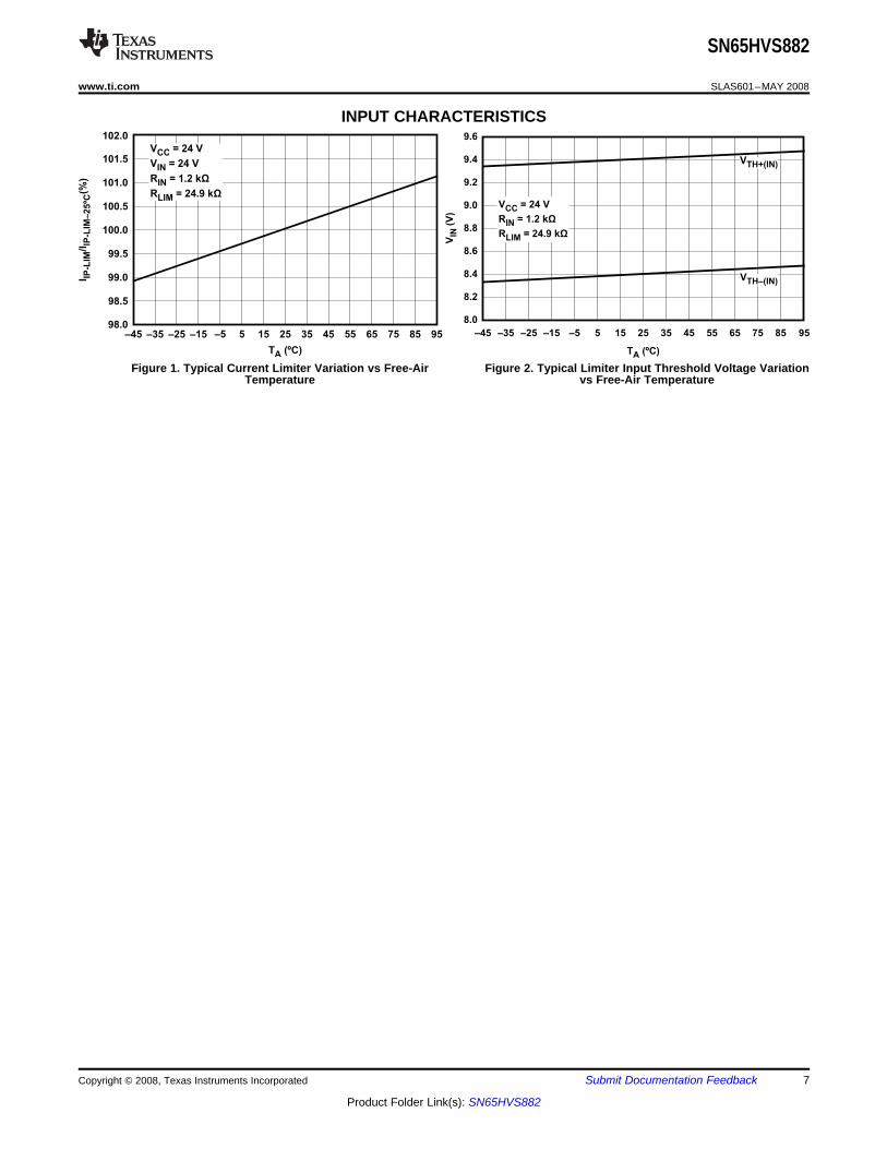
INPUT CHARACTERISTICS
T (ºC)A
I/
(%)
IP-L
IMI I
P-L
IM–2
5ºC
102.0
101.5
101.0
100.5
100.0
99.5
99.0
98.5
98.0
–45 –35 –25 –15 –5 5 15 25 35 45 55 65 75 85 95
V = 24 V
V
CC
IN
IN
LIM
= 24 V
R = 1.2 k
R = 24.9 k
Ω
Ω
T (ºC)A
V(V
)IN
9.6
9.4
9.2
9.0
8.8
8.6
8.4
8.2
8.0
–45 –35 –25 –15 –5 5 15 25 35 45 55 65 75 85 95
VTH+(IN)
VTH–(IN)
V = 24 VCC
R = 1.2 k
R = 24.9 k
IN
LIM
Ω
Ω
SN65HVS882
www.ti.com ........................................................................................................................................................................................................ SLAS601–MAY 2008
Figure 1. Typical Current Limiter Variation vs Free-Air Figure 2. Typical Limiter Input Threshold Voltage VariationTemperature vs Free-Air Temperature
Copyright © 2008, Texas Instruments Incorporated Submit Documentation Feedback 7
Product Folder Link(s): SN65HVS882
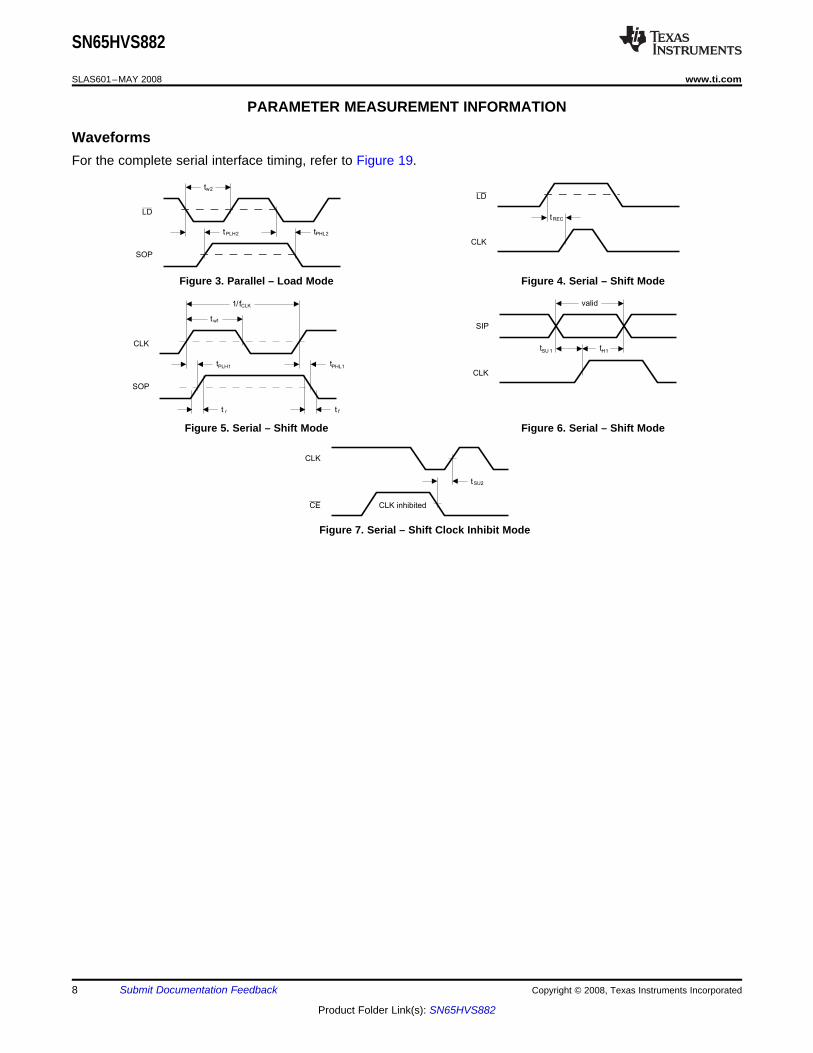
PARAMETER MEASUREMENT INFORMATION
Waveforms
CLK
tREC
LDtw2
tPLH2 tPHL2
LD
SOP
CLK
valid
tSU 1 tH1
SIP
CLK
tPLH1 tPHL1
t ft r
tw1
1/fCLK
SOP
CLK inhibited
tSU2
CLK
CE
SN65HVS882
SLAS601–MAY 2008 ........................................................................................................................................................................................................ www.ti.com
For the complete serial interface timing, refer to Figure 19.
Figure 3. Parallel – Load Mode Figure 4. Serial – Shift Mode
Figure 5. Serial – Shift Mode Figure 6. Serial – Shift Mode
Figure 7. Serial – Shift Clock Inhibit Mode
8 Submit Documentation Feedback Copyright © 2008, Texas Instruments Incorporated
Product Folder Link(s): SN65HVS882
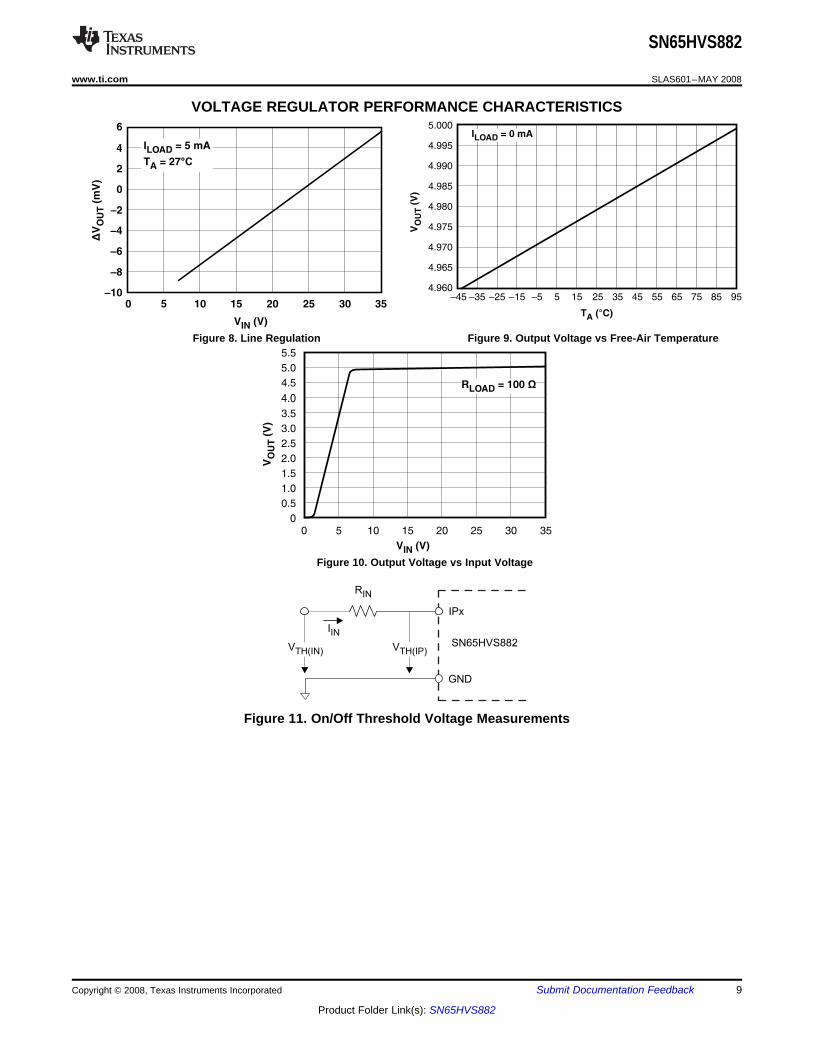
VOLTAGE REGULATOR PERFORMANCE CHARACTERISTICS
T (°C)A
V(V
)O
UT
5.000
4.995
4.990
4.985
4.980
4.975
4.970
4.965
4.960
–45 –35 –25 –15 –5 5 15 25 35 45 55 65 75 85 95
I = 0 mALOAD
V (V)IN
ΔV
(mV
)O
UT
6
4
2
0
–2
–4
–6
–8
–100 5 10 15 20 25 30 35
I = 5 mA
TLOAD
A = 27°C
V (V)IN
V(V
)O
UT
0 5 10 15 20 25 30 35
5.5
4.5
3.5
2.5
1.5
0.5
5.0
4.0
3.0
2.0
1.0
0
R = 100LOAD Ω
RIN
IPx
GND
SN65HVS882
IIN
VTH(IN) VTH(IP)
SN65HVS882
www.ti.com ........................................................................................................................................................................................................ SLAS601–MAY 2008
Figure 8. Line Regulation Figure 9. Output Voltage vs Free-Air Temperature
Figure 10. Output Voltage vs Input Voltage
Figure 11. On/Off Threshold Voltage Measurements
Copyright © 2008, Texas Instruments Incorporated Submit Documentation Feedback 9
Product Folder Link(s): SN65HVS882
DEVICE INFORMATION
Digital Inputs
Limiter
I = IINmax LIM
5 V
ILIM
IIN
IPx
RLIM
I Mirror
n = 72
LIM
IREF
V-REF
R =LIM
90
ILIM
90
2.5 mA
= 36 kΩ=
Debounce Filter
SN65HVS882
SLAS601–MAY 2008 ........................................................................................................................................................................................................ www.ti.com
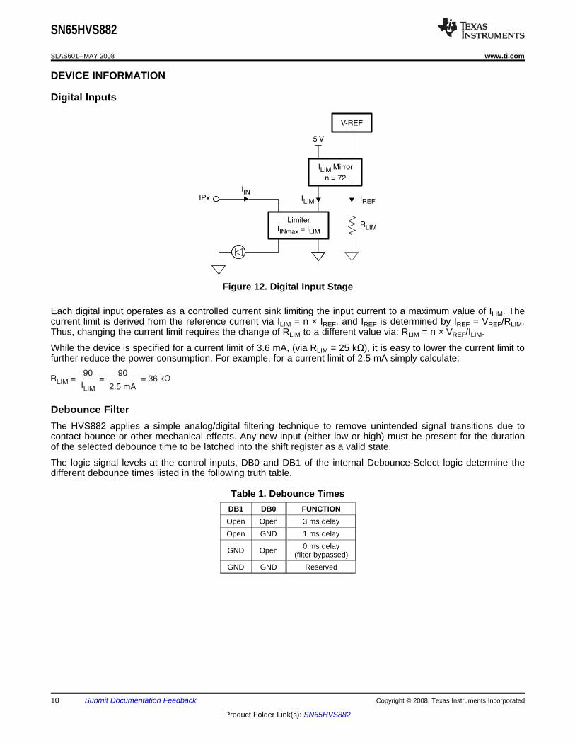
Figure 12. Digital Input Stage
Each digital input operates as a controlled current sink limiting the input current to a maximum value of ILIM. Thecurrent limit is derived from the reference current via ILIM = n × IREF, and IREF is determined by IREF = VREF/RLIM.Thus, changing the current limit requires the change of RLIM to a different value via: RLIM = n × VREF/ILIM.
While the device is specified for a current limit of 3.6 mA, (via RLIM = 25 kΩ), it is easy to lower the current limit tofurther reduce the power consumption. For example, for a current limit of 2.5 mA simply calculate:
The HVS882 applies a simple analog/digital filtering technique to remove unintended signal transitions due tocontact bounce or other mechanical effects. Any new input (either low or high) must be present for the durationof the selected debounce time to be latched into the shift register as a valid state.
The logic signal levels at the control inputs, DB0 and DB1 of the internal Debounce-Select logic determine thedifferent debounce times listed in the following truth table.
Table 1. Debounce TimesDB1 DB0 FUNCTIONOpen Open 3 ms delayOpen GND 1 ms delay
0 ms delayGND Open (filter bypassed)GND GND Reserved
10 Submit Documentation Feedback Copyright © 2008, Texas Instruments Incorporated
Product Folder Link(s): SN65HVS882
REF
RLIM
IPx
REx
GND
5 V
Shift Register
CP
D Q
SR
SOP
SIP
LD
PIP 1 PIP 2 PIP 3 PIP 4 PIP 5 PIP 6 PIP 7PIP 0
CLK
CE
Logic CP
D Q
SR
CP
D Q
SR
CP
D Q
SR
CP
D Q
SR
CP
D Q
SR
CP
D Q
SR
CP
D Q
SR
SN65HVS882
www.ti.com ........................................................................................................................................................................................................ SLAS601–MAY 2008
Figure 13. Equivalent Input Diagram
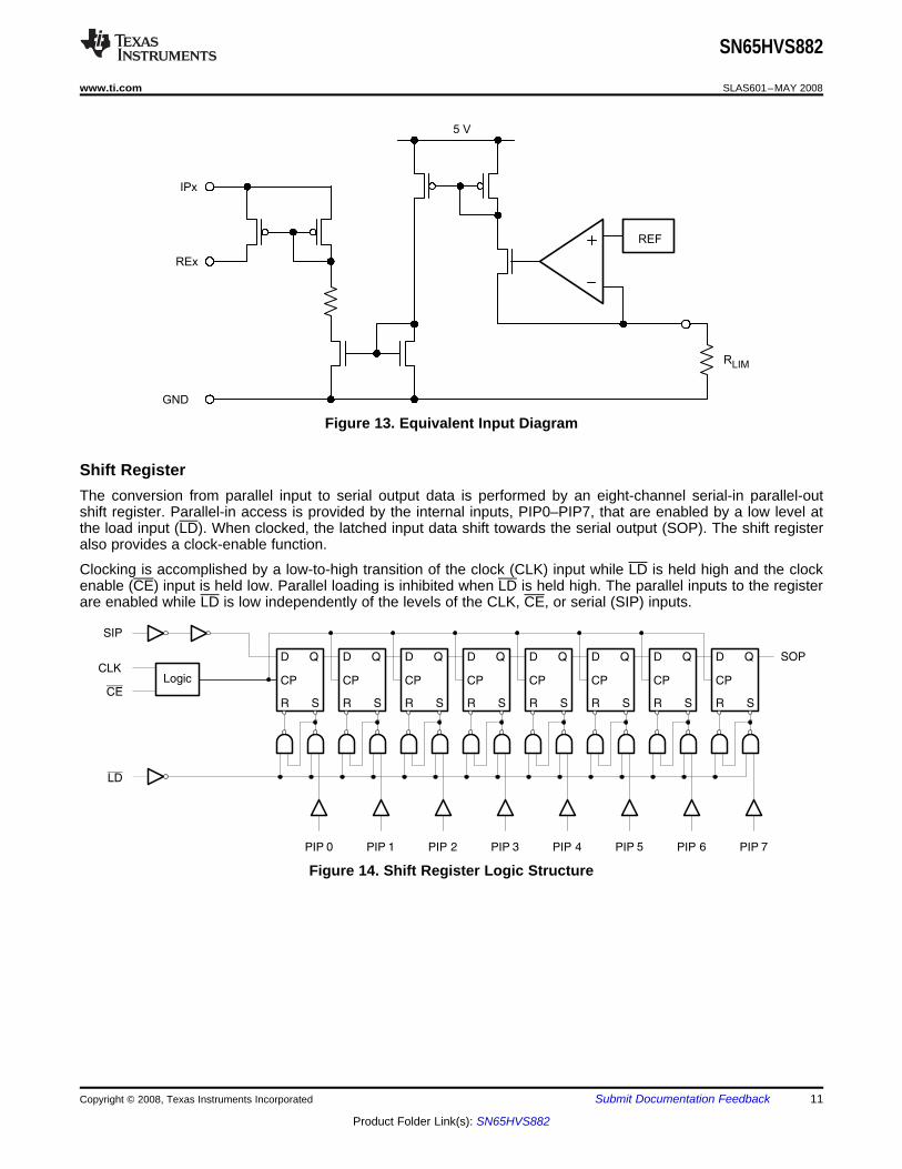
The conversion from parallel input to serial output data is performed by an eight-channel serial-in parallel-outshift register. Parallel-in access is provided by the internal inputs, PIP0–PIP7, that are enabled by a low level atthe load input (LD). When clocked, the latched input data shift towards the serial output (SOP). The shift registeralso provides a clock-enable function.
Clocking is accomplished by a low-to-high transition of the clock (CLK) input while LD is held high and the clockenable (CE) input is held low. Parallel loading is inhibited when LD is held high. The parallel inputs to the registerare enabled while LD is low independently of the levels of the CLK, CE, or serial (SIP) inputs.
Figure 14. Shift Register Logic Structure
Copyright © 2008, Texas Instruments Incorporated Submit Documentation Feedback 11
Product Folder Link(s): SN65HVS882

Voltage Regulator
>I
C
L-MIN
L
1 mA
1 µF
Temperature Sensor
SN65HVS882
SLAS601–MAY 2008 ........................................................................................................................................................................................................ www.ti.com
Table 2. Function TableINPUTS
FUNCTIONLD CLK CEL X X Parallel loadH X H No changeH ↑ L Shift (1)
(1) Shift = content of each internal register shifts towards serial outputs.Data at SIP is shifted into first register.
The on-chip linear voltage regulator provides a 5-V supply to the internal and external circuitry, such as digitalisolators, with an output drive capability of 50 mA and a typical current limit of 115 mA. The regulator acceptsinput voltages from 30 V down to 10 V. Because the regulator output is intended to supply external digital isolatorcircuits proper output voltage decoupling is required. For best results connect a 1-µF and a 0.1-µF ceramiccapacitor as close as possible to the 5VOP output. For longer traces between the SN65HVS882 and isolators ofthe ISO72xx family use additional 0.1-µF and 10-pF capacitors next to the isolator supply pins. Make sure,however, that the total load capacitance does not exceed 4.7 µF.
For good stability the voltage regulator requires a minimum load current, IL-MIN. Ensure that under any operatingcondition the ratio of the minimum load current in mA to the total load capacitance in µF is larger than 1:
An on-chip temperature sensor monitors the device temperature and signals a fault condition if the internaltemperature reaches 150°C. If the internal temperature exceeds this trip point, the TOK output switches to anactive low state. If the internal temperature continues to rise, passing a second trip point at 170°C, all deviceoutputs are put in a high-impedance state.
A special condition occurs, however, when the chip temperature exceeds the second temperature trip point dueto an output short. Then the output buffer becomes three-state, thus separating the buffer from the externalcircuitry. An internal 100-kΩ pull-down resistor, connecting the TOK pin to ground, is used as a cooling downresistor, which continues to provide a logic low level to the external circuitry.
12 Submit Documentation Feedback Copyright © 2008, Texas Instruments Incorporated
Product Folder Link(s): SN65HVS882

APPLICATION INFORMATION
System-Level EMC
VCC
IP0–IP7
GND
GND
D2
DS D1
R1
RIN
C1
CIN
VSUP = 24 V
CS
CS
0 V
IPx
0 V
FE
FE
SN65HVS882
D2
DS
D1
R1
RIN
C1
CIN
CS
Super rectifier: BYM10-1000 orGeneral purpose rectifier: 1N4007
39-V transient voltage suppressor, SM15T39CA
33–36-V fast Zener diode, ZSMB36
56- , 1/3-W MELF resistorΩ
1.2-kΩ, 1/4-W MELF resistor
10- F, 60-V ceramic capacitorμ
22-nF, 60-V ceramic capacitor
4.7-nF, 2-kV polypropylene capacitor
Input Channel Switching for IEC61131-2 PLC Applications
30
25
20
15
10
5
0
–3
5 10 15
30
25
20
15
10
5
0-–3
5 10 15
I (mA)IN
V(V
)IN
V(V
)IN
V(V
)IN
I (mA)INI (mA)IN
30
25
20
15
10
5
0–3
5 10 1520 25 30
Type 1 Type 2 Type 3
OFF
ON
OFFOFF
ONON
0
00
SN65HVS882
www.ti.com ........................................................................................................................................................................................................ SLAS601–MAY 2008
The SN65HVS882 is designed to operate reliably in harsh industrial environments. At a system level, the deviceis tested according to several international electromagnetic compatibility (EMC) standards. In addition to thedevice internal ESD structures, external protection circuitry, as shown in Figure 15, can be used to absorb asmuch energy from burst- and surge-transients as possible.
Figure 15. Typical EMC Protection Circuitry for Supply and Signal Inputs
The input stage of the SN65HVS882 is designed so that with a 24-V supply on VCC and an input resistor RIN =1.2 kΩ, the trip point for signaling an ON-condition is at 9.4 V at 3.6 mA. This trip point satisfies the switchingrequirements of IEC61131-2 type-1 and type-3 switches.
Figure 16. Switching Characteristics for IEC1131-2 Type 1, 2, and 3 Proximity Switches
For a type-2 switch application two inputs are connected in parallel. The current limiters then add to a totalmaximum current of 7.2 mA. While the return-path (RE-pin), of one input might be used to drive an indicatorLED, the RE-pin of the other input channel should be connected to ground (GND).
Paralleling input channels reduces the number of available input channels from an octal Type 1 or Type 3 inputto a quad Type 2 input device. Note, that in this configuration output data of an input channel is represented bytwo shift register bits.
Copyright © 2008, Texas Instruments Incorporated Submit Documentation Feedback 13
Product Folder Link(s): SN65HVS882
RIN
RIN R
IN
CIN
CIN
CIN
CIN
RIN
RE0 RE0
IP0 IP0
RE1 RE1
IP1 IP1
Digital Interface Timing
IP0
IP7
SN65HVS882
ISO7241
SE
RIA
LIZ
ER
HOSTCONTROLLERSIP
LD
CE
CLK
SOP
OUTA
OUTB
OUTC
IND
INA
INB
INC
OUTD
LOAD
STE
SCLK
SOMI
VREG5 VVCC
SN65HVS882
SLAS601–MAY 2008 ........................................................................................................................................................................................................ www.ti.com
Figure 17. Paralleling Two Type 1 or Type 3 Inputs Into One Type 2 Input
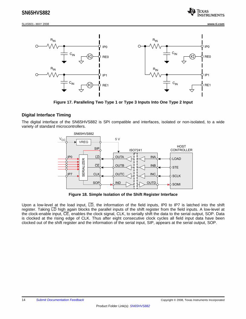
The digital interface of the SN65HVS882 is SPI compatible and interfaces, isolated or non-isolated, to a widevariety of standard microcontrollers.
Figure 18. Simple Isolation of the Shift Register Interface
Upon a low-level at the load input, LD, the information of the field inputs, IP0 to IP7 is latched into the shiftregister. Taking LD high again blocks the parallel inputs of the shift register from the field inputs. A low-level atthe clock-enable input, CE, enables the clock signal, CLK, to serially shift the data to the serial output, SOP. Datais clocked at the rising edge of CLK. Thus after eight consecutive clock cycles all field input data have beenclocked out of the shift register and the information of the serial input, SIP, appears at the serial output, SOP.
14 Submit Documentation Feedback Copyright © 2008, Texas Instruments Incorporated
Product Folder Link(s): SN65HVS882

IP6 IP5 IP4 IP3 IP2 IP1 IP0 SIPIP7don’t care
CLK
CE
LD
SIP
PIP0–PIP6
PIP7
SOP
inhibit
high
Serial shift
Cascading for High Channel Count Input Modules
4 SN65HVS882X
OUTA
OUTB
OUTC
IND
INA
INB
INC
OUTD
ISO7241HOST
CONTROLLER
LOAD
STE
SCLK
SOMI
SERIALIZER SERIALIZER SERIALIZER SERIALIZER
SIP LD
CE
CL
K
SO
P
SIP LD
CE
CL
K
SO
P
SIP LD
CE
CL
K
SO
P
IP0
IP7
IP0
IP7
IP0
IP7
IP0
IP7
SIP LD
CE
CL
K
SO
P
SN65HVS882
www.ti.com ........................................................................................................................................................................................................ SLAS601–MAY 2008
Figure 19. Interface Timing for Parallel-Load and Serial-Shift Operation of the Shift Register
Designing high-channel count modules requires cascading multiple SN65HVS882 devices. Simply connect theserial output (SOP) of a leading device with the serial input (SIP) of a following device without changing theprocessor interface.
Figure 20. Cascading Four SN65HVS882 for a 32-Channel Input Module
Copyright © 2008, Texas Instruments Incorporated Submit Documentation Feedback 15
Product Folder Link(s): SN65HVS882
Typical Digital Input Module Application
IsolatedDC/DC
SIP
LD
CE
CLK
SOP
5VOP
TOK
DB0
DB1
VCC
IP0
RE0
IP7
RE7
RLIM
GND
SN65HVS882
S0
S7
ISO7242
GND2
EN2
VCC2
INA
GND1
EN1
VCC1
OUTA
OUTB
INC
IND
INB
OUTC
OUTD
HOSTCONTROLLER
LOAD
SCLK
INT
SOMI
DGND
VCC
24V2
24V1
0 V
FE
(Logic)
(Sensors)
PowerSupply
22 nF
22 nF
Sre
wTe
rmin
als
1N4007
Z2SMB36
4.7 nF2 kV
4.7 nF2 kV4.7 nF
2 kV
SM15T39CA
SM15T39A
1.2 kMELF
Ω
1.2 kMELF
Ω
56 MELFΩ
24.9 kΩ
10 F60 V
m
0.1 Fm
5V-ISO
0V-ISO
24 V
GND2
5 V
GND1
1 Fm
SN65HVS882
SLAS601–MAY 2008 ........................................................................................................................................................................................................ www.ti.com
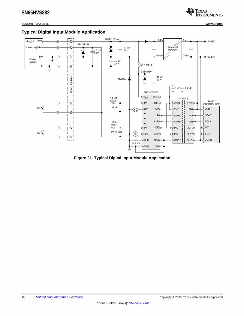
Figure 21. Typical Digital Input Module Application
16 Submit Documentation Feedback Copyright © 2008, Texas Instruments Incorporated
Product Folder Link(s): SN65HVS882
PACKAGE OPTION ADDENDUM
www.ti.com 24-Aug-2018
Addendum-Page 1
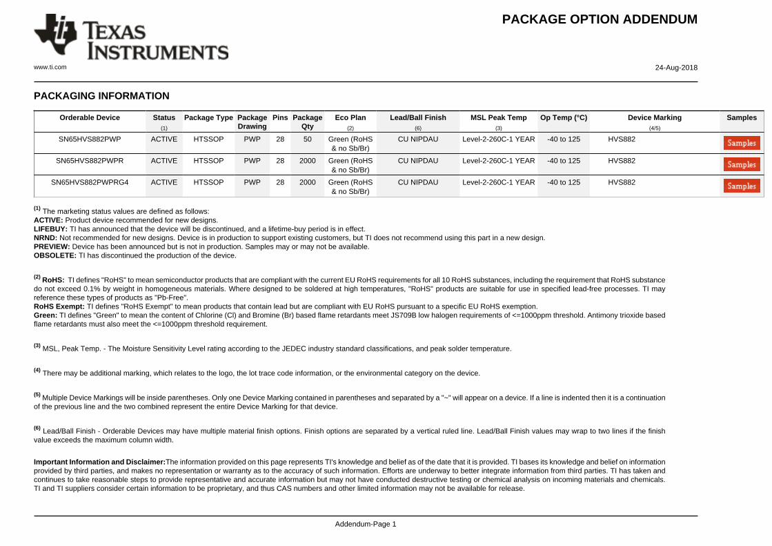
PACKAGING INFORMATION
Orderable Device Status(1)
Package Type PackageDrawing
Pins PackageQty
Eco Plan(2)
Lead/Ball Finish(6)
MSL Peak Temp(3)
Op Temp (°C) Device Marking(4/5)
Samples
SN65HVS882PWP ACTIVE HTSSOP PWP 28 50 Green (RoHS& no Sb/Br)
CU NIPDAU Level-2-260C-1 YEAR -40 to 125 HVS882
SN65HVS882PWPR ACTIVE HTSSOP PWP 28 2000 Green (RoHS& no Sb/Br)
CU NIPDAU Level-2-260C-1 YEAR -40 to 125 HVS882
SN65HVS882PWPRG4 ACTIVE HTSSOP PWP 28 2000 Green (RoHS& no Sb/Br)
CU NIPDAU Level-2-260C-1 YEAR -40 to 125 HVS882
(1) The marketing status values are defined as follows:ACTIVE: Product device recommended for new designs.LIFEBUY: TI has announced that the device will be discontinued, and a lifetime-buy period is in effect.NRND: Not recommended for new designs. Device is in production to support existing customers, but TI does not recommend using this part in a new design.PREVIEW: Device has been announced but is not in production. Samples may or may not be available.OBSOLETE: TI has discontinued the production of the device.
(2) RoHS: TI defines "RoHS" to mean semiconductor products that are compliant with the current EU RoHS requirements for all 10 RoHS substances, including the requirement that RoHS substancedo not exceed 0.1% by weight in homogeneous materials. Where designed to be soldered at high temperatures, "RoHS" products are suitable for use in specified lead-free processes. TI mayreference these types of products as "Pb-Free".RoHS Exempt: TI defines "RoHS Exempt" to mean products that contain lead but are compliant with EU RoHS pursuant to a specific EU RoHS exemption.Green: TI defines "Green" to mean the content of Chlorine (Cl) and Bromine (Br) based flame retardants meet JS709B low halogen requirements of <=1000ppm threshold. Antimony trioxide basedflame retardants must also meet the <=1000ppm threshold requirement.
(3) MSL, Peak Temp. - The Moisture Sensitivity Level rating according to the JEDEC industry standard classifications, and peak solder temperature.
(4) There may be additional marking, which relates to the logo, the lot trace code information, or the environmental category on the device.
(5) Multiple Device Markings will be inside parentheses. Only one Device Marking contained in parentheses and separated by a "~" will appear on a device. If a line is indented then it is a continuationof the previous line and the two combined represent the entire Device Marking for that device.
(6) Lead/Ball Finish - Orderable Devices may have multiple material finish options. Finish options are separated by a vertical ruled line. Lead/Ball Finish values may wrap to two lines if the finishvalue exceeds the maximum column width.
Important Information and Disclaimer:The information provided on this page represents TI's knowledge and belief as of the date that it is provided. TI bases its knowledge and belief on informationprovided by third parties, and makes no representation or warranty as to the accuracy of such information. Efforts are underway to better integrate information from third parties. TI has taken andcontinues to take reasonable steps to provide representative and accurate information but may not have conducted destructive testing or chemical analysis on incoming materials and chemicals.TI and TI suppliers consider certain information to be proprietary, and thus CAS numbers and other limited information may not be available for release.
PACKAGE OPTION ADDENDUM
www.ti.com 24-Aug-2018
Addendum-Page 2
In no event shall TI's liability arising out of such information exceed the total purchase price of the TI part(s) at issue in this document sold by TI to Customer on an annual basis.

TAPE AND REEL INFORMATION
*All dimensions are nominal
Device PackageType
PackageDrawing
Pins SPQ ReelDiameter
(mm)
ReelWidth
W1 (mm)
A0(mm)
B0(mm)
K0(mm)
P1(mm)
W(mm)
Pin1Quadrant
SN65HVS882PWPR HTSSOP PWP 28 2000 330.0 16.4 6.9 10.2 1.8 12.0 16.0 Q1
PACKAGE MATERIALS INFORMATION
www.ti.com 26-Jan-2013
Pack Materials-Page 1
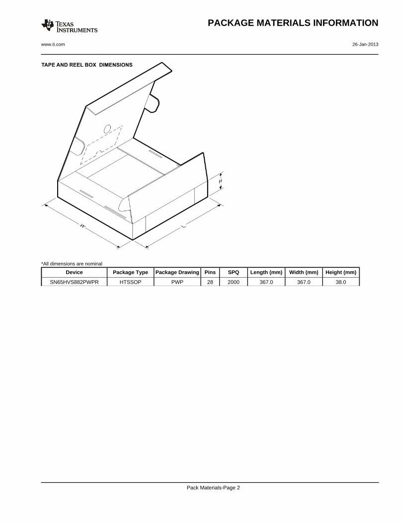
*All dimensions are nominal
Device Package Type Package Drawing Pins SPQ Length (mm) Width (mm) Height (mm)
SN65HVS882PWPR HTSSOP PWP 28 2000 367.0 367.0 38.0
PACKAGE MATERIALS INFORMATION
www.ti.com 26-Jan-2013
Pack Materials-Page 2
IMPORTANT NOTICE
Texas Instruments Incorporated (TI) reserves the right to make corrections, enhancements, improvements and other changes to itssemiconductor products and services per JESD46, latest issue, and to discontinue any product or service per JESD48, latest issue. Buyersshould obtain the latest relevant information before placing orders and should verify that such information is current and complete.TI’s published terms of sale for semiconductor products (http://www.ti.com/sc/docs/stdterms.htm) apply to the sale of packaged integratedcircuit products that TI has qualified and released to market. Additional terms may apply to the use or sale of other types of TI products andservices.Reproduction of significant portions of TI information in TI data sheets is permissible only if reproduction is without alteration and isaccompanied by all associated warranties, conditions, limitations, and notices. TI is not responsible or liable for such reproduceddocumentation. Information of third parties may be subject to additional restrictions. Resale of TI products or services with statementsdifferent from or beyond the parameters stated by TI for that product or service voids all express and any implied warranties for theassociated TI product or service and is an unfair and deceptive business practice. TI is not responsible or liable for any such statements.Buyers and others who are developing systems that incorporate TI products (collectively, “Designers”) understand and agree that Designersremain responsible for using their independent analysis, evaluation and judgment in designing their applications and that Designers havefull and exclusive responsibility to assure the safety of Designers' applications and compliance of their applications (and of all TI productsused in or for Designers’ applications) with all applicable regulations, laws and other applicable requirements. Designer represents that, withrespect to their applications, Designer has all the necessary expertise to create and implement safeguards that (1) anticipate dangerousconsequences of failures, (2) monitor failures and their consequences, and (3) lessen the likelihood of failures that might cause harm andtake appropriate actions. Designer agrees that prior to using or distributing any applications that include TI products, Designer willthoroughly test such applications and the functionality of such TI products as used in such applications.TI’s provision of technical, application or other design advice, quality characterization, reliability data or other services or information,including, but not limited to, reference designs and materials relating to evaluation modules, (collectively, “TI Resources”) are intended toassist designers who are developing applications that incorporate TI products; by downloading, accessing or using TI Resources in anyway, Designer (individually or, if Designer is acting on behalf of a company, Designer’s company) agrees to use any particular TI Resourcesolely for this purpose and subject to the terms of this Notice.TI’s provision of TI Resources does not expand or otherwise alter TI’s applicable published warranties or warranty disclaimers for TIproducts, and no additional obligations or liabilities arise from TI providing such TI Resources. TI reserves the right to make corrections,enhancements, improvements and other changes to its TI Resources. TI has not conducted any testing other than that specificallydescribed in the published documentation for a particular TI Resource.Designer is authorized to use, copy and modify any individual TI Resource only in connection with the development of applications thatinclude the TI product(s) identified in such TI Resource. NO OTHER LICENSE, EXPRESS OR IMPLIED, BY ESTOPPEL OR OTHERWISETO ANY OTHER TI INTELLECTUAL PROPERTY RIGHT, AND NO LICENSE TO ANY TECHNOLOGY OR INTELLECTUAL PROPERTYRIGHT OF TI OR ANY THIRD PARTY IS GRANTED HEREIN, including but not limited to any patent right, copyright, mask work right, orother intellectual property right relating to any combination, machine, or process in which TI products or services are used. Informationregarding or referencing third-party products or services does not constitute a license to use such products or services, or a warranty orendorsement thereof. Use of TI Resources may require a license from a third party under the patents or other intellectual property of thethird party, or a license from TI under the patents or other intellectual property of TI.TI RESOURCES ARE PROVIDED “AS IS” AND WITH ALL FAULTS. TI DISCLAIMS ALL OTHER WARRANTIES ORREPRESENTATIONS, EXPRESS OR IMPLIED, REGARDING RESOURCES OR USE THEREOF, INCLUDING BUT NOT LIMITED TOACCURACY OR COMPLETENESS, TITLE, ANY EPIDEMIC FAILURE WARRANTY AND ANY IMPLIED WARRANTIES OFMERCHANTABILITY, FITNESS FOR A PARTICULAR PURPOSE, AND NON-INFRINGEMENT OF ANY THIRD PARTY INTELLECTUALPROPERTY RIGHTS. TI SHALL NOT BE LIABLE FOR AND SHALL NOT DEFEND OR INDEMNIFY DESIGNER AGAINST ANY CLAIM,INCLUDING BUT NOT LIMITED TO ANY INFRINGEMENT CLAIM THAT RELATES TO OR IS BASED ON ANY COMBINATION OFPRODUCTS EVEN IF DESCRIBED IN TI RESOURCES OR OTHERWISE. IN NO EVENT SHALL TI BE LIABLE FOR ANY ACTUAL,DIRECT, SPECIAL, COLLATERAL, INDIRECT, PUNITIVE, INCIDENTAL, CONSEQUENTIAL OR EXEMPLARY DAMAGES INCONNECTION WITH OR ARISING OUT OF TI RESOURCES OR USE THEREOF, AND REGARDLESS OF WHETHER TI HAS BEENADVISED OF THE POSSIBILITY OF SUCH DAMAGES.Unless TI has explicitly designated an individual product as meeting the requirements of a particular industry standard (e.g., ISO/TS 16949and ISO 26262), TI is not responsible for any failure to meet such industry standard requirements.Where TI specifically promotes products as facilitating functional safety or as compliant with industry functional safety standards, suchproducts are intended to help enable customers to design and create their own applications that meet applicable functional safety standardsand requirements. Using products in an application does not by itself establish any safety features in the application. Designers mustensure compliance with safety-related requirements and standards applicable to their applications. Designer may not use any TI products inlife-critical medical equipment unless authorized officers of the parties have executed a special contract specifically governing such use.Life-critical medical equipment is medical equipment where failure of such equipment would cause serious bodily injury or death (e.g., lifesupport, pacemakers, defibrillators, heart pumps, neurostimulators, and implantables). Such equipment includes, without limitation, allmedical devices identified by the U.S. Food and Drug Administration as Class III devices and equivalent classifications outside the U.S.TI may expressly designate certain products as completing a particular qualification (e.g., Q100, Military Grade, or Enhanced Product).Designers agree that it has the necessary expertise to select the product with the appropriate qualification designation for their applicationsand that proper product selection is at Designers’ own risk. Designers are solely responsible for compliance with all legal and regulatoryrequirements in connection with such selection.Designer will fully indemnify TI and its representatives against any damages, costs, losses, and/or liabilities arising out of Designer’s non-compliance with the terms and provisions of this Notice.
Mailing Address: Texas Instruments, Post Office Box 655303, Dallas, Texas 75265Copyright © 2018, Texas Instruments Incorporated