Embed Size (px)
Citation preview
International Journal of Scientific & Engineering Research, Volume 4, Issue 5, May-2013 269 ISSN 2229-5518
IJSER © 2013 http://www.ijser.org
Single Electron Transistor: A Review Parikshit Sahatiya
Department of Physics and Nanotechnology, SRM University, Kattankulathur Campus Email: [email protected]
The goal of this paper is to review the physics of Single Electron Transistor (SET) and also the recent trends involve in fabrication of SET. The paper focuses on the application of SET in charge sensing, memories, logic families etc. Paper also briefs about the simulation of SET by TCAD, SIMPLORER, and SIMAN. SET are promising candidate for replacement of conventional CMOS and also following Moore Law. Even if this replacement does not happen, Single electronics will continue to play an important role by shedding light on fundamental size limit on new electronic devices. Moreover, research in this field has generated many novel ideas which may revolutionize Random-access-memories and Digital-data-storage technologies[1].
Index Terms: Single Electron Transistor, Tunneling, Coulomb Blockade, Electron beam Lithography, STM/AFM, TCAD, SIMPLORER, SIMAN, SET Memory.
IJSER
International Journal of Scientific & Engineering Research, Volume 4, Issue 5, May-2013 270 ISSN 2229-5518
IJSER © 2013 http://www.ijser.org
SINGLE ELECTRONICS IDEA
The idea of SET was demonstrated by Millikan at beginning of the century, but in solid state physics it was not implemented until the late 1980’s, despite some earlier background work. The main delay is manipulation of single electron and the fabrication needs to be very sophisticated which was not available at that time. The necessary nanofabrication techniques needed for the growth of Single Electronics have been developed in last two decades for the new field of solid state electronics: Single Electronics[1][2].
SINGLE ELECTRON TRANSISTOR PHYSICS
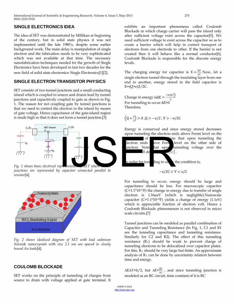
SET consists of two tunnel junctions and a small conducting island which is coupled to source and drains lead by tunnel junctions and capacitively coupled to gate as shown in Fig. 1. The reason for not coupling gate by tunnel junctions is that we need to control the electron in the island by means of gate voltage. Hence capacitance of the gate-island region is made high so that it does not form a tunnel junction.[3]
Fig. 1 shows basic electrical representation of SET where tunnel junctions are represented by capacitor connected parallel to resistor[4].
Fig. 2 shows idealized diagram of SET with lead cadmium Selenide nanocrystals with size 2.1 nm are spaced to closely bound Au leads[4].
COULOMB BLOCKADE
SET works on the principle of tunneling of charges from source to drain with voltage applied at gate terminal. It
exhibits an important phenomena called Coulomb Blockade in which charge carrier will pass the island only after sufficient voltage exist across the capacitor[5]. We need sufficient voltage to exist across the capacitor so as to create a barrier which will help in control transport of electrons from one electrode to other. If the barrier is not created then it will behave like a normal conductor[6]. Coulomb Blockade is responsible for the discrete energy levels.
The charging energy for capacitor is E = Q22C
. Now, let a single electron tunnel through the insulating layer from one end to another, energy stored in the field capacitor is E=(Q+e)2/2C.
Change in energy is∆E =−e(Q+e2)
C
For tunneling to occur ∆E>0 Therefore,
Q + e2 > 0 ,Q > −e/2 , V > −e/2C
Energy is conserved and since energy stored decreases upon tunneling the electron ends above Fermi level on the other side of junction. Note that upon tunneling the electron ends above Fermi level on the other side of junction. Note that upon tunneling voltage over the junction will decrease bye/c.
In order for tunneling to occur the condition is,
−e/2C < V < e/2
For tunneling to occur, energy should be large and capacitance should be less. For macroscopic capacitor (C=1.1*10-13F) the change in energy due to transfer of single electron is 1.16µeV (which is negligible).Nanoscale capacitor (C=1.1*10-19F) yields a change of energy (1.1eV) which is appreciable fraction of electron volt. Hence a Coulomb Blockade phenomenon is not observed in micro scale circuits.[7]
Tunnel junctions can be modeled as parallel combination of Capacitor and Tunneling Resistance (In Fig. 1, C1 and R1 are the tunneling capacitance and tunneling resistance. Similarly for C2 and R2). The effect of this tunneling resistance (RT) should be weak to prevent charge of tunneling electrons to be delocalized over capacitor plates. For this, RT should be very large but finite. An approximate analysis of RT can be done by uncertainty relation between time and energy.
∆E∆T>h/2, but ∆E=Q22C
, and since tunneling junction is modeled as an RC circuit, time constant of it is RC
IJSER
International Journal of Scientific & Engineering Research, Volume 4, Issue 5, May-2013 271 ISSN 2229-5518
IJSER © 2013 http://www.ijser.org
Therefore, substituting and solving for R we get the value of R=25.6KΩ [8].Hence the conditions for coulomb Blockade to occur is
1) The capacitance of the tunneling junction should be very small, in atto Farads.
2) The Resistance of tunneling junction should be greater than 25.6KΩ.
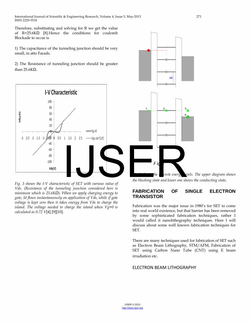
Fig. 3 shows the I-V characteristic of SET with various value of Vds. (Resistance of the tunneling junction considered here is minimum which is 25.6KΩ). When we apply charging energy to gate, Id flows instantaneously on application of Vds, while if gate voltage is kept zero then it takes energy from Vds to charge the island. The voltage needed to charge the island when Vg=0 is calculated as 0.72 V[4] [9][10].
F ig 4
Fig 4 shows the discrete energy levels. The upper diagram shows the blocking state and lower one shows the conducting state.
FABRICATION OF SINGLE ELECTRON TRANSISTOR
Fabrication was the major issue in 1980’s for SET to come into real world existence, but that barrier has been removed by some sophisticated fabrication techniques, rather I would called it nanolithography techniques. Here I will discuss about some well known fabrication techniques for SET.
There are many techniques used for fabrication of SET such as Electron Beam Lithography, STM/AFM, Fabrication of SET using Carbon Nano Tube (CNT) using E beam irradiation etc.
ELECTRON BEAM LITHOGRAPHY
IJSER
International Journal of Scientific & Engineering Research, Volume 4, Issue 5, May-2013 272 ISSN 2229-5518
IJSER © 2013 http://www.ijser.org
Fig 5
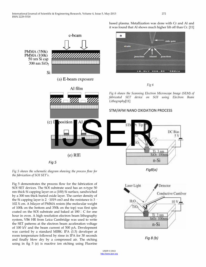
Fig 5 shows the schematic diagram showing the process flow for the fabrication of SOI SET’s.
Fig 5 demonstrates the process flow for the fabrication of SOI SET devices. The SOI substrate used has an n-type 50 nm thick Si capping layer on a (100) Si surface, sandwiched by a 300 nm thick buried oxide layer. The carrier density of the Si capping layer is 2 · 1019 cm3 and the resistance is 3 · 102 X cm. A bilayer of PMMA resists (the molecular weight of 100k on the bottom and 350k on the top) was first spin coated on the SOI substrate and baked at 180 o C for one hour in oven. A high resolution electron beam lithography system, VB6 HR from Leica Cambridge was used to write the SET patterns at the electron beam acceleration voltage of 100 kV and the beam current of 500 pA. Development was carried by a standard MIBK: IPA (1:3) developer at room temperature followed by rinse in IPA for 30 seconds and finally blow dry by a compressed air. The etching using in fig 5 (e) is reactive ion etching using Fluorine
based plasma. Metallization was done with Cr and Al and it was found that Al shows much higher lift off than Cr. [11]
Fig 6
Fig 6 shows the Scanning Electron Microscope Image (SEM) of fabricated SET device on SOI using Electron Beam Lithography[11]
STM/AFM NANO OXIDATION PROCESS
Fig8(a)
Fig 8 (b)
IJSER
International Journal of Scientific & Engineering Research, Volume 4, Issue 5, May-2013 273 ISSN 2229-5518
IJSER © 2013 http://www.ijser.org
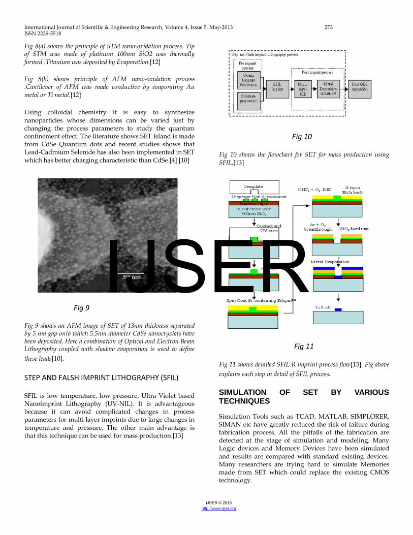
Fig 8(a) shows the principle of STM nano-oxidation process. Tip of STM was made of platinum 100nm SiO2 was thermally formed .Titanium was deposited by Evaporation.[12]
Fig 8(b) shows principle of AFM nano-oxidation process .Cantilever of AFM was made conductive by evaporating Au metal or Ti metal.[12]
Using colloidal chemistry it is easy to synthesize nanoparticles whose dimensions can be varied just by changing the process parameters to study the quantum confinement effect. The literature shows SET Island is made from CdSe Quantum dots and recent studies shows that Lead-Cadmium Selenide has also been implemented in SET which has better charging characteristic than CdSe.[4] [10]
Fig 9
Fig 9 shows an AFM image of SET of 13nm thickness separated by 5 nm gap onto which 5.5nm diameter CdSe nanocrystals have been deposited. Here a combination of Optical and Electron Beam Lithography coupled with shadow evaporation is used to define these leads[10].
STEP AND FALSH IMPRINT LITHOGRAPHY (SFIL)
SFIL is low temperature, low pressure, Ultra Violet based Nanoimprint Lithography (UV-NIL). It is advantageous because it can avoid complicated changes in process parameters for multi layer imprints due to large changes in temperature and pressure. The other main advantage is that this technique can be used for mass production.[13]
Fig 10
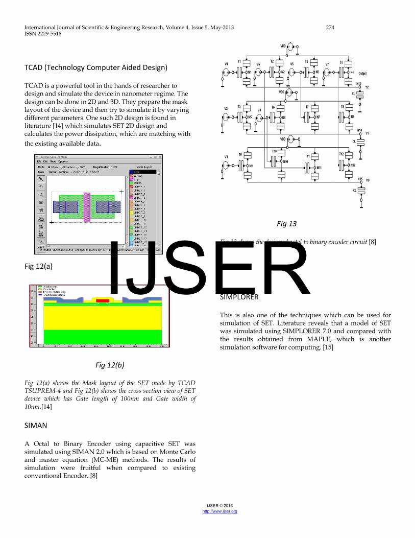
Fig 10 shows the flowchart for SET for mass production using SFIL.[13]
Fig 11
Fig 11 shows detailed SFIL-R imprint process flow[13]. Fig above explains each step in detail of SFIL process.
SIMULATION OF SET BY VARIOUS TECHNIQUES
Simulation Tools such as TCAD, MATLAB, SIMPLORER, SIMAN etc have greatly reduced the risk of failure during fabrication process. All the pitfalls of the fabrication are detected at the stage of simulation and modeling. Many Logic devices and Memory Devices have been simulated and results are compared with standard existing devices. Many researchers are trying hard to simulate Memories made from SET which could replace the existing CMOS technology.
IJSER
International Journal of Scientific & Engineering Research, Volume 4, Issue 5, May-2013 274 ISSN 2229-5518
IJSER © 2013 http://www.ijser.org
TCAD (Technology Computer Aided Design)
TCAD is a powerful tool in the hands of researcher to design and simulate the device in nanometer regime. The design can be done in 2D and 3D. They prepare the mask layout of the device and then try to simulate it by varying different parameters. One such 2D design is found in literature [14] which simulates SET 2D design and calculates the power dissipation, which are matching with the existing available data.
. Fig 12(a)
Fig 12(b)
Fig 12(a) shows the Mask layout of the SET made by TCAD TSUPREM-4 and Fig 12(b) shows the cross section view of SET device which has Gate length of 100nm and Gate width of 10nm.[14]
SIMAN
A Octal to Binary Encoder using capacitive SET was simulated using SIMAN 2.0 which is based on Monte Carlo and master equation (MC-ME) methods. The results of simulation were fruitful when compared to existing conventional Encoder. [8]
Fig 13
Fig 13 shows the designed octal to binary encoder circuit [8]
SIMPLORER
This is also one of the techniques which can be used for simulation of SET. Literature reveals that a model of SET was simulated using SIMPLORER 7.0 and compared with the results obtained from MAPLE, which is another simulation software for computing. [15]
IJSER
International Journal of Scientific & Engineering Research, Volume 4, Issue 5, May-2013 275 ISSN 2229-5518
IJSER © 2013 http://www.ijser.org
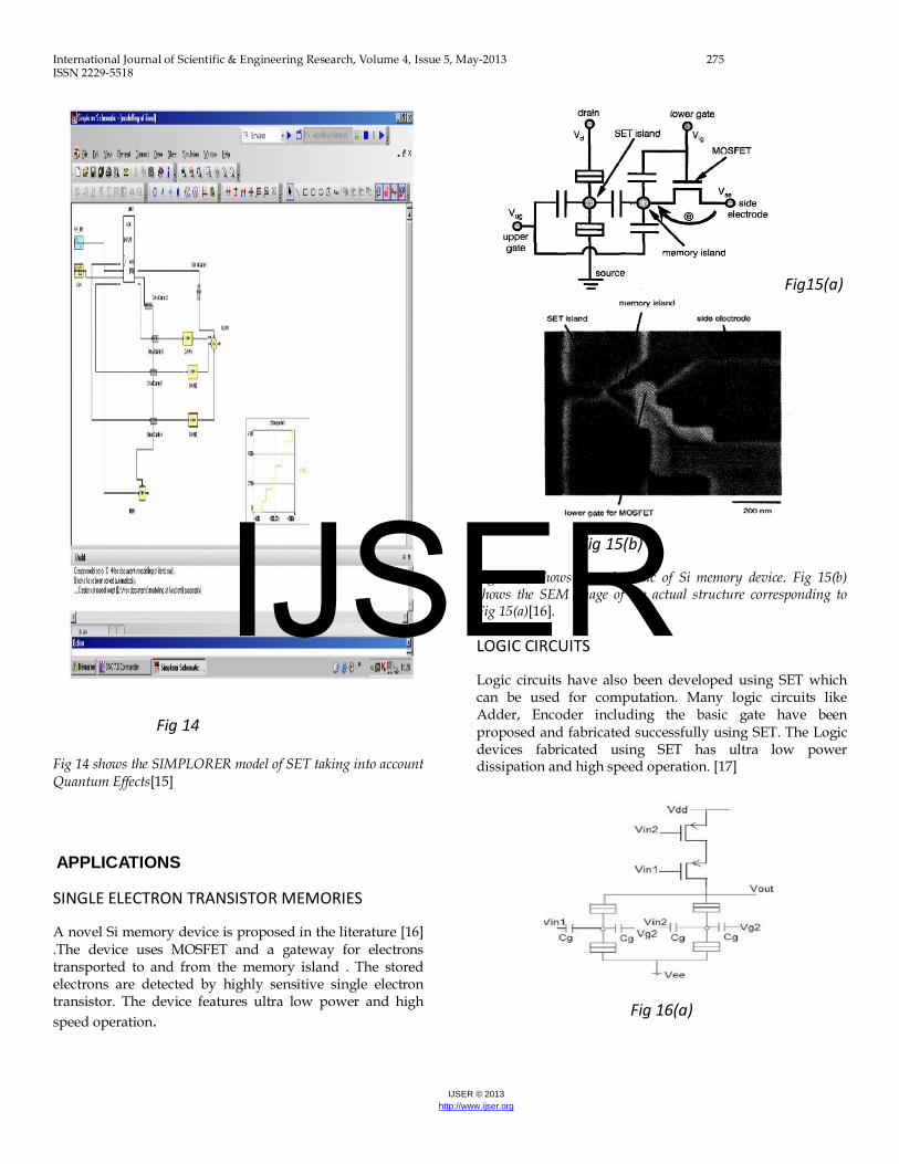
Fig 14
Fig 14 shows the SIMPLORER model of SET taking into account Quantum Effects[15]
APPLICATIONS
SINGLE ELECTRON TRANSISTOR MEMORIES
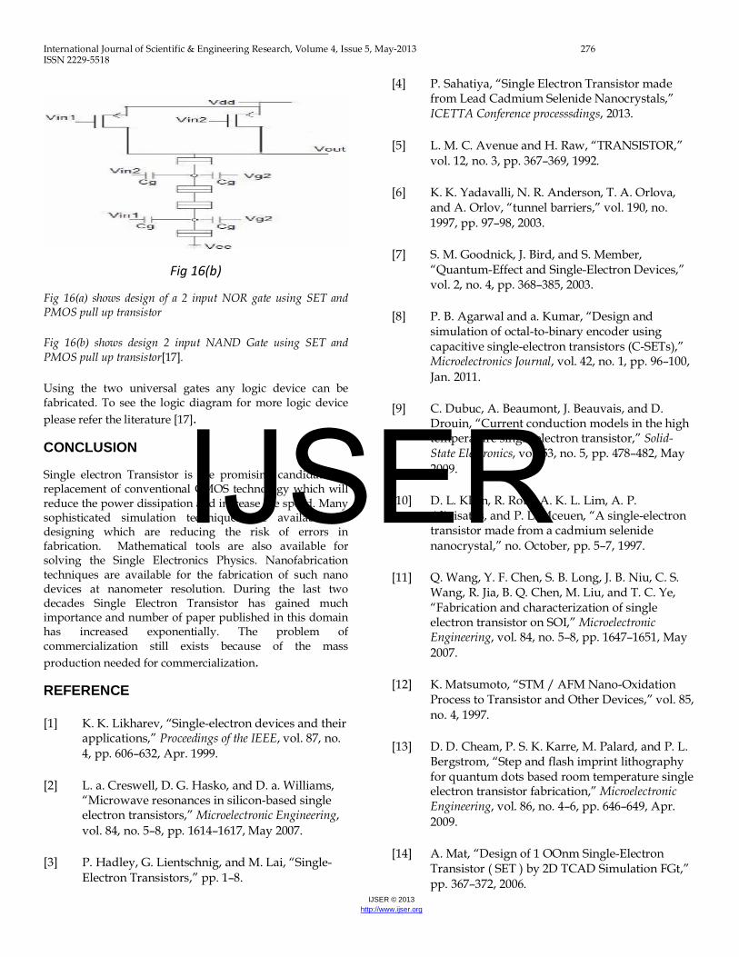
A novel Si memory device is proposed in the literature [16] .The device uses MOSFET and a gateway for electrons transported to and from the memory island . The stored electrons are detected by highly sensitive single electron transistor. The device features ultra low power and high speed operation.
Fig15(a)
Fig 15(b)
Fig 15(a) shows the schematic of Si memory device. Fig 15(b) shows the SEM image of the actual structure corresponding to Fig 15(a)[16].
LOGIC CIRCUITS
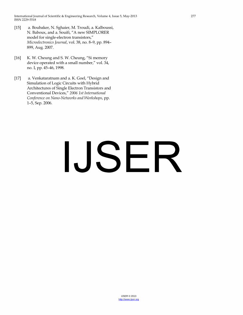
Logic circuits have also been developed using SET which can be used for computation. Many logic circuits like Adder, Encoder including the basic gate have been proposed and fabricated successfully using SET. The Logic devices fabricated using SET has ultra low power dissipation and high speed operation. [17]
Fig 16(a)
IJSER
International Journal of Scientific & Engineering Research, Volume 4, Issue 5, May-2013 276 ISSN 2229-5518
IJSER © 2013 http://www.ijser.org
Fig 16(b)
Fig 16(a) shows design of a 2 input NOR gate using SET and PMOS pull up transistor
Fig 16(b) shows design 2 input NAND Gate using SET and PMOS pull up transistor[17].
Using the two universal gates any logic device can be fabricated. To see the logic diagram for more logic device please refer the literature [17].
CONCLUSION
Single electron Transistor is the promising candidate for replacement of conventional CMOS technology which will reduce the power dissipation and increase the speed. Many sophisticated simulation techniques are available for designing which are reducing the risk of errors in fabrication. Mathematical tools are also available for solving the Single Electronics Physics. Nanofabrication techniques are available for the fabrication of such nano devices at nanometer resolution. During the last two decades Single Electron Transistor has gained much importance and number of paper published in this domain has increased exponentially. The problem of commercialization still exists because of the mass production needed for commercialization.
REFERENCE
[1] K. K. Likharev, “Single-electron devices and their applications,” Proceedings of the IEEE, vol. 87, no. 4, pp. 606–632, Apr. 1999.
[2] L. a. Creswell, D. G. Hasko, and D. a. Williams, “Microwave resonances in silicon-based single electron transistors,” Microelectronic Engineering, vol. 84, no. 5–8, pp. 1614–1617, May 2007.
[3] P. Hadley, G. Lientschnig, and M. Lai, “Single-Electron Transistors,” pp. 1–8.
[4] P. Sahatiya, “Single Electron Transistor made from Lead Cadmium Selenide Nanocrystals,” ICETTA Conference processsdings, 2013.
[5] L. M. C. Avenue and H. Raw, “TRANSISTOR,” vol. 12, no. 3, pp. 367–369, 1992.
[6] K. K. Yadavalli, N. R. Anderson, T. A. Orlova, and A. Orlov, “tunnel barriers,” vol. 190, no. 1997, pp. 97–98, 2003.
[7] S. M. Goodnick, J. Bird, and S. Member, “Quantum-Effect and Single-Electron Devices,” vol. 2, no. 4, pp. 368–385, 2003.
[8] P. B. Agarwal and a. Kumar, “Design and simulation of octal-to-binary encoder using capacitive single-electron transistors (C-SETs),” Microelectronics Journal, vol. 42, no. 1, pp. 96–100, Jan. 2011.
[9] C. Dubuc, A. Beaumont, J. Beauvais, and D. Drouin, “Current conduction models in the high temperature single-electron transistor,” Solid-State Electronics, vol. 53, no. 5, pp. 478–482, May 2009.
[10] D. L. Klein, R. Roth, A. K. L. Lim, A. P. Alivisatos, and P. L. Mceuen, “A single-electron transistor made from a cadmium selenide nanocrystal,” no. October, pp. 5–7, 1997.
[11] Q. Wang, Y. F. Chen, S. B. Long, J. B. Niu, C. S. Wang, R. Jia, B. Q. Chen, M. Liu, and T. C. Ye, “Fabrication and characterization of single electron transistor on SOI,” Microelectronic Engineering, vol. 84, no. 5–8, pp. 1647–1651, May 2007.
[12] K. Matsumoto, “STM / AFM Nano-Oxidation Process to Transistor and Other Devices,” vol. 85, no. 4, 1997.
[13] D. D. Cheam, P. S. K. Karre, M. Palard, and P. L. Bergstrom, “Step and flash imprint lithography for quantum dots based room temperature single electron transistor fabrication,” Microelectronic Engineering, vol. 86, no. 4–6, pp. 646–649, Apr. 2009.
[14] A. Mat, “Design of 1 OOnm Single-Electron Transistor ( SET ) by 2D TCAD Simulation FGt,” pp. 367–372, 2006.
IJSER
International Journal of Scientific & Engineering Research, Volume 4, Issue 5, May-2013 277 ISSN 2229-5518
IJSER © 2013 http://www.ijser.org
[15] a. Boubaker, N. Sghaier, M. Troudi, a. Kalboussi, N. Baboux, and a. Souifi, “A new SIMPLORER model for single-electron transistors,” Microelectronics Journal, vol. 38, no. 8–9, pp. 894–899, Aug. 2007.
[16] K. W. Cheung and S. W. Cheung, “Si memory device operated with a small number,” vol. 34, no. I, pp. 45–46, 1998.
[17] a. Venkataratnam and a. K. Goel, “Design and Simulation of Logic Circuits with Hybrid Architectures of Single Electron Transistors and Conventional Devices,” 2006 1st International Conference on Nano-Networks and Workshops, pp. 1–5, Sep. 2006.
IJSER