Embed Size (px)
Citation preview
Photovoltaics Materials & Device Group, University of Oklahoma: http://www.nhn.ou.edu/~sellers/group/index.html Photovoltaics Materials & Device Group, University of Oklahoma: http://www.nhn.ou.edu/~sellers/group/index.html
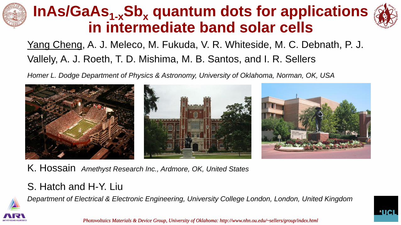
InAs/GaAs1-xSbx quantum dots for applications in intermediate band solar cells
Yang Cheng, A. J. Meleco, M. Fukuda, V. R. Whiteside, M. C. Debnath, P. J.
Vallely, A. J. Roeth, T. D. Mishima, M. B. Santos, and I. R. Sellers
Homer L. Dodge Department of Physics & Astronomy, University of Oklahoma, Norman, OK, USA
K. Hossain Amethyst Research Inc., Ardmore, OK, United States
S. Hatch and H-Y. LiuDepartment of Electrical & Electronic Engineering, University College London, London, United Kingdom
Photovoltaics Materials & Device Group, University of Oklahoma: http://www.nhn.ou.edu/~sellers/group/index.html Photovoltaics Materials & Device Group, University of Oklahoma: http://www.nhn.ou.edu/~sellers/group/index.html
Intermediate Band Solar Cells
2
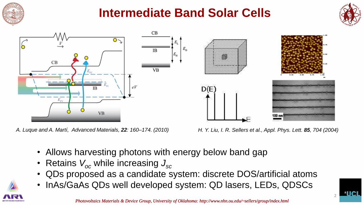
• Allows harvesting photons with energy below band gap
• Retains Voc while increasing Jsc
• QDs proposed as a candidate system: discrete DOS/artificial atoms
• InAs/GaAs QDs well developed system: QD lasers, LEDs, QDSCs
A. Luque and A. Martí, Advanced Materials, 22: 160–174. (2010) H. Y. Liu, I. R. Sellers et al., Appl. Phys. Lett. 85, 704 (2004)
Photovoltaics Materials & Device Group, University of Oklahoma: http://www.nhn.ou.edu/~sellers/group/index.html Photovoltaics Materials & Device Group, University of Oklahoma: http://www.nhn.ou.edu/~sellers/group/index.html
InAs/GaAsSb QD IBSCs
3
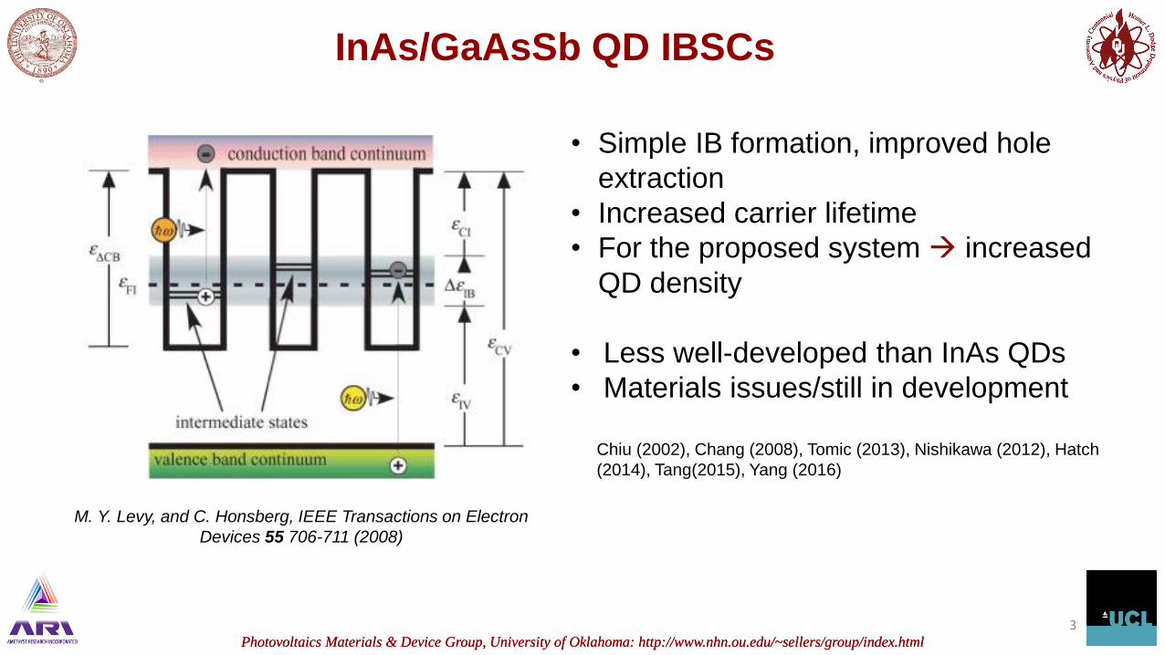
M. Y. Levy, and C. Honsberg, IEEE Transactions on Electron
Devices 55 706-711 (2008)
• Simple IB formation, improved hole
extraction
• Increased carrier lifetime
• For the proposed system increased
QD density
• Less well-developed than InAs QDs
• Materials issues/still in development
Chiu (2002), Chang (2008), Tomic (2013), Nishikawa (2012), Hatch
(2014), Tang(2015), Yang (2016)
Photovoltaics Materials & Device Group, University of Oklahoma: http://www.nhn.ou.edu/~sellers/group/index.html Photovoltaics Materials & Device Group, University of Oklahoma: http://www.nhn.ou.edu/~sellers/group/index.html
Power Dependence of Peak PL
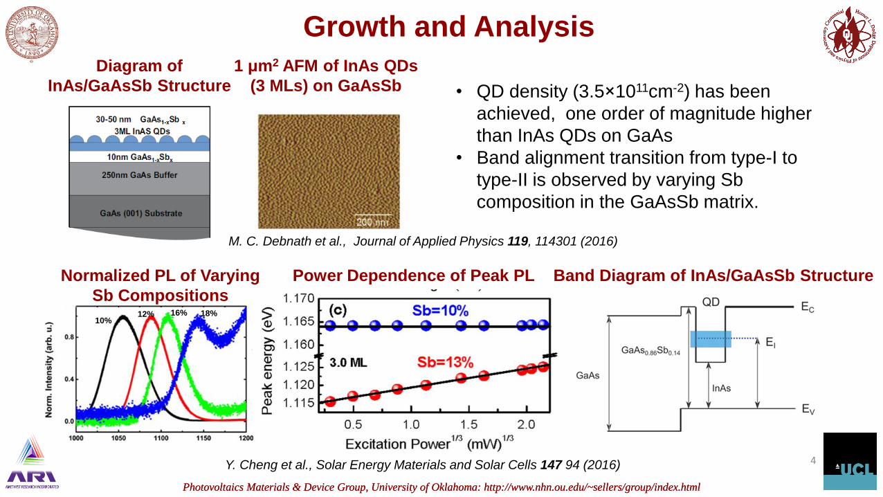
Growth and Analysis
4
• QD density (3.5×1011cm-2) has been
achieved, one order of magnitude higher
than InAs QDs on GaAs
• Band alignment transition from type-I to
type-II is observed by varying Sb
composition in the GaAsSb matrix.
Diagram of
InAs/GaAsSb Structure
1 μm2 AFM of InAs QDs
(3 MLs) on GaAsSb
Y. Cheng et al., Solar Energy Materials and Solar Cells 147 94 (2016)
Band Diagram of InAs/GaAsSb StructureNormalized PL of Varying
Sb Compositions
M. C. Debnath et al., Journal of Applied Physics 119, 114301 (2016)
10%12% 16% 18%
Photovoltaics Materials & Device Group, University of Oklahoma: http://www.nhn.ou.edu/~sellers/group/index.html Photovoltaics Materials & Device Group, University of Oklahoma: http://www.nhn.ou.edu/~sellers/group/index.html
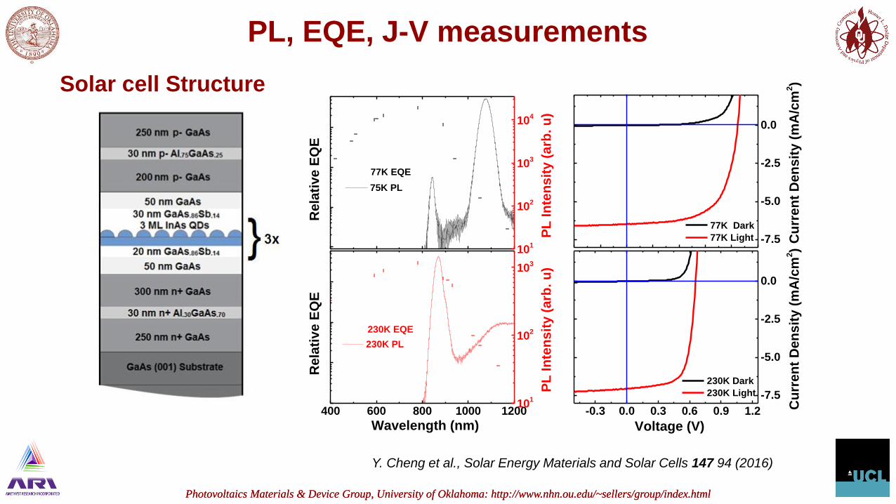
PL, EQE, J-V measurements
Solar cell Structure
Y. Cheng et al., Solar Energy Materials and Solar Cells 147 94 (2016)
-7.5
-5.0
-2.5
0.0
-0.3 0.0 0.3 0.6 0.9 1.2
-7.5
-5.0
-2.5
0.0
77K EQE
Rela
tiv
e E
QE
Cu
rre
nt
De
nsit
y (
mA
/cm
2)
77K Dark
77K Light
400 600 800 1000 1200
230K EQE
Rela
tiv
e E
QE
Wavelength (nm)
Cu
rren
t D
en
sit
y (
mA
/cm
2)
230K Dark
230K Light
Voltage (V)
101
102
103
104
75K PL
PL
In
ten
sit
y (
arb
. u
)
101
102
103
230K PL
PL
In
ten
sit
y (
arb
. u
)

Photovoltaics Materials & Device Group, University of Oklahoma: http://www.nhn.ou.edu/~sellers/group/index.html Photovoltaics Materials & Device Group, University of Oklahoma: http://www.nhn.ou.edu/~sellers/group/index.html
Temperature dependent PL and EQE measurements
10-1
100
101
102
QDs (IB-VB)
GaAsSb
300K90K
Re
lati
ve
EQ
E (
%)
GaAs
800 900 1000 1100 1200
101
102
103
104
210K
75K
Inte
ns
ity
(a
rb. u
)
• GaAs (red arrow) EQE peak shifts
horizontally.
• GaA0.86Sb0.14 (green arrow) EQE peak shifts
to the longer wavelength but also becomes
shallower.
• EQE related to the InAs QDs also has a red
shift, but with an additional enhancement.
• At low temperature, the EQE related to QDs
seems to be dominated by radiative
recombination.
• Reduction of the radiative recombination (PL)
results in the EQE enhancement.
Y. Cheng et al., Solar Energy Materials and Solar Cells 147 94 (2016)
Photovoltaics Materials & Device Group, University of Oklahoma: http://www.nhn.ou.edu/~sellers/group/index.html Photovoltaics Materials & Device Group, University of Oklahoma: http://www.nhn.ou.edu/~sellers/group/index.html
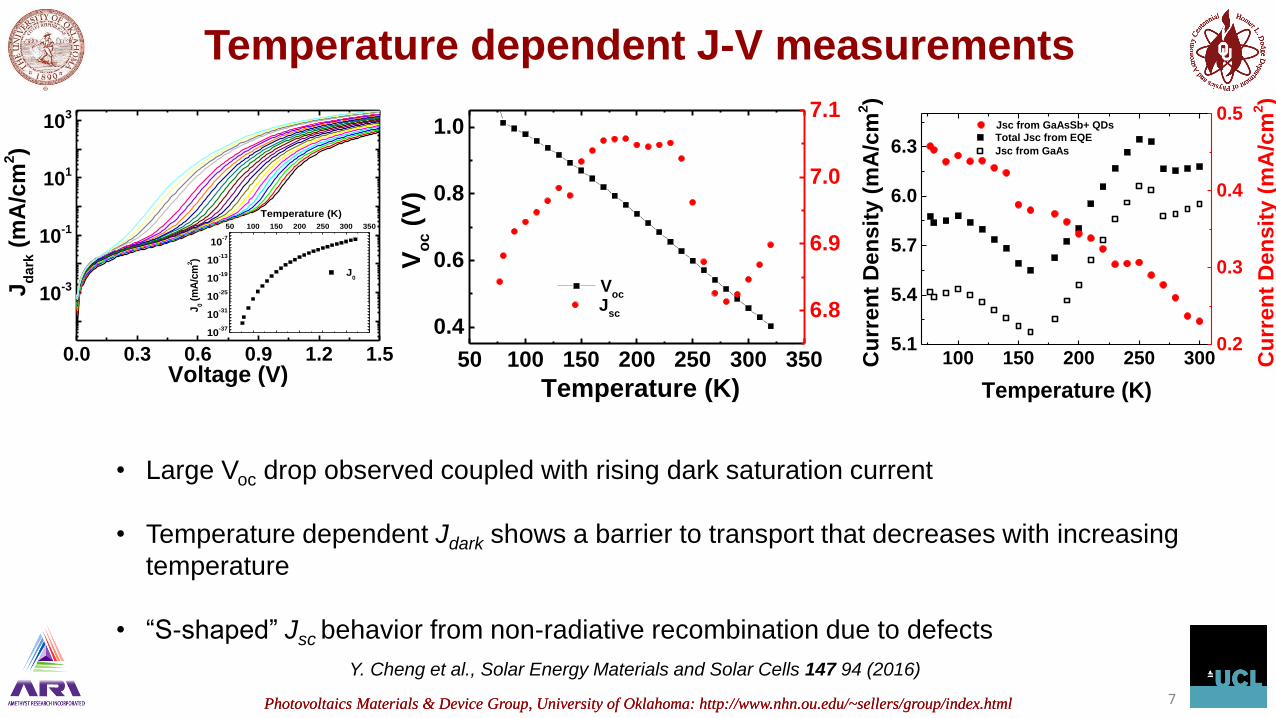
Temperature dependent J-V measurements
7
• Large Voc drop observed coupled with rising dark saturation current
• Temperature dependent Jdark shows a barrier to transport that decreases with increasing
temperature
• “S-shaped” Jsc behavior from non-radiative recombination due to defects
Y. Cheng et al., Solar Energy Materials and Solar Cells 147 94 (2016)
100 150 200 250 3005.1
5.4
5.7
6.0
6.3
Total Jsc from EQE
Jsc from GaAs
Cu
rre
nt
De
ns
ity
(m
A/c
m2)
Temperature (K)
0.2
0.3
0.4
0.5 Jsc from GaAsSb+ QDs
Cu
rre
nt
De
ns
ity
(m
A/c
m2)
0.0 0.3 0.6 0.9 1.2 1.5
10-3
10-1
101
103
10-37
10-31
10-25
10-19
10-13
10-7
50 100 150 200 250 300 350
Temperature (K)
J0
J0 (
mA
/cm
2)
Jd
ark
(m
A/c
m2)
Voltage (V)50 100 150 200 250 300 350
0.4
0.6
0.8
1.0
Temperature (K)V
oc (
V)
Voc
6.8
6.9
7.0
7.1
Jsc
Photovoltaics Materials & Device Group, University of Oklahoma: http://www.nhn.ou.edu/~sellers/group/index.html Photovoltaics Materials & Device Group, University of Oklahoma: http://www.nhn.ou.edu/~sellers/group/index.html
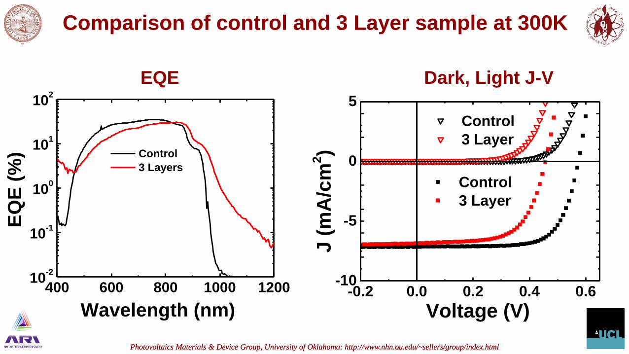
Comparison of control and 3 Layer sample at 300K
Dark, Light J-VEQE
400 600 800 1000 120010
-2
10-1
100
101
102
Control
3 Layers
EQ
E (
%)
Wavelength (nm)
Control
3 Layer
-0.2 0.0 0.2 0.4 0.6-10
-5
0
5
Control
3 Layer
J (
mA
/cm
2)
Voltage (V)
Photovoltaics Materials & Device Group, University of Oklahoma: http://www.nhn.ou.edu/~sellers/group/index.html Photovoltaics Materials & Device Group, University of Oklahoma: http://www.nhn.ou.edu/~sellers/group/index.html
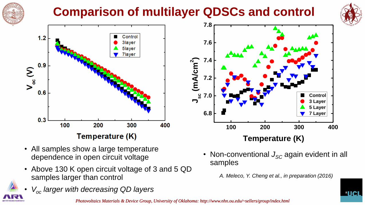
Comparison of multilayer QDSCs and control
• All samples show a large temperature dependence in open circuit voltage
• Above 130 K open circuit voltage of 3 and 5 QD samples larger than control
• Voc larger with decreasing QD layers
• Non-conventional JSC again evident in all samples
A. Meleco, Y. Cheng et al., in preparation (2016)
100 200 300 400
6.8
7.0
7.2
7.4
7.6
7.8
Jsc (
mA
/cm
2)
Temperature (K)
Control
3 Layer
5 Layer
7 Layer
Photovoltaics Materials & Device Group, University of Oklahoma: http://www.nhn.ou.edu/~sellers/group/index.html Photovoltaics Materials & Device Group, University of Oklahoma: http://www.nhn.ou.edu/~sellers/group/index.html
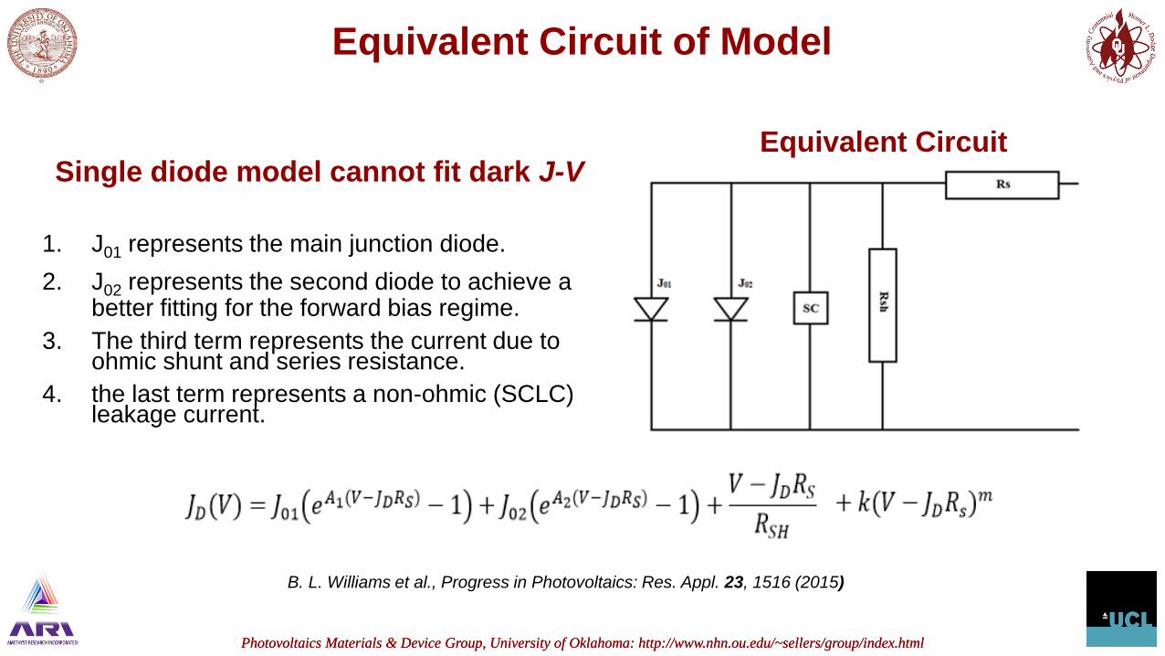
Equivalent Circuit of Model
Single diode model cannot fit dark J-V
1. J01 represents the main junction diode.
2. J02 represents the second diode to achieve a better fitting for the forward bias regime.
3. The third term represents the current due to ohmic shunt and series resistance.
4. the last term represents a non-ohmic (SCLC) leakage current.
Equivalent Circuit
B. L. Williams et al., Progress in Photovoltaics: Res. Appl. 23, 1516 (2015)
Photovoltaics Materials & Device Group, University of Oklahoma: http://www.nhn.ou.edu/~sellers/group/index.html Photovoltaics Materials & Device Group, University of Oklahoma: http://www.nhn.ou.edu/~sellers/group/index.html
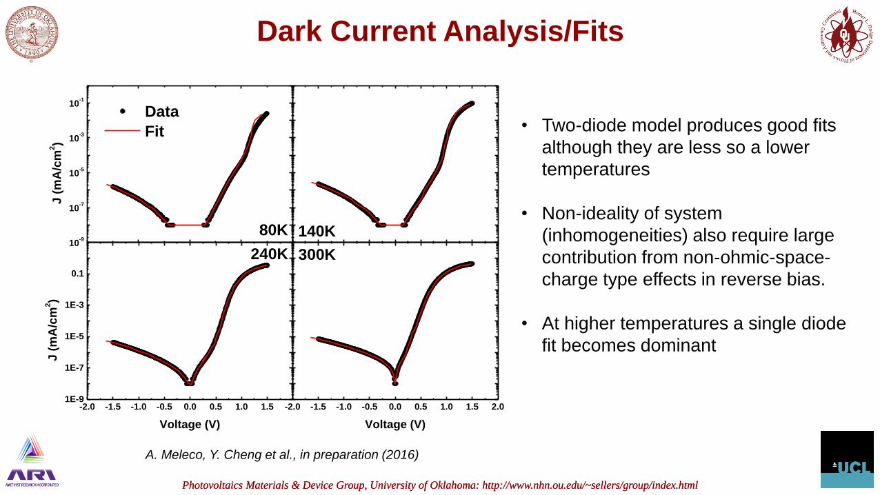
Dark Current Analysis/Fits
10-9
10-7
10-5
10-3
10-1
-2.0 -1.5 -1.0 -0.5 0.0 0.5 1.0 1.51E-9
1E-7
1E-5
1E-3
0.1
-2.0 -1.5 -1.0 -0.5 0.0 0.5 1.0 1.5 2.0
80K
240K
J (
mA
/cm
2)
Data
Fit
140K
J (
mA
/cm
2)
Voltage (V)
300K
Voltage (V)
• Two-diode model produces good fits
although they are less so a lower
temperatures
• Non-ideality of system
(inhomogeneities) also require large
contribution from non-ohmic-space-
charge type effects in reverse bias.
• At higher temperatures a single diode
fit becomes dominant
A. Meleco, Y. Cheng et al., in preparation (2016)
Photovoltaics Materials & Device Group, University of Oklahoma: http://www.nhn.ou.edu/~sellers/group/index.html Photovoltaics Materials & Device Group, University of Oklahoma: http://www.nhn.ou.edu/~sellers/group/index.html
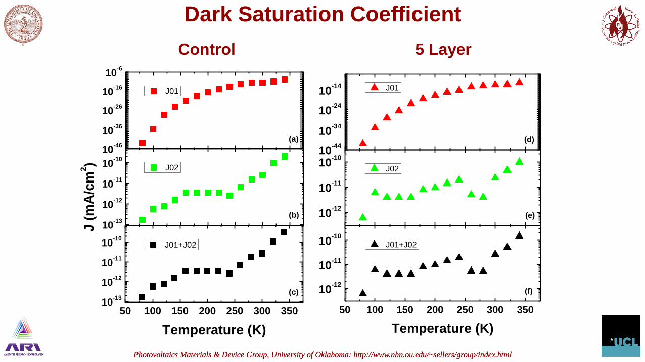
Dark Saturation Coefficient
10-46
10-36
10-26
10-16
10-6
10-13
10-12
10-11
10-10
50 100 150 200 250 300 35010
-13
10-12
10-11
10-10
J01
(a)
(b)
J (
mA
/cm
2) J02
(c)
Temperature (K)
J01+J02
10-44
10-34
10-24
10-14
10-12
10-11
10-10
50 100 150 200 250 300 350
10-12
10-11
10-10
(f)
(e)
(d)
J01
J02
Temperature (K)
J01+J02
Control 5 Layer
Photovoltaics Materials & Device Group, University of Oklahoma: http://www.nhn.ou.edu/~sellers/group/index.html Photovoltaics Materials & Device Group, University of Oklahoma: http://www.nhn.ou.edu/~sellers/group/index.html
Conclusions/Future Work
• Growth conditions for InAs QDs on GaAsSb are optimized. Enhancement of QD density is achieved.
• A transition from type-I to type-II band alignment is observed through power dependent PL measurements.
• Lattice mismatch between GaAs and the matrix contributes to defect formation
• Those defects in the intrinsic region facilitate carrier escape process and dramatically decrease the Voc.
• The escape of electrons compromises the formation of an isolated intermediate band even at low temperature in the present samples
• Phenomenological diode analysis now underway to further elucidate the unusual PV characteristics
• Cross-sectional TEM is important to validate our hypothesis for a defect mediated tunneling model.


![Untitled-2 [] · 2 DOTS 1 DOT 1 DOT POWER BY CYLINDER 2 DOTS 3 DOTS 2 DOTS 2 DOTS ELECTRO-INJECTOR GREEN WHITE RED 6 CYLINDERS TYPE AND 8 CYLINDERS ELECTRO-INJECTORS REFERENCE TABLE](https://img.pdfslide.us/doc/110x75/5f083f2f7e708231d4210fbe/untitled-2-2-dots-1-dot-1-dot-power-by-cylinder-2-dots-3-dots-2-dots-2-dots.jpg)
![Denial-of-Service Open Threat Signaling (DOTS). · architecture, called DDoS Open Threat Signaling (DOTS) [I-D.ietf-dots-architecture], in which a DOTS client can inform a DOTS server](https://img.pdfslide.us/doc/110x75/6018af73a358a566d57c4efb/denial-of-service-open-threat-signaling-dots-architecture-called-ddos-open-threat.jpg)


![ROTHER PRECISION · MSR [option] Battery charger Specification Direct thermal line printing Default : 42cpl 32cpl Option . 48cpl 6), 24cpl Eng : dots, dots Kor : dots dots] Simplified/Traditional](https://img.pdfslide.us/doc/110x75/5fd2b041bcfdb17b192b5e3d/rother-msr-option-battery-charger-specification-direct-thermal-line-printing-default.jpg)