Embed Size (px)
Citation preview
1
Synthesis and Characterization of V-doped β-
In2S3 Thin Films on FTO Substrates
Cristina Tapiaa, Sean P. Berglund
b, Dennis Friedrich
b, Thomas Dittrich
b, Peter Bogdanoff
b,
Yang Liuc,d
, Sergiu Levcenkob, Thomas Unold
b, José Carlos Conesa
a, Antonio L. de Lacey
a,
Marcos Pitaa*, Sebastian Fiechter
b*
a Instituto de Catalisis y Petroleoquimica, CSIC. C/ Marie Curie, 2, L10. 28049 Madrid, Spain.
b Helmholtz-Zentrum Berlin für Materialien und Energie GmbH, Institute for Solar Fuels,
c Helmholtz-Zentrum Berlin für Materialien und Energie GmbH, Nanooptical Concepts for PV,
Hahn-Meitner-Platz 1, 14109 Berlin, Germany.
d Freie Universität Berlin, Institut für Chemie, Fabeckstr. 34-36, 14195 Berlin, Germany
ABSTRACT
Intermediate band semiconductors have raised interest as materials to both enhance
photovoltaics’ efficiency and promote photocatalytic activity driven by visible light. The present
work shows the synthesis of In2S3 doped with four different ratios of V using ILGAR technique.
This nebulize-spray based technique allows the deposition of In2(V)S3 thin layers controlling the
layer thickness and providing high reliability on sample preparation. The samples have been
2
characterized by X-ray diffraction, electron microscopy, profilometry, UV-Vis spectroscopy,
inductively coupled plasma mass spectrometry, X-ray photoemission spectroscopy, surface
photovoltage spectroscopy, time-resolved microwave conductivity, photoelectrochemical
measurements and electrochemical impedance spectroscopy. An optimum of 1.4% V content
yielded the highest enhancement of both photocurrent density and photoluminescence compared
to undoped In2S3. The results suggest that the inclusion of V in the In2S3 at 1.4% yields a high
amount of in-gap levels within the crystalline structure that causes a Fermi energy level shift,
which also induces the shift of the level of both valence and conduction band.
INTRODUCTION
Harvesting energy from the sunlight has been a matter of research for both, its direct conversion
to electricity (via photovoltaic solar cells) and its photochemical possibilities (i.e. photocatalytic
processes). One strategy that can be used to boost the energy collected in the photoabsorption
process is the addition of dopants to semiconductor materials. Dopants cause several effects on
the hosting materials. The most typical effect is influencing the energy band structure of the
hosting semiconductor, broadly known for TiO2 or ZnO.1-3
In some specific cases the dopant
alters the energy level structure of the pure material and causes the appearance of an intermediate
band in its structure. Intermediate band semiconductors became popular few decades ago 2,3
although they were firstly described in 1960.4 Such intermediate band allows the successful
excitation of electrons from the valence band (VB) to the conduction band (CB) in two steps
with photons of energy lower than the fundamental of the host material band gap. The first step
requires a photon with enough energy to excite a valence electron to the intermediate level while
the second step requires another photon with energy to excite the electron again to the CB. In
theory this feature allows solar cell efficiencies above 60%.5,6
3
Based on simulations chalcogenides have been proposed as suitable materials to host an inter-
mediate band by using transition metals as dopants. Such is the case for Ti-substituted III–V
semiconductors,7
Ti- and Cr-substituted CuGaS2 chalcopyrite,8 and SnS2, In2S3 or MgIn2S4
partially substituted by V.9,10
Some of these materials have also been experimentally
synthesized.11,12
In2S3 is a particularly interesting material.13
β-In2S3 has recently been studied as
buffer layer in photovoltaic solar cells because it results in a conversion efficiency very close to
CdS, but it is less toxic.14
β-In2S3 can also play a role in photocatalytic reactions. Advantages of
β-In2S3 for its use as photocatalyst are its band gap energy (Eg ≈ 2-2.3 eV) and its
photoconductivity.14-16
β-In2S3 is an n-type semiconductor with a defect spinel structure where
In3+
occupies tetrahedral positions and S2-
occupies the octahedral positions, or a flowerlike cubic
form.17
It has also been demonstrated that β-In2S3, when properly doped with V, can yield an
intermediate band when synthesized by a hydrothermal route.18
However, to our knowledge V-
doped β-In2S3 has never been synthesized as a thin film on a conductive support.
In this work we demonstrate the deposition and characterization of pure β-In2S3 and V doped β-
In2S3 thin films. Both kinds of thin films were deposited by the Spray Ion Layer Gas Reaction
(Spray-ILGAR) technique;19-21
ILGAR consists on the nebulization of ionic precursors followed
by its gas transport to the heated substrate, where the reaction takes place. In the present paper,
the charge transfer properties of both materials have been characterized using surface
photovoltage spectroscopy (SPV) and time resolved microwave conductivity (TRMC). SPV
provides information regarding the photo-generation of excess charge carriers, their
separation/transport in the bulk and their recombination rate. SPV signals correlate to the specific
region of the material where charge carriers are generated and separated, providing information
about electronic surface states in the bulk and at the different regions measured.21
TRMC is a
4
non-invasive technique that determines the sample photoconductivity providing information
about the mobility and lifetime of the charge carriers. The photoelectrochemical properties of the
material were determined using chronoamperometry under simulated solar radiation, whereas
impedance spectroscopy was used to measure the flat-band potential and incident photon to
current conversion efficiency (ICPE) was measured to determine the dependency of the
photocurrent density on the incident photon energy.
EXPERIMENTAL SECTION
Experimental procedures: deposition and characterization
Reagents. All the reagents were used as received without further purification. Indium
acetylacetonate (In(acac)3), vanadium acetylacetonate (V(acac)3) and ethanol were purchased
from Sigma-Aldrich. Fluorine-doped tin oxide (FTO) cloated glass substrates (~8 Ω/sq) were
received from Solaronix. Sodium carbonate, sodium sulfite and sodium acetate were purchased
from Panreac. Gases used were H2S (5% in nitrogen (N2)) and pure N2.
Deposition of β-In2S3 and V-doped β-In2S3 films. A typical spray-ILGAR set up was used for the
deposition of β-In2S3 and V-doped β-In2S3 films.19
FTO coated glasses and quartz glasses were
used as substrates for the deposition. The temperature of the substrates was kept at 225 °C during
the deposition process. The process and mechanism of β-In2S3 film deposition have been
reported previously.19-21
In this work, the sequential and cyclic Spray-ILGAR process consists of
four steps. First, a solution of In(acac)3 25 mM in ethanol was nebulized to form an aerosol,
Which was blown by N2 gas onto the heated substrate. The H2S (g) flow-rate was 15-20 mL/min
and lasted for 50 seconds. In the second step, the nebulization and H2S flow were stopped for 10
seconds. After that, the H2S flow was introduced into the reaction chamber to react with the film
5
deposited on the heated substrate for 20 seconds. Finally, the H2S gas flow was stopped.
Afterwards, N2 gas flow was used to serve as a purging step for 10 seconds. During all the steps,
the N2 carrier gas flow was set at a constant flow-rate of 5 L/min. These steps of the spray-
ILGAR cycle were repeated until the desired film thickness was obtained.
Different thicknesses of β-In2S3 films were obtained by repeating the Spray-ILGAR cycles 6, 9,
12, 15, 18 or 21 times. These films were used to study influence of the thickness on the optical
properties of In2S3. V-doped β-In2S3 films were deposited by adding 4 different concentrations of
V(acac)2 (0.5, 1, 2 and 10 mM) into the In(acac)3 and ethanol solution and applying 9 Spray-
ILGAR cycles for each case. The process yielded different V percentages: 0.7%V, 1% V, 1.4%
V and 3.4% V respectively. In the case of using quartz substrates, 15 ILGAR cycles were applied
for the deposition of β-In2S3 or V-doped β-In2S3 thin films.
Characterization techniques
X-ray diffraction (XRD) of β-In2S3 and V-doped β-In2S3 was performed with a Bruker D8
Advance X-ray diffractometer (Co-Kα, λ = 0.178897 nm) equipped with a LynxEye detector in a
Bragg-Brentano configuration. The diffractograms were directly measured using the layers as
deposited on the FTO glass substrates as grown.
Scanning electron microscopy (SEM) of the as grown layers was performed using a JEOL JSM
6500F scanning electron microscope.
Transmission electron microscopy (TEM) was applied at a point resolution of 0.19nm with a 200
KV JEOL 2100 transmission electron microscope, equipped with an Oxford Instruments EDX
analyzer. The sample was prepared as follows: a FTO glass substrate modified with 1%V-doped
β-In2S3 was scratched, taking the material powder into an ethanol-filled Eppendorf cap. The
6
sample was immersed for 15 min in an ultrasonic bath. 20 µL of the sample was deposited on a
carbon film coated 200 mesh copper TEM grid (Electron Microscopy Sciences) and let to dry.
The thickness of the β-In2S3 and V-doped β-In2S3 thin films, including variation, was analyzed
using a DEKTAK 8 Advanced Development Profiler (Veeco Instruments).
Inductively coupled plasma mass spectrometry (ICP-MS) was performed using a Hewlett
Packard 4500 Series Shield Torch System spectrometer. The samples were measured without
any further treatment after film deposition.
UV-vis spectra of the modified substrates were measured using a Perkin Elmer Lambda 950
spectrometer equipped with an integrating sphere.
The surface of the thin layer samples was characterized by X-Ray photoelectron spectroscopy
(XPS). XPS measurements were carried out with a monochromatic Al Kα source (Specs Focus
500) and a hemispherical analyzer (Specs Phoibos 100) in an Ultra High Vacuum system with a
base pressure in the low 10-8
mbar range.
Surface photovoltage spectroscopy (SPV). SPV measurements were performed at room
temperature under ambient pressure conditions. The SPV setup and measurement protocol have
been described previously.20-22
The modulated SPV signals were measured using a fixed
capacitor mode. The samples were illuminated with a halogen lamp emitting in the photon
energy range of 0.4 to 4 eV; wavelengths were selected using a quartz prism monochromator.
The monochromatic radiation was chopped at a frequency of 8Hz before illuminating the sample,
and the SPV signal was detected with a double-phase lock-in-amplifier (EG & G, 7260 DSP).21,22
SPV measurements were performed for all the samples.
7
Time-resolved microwave conductivity (TRMC) measurements were performed by mounting the
pure and V doped β- In2S3 samples on quartz substrates in a microwave cavity cell which was
placed within a set-up similar to the one described elsewhere.23,24
The X-band (8.2-12.4 GHz)
microwaves were generated using a voltage controlled oscillator (SiversIMA VO3262X). The
resonance frequency of the loaded cavity containing the sample was determined by measuring
the reflected power as a function of microwave frequency which was normalized with respect to
the power measured for a fully reflecting copper end plate. From the resulting resonance curve
the resonance frequency f0, corresponding to minimum reflected power and maximum electric
field strength within the cavity, was found to be 8.52GHz for our In2S3 films. During the
measurements, a change in the microwave power reflected by the cavity upon sample excitation
by 6 ns (full-width at half-maximum) pulses of a frequency-doubled Q-switched Nd:YAG laser
at a wavelength of 532 nm (10 Hz repetition rate), ΔP/P was monitored and correlated to the
photoinduced change in the conductance of the sample, ΔG, by
where K is the sensitivity factor derived from the resonance characteristics of the cavity and the
dielectric properties of the medium. From the experimentally observed change in the
photoconductance, the product of the charge carrier generation yield (φ) and the sum of electron
and hole mobilities (Σμ) can be obtained according to
DP
P(t) = -KDG(t)
fSµ=DG
I0beFA
8
where I0 is the incident intensity per pulse, e is the elementary charge, β is the ratio between the
inner broad and narrow dimensions of the waveguide, and FA is the fraction of incident photons
absorbed within the sample.
The photoluminescence (PL) measurements were performed using a laser diode (409nm) and a
1/2m grating monochromator equipped with a liquid N2 cooled linear InGaAs diode array and
thermoelectrically cooled CCD array detectors. The PL temperature-dependent measurements
were conducted in a closed-cycle helium cryostat.
Electrochemical and photoelectrochemical characterization was performed using a three-
electrode cell configuration using an aqueous electrolyte containing 0.1 M sodium carbonate, 0.1
M sodium acetate and 0.2 M sodium sulfite at pH 7. A coiled Pt wire was used as counter
electrode, and Ag /AgCl (3M KCl) as reference electrode. Bias voltage to the working electrode
was applied via an electrical contact to the uncoated part of the FTO glass substrate. A surface
area of 0.283 cm2
of the deposited film was in contact with the electrolyte. Photocurrent
measurements were recorded using an EG&G PRINCETON Applied Research Model 273A
potentiostat under white light illumination from a solar simulator (WACOM, type WXS-505-5H)
calibrated to match the AM 1.5 spectrum (100 mW/cm2).
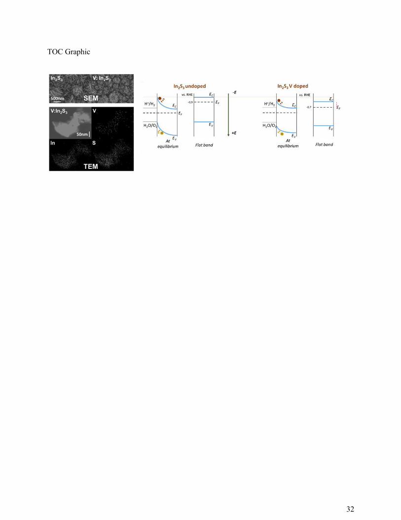
RESULTS AND DISCUSSION
The thin films investigated in the present study were synthesized by the spray-ILGAR, which is
characterized by a sequential and cyclic process to deposit thin layers of metal chalcogenides.
During the first step of the spray-ILGAR cycle the metal ion containing precursor solution is
ultrasonicated to form a mist of droplets. Next the cations dissolved in the mist of droplets are
transported via H2S gas flow to a hot substrate surface (225 °C), where a chalcogenide film is
9
formed by reaction of the metal ions with H2S. In2S3 has been studied as a buffer layer for
chalcopyrite thin film solar cells, but so far it has not been studied as a photoactive
semiconductor alone. For that reason, this work focuses on the preparation and characterization
of In2S3 thin films, doped and undoped, employed as a standalone photoelectrodes. β-In2S3 layers
of different thicknesses were obtained by repeating the ILGAR cycles a various number of times.
The obtained thicknesses were measured using a DEKTAK surface profilometer. It was found
that the thickness of the thin layer increased roughly in proportion with the number of deposition
cycles: 6 cycles yielded a 100nm thick layer, 9 cycles was 350nm, 15 cycles was 700nm, 18
cycles was 910nm, and 21 cycles was 970nm. To prepare V-doped layers 9 cycles were used
with different concentrations of vanadium in the precursor solution (0.5, 1, 2 and 10mM
V(acac)2) yielding approximately 350nm thick layer each. The resulting layers contained an
increasing ratio of V:In. The content of V was measured by ICP-MS, corresponding to 0.7%,
1.0% and 1.4% and 3.4%, respectively.
10
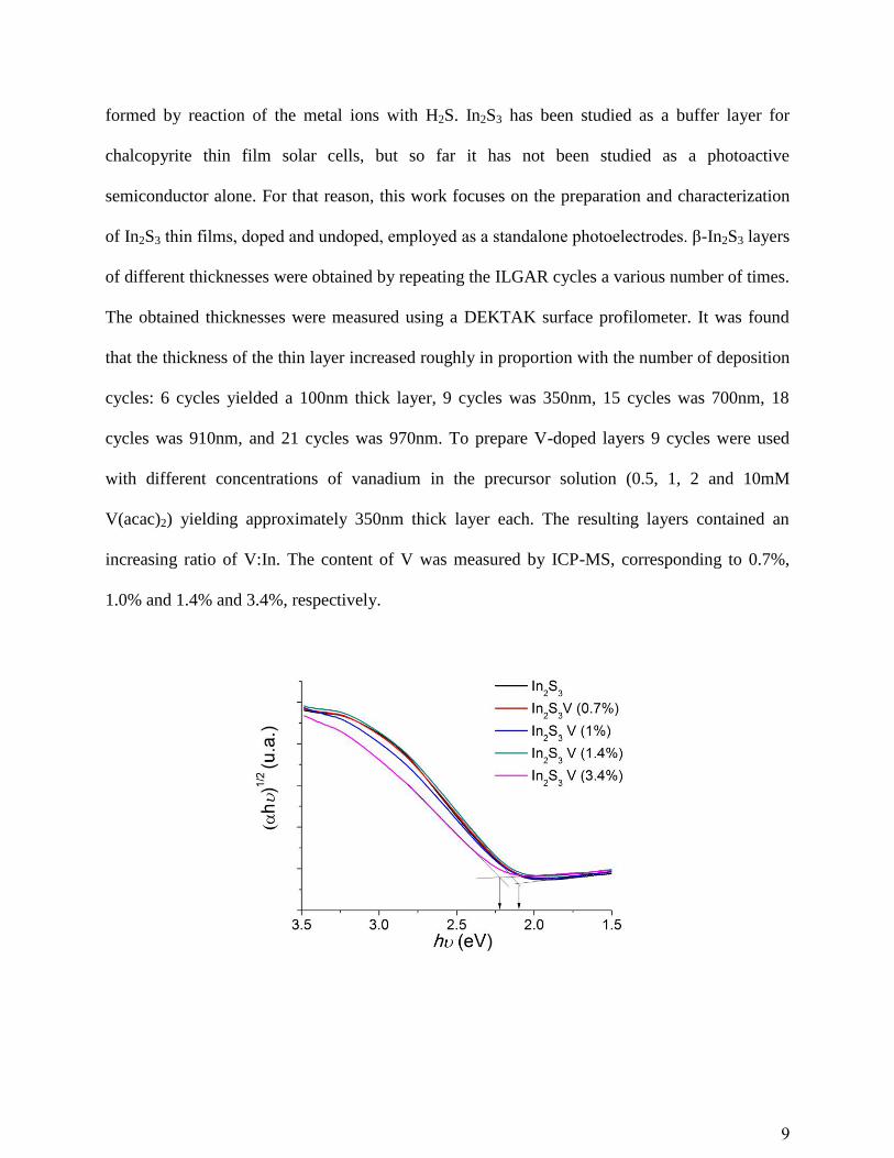
Figure 1. Plot of (αhν)1/2
vs. hν indicating the presence of an indirect band gap of the samples
shown in A.
The crystal structure of the resulting β-In2S3 and V-doped β-In2S3 thin film supported on FTO
were determined by XRD. Figure S1 shows a diffractogram where the peaks corresponding to
the cubic phase of pure β-In2S3 crystals appear.17,25
Vanadium doped and undoped layers did not
show any changes of the cubic diffraction pattern. Only the particle sizes, obtained from the full-
width-half-maxima values employing Scherrer’s formula were different: the undoped β-In2S3
layers exhibited an average grain size diameter of 12 nm, and the V-doped films were evaluated
at 8 nm. These XRD show that the level of V doping studied in this work does not significantly
alter the crystal structure, but does limits the crystal grain size in the films. No additional phase
associated to V is observed in V-doped XRD perhaps due to the low amount of V, but its
formation is not totally excluded (e.g. V2S3). Comparing our results with previously reported V-
doped β-In2S3, where the crystal grains reached 20nm,16
indicates that the synthetic strategy has
an impact on the crystallite size in the final material.
Pure β-In2S3 as well as 0.7%, 1.0%, 1.4% and 3.4% V-doped β-In2S3, all deposited on FTO
substrates, were analyzed by UV-Vis spectroscopy. 0.7-1.4 % V-doped samples displayed a
similar absorption behavior as a function of incident light energy to the pure β-In2S3 sample, but
not the 3.4% V-doped one. From the (αhν)1/m
vs. hν representations an indirect band gap of 2.14
eV for 0.7-1.4 % V-doped and undoped β-In2S3 could be derived, as shown in Figure 1. A
significant increase of the band gap energy is observed for 3.4% V-doped β-In2S3, therefore it
was not further characterized in detail.
11
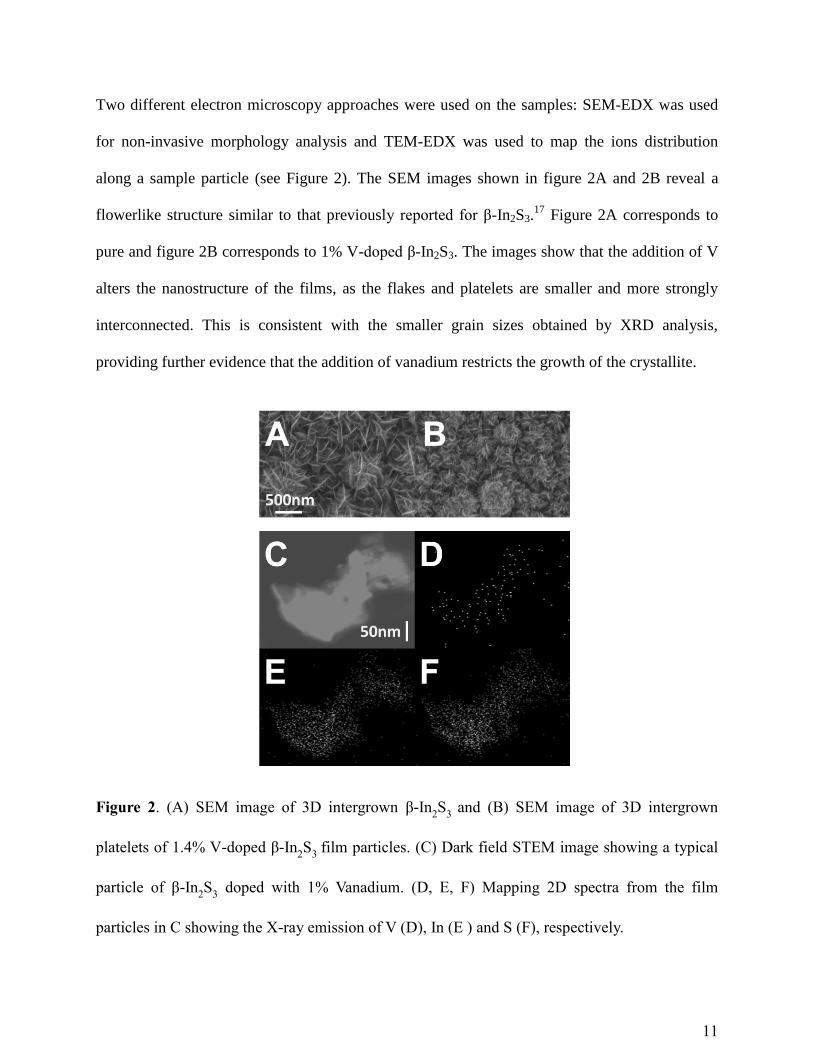
Two different electron microscopy approaches were used on the samples: SEM-EDX was used
for non-invasive morphology analysis and TEM-EDX was used to map the ions distribution
along a sample particle (see Figure 2). The SEM images shown in figure 2A and 2B reveal a
flowerlike structure similar to that previously reported for β-In2S3.17
Figure 2A corresponds to
pure and figure 2B corresponds to 1% V-doped β-In2S3. The images show that the addition of V
alters the nanostructure of the films, as the flakes and platelets are smaller and more strongly
interconnected. This is consistent with the smaller grain sizes obtained by XRD analysis,
providing further evidence that the addition of vanadium restricts the growth of the crystallite.
Figure 2. (A) SEM image of 3D intergrown β-In2S
3 and (B) SEM image of 3D intergrown
platelets of 1.4% V-doped β-In2S
3 film particles. (C) Dark field STEM image showing a typical
particle of β-In2S
3 doped with 1% Vanadium. (D, E, F) Mapping 2D spectra from the film
particles in C showing the X-ray emission of V (D), In (E ) and S (F), respectively.
12
Additional SEM images are available in the supplementary information (Figure S2). EDX
analysis showed an In:S ratio of 2:2.5 for all of the samples, independent of the V content. No V
was detected by EDX in the undoped β-In2S3 sample; however, it was detected in all V-doped
samples. Figure S3 shows EDX typical results for 1% V-doped In2(V)S3 sample, and its
quantitative analysis is shown in Table S1. TEM images were recorded for 1% V-doped β-In2S3
particles that were physically extracted from the FTO surface, dispersed in ethanol, and then
deposited on a TEM grid. The technique known as scanning transmission electron microscopy-
high angle annular dark field (STEM-HAADF) was used to map a typical particle as observed by
TEM, see Figure 2C. The spatial correlation obtained provided evidence of the V, In and S
composition of the particle as shown in Figures 2 D, E, and F.
X-ray Photoemission Spectroscopy (XPS) results
Additional composition analysis of the 1.4% and the 3.4% V-doped β-In2S3 sample was
performed by XPS (Figure S4), a technique that can provide information about bonding and
oxidation state of elements close to the surface (≈ 5 nm) of material. For the 3.4% V β-In2S3
sample, the V 2p3/2 peak is observed at ~517.5 eV (the 2p1/2 peak, broader and less intense,
appears as expected at energy ca 7 V higher); a similar value seems to apply to the 1.4% sample.
There are few literature references on the XPS binding energies of vanadium in a well-defined
sulphide environment. If we consider that V2+
in V2(P2S6) and V3+
in V1.5(P2S6) have been
detected at respectively 514.2 eV and 516.9 eV27
and V4+
in (NR4)2V(dmit)3 has been detected at
523.3 eV28
, one could ascribe the here observed value to a V3+
state, i.e. an isovalent substitution
13
as desired. In this context, the value 514.5 eV reported for V4+
in BaVS3 29
should probably be
considered anomalous.
Surface Photovoltage Spectroscopy (SPV) results
Modulated SPV signals were obtained in-phase (X) and phase shifted by 90° (Y) in relation to
the reference signal. The amplitude of the SPV signal is given as the square root of the sum of
the squares of the X and Y signals [19,20]: √ , while the so-called phase angles is
given by:
.
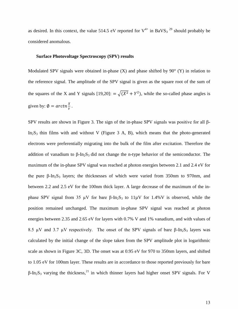
SPV results are shown in Figure 3. The sign of the in-phase SPV signals was positive for all β-
In2S3 thin films with and without V (Figure 3 A, B), which means that the photo-generated
electrons were preferentially migrating into the bulk of the film after excitation. Therefore the
addition of vanadium to β-In2S3 did not change the n-type behavior of the semiconductor. The
maximum of the in-phase SPV signal was reached at photon energies between 2.1 and 2.4 eV for
the pure β-In2S3 layers; the thicknesses of which were varied from 350nm to 970nm, and
between 2.2 and 2.5 eV for the 100nm thick layer. A large decrease of the maximum of the in-
phase SPV signal from 35 µV for bare β-In2S3 to 11µV for 1.4%V is observed, while the
position remained unchanged. The maximum in-phase SPV signal was reached at photon
energies between 2.35 and 2.65 eV for layers with 0.7% V and 1% vanadium, and with values of
8.5 µV and 3.7 µV respectively. The onset of the SPV signals of bare β-In2S3 layers was
calculated by the initial change of the slope taken from the SPV amplitude plot in logarithmic
scale as shown in Figure 3C, 3D. The onset was at 0.95 eV for 970 to 350nm layers, and shifted
to 1.05 eV for 100nm layer. These results are in accordance to those reported previously for bare
β-In2S3 varying the thickness,21
in which thinner layers had higher onset SPV signals. For V
14
doped samples (Fig 3.D) two exponential tails below the band gap were observed. The values for
the first onset SPV signal was at 0.9 eV for the 0.7 %V sample, at 0.95 eV for 1 %V and at 0.8
eV for 1.4 %V. The second onset value was at 1.55 eV for the 0.7 %V sample, at 1.6 eV for 1
%V, and at 1.25 eV for 1.4 %V. These two exponential tails may be due to disordered or deep
defects states added by the presence of vanadium, contributing to the SPV amplitude and caused
by a decrease of disorder. The addition of these defect states in the matrix causes the formation
of an in-gap level in between the conduction and valence band.
Figure 3. SPV signals of a pure β-In2S
3 and V-doped β-In
2S
3 thin films deposited on FTO. The
SPV amplitude (A, B), and SPV amplitude plotted in logarithmic scale (C, D) versus the photon
energy for β-In2S
3 layers of different film thickness as indicate in the figure legend (A,C) and for
β-In2S
3 layers of approximately 350nm thickness doped with 0%V (a), 0.7%V (b), 1%V (c) and
1.4%V (d) (B,D).
15
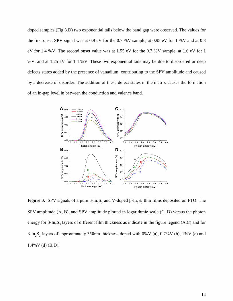
The phase angle contains information about the direction of charge separation and about the time
response of the SPV signal with respect to the modulation period. The phase angles change to -
90° if the time responses of the SPV signals are much slower than the modulation period for
preferential separation of photo-generated electrons towards the internal contact. Phase angles
between -90 and 0° correspond to preferentially modulated separation of photon-generated
electrons towards the bulk. As shown in Figure 4A for the layers without vanadium, the phase
angle changed from -50° at photon energies below 1.5eV to -16° at photon energies between 2.1
and 2.6eV, and decreased again with further increasing of the photon energy. This means that the
modulated response was much slower for the deep defects states. The values of phase angle were
similar for all layer thicknesses studied in the report. However, as shown in Figure 4B, for β-
In2S3 doped with 0.7% V and 1% V no significant change in the phase angle varying the photon
energy from 1.3 to 4eV was observed, remaining at around -45°. For the 1.4% V-doped layer, the
phase angle changed from -80° at photon energies below 1.5eV to -40° at photon energies
between 2.1 and 2.6eV, and decreased again with further increasing photon energy. Thus, it
showed behavior similar to the undoped β-In2S3 layer.
16
Figure 4. Phase angles of β-In2S
3 and V-doped β-In
2S
3 thin films on FTO versus photon energy.
(A) β-In2S
3 films of different thicknesses as indicated in the figure legend. (B) β-In
2S
3 films
doped with 0%V (a), 0.7%V (b), 1%V (c) and 1.4%V (d) (thin films thickness 350 nm).
Time-resolved microwave conductivity results
TMRC is a technique based on the measurement of the change in the reflected microwave power
from the analyzed semiconductor layer after its irradiation with a nanosecond laser pulse that
generates electron-hole pairs. This technique was applied to investigate pure and V-doped β-
17
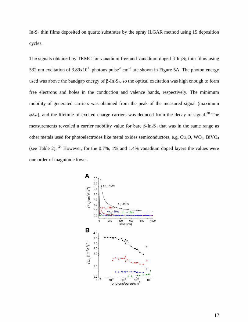
In2S3 thin films deposited on quartz substrates by the spray ILGAR method using 15 deposition
cycles.
The signals obtained by TRMC for vanadium free and vanadium doped β-In2S3 thin films using
532 nm excitation of 3.89x10¹¹
photons pulse-1
cm-2
are shown in Figure 5A. The photon energy
used was above the bandgap energy of β-In2S3, so the optical excitation was high enough to form
free electrons and holes in the conduction and valence bands, respectively. The minimum
mobility of generated carriers was obtained from the peak of the measured signal (maximum
φΣµ), and the lifetime of excited charge carriers was deduced from the decay of signal.30
The
measurements revealed a carrier mobility value for bare β-In2S3 that was in the same range as
other metals used for photoelectrodes like metal oxides semiconductors, e.g. Cu2O, WO3, BiVO4
(see Table 2). 24
However, for the 0.7%, 1% and 1.4% vanadium doped layers the values were
one order of magnitude lower.
18
Figure 5. TRMC signals recorded for pure (a), 0.7% V-doped (b), 1% V-doped (c) and 1.4% V-
doped β-In2S3 versus Time (A) and versus excitation intensity (B).
The microwave conductance transient changed upon doping the β-In2S3 thin layer with
vanadium. At a laser pulse intensity of 3.89x10¹¹
photons/pulse/cm2 the maximum φΣµ for
0.7%V was 0.9 cm2 V
-1s
-1, only 4 times lower than that of the pure material. However, a higher
decrease was observed for 1% V β-In2S3 resulting in a value of maximum φΣµ of 0.2 cm2 V
-1 s
-1,
which is 18 times lower. Sample doped with 1.4% V showed even smaller maximun φΣµ of 0.04
cm2V
-1s
-1 at a laser pulse intesity 2.18x10
12 photons/pulse/cm
2. The lifetime of the carriers was
calculated from the constant of the exponential function used for the fitting. For pure films the
fitting required two constants, which translated into two carrier lifetimes: one of 40ns and
another one that lasts longer (277ns). However, for V-doped β-In2S3 thin films only one constant
was obtained, indicating charge carrier lifetimes of 38 ns for 0.7%V, 29 ns for 1%V and 18 ns
for 1.4%V. Although the lifetimes are lower for the V doped films compared to the pure β-In2S3,
they still are high compared to metal oxide semiconductors.14
The diffusion length decreases
strongly from 619nm for the pure material to 343 nm in the case 0.7% V doped, 150nm on 1% V
and 43 nm on 1.4% V doped β-In2S3 (Table 1). Other oxides values are shown in Table 2. The
decrease of maximum φΣµ must be due to an increase of defects in the matrix explained by the
formation of an in-gap level that contributes to the recombination and trapping of the charge
carriers. The increased doping is not leading to a further lowering of the mobility but evoking a
shorter life time of excited charge carriers. The mobility as a function of excitation intensity,
showed in Figure 5B, is leading to an increase of the mobility of pure samples. This behavior is
explained by assuming a high defect density in the pure material. With increasing light intensity
19
the trap states of the defects in the band are filled leading to a smaller effective mobility. This
behavior could not be found in V-doped layers.
Table 1: Carrier mobility, carrier lifetime and diffusion Length values.
β-In2S
3 Carrier mobility µ (cm
2V
-1s
-1) Carrier
lifetime
(ns)
Diffusion Length
LD (nm)
β-In2S
3 film
type
@3.89x10¹¹
photons/cm2/pulse
@109
photons/cm2/pulse
(extrapolated)
Ʈ1 Ʈ2 LD1 LD2
0% V 3.6 3.7 40 277 619 1630
0.7% V 0.9 1.2 38 - 343 -
1% V 0.2 0.3 29 - 150 -
1.4% V [email protected]
photons/cm2/pulse
- 18 - 43 -
Table 2: Carrier Mobility, Lifetime, and Diffusion Length of Several Metal Oxides
Material Carrier
mobility µ
(cm2V
-1s
-1)
Carrier
lifetime Ʈ
Diffusion
Length LD
(nm)
Fe2O3 0.5 3 ps 2-4
WO3 10 1 – 9 ns 150-500
Cu2O 6 147 ps 25
BiVO4 0.044 40 ns 70
20
Photoluminescence measurements
The Photoluminescence (PL) of β-In2S3 and V-doped β-In2S3 samples show a broad defect
related emission peaked near 1.35eV at 30K (Figure 6A). It can be seen in Figure 6A that PL
yield drops by factor of 3, while the full width at half maximum (FWHM) and the PL maximum
position remain almost unaffected by the V-doping. This implies that the effect of the V defect
level cannot account for the dominant radiative recombination channel in β-In2S3 samples. The
previous studies suggested that donor-acceptor transitions involving VS(donor) and VIn
(acceptor) can be responsible for the broad defect PL band at 1.5 eV in the β-In2S3 single
crystals.31,32
Although in earlier work by Nakanishi et al33
a broad defect band at 1.4.eV in the β-
In2S3 single crystals was revealed, the origin of the radiative transition has not been discussed.
Based on these earlier interpretations it seems reasonable to assume that the observed defect PL
band in β-In2S3 samples is due to S and In vacancies in the host lattice.
Figure 6. (a) Photoluminescence spectra of the doped (green) and pure (red) β-In2S3 layer of
700nm thickness layers recorded at 30 K. (b) Temperature dependent PL of the V-doped β -In2S3
layer (c) the temperature dependence of the PL intensity of the V-doped (green) and pure (red) β
-In2S3 layer.
21
In an attempt to further analyze PL properties and a V-doping effect, temperature dependent PL
measurements have been conducted. As can be noticed in Figure 6B the PL signal is reduced by
one order of magnitude and it is completely quenched for the T>200K in the β-In2S3:V sample as
well as in the pure β-In2S3 one (not shown here). For the both samples the defect related PL band
is shifted to the low energy by about 20meV and broadened by 70meV over the measured
temperature range 30-180K. Figure 6C shows the Arrhenius plots of the integrated PL intensity,
IPL, as a function of the temperature. The solid lines are the least –squares linear fits to the PL
intensity quenching model with two competitive recombination channels34
as IPL =I0/(1+a1exp(-
EA1/kT)+a2exp(-EA2/kT), where I0 is the intensity at the lowest temperature, a1 and a2 are the rate
parameters of the non-radiative process with activation energies EA1 (for T<100K) and EA2 (for
T>100K). We obtained EA1 ≈ 19(16)meV and EA2 ≈ 100(80)meV for the β-In2S3(β-In2S3:V),
samples respectively. The determined EA2 value is in agreement with reported 105meV activation
energy of the defect band at 1.5 eV in the β-In2S3 single crystals.31
According to Ho,30
the 105
meV energy corresponds to the depth of the VIn acceptor level. In the present study by
comparing β-In2S3 with β-In2S3:V sample we observe change of 20 meV in EA2 value, which
might be attributed to the V-doping effect. The lower EA1 energy could not be compared with
earlier reports as low temperature analysis has not been done, but we note that PL quenching has
been observed, too.31
Electrochemical measurements: Flat band potential/Photocurrent/ICPE results
To determine the flat-band potentials of the films, electrochemical impedance spectroscopy
(EIS) measurements were performed and the Mott-Schottky equation was applied, which relates
semiconductor-electrolyte capacitance values to applied potential. During EIS measurements the
applied potential which was varied in the range from -0.4 V to -0.95 V vs RHE, in a buffer
22
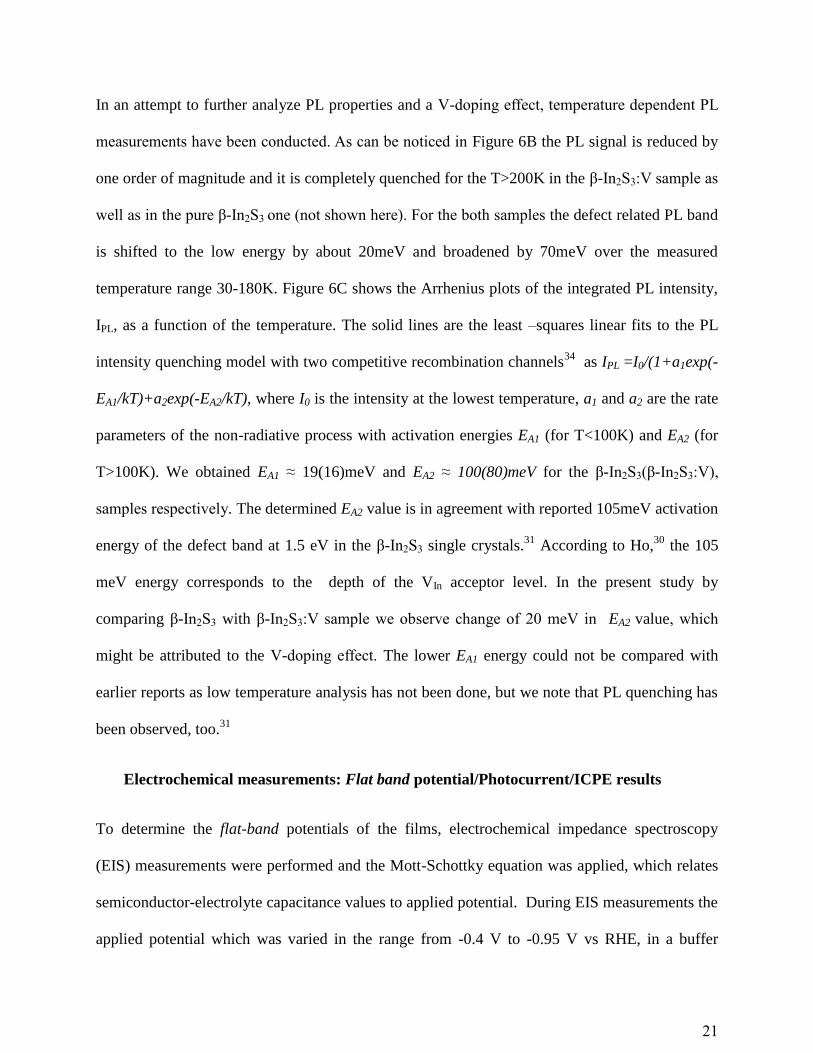
solution at a frequency of 500Hz. Figure 7 shows the Mott-Schottky plot of pure β-In2S3, 0.7% V
β-In2S3, 1% V β-In2S3 and 1.4% V β-In2S3, respectively. A clear shift of at least +0.2 V of the
flat-band potential was measured after doping the β-In2S3 layers with vanadium. It changed from
-0.92 V vs RHE in the case of pure β-In2S3 to -0.70V, -0.68 V and -0.72 V for 0.7% V β-In2S3,
1% V β-In2S3 and 1.4% V β-In2S3 layers, respectively. These shifts in the flat-band potential
suggest that the formation of the in-gap level does shift the valence band and conductive band to
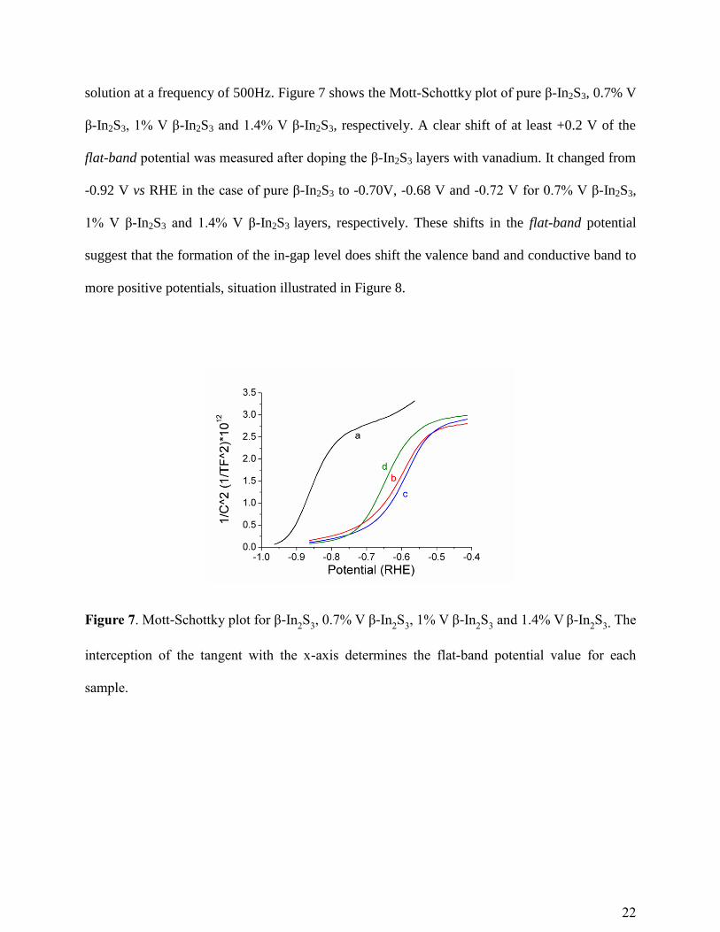
more positive potentials, situation illustrated in Figure 8.
Figure 7. Mott-Schottky plot for β-In2S
3, 0.7% V β-In
2S
3, 1% V β-In
2S
3 and 1.4% V
β-In
2S
3. The
interception of the tangent with the x-axis determines the flat-band potential value for each
sample.
23
Figure 8. Schematic position of the Fermi Level in pure and V-doped β-In2S
3 thin films.
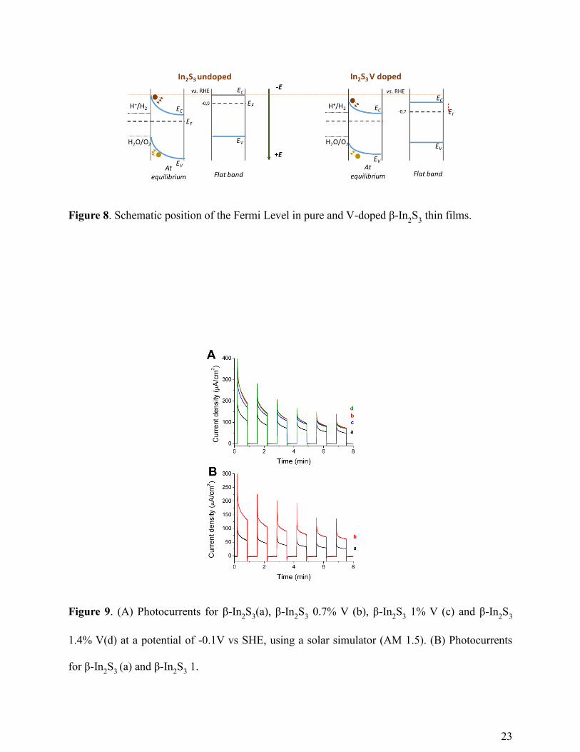
Figure 9. (A) Photocurrents for β-In2S
3(a), β-In
2S
3 0.7% V (b), β-In
2S
3 1% V (c) and β-In
2S
3
1.4% V(d) at a potential of -0.1V vs SHE, using a solar simulator (AM 1.5). (B) Photocurrents
for β-In2S
3 (a) and β-In
2S
3 1.
24
Unfortunately, β-In2S3 thin films on FTO are electrochemically only stable in the potential range
from -1.0 V and -0.40 V vs RHE. In Figure 9A, the photocurrent response of β-In2S3 with and
without vanadium vs time under solar simulator conditions, applying a constant potential of -0.3
V vs RHE, are shown. Processes of recombination were observed in all samples, which were not
affected by vanadium doping. The decrease in photocurrent with time can presumably be
correlated to the corrosion of the material. In all the V-doped samples the photocurrent was
higher than in pure β-In2S3 with no significant difference among the doped samples. To reduce
the corrosion processes at the β-In2S3 electrode surface in contact with the electrolyte, a thin
layer of Cr (4nm) and afterwards of Au (200nm) were deposited consecutively by evaporation
onto the β-In2S3 thin films. Figure 9B shows the photocurrent of the samples covered with gold.
Less corrosion was observed in both pure and V-doped thin layers, but also smaller
photocurrents were measured due to slower diffusion of the holes to the surface. In any case, it is
confirmed that the photocurrents are clearly higher for the V-doped samples up to 1.4% V, but
for the 3.4% V sample the photocurrent decreases (Figure S5), as expected from its higher
indirect band gap.
ICPE measurements were performed with a 300 W power lamp filtered to lower intensity for
specific wavelengths and measured in order to normalize the results. The lowest values were
measured for the 1%V doped sample. In fact, the 1% V β-In2S3 sample was the one that showed
the strongest differences in all the techniques compared to β-In2S3 thin films. The ICPE of all the
V-doped samples decreased strongly compared to pure β-In2S3. One possible reason for this
contrasting behavior may be the much lower light intensity used in the wavelength-resolved
experiments of Figure 10. If the in-gap levels are partially filled (which is the desired situation
for the operation of the intermediate band principle), each one of the two photon absorption
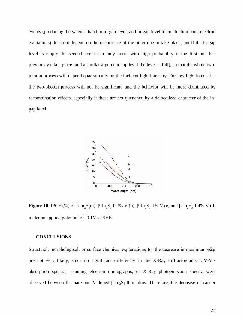
25
events (producing the valence band to in-gap level, and in-gap level to conduction band electron
excitations) does not depend on the occurrence of the other one to take place; but if the in-gap
level is empty the second event can only occur with high probability if the first one has
previously taken place (and a similar argument applies if the level is full), so that the whole two-
photon process will depend quadratically on the incident light intensity. For low light intensities
the two-photon process will not be significant, and the behavior will be more dominated by
recombination effects, especially if these are not quenched by a delocalized character of the in-
gap level.
Figure 10. IPCE (%) of β-In2S
3(a), β-In
2S
3 0.7% V (b), β-In
2S
3 1% V (c) and β-In
2S
3 1.4% V (d)
under an applied potential of -0.1V vs SHE.
CONCLUSIONS
Structural, morphological, or surface-chemical explanations for the decrease in maximum φΣµ
are not very likely, since no significant differences in the X-Ray diffractograms, UV-Vis
absorption spectra, scanning electron micrographs, or X-Ray photoemission spectra were
observed between the bare and V-doped β-In2S3 thin films. Therefore, the decrease of carrier
26
lifetime and diffusion length calculated from TMRC measurements suggests the formation of an
in-gap level which contributes to the recombination and trapping of the charge carriers in V
doped β-In2S3 thin films. These results correlates with SPV results, where a different process for
charge separation was observed for β-In2S3 layers doped with V, suggesting again the formation
of an in-gap level.
Several techniques had been performed to study the photocurrent properties and flat band
potential for β-In2S3 and V doped β-In2S3 thin films. The shift on the flat band potential for the
V-doped samples can be explained by a concentration of defects above the valence band that
shifts the level of the valence and conduction bands to more positive potentials, increasing
lightly the overpotential for electrolyte oxidation. The IPCE measurements suggest that the
formation of the in-gap level increases the charge trapping.
ASSOCIATED CONTENT
Supporting Information. Experimental results containing XRD, SEM, TEM, EDX, XPS
analyses and photocurrent response are provided as Supporting Information. This material is
available free of charge via the Internet at http://pubs.acs.org.
AUTHOR INFORMATION
Corresponding Author
* Marcos Pita, Ph.D. E-mail: [email protected]
Instituto de Catálisis y Petroleoquímica, CSIC
C/ Marie Curie, 2. L10 28049 Madrid, Spain
27
ACKNOWLEDGMENT
The authors thank the Spanish MINECO projects CTQ2012-32448 and CTQ2015-71290-R. CT
thanks the Spanish MINECO for her BES-2013-064099 contract and EEBB-I-16-11240 grant.
REFERENCES
(1) Rehman, S.; Ullah, R.; Butt, A. M.; Gohar, N. D. Strategies of making TiO2 and ZnO visible
light active. J. Hazard. Mater. 2009, 170, 560-569.
(2) Yin, W.-J.; Tang, H.; Wei, S.-H.; Al-Jassim, M. M.; Turner, J.; Yan, Y. Band structure
engineering of semiconductors for enhanced photoelectrochemical water splitting: the case of
TiO2. Physical Review B 2010, 82, 045106.
(3) Tong, H.; Ouyang, S.; Bi, Y.; Umezawa, N.; Oshikiri, M.; Ye, J. Nano-photocatalytic
Materials: Possibilities and Challenges. Advanced Materials 2012, 24, 229-251.
(4) Luque, A.; Martí, A. Increasing the efficiency of ideal solar cells by photon induced
transitions at intermediate levels. Phys. Rev. Lett. 1997, 78, 5014-5017.
(5) Luque, A.; Martí, A. A metallic intermediate band high efficiency solar cell. Prog.
Photovoltaics 2001, 9, 73-86.
(6) Wolf, M. Limitations and possibilities for improvement of photovoltaic solar energy
converters: part I: considerations for earth's surface operation. Proc. IRE, 1960, 48, 1246-1263.
(7) Palacios, P.; Fernández, J. J.; Sánchez, K.; Conesa, J. C.; Wahnón, P. First-principles
investigation of isolated band formation in half-metallic Ti x Ga 1− x P (x= 0.3125–0.25) Phys.
Rev. B: Condens. Matter Mater. Phys. 2006, 73, 085206.
28
(8) Palacios, P.; Sánchez, K.; Conesa, J. C.; Fernández, J. J.; Wahnón, P. Theoretical modelling
of intermediate band solar cell materials based on metal-doped chalcopyrite compounds. Thin
Solid Films 2007, 515, 6280-6284.
(9) Wahnón, P.; Conesa, J. C.; Palacios, P.; Lucena, R.; Aguilera, I.; Seminovski, Y.; Fresno, F.
V-doped SnS2: a new intermediate band material for a better use of the solar spectrum. Phys.
Chem. Chem. Phys. 2011, 13, 20401-20407.
(10) Palacios, P.; Aguilera, I.; Sánchez, K.; Conesa, J. C.; Wahnón, P. Transition-metal-
substituted indium thiospinels as novel intermediate-band materials: prediction and
understanding of their electronic properties. Phys. Rev. Lett. 2008, 101, 046403.
(11) Yu, K. M.; Walukiewicz, W.; Wu, J.; Shan, W.; Beeman, J. W.; Scarpulla, M. A.; Dubon,
O. D.; Becla, P. Synthesis and optical properties of II-O-VI highly mismatched alloys. J. Appl.
Phys. 2004, 95, 6232-6238.
(12) Yu, K. M.; Walukiewicz, W.; Ager, J. W.; Bour, D.; Farshchi, R.; Dubon, O. D.; Li, S. X.;
Sharp, I. D.; Haller, E. E. Multiband GaNAsP quaternary alloys. Appl. Phys. Lett. 2006, 88,
092110.
(13) Lucena, R.; Aguilera, I.; Palacios, P.; Wahnón, P.; Conesa, J. C. Synthesis and spectral
properties of nanocrystalline V-substituted In2S3, a novel material for more efficient use of solar
radiation. Chem. Maters. 2008, 20, 5125-5127.
(14) Dalas, E.; Sakkopoulos, S.; Virtoratos, E.; Maroulis, G.; Kobotiatis, L. Aqueous
precipitation and electrical properties of In2S3: characterization of the In2S3/polyaniline and
In2S3/polypyrrole heterojunctions. J. Mater. Sci. 1993, 28, 5456-5460.
29
(15) Asikainen, T.; Ritala, M.; Leskelä, M. Growth of In2S3 thin films by atomic layer epitaxy.
Applied Surface Science, 1994, 82-83, 122-125.
(16) Kim, W. T.; Kim, C. D. Optical energy gaps of β‐In2S3 thin films grown by spray pyrolysis.
J. Appl. Phys. 1986, 60, 2631-2633.
(17) Chen, L.-Y.; Zhang, Z.-D.; Wang, W.-Z. Self-assembled porous 3D flowerlike β-In2S3
structures: synthesis, characterization, and optical properties. J. Phys. Chem. C 2008, 112, 4117-
4123.
(18) Lucena, R.; Conesa, J. C.; Aguilera, I.; Palacios, P.; Wahnón, P. V-substituted In2S3: an
intermediate band material with photocatalytic activity in the whole visible light range. J. Mater.
Chem. A 2014, 2, 8236-8245.
(19) Allsop, N. A.; Schönmann, A.; Belaidi, A.; Muffler, H.-J.; Mertesacker, B.; Bohne, W.;
Strub, E.; Röhrich, J.; Lux-Steiner, M.C.; Fischer, Ch.-H. Indium sulfide thin films deposited by
the spray ion layer gas reaction technique. Thin Solid Films 2006, 513, 52–56.
(20) Juma, A. O.; Azarpira, A.; Steigert, A.; Pomaska, M.; Fischer, C.-H.; Lauermann, I.;
Dittrich, T. Role of chlorine in In2S3 for band alignment at nanoporous-TiO2/In2S3 Interfaces. J.
Appl. Phys. 2013, 114, 053711.
(21) Juma, A.; Kavalakkatt, J.; Pistor, P.; Latzel, B.; Schwarzburg, K.; Dittrich, T. Formation of
a disorderd hetero‐junction by diffusion of CuI from CuSCN into In2S3 layers: a surface
photovoltage study. Phys. Status Solidi A 2012, 209, 663-668.
30
(22) Duzhko, V.; Timoshenko, V. Yu.; Koch, F.; Dittrich, T. Photovoltage in nanocrystalline
porous TiO2. Phys. Rev. B 2001, 64, 075204.
(23) Kroeze, J. E.; Savenije, T. J.; Warman, J. M. Electrodeless determination of the trap density,
decay kinetics, and charge separation efficiency of dye-sensitized nanocrystalline TiO2. J. Am.
Chem. Soc. 2004, 126, 7608-7618.
(24) Abdi, F. F.; Savenije, T. J.; May, M. M.; Dam, B.; van de Krol, R. The origin of slow carrier
transport in BiVO4 thin film photoanodes: A time-resolved microwave conductivity Study. J.
Phys. Chem. Lett. 2013, 4, 2752−2757.
(25) Fu, X.; Wang, X.; Chen, Z.; Zhang, Z.; Li, Z.; Leung, D. Y.C.; Wu, L.; Fu, X.
Photocatalytic performance of tetragonal and cubic β-In2S3 for the water splitting under visible
light irradiation. Applied Catalysis B: Environmental 2010, 95, 393-399.
(26) Soria, J.; Conesa, J. C.; Granados, M. L.; Mariscal, R.; Fierro, J. L. G.; de la Banda, J. F. G.;
Heinemann, H. Phase transformations of vanadia-titania catalysts induced by phosphoric acid
additive. J Catalysis 1989, 120, 457-464.
(27) Ichimura, K.; Sano, M. Electrical conductivity of layered transition-metal phosphorus
trisulfide crystals. Synth. Metals 1991, 45, 203-211.
(28) Akiba, K.; Matsubayashi, G.-E.; Tanaka, T. Spectroscopic and electrical properties of
oxidized tris(dmit)vanadium anion complexes (dmit = 4,5-dimercapto-1,3-dithiole-2-thionate).
Inorg. Chim. Acta 1989, 165, 245-248.
31
(29) Itti, R.; Wada, T.; Matsuura, K.; Itoh, T.; Ikeda, K.; Yamauchi, H.; Koshizuka, N.; Tanaka,
S. Electronic structure of the BaV 1− x Ti x S 3 system as studied by photoelectron
spectroscopy. Phys. Rev. B 1991, 44, 2306-2312.
(30) Savenije, T. J.; van Veenendaal, P. A. T. T.; de Haas, M. P.; Warman, J. M.; Schropp R. E.
I., Spatially resolved photoconductive properties of profiled polycrystalline silicon thin films. J.
Appl. Phys. 2002, 91, 5671-5676.
(31) Ho, C.-H. Growth and characterization of near-band-edge transitions in β-In2S3 single
crystals. Journal of Crystal Growth 2010, 312, 2718–2723.
(32) Ho, C.H.; Wang, Y.P.; Chan, C.H.; Huang, Y.S.; Li, C. H. Temperature-dependent
photoconductivity in ß-In2S3 single crystals. J. Appl. Phys. 2010, 108, 043518.
(33) Nakanishi, H.; Miyashita, H.; Endo, S.; Irie, T. Photoluminescence and photoconduction in
the system (CdIn2S4) 1-x-(In2S3) x. J. Appl. Phys. 1981, 20, 1481-1486.
(34) Leroux, M.; Grandjean, N.; Beaumont, B.; Nataf, G.; Semond, F.; Massies, J.; Gibart, P.
Temperature quenching of photoluminescence intensities in undoped and doped GaN. J. Appl.
Phys. 1999, 86, 3721.
32
TOC Graphic