Embed Size (px)
Citation preview

1
AAllmmaa MMaatteerr SSttuuddiioorruumm –– UUnniivveerrssiittàà ddii BBoollooggnnaa
DOTTORATO DI RICERCA IN
SCIENZE CHIMICHE
Ciclo XXII
Settore/i scientifico-disciplinare/i di afferenza: CHIM 02
“IN SITU REAL-TIME INVESTIGATION OF
ORGANIC ULTRA-THIN-FILM TRANSISTORS:
GROWTH, ELECTRICAL PROPERTIES AND
BIOSENSING APPLICATIONS”
Presentata da:
Dr. Santiago David Quiroga
Coordinatore Dottorato Relatore
Prof. Giuliano Longoni Prof. Fabio Biscarini
Esame finale anno 2010

2

3
A la memoria de mi madre y de mi abuela; a mi padre y mis tías, Ana y María Dolores.

4

5
Organic electronics has grown enormously during the last decades driven by the encouraging
results and the potentiality of these materials for allowing innovative applications, such as flexible-
large-area displays, low-cost printable circuits, plastic solar cells and lab-on-a-chip devices.
Moreover, their possible field of applications reaches from medicine, biotechnology, process control
and environmental monitoring to defense and security requirements. However, a large number of
questions regarding the mechanism of device operation remain unanswered. Along the most
significant is the charge carrier transport in organic semiconductors, which is not yet well understood.
Other example is the correlation between the morphology and the electrical response. Even if it is
recognized that growth mode plays a crucial role into the performance of devices, it has not been
exhaustively investigated.
The main goal of this thesis was the finding of a correlation between growth modes, electrical
properties and morphology in organic thin-film transistors (OTFTs). In order to study the thickness
dependence of electrical performance in organic ultra-thin-film transistors, we have designed and
developed a home-built experimental setup for performing real-time electrical monitoring and post-
growth in situ electrical characterization techniques. We have grown pentacene TFTs under high
vacuum conditions, varying systematically the deposition rate at a fixed room temperature. The drain
source current IDS and the gate source current IGS were monitored in real-time; while a complete post-
growth in situ electrical characterization was carried out. At the end, an ex situ morphological
investigation was performed by using the atomic force microscope (AFM).
In this work, we present the correlation for pentacene TFTs between growth conditions, Debye
length and morphology (through the correlation length parameter). We have demonstrated that there is
a layered charge carriers distribution, which is strongly dependent of the growth mode (i.e. rate
deposition for a fixed temperature), leading to a variation of the conduction channel from 2 to 7
monolayers (MLs). We conciliate earlier reported results that were apparently contradictory. Our
results made evident the necessity of reconsidering the concept of Debye length in a layered low-
dimensional device. Additionally, we introduce by the first time a breakthrough technique. This
technique makes evident the percolation of the first MLs on pentacene TFTs by monitoring the IGS in
real-time, correlating morphological phenomena with the device electrical response.
The present thesis is organized in the following five chapters. Chapter 1 makes an introduction to
the organic electronics, illustrating the operation principle of TFTs. Chapter 2 presents the organic
growth from theoretical and experimental points of view. The second part of this chapter presents the
electrical characterization of OTFTs and the typical performance of pentacene devices is shown. In
addition, we introduce a correcting technique for the reconstruction of measurements hampered by
leakage current. In chapter 3, we describe in details the design and operation of our innovative home-
built experimental setup for performing real-time and in situ electrical measurements. Some
preliminary results and the breakthrough technique for correlating morphological and electrical
changes are presented. Chapter 4 meets the most important results obtained in real-time and in situ
conditions, which correlate growth conditions, electrical properties and morphology of pentacene
TFTs. In chapter 5 we describe applicative experiments where the electrical performance of pentacene
TFTs has been investigated in ambient conditions, in contact to water or aqueous solutions and,
finally, in the detection of DNA concentration as label-free sensor, within the biosensing framework.

6
Negli ultimi decenni l’organica elettronica ha subito un’importante crescita spinta da diversi
risultati alquanto incoraggianti e dalle potenziali nuove applicazioni che possono dare luogo agli
innumerevoli materiali organici esistenti, tra cui gli schermi flessibili e di grande superficie, i circuiti
stampabili a basso costo, le celle solari plastiche e i dispositivi di tipo “lab-on-a-chip”. Inoltre, i campi
di applicazione sono così vasti da comprendere medicina, biotecnologia, processi di automazione e
monitoraggio dei parametri ambientali, nonché la difesa e la sicurezza. Tuttavia un considerevole
numero di domande deve ancora trovare risposta. Tra queste il meccanismo di operazione, che rimane
senza essere completamente compreso e la correlazione tra la morfologia e la risposta elettrica dei
dispositivi. Nonostante si sia ampiamente riconosciuto l’importante ruolo che il modo di crescita ha
sulla prestazione dei dispositivi, non è stata realizzata un’investigazione esaustiva dell’argomento.
Il principale obbiettivo di questa tesi è quindi quello di trovare una correlazione tra i modi di
crescita e le proprietà elettriche in transistor a film sottile (TFTs) di pentacene. Al fine di studiare la
dipendenza della prestazione elettrica dei TFTs di pentacene al variare dello spessore, si è proceduto
all’ideazione e alla costruzione di una strumentazione sperimentale ad hoc, che permettesse di
realizzare misurazioni elettriche in tempo reale e caratterizzazioni in situ alla fine della deposizione.
Abbiamo provveduto alla crescita di dispositivi TFTs di pentacene in condizione di alto vuoto,
variando metodologicamente la velocità di deposizione a temperatura ambiente prefissata. Durante la
crescita, la corrente di drain IDS e la corrente di gate IGS sono state monitorate in tempo reale e al
termine di ogni deposizione si è proceduto alla caratterizzazione elettrica in situ. Alla fine si è
investigato sulla morfologia ex situ con l’utilizzo di un microscopio di forza atomica (AFM).
Nel presente lavoro si riporta la correlazione valida per TFTs di pentacene tra le condizioni di
crescita, la lunghezza di Debye e la morfologia (quantificata attraverso la lunghezza di correlazione).
Abbiamo dimostrato che i portatori di carica vengono distribuiti nei layers a seconda del modo di
crestita eseguito dal film (che dipende dalla velocità di deposizione per una data temperatura), il quale
porta a una variazione del canale attivo dai 2 ai 7 monolayers (MLs). I nostri risultati hanno conciliato
altri riportati in precedenza, che sembravano alquanto contradittori e hanno evidenziato la necessità di
rielaborare il concetto di lunghezza di Debye in dispositivi a strati a bassa dimensione. Inoltre, per la
prima volta, si presenta un’innovativa tecnica che indica l’avvenimento della percolazione attraverso
il monitoraggio elettrico della IGS durante la deposizione del film sottile, correlando i fenomeni
morfologici con quelli elettrici.
Il capitolo 1 di questa tesi ci introduce nel mondo dell’elettronica organica e ci spiega il
funzionamento del TFT. Il capitolo 2, ci spiega la crescita dei materiali organici, offrendo prima un
fondamento teorico per poi passare alla sperimentazione; dopodiché si esibisce la prestazione elettrica
tipica dei dispositivi di pentacene e si presenta la suddetta tecnica correttiva sugli effetti della corrente
di fuga. Nel capitolo 3 si presenta la strumentazione costruita ad hoc per il monitoraggio elettrico in
tempo reale e in situ; si illustrano inoltre alcuni risultati preliminari, assieme alla suddetta tecnica
“breakthrough”. Intanto, nel capitolo 4, si riportano i più rilevanti risultati ottenuti in tempo reale e in
situ, che correlano il modo di crescita, le proprietà elettriche e la morfologia dei TFTs di pentacene.
Infine, il capitolo 5, si concentra nello studio sulla risposta elettrica dei dispositivi TFTs di pentacene
in contatto con l’ambiente, con acqua e altre soluzioni acquose e, principalmente, della sua
applicazione nella biosensoristica come sensore di concentrazione di DNA.

7
Voglio ringraziare inanzittutto il Dott. Fabio Biscarini per avermi dato la possibilità di svolgere il
mio dottorato di ricerca nel suo laboratorio, per il suo incoraggiamento e per l’appoggio che mi ha
offerto in questi tre anni e per avermi dato una mano e una dritta quando ne ho avuto bisogno. Voglio
inoltre ringraziarlo per la crescita professionale che mi ha permesso di raggiungere in questo periodo
della mia vita.
Voglio ringraziare i miei colleghi del gruppo di organica elettronica: Arian Shehu, Pasquale
D’Angelo, Cristiano Albonetti, Francesco Borgatti, Pablo Stoliar, Andreas Straub e Stefano Casalini.
Ringrazio anche il resto dei colleghi del laboratorio: Francesco Valle, Eva Bystrenova, Beatrice
Chelli, Paolo Greco, Crispin Kegne e Michele Bianchi che, giorno a giorno, si sono resi sempre
disponibili ad aiutarmi e ad offrirmi la loro conoscenza. Ringrazio anche chi oggi non lavora più con
me, ma che ha saputo lasciarmi una parte di sé: Adina Lazar e Matei Iacobini. Ringrazio specialmente
Arian con cui ho lavorato, affrontando le diverse sfide che abbiamo dovuto superare in questo lungo
percorso: grazie a te, non solo per l’appoggio professionale ma, suprattutto, per quello umano. Grazie
perché molti di voi siete diventati non solo bravi colleghi, ma anche veri amici.
Ultimo, ma non meno importante il mio ringraziamento va ai pilastri della mia vita che sono i
miei affetti, la mia famiglia, Paolo e miei amici di sempre: Ariel, Juanjo, Nolwenn, Fer Raballo, Fer
Juárez, Meli, Miguel, Amalia, Sara, Talo e gli amici che l’Italia mi ha regalato in “casa Salvini” e che
mi hanno sostenuto sempre.
Infine ringrazio chi non ho menzionato ma che, in un modo o in un altro, abbia contribuito ad
arricchire la mia vita, permettendomi oggi di essere arrivato fino qui.
Santiago.
Bologna, Marzo 2010

8
Key-Words
Organic Thin Film Transistors
Pentacene
Electrical Characterization
Real-Time Technique
Biosensor

9
1 “Introduction to Organic Ultra-Thin-Film Transistors”
1.1 Organic Electronics: A Brief Review …………………………………………………. 13
1.2 Organic Semiconductors ………………………………………………………………. 14
1.3 Charge Carriers Transport in Organic Semiconductors ……………………………….. 16
1.3.1 Charge Carriers in Organic Semiconductors: n-type and p-type ……………... 16
1.4 Organic Semiconductor Materials for Organic Thin-Film Transistors ……………….. 16
1.5 Operation Principle of Organic Thin-Film Transistors ……………………………….. 18
References ……………………………………………………………………………... 20
2 “Fabrication and Electrical Characterization of Ultra-Thin-Film Transistors”
2.1 Introduction to Organic Growth Dynamics …………………………………………… 21
2.2 Growth Parameters ……………………………………………………………………. 23
2.3 Experimental Setup for High Vacuum Sublimation …………………………………... 24
2.4 Electrical Characterization ……………………………………………………………... 25
2.4.1 Experimental Setup for Electrical Characterization …………………………... 25
2.4.2 Organic Thin-Film Transistor Parameters …………………………………….. 27
2.5 Experimental Results …………………………………………………………………... 29
2.5.1 Electrical Performance of Typical Pentacene TFTs …………………………... 30
2.5.2 Channel Length Effects on the Electrical Response …………………………... 31
2.6 Gate Leakage Effects: A Correcting Technique ……………………………………….. 32
2.7 Conclusions …………………………………………………………………………….. 34
References ……………………………………………………………………………… 34
3 “Real-Time and In Situ Electrical Monitoring of Ultra-Thin-Film Transistors:
Experimental Setup and Techniques”
3.1 Introduction …………………………………………………………………………….. 37
3.2 Samples Architecture …………………………………………………………………... 38
3.3 Sample Cleaning Treatment ……………………………………………………………. 39
3.4 Experimental Setup: The Real-Time and In Situ Growth System ……………………... 40
3.4.1 High Vacuum Chamber and Sample-Holder ………………………………….. 40
3.4.2 Electrical Connections and Software ………………………………………….. 43
3.4.3 High Vacuum Connections ……………………………………………………. 45
3.5 Experimental Techniques and Results …………………………………………………. 45
3.5.1 Electrical Characterization ……………………………………………………. 46
3.5.2 Morphological Characterization ………………………………………………. 50
3.6 Conclusions …………………………………………………………………………….. 51
References ……………………………………………………………………………… 51
Abbreviations & Acronyms ………………………………………………………………. 11

10
4 “Correlation Between Growth Mode, Electrical Properties and
Morphological Parameters”
4.1 Introduction …………………………………………………………………………….. 53
4.2 Experimental Details …………………………………………………………………… 53
4.3 Results and Discussion ………………………………………………………………… 54
4.4 Conclusions …………………………………………………………………………….. 58
4.5 Supplementary Information ……………………………………………………………. 59
References ……………………………………………………………………………… 61
5 “Biosensing Applications”
5.1 Introduction to (Bio-)Field-Effect-Based Sensor Devices ……………………………... 63
5.2 Principle of (Bio-)Organic Thin-Film Devices ………………………………………… 64
5.3 Environmental Stability of Organic Semiconductors ………………………………….. 64
5.3.1 Electrical Response of Pentacene TFTs in Ambient Conditions ……………… 64
5.3.2 Electrical Response of Pentacene TFTs Under Water ………………………… 66
5.4 Biosensors: Pentacene TFTs for the Recognition of DNA Concentration …………….. 69
5.4.1 Experimental …………………………………………………………………... 69
5.4.2 Results and Discussion ………………………………………………………... 70
5.5 Conclusions …………………………………………………………………………….. 73
References ……………………………………………………………………………… 73
Publications …………………………………………………………………………………. 74

11
12
AFM = Atomic Force Microscope
D = Drain
DNA = Deoxyribonucleic Acid
FED = Field-Effect-sensor Device
FET = Field-Effect Transistor
G = Gate
HF = Hydrofluoric Acid
HMDS = 1,1,1,3,3,3 hexamethyldisilazane
HV = High Vacuum
L = channel Length
ML = Monolayer
OTFT = Organic Thin-Film Transistor
S = Source
SAM = Self-Assembled Monolayer
UHQ water = Ultra-High Quality water
UHV = Ultra-High Vacuum
VTH = Threshold Voltage
W = channel Width
= Deposition rate
= Film Thickness/Coverage
= Charge Carrier Mobility
= Correlation Length

13
In this chapter we briefly review the history of the organic electronics, from the first studies on
organic semiconductors, the state-of-the-art until the most recent progress which gives the
perspectives for future investigations. We mainly focus on the physical-chemical properties of the
organic semiconductors and the role they play on the device performance. In addition, the operation
principle of organic thin-film transistors is explained.
1.1 ORGANIC ELECTRONICS: A BRIEF REVIEW
The first studies of electronic properties on organic crystals date back to the early 20th century
[1,2]. In the 1960s, with the discovery of electroluminescence [3,4], the investigation were increased
and the basic models for interpreting the charge carrier transport were established [5,6]. It was not
until the 1970s that the first application of organic semiconductor started, when the conjugated
polymers were successfully synthesized and their doping was controlled [7]. In 1982 the metal-oxide-
semiconductor structure was demonstrated, using polyacetylene as semiconductor and polysilocane as
dielectric [8]. Even if the device has not exhibited a great performance, it was recognized as a
promising technology.
The milestone of organic electronics technology was the demonstration in 1986 of the first
organic field-effect transistor (OFET) or alternatively named organic thin-film transistor (OTFT) [9].
At the same time, the development of organic heterojunction solar cell [10] and organic light emitting
diode [11] were reported. Later on, soluble forms of organic semiconductors were developed, opening
the possibilities to printable circuits [12,13].
Organic electronics technology exhibit comparable performance to amorphous silicon technology
but still remains some order of magnitude lower the performance offered by crystalline silicon
devices. For this reason organic electronics technology is not suitable for high-performance
applications where high switching capability is of primary importance. On the other hand, organic
electronics offers the possibility to deposit a variety of organic materials on a wide range of
substrates, from glass and plastic to paper, by using non-conventional processing techniques, such as
inkjet printing and roll-to-roll manufacturing [14-17]. This alternative technology can be used in a
large number of applications, including flat panel displays [16], organic LEDs [18], photovoltaic cells
[19], radio frequency identification tags [20], large-area electronics [21] and sensors [22].
Before a complete industrialization of this alternative technology becomes a reality, several
aspects of the device reliability need to be solved (i.e. environmental stability, lifetime, etc). Device
reliability lies on a good understand of the electrical properties. Nowadays, the charge carrier
transport in organic semiconductors and the injection phenomenon in the organic/Au and
organic/oxide interface are not well understood. The injection controls the physics of the device, not
only at the molecular level but also microscopically. The comprehension of this interaction is
fundamental to reach a good control of the device characteristics.
We have addressed our studies to the physics of the ultra-thin film transistors, focusing on the
charge carrier transport and the variation of the electrical parameters when the device is exposed to
different environmental conditions (ambient, water and aqueous solutions).

14
1.2 ORGANIC SEMICONDUCTORS
The organic semiconductors can be divided in two main classes:
i) Low molecular weight materials.
ii) Polymers.
Carbon atoms (C-atom) in organic semiconductors form sp2-hybridization (figure 1.1), where
there are three sp2-orbitals on the same plane (each with one electron) and there is a pz-orbital
perpendicular to this plane (with the fourth electron).
Figure 1.1 Scheme of the C atom exhibiting the sp
2 hybridization geometry. The arrow around the atom
indicates the plane on which the sp2 orbitals lie. Three electrons are distributed on the plane in the orbital sp
2,
while the other electron is localized in the pz orbital, perpendicular to the sp2 plane [23].
In an organic semiconductor in which neighboring C-atoms present sp2-hybridization, the overlap
of sp2-sp
2 orbitals forms a covalent strong -bond (figure 1.2 a), whereas the overlap of two pz-
orbitals forms a -bond (figure 1.2 b). The whole molecule has both bonds (figure 1.2 c). By
comparing, the -bonds, which form the backbone of the molecules, are much stronger than the -
bonds. The -bonds are a weaker type of bonding due to the distance between the bonding ( ) and the
antibonding (*), thus the energy levels is lower [24]. On an isolated molecule, the energy levels are
discrete and known as molecular orbitals. The two most interesting molecular orbitals are the highest
occupied molecular orbital (HOMO) and the lowest unoccupied molecular orbital (LUMO). The
energy gap is the difference of energy between them (figure 1.2d).
Molecules, in which neighbouring carbon atoms are sp2 hybridized, forming delocalized clouds
of -electrons, are termed -conjugated. Both low molecular weight and polymers are conjugated
materials. There is some ambiguity in the exact configuration of the bonding structure and the real
molecule is a superposition of all these representations. Figure 1.3 shows two resonance structures of
the polyacetylene.
The -*-transition for conjugated materials has an energy gap which usually varies in the range
1.5-3 eV. For the family of the polyacenes, shown in figure 1.4, the energy gap can be modified
depending on the degree of conjugation in a molecule. The larger the conjugated network is on a
molecule, the smaller the HOMO-LUMO gap will be, because for longer chains the separation
between energy levels is smaller.
One important different between low molecular weight materials and polymers is the possibility
of processing for obtaining thin-films. Small molecules can be deposited by sublimation, while the
polymers can only be processed from solution by spin-coating or printing techniques. A number of
low-molecular materials can also be grown as single crystal, which allows us to investigate the
intrinsic properties [23].

15
Figure 1.2 Ethylene molecule representations: (a) top view, showing the sp
2 orbitals of C-atom (the pz
orbitals are perpendicular to the page), and the s orbitals of the H-atom; (b) -bonds formed by the overlapping
of sp2 orbitals and -bonds formed by the overlapping of pz orbitals; and (c) the whole hybridization; (d) the
energy level.
Figure 1.3 Two resonance structures of the polyacetylene [23].
Figure 1.4 Molecular structure of the first five polyacenes and their predicted and measured HOMO-
LUMO transitions [25]. Note that the C-atom positions for pentacene have been tagged. Positions 6,13 on
pentacene have been identified as the most exposed to oxidation.
Energy Gap
(a) (b)
(c)
(d)

16
1.3 CHARGE CARRIER TRANSPORT IN ORGANIC SEMICONDUCTORS
The presence of extended -conjugated electrons makes possible to design a large variety of both
kinds of organic semiconductors, low molecular weight materials and polymers. Stable molecules
with large, polarisable -systems interact via dispersive forces typically Van deer Waals forces [26]
which are weaker than the covalent bonds in inorganic semiconductors like Si. The organic materials
present a weaker interaction between molecules which allows the transfer of charge carrier from
molecule to molecule. This charge can be moved on along the molecule by applying an electric field,
generating charge states on organic semiconductors. Translated in a band-like picture, this implies a
narrower -band. In terms of charge mobility, it is possible to reach values between 1 and 10 cm2/Vs
in the most perfect molecular crystals. In contrast, in inorganic crystalline semiconductors, charge
carriers move as highly delocalized plane waves in wide energy bands with a very high mobility (~
103 cm
2/Vs). In this case, the mobility is limited by lattice vibrations (phonons) that scatter the carriers
and thus it is reduced as the temperature increases.
In the case of organic thin films, which are technologically relevant, the scenario is even more
complex than in single crystals. Thin-films have the great advantage to be fabricated at low cost with
non conventional techniques. On the other hand, thin-films exhibit lower performance with respect to
single crystals. Highly ordered thermally sublimed oligomers often give rise to polycrystalline films
and solution processed polymers often yield highly disordered or amorphous films. Band transport is
not applicable in this case, due to the presence of structural disorder, large number of defects and
grain boundaries that are intrinsic of thin films. Charge carriers are transported by thermally assisted
hopping between localized states and are scattered at every step. Hopping is assisted by phonons and
the mobility generally increases with temperature. In this case, charge carrier mobility is strictly
connected to the ordering range of the thin-film [26, 27], and it is crucial to find optimized conditions
for the thin-film deposition for improving the long-range ordering and for minimizing defects in the
film structure. Even though there has been a lot of effort in the last twenty years on this argument,
many basic aspects related to the physics of organic semiconductor thin-films remains unclear.
1.3.1 CHARGE CARRIERS IN ORGANIC SEMICONDUCTORS: n-type and p-type
The transport of charge in organic semiconductors typically follows a hopping mechanism and is
governed by the class of transport models related to highly disordered systems. The density of states
of these disordered systems is often asymmetrical and presents a significantly larger barrier to the
formation of one or another type of carrier. Many amorphous or polycrystalline organic
semiconductors sustain either positive or negative charge carriers, but not both.
In conventional, inorganic semiconductor technologies, n-type and p-type refer to the type of
dopant, and therefore majority carrier present in a semiconductor. In crystalline materials both holes
and electrons can usually be transported reasonably well. Disordered electronic systems, on the other
hand, often only support or strongly favor one type of charge carrier and are more properly referred to
as hole or electron transporting. It is, nevertheless, common in the literature to refer to hole
transporting disordered semiconductor materials as p-type and electron transporting materials as n-
type because this describes their majority carriers and semiconducting behavior. An important
complication of both p-type and n-type semiconductors is their poor stability against oxidation and
reduction reactions.
1.4 ORGANIC SEMICONDUCTOR MATERIALS FOR ORGANIC THIN-FILM-
TRANSISTORS
As mentioned above, organic semiconductors are divided in two big groups, polymers and low
weight materials (namely also small molecules). How these elements are connected has a deep
influence on how they are processed and on how they perform. Along the small molecules, pentacene

17
(C22H14) is by far the most popular organic semiconductor. The hydrogen atoms which surround the
carbon backbone are less electronegative than the carbon backbone itself and lend some electron
density to the delocalized electron cloud. The electron rich conjugated molecule has difficulty for
accepting another electron, but is able to lose an electron with a relative ease. As a consequence of
this, positive charge carriers dominate transport in pentacene thin-films. Pentacene is a p-type organic
semiconductor. The density of states and the carrier type are two characteristics which can be
modified by reacting organic semiconductor with strongly electropositive or electronegative materials
such as alkali metals (e.g. K) [28] and metals (e.g. I) [29].
The number of small molecules is practically infinite. Usually, small molecules can be deposited
through thermal sublimation processes, but several of them have been functionalized to be soluble and
can be deposited from solution. The family of acenes and their derivatives shown in figure 1.4, has
fused rings, which are planar and rigid, leading to superior stacking properties. Many of these
materials form polycrystalline films when they are deposited at room temperature. This superior order
allows a better - overlap between the neighboring molecules, improving the overall device
performance. This better performance is made evident through the charge mobility measurement.
Pentacene forms polycrystalline films on insulating substrates (like SiO2), exhibiting good transport
properties. Under appropriated conditions, pentacene and can also form large single crystals [30].
Figure 1.6 Evolution in the OTFTs performance, in term of charge mobility, for different materials
[24,26]. The p-types semiconductors are inside the box. The deposition technique used in each case is indicated
in brackets as: (V) vacuum evaporated, (sc) single-crystal, (S) solution processed. The amorphous hydrogenated
silicon (a-Si:H) mobility is shown as a reference (gray strip).
Pentacene is relatively easy oxidized especially at the 6,13 positions, which disrupt transport and
crystallization on devices (see tagged positions in figure 1.4). This often leads to polymorphic crystal
growth, which can lead to mismatched grains, thus a reduction of the performance. One alternative to
overcome this problem is to synthetically attach bulky groups to the 6,13 positions of pentacene.
When the groups are properly selected this passivates the most reactive sites on the pentacene
molecule and constrain the crystallization into a single highly favorable phase [31].
Figure 1.6 shows the evolution of OTFTs performance, in term of mobility, for several different
p-type and n-type organic semiconductors. The mobility is plotted in logarithmic scale while the time
axis (in year) is plotted in linear scale. It can be seen that mostly of these organic semiconductors
presents charge mobility higher than this one exhibited by the amorphous silicon. The performance

18
depends not only on the material but also on the deposition technique used and the kind of device (p-
type or n-type).
Nowadays, the charge mobility requirements are mostly satisfied but before their
industrialization will be a reality, it is necessary to assure reliability of OTFTs performance under
environmental and working conditions. In this thesis, we will present some experiments in ambient
conditions and in contact to water and other aqueous solutions in chapter 5.
1.5 OPERATION PRINCIPLE OF ORGANIC THIN-FILM TRANSISTORS
Until now, we have made an introduction to the organic materials, the development of organic
semiconductors, focusing on their properties. Moreover, we have shown the evolution of the OTFTs
performance and we introduced the pentacene, which is used in all our experiments presented in this
work. In this section we present the OTFT, including device architecture, operation principle and
modeling of the electrical behavior.
A three-dimensional schematic view of an organic thin-film transistor is shown in figure 1.7. It is
a planar device formed by a gate made of doped-Si (n-type doped Si when the organic material is
pentacene); a dielectric, which is generally made of SiO2; source and drain contacts made of Au; and
the organic semiconductor (in our experiments, pentacene). L is the channel length, the distance
between the source and the drain contacts. W is the channel width, the transverse distance of the Au
structure. Source and drain are isolated from the gate through the dielectric, thus forming a metal-
insulator-semiconductor (MIS) structure. Usually, the Au structure in the channel presents an
interdigitated form, which it is useful for saving space on the substrate (especially for big W).
Figure 1.7 Schematic 3D view of an organic thin-film transistor. In our experiments the organic
semiconductor is pentacene and the dielectric is thermally grown SiO2.
The OTFT is a field-effect device in which the gate voltage VG modulates the charge flow
between source and drain electrodes. In particular, VG induces free charge carriers on the organic
semiconductor, whereas the drain-source voltage VDS, drives these charges from the source contact S
to the drain contact D. The operation principle for a p-type OTFT is illustrated in figure 1.8. Initially,
the OTFT is not connected to any voltage and the structure is comparable to the capacitor (figure
1.8a). When a negative gate voltage is applied, a hole accumulation layer is formed in the
semiconductor adjacent to the dielectric (figure 1.8b). In contrast, if a positive VG is applied, then a
depletion region is formed (figure 1.8c). The accumulated holes can flow from source to drain if a
small voltage between these two contacts is applied (figure 1.8d). Under these conditions the OTFT
operates in linear regime. As the drain voltage becomes more negative VD ≤ VG, a depletion zone will
be formed at the drain side and the channel will be pinched off (figure 1.8 e-f). This condition
corresponds to the saturation regime.

19
Figure 1.8 (a) Schematic of operation of an organic thin-film transistor, using p-type organic
semiconductor: + indicates a positive charges (holes) in the semiconductor, whereas (-) indicates the negative
fixed charge. (b) Creation of a hole accumulation layer when a negative gate voltage VG is applied. (c)
Depletion of holes from the semiconductor, which is indicated by the dotted line, when a positive VG is applied.
(d) Charge flow in the channel due to a difference of voltage applied between source and drain. (e) Creation of a
depletion zone by the drain contact when the drain voltage is more negative than the gate voltage. (f) The
channel is completely depleted from holes because the VG becomes more positive [32].
In a first approximation, the current-voltage characteristics, in linear and saturation regime, can
be modeled through the equations valid also for crystalline silicon FETs [24]:
for: (VGS - VTH) < VDS (1.1)
for: (VGS - VTH) ≥ VDS (1.2)
where Cox is the capacitance of the dielectric per unit area (F/m2), is the charge carrier mobility and
VTH is the threshold voltage. Both electrical parameters and VTH will be explained better in the next
chapter.

20
REFERENCES
[1] J. Koenigsberger, K. Schilling, Ann. Physik 32, 179 (1910).
[2] M. Volmer, Ann Physik 40, 775 (1913).
[3] M. Pope, H. Kallmann, and P. Magnante, J. Chem. Phys. 38, 2042 (1963).
[4] W. Helfrich and W.G. Schneider, Phys. Rev. Lett. 14, 229 (1964).
[5] E. A. Silinsh, Organic molecular crystals. Springer, Berlin 1980.
[6] M. Pope and C. E. Swenberg, Electronic processes in organic crystals, Clarendon Press, Oxford
1982.
[7] C. K. Chiang et al., Phys. Rev. Lett. 39, 1098 (1977).
[8] F. Ebisawa, T. Kurokawa, and S. Nara, J. Appl. Phys. 54, 3255 (1983).
[9] A. Tsumura, H. Koezuka, T. Ando, Appl. Phys. Lett. 49, 1210 (1986).
[10] C. W. Tang, Appl. Phys. Lett. 48, 183 (1986).
[11] C. W. Tang and S. A. VanSlyke, Appl. Phys. Lett. 51, 913 (1987).
[12] K. Y. Jen, G. G. Miller, and R. L. Elsenbaumer, J. Chem. Soc.-Chem. Commun. 17, 1346 (1986).
[13] A. Assadi et al., Appl. Phys. Lett. 53, 195 (1988).
[14] G. H. Gelinck, T. C. T. Geuns, D. M. de Leeuw, Appl. Phys. Lett. 77, 1487 (2000).
[15] S. R. Forrest, Nature 428, 911 (2004).
[16] G. H. Gelinck et al., Nature Mater. 3, 106 (2004).
[17] M. Halik et al., Nature 431, 963 (2004).
[18] J. H. Burroughes et al., Nature 347, 539 (1990)
[19] G. Yu et al., Science 270, 1789 (1995)
[20] E. Cantatore et al., Int. Solid State Circuits Conf. 15.2, 2006.
[21] W. Clemens et al., J. Mater. Res. 19, 1963 (2004).
[22] L. Wang et al., Anal. Bioanal. Chem. 384, 310 (2006).
[23] Ioannis Kymissis, Organic Field Effect Transistors: Theory, Fabrication and Characterization,
Springer, New York, 2009.
[24] Z. Bao, J. Locklin, Organic Field-Effect Transistors, CRC Press, Boca Raton, 2007.
[25] C. W. Scherr, J. Chem. Phys. 21, 1582 (1953).
[26] C. D. Dimitrakopoulos, P. R. L. Malenfant, Adv. Mater. 14, 99 (2002).
[27] W. Brütting, Physics of organic semiconductors, WILEY-VCH, Weinheim (Germany), 2005.
[28] T. Minakata, M. Ozaki, H. Imai, J. Appl. Phys. 74, 1079 (1993).
[29] Y. Matsuo, S. Sasaki, S. Ikehata, Phys. Lett. A 321, 62 (2004).
[30] F.-J. Meyer zu Heringdorf, M. C. Reuter, R. M. Tromp, Nature 412, 517 (2001).
[31] T. N. Jackson et al., Adv. Mater. 15, 2009 (2003).A. R. Brown et al., Synth. Met. 88, 37 (1997).

21
Here the fabrication of organic ultra-thin-film transistors by organic molecular beam deposition
is described. We present a home-made experimental setup for performing electrical characterization
of electronic devices under controlled atmosphere. The extraction of the main device parameters is
detailed. Finally, the electrical characterization of pentacene devices is discussed and a technique for
correcting disturbing effects produced by the leakage current is introduced.
2.1 INTRODUCTION TO ORGANIC GROWTH DYNAMICS
We focus on organic thin-film transistors (OTFTs) grown by organic molecular beam deposition
(OMBD) technique. The growth of organic molecule films is a non-equilibrium phenomenon, where
the growth kinetics plays a crucial role. The organic thin-film growth is complex and this section
presents only a brief description of some features related to our experiments. Figure 2.1 shows
different kinetic processes relevant for the growth by OMBD, such us nucleation, surface diffusion,
and desorption [1]. Classically growth phenomena are classified according to three growth modes
(figure 2.2):
i) Frank-van-der-Merwe or layer-by-layer.
ii) Stranski-Krastanov (layer-by-layer and, above a critical thickness, island
growth).
iii) Vollmer-Weber or island growth (from the first monolayer). This can also
occur following nucleation of crystalline nuclei with no preferred
crystallographic orientation on the basal plane.
The growth modes can be described using different arguments, such as epitaxy and the surface
and interface energies. The epitaxy refers to systems where there is a commensurate relationship
between the molecular positions in the growing layer and the substrate. Epitaxy often is accompanied
by a lattice mismatch between the film and the substrate, which is not only important from the
crystallographic point of view, but also influences the growth beyond the first monolayers [2]. This
suggests that by a proper selection of the substrate the crystal structure of the epitaxial layers can be
controlled from the first ML (adjacent to the substrate) to higher layers [3]. In the case of molecular
semiconductors, this concept is useful to understand the organization of the molecules at the metal-
semiconductor interface in devices, although the metal films are polycrystalline. In the channel, usual
dielectric surfaces (e.g. silicon oxide) are amorphous and the concept does not apply.
Another approach to describe the various relevant interactions uses the concept of surface and
interface energies. The relevant surface energies are: the free substrate surface, s, the film surface, f ,
and the film-substrate interface, i. Depending on these energies, the thin-film growth follows one of
the three growth modes described above. Surface energy plays an important role in the growth of
organic semiconductors both on the metal electrodes and on the dielectric channel. Several works
have reported the use of different methodologies for changing the substrate surface energy, thus

22
modifying the growth mode. One of the most common approaches is the use of self-assembled
monolayers (SAMs) [4-6].
Figure 2.1 Schematic of dynamic processes relevant in the thin-film growth by organic molecular beam
deposition technique [7].
There are some other considerations concerning the organic growth exclusively:
i) The internal degrees of freedom: molecules should be considered as objects
with orientational and vibrational degrees of freedom. The orientational
degrees of freedom are related to changes of the molecular orientation during
the growth (lying-down and standing-up). The vibrational degrees of freedom
affect the interaction with the surface as well as the thermalization and the
diffusivity [8].
ii) The Van-der-Waals interactions are more important, thus implying that
relevant temperature scales for sublimation, diffusion, annealing are lower. It
is important to mention that for reactive surfaces the diffusion is limited and
then the reorganization of the film is hampered. In the extreme case of very
reactive surfaces, the molecules can dissociate upon adsorption [9,10].
iii) In addition to the sources of disorder known from inorganic system (i.e.
vacancies), organics frequently crystallize in low-symmetry structures, which
can lead to multiple domains, which further increases the disorder o [8].
Adsorption

23
Figure 2.2 Growth modes of organic thin-films grown by OMBD, from the point of view of the surface
and interface energies: layer-by-layer, layer plus island and island growth.
2.2 GROWTH PARAMETERS
Pentacene is the most studied organic semiconductor, owing to its excellent properties as active
layer in OTFTs [11]. Morphological scaling analysis on sub-ML thin-films have shown that the
smallest stable nucleus is composed of four molecules [12]. Single crystalline island size can reach
0.1 mm [13]. Pentacene films show two different polymorphic structures: Campbell’s or “bulk” phase
[14] and the so-called “thin film” or Holmes phase [15]. Recently, a controversial third pentacene
polymorph present in thin-films with enhanced physical properties has been reported by Siegrist et
al.[16]. For thicker films, the Holmes and Campbell phases coexist depending on the growth
conditions [17]. The bulk crystalline structure is shown in figure 2.3.
We focus on the study of pentacene thin-film growth on SiO2. In order to achieve a high
performance of pentacene devices, it is crucial to have a control of the morphology, [18,19]
optimizing the thin-film organization, and minimizing the structural defects [20]. The growth mode
and the film morphology are strongly dependent on the following parameters:
i) Deposition rate [2 23 .
ii) Substrate temperature Tsubstrate [23].
iii) The surface energy [24].
iv) The kinetic energy of the incident molecules [25].
Verlaak et al. [24], have studied the thermodynamics of nucleation for pentacene on
technologically-relevant substrates such as SiO2 with and without different primers, as a function of
Tsubstrate and . The nucleation phase diagram is shown in figure 2.4(a). By inspection of the phase
diagram, it can be noted that only films grown below the dotted line (2D nucleation) can grow in a
layer-by-layer mode. Since growth mode depends also on the surface energy and roughness, there can
be a transition to 3D growth, with enhanced stacking of monolayer terraces before the completion of
the underlying layers as the film grow. This is frequently observed in the case of pentacene, and the
phenomenology can be ascribed to the spatial dependence of the van der Waals interaction between
the condensing molecules and the growing islands with increasing thickness. In fact, many layers are
needed to reach a saturation in the spatial dependence of the interaction. This affects on one hand the
surface energy, and hence the nucleation rate and nuclei dimensionality. On the other hand, it also
affects the self-diffusional barriers including the Schwoebel barrier. The latter is the energy barrier for
molecules to diffuse across a terrace edge, which would lead to smoothening of the stacked structures
and the completion of the underlying layers. The increase of the Schwoebel barrier vs thickness leads
to enhance the effective upward flow of molecules which accounts for the 3D stacking. Ruiz et al.
have developed a kinetic model based on Master equation to predict the evolution of pentacene films
[26]. The parameters of the model are the diffusional rates across the pentacene surface, and time is
renormalized to the inverse deposition rate. The evolution of the occupancy, which is the coverage of
each monolayer, is shown in figure 2.4(b). The model can be parameterized by fitting X-ray scattering
[27] or AFM roughness dynamic scaling data [28]. The outcome of the model is that at the early
stages growth occurs layer-by-layer, viz. no upper layer starts growing before the completion of the

24
underlying monolayer. Above 1-2 monolayers, the stacking of incomplete layers starts and get
enhanced as thickness grows. For instance the growth of the fourth monolayer starts at the completion
of the second ML and finishes after 5 MLs have been deposited. The fifth monolayer appears at 2.5
ML nominal thickness and is completed beyond 6 ML. This is in agreement with the roughness
scaling vs thickness reported in ref. [29, 30].
Figure 2.3 (a-b) Bulk (Campbell’s) crystalline structure of pentacene [14]
Figure 2.4 (a) Growth modes for pentacene assuming ψmol-sub = 0 (interaction strength between one
molecule and the substrate is zero) [24]. Below the solid line, three-dimensional (3D) nucleation is
possible. For growth conditions below the dashed line, two-dimensional (2D) nucleation is possible. 2D
nucleation becomes more likely than 3D nucleation only below the dotted line. In a first approximation,
only growth conditions below the dotted lines will give rise to continuous films. (b) Evolution of the
coverage as a function of the film thickness for pentacene on SiO2 [26].
2.3 EXPERIMENTAL SETUP FOR HIGH-VACUUM SUBLIMATION
The organic growth of molecules like pentacene or sexithienyl is performed by sublimation in an
experimental setup composed of: high vacuum (HV) chamber, Knudsen cell, quartz crystal
microbalance, shutter and sample-holder. In this chapter we describe the main experimental setup
used in our group (figure 2.5a). In chapter 3 we present a more complex experimental setup, built
during this thesis, which allows us to carry out a series of characterization experiments in real-time
and in situ conditions.

25
The Knudsen cell is composed of: quartz crucible, containing the organic semiconductor, and a
heating Tungsten wire. The temperature of the crucible is increased by a PID controller. The
particular geometry of each Knudsen cell and its position and orientation in the HV chamber
determine the deposition rate measured near the sample at a certain temperature of the crucible.
During the calibration of the quartz crystal microbalance, we correlated the temperature of the
crucible to the deposition rate (figure 2.5 b). The substrate temperature is monitored through a
thermocouple mounted on the sample-holder and can be also increased by using a second PID.
For our experiment we use pentacene (Fluka-N° 45797). Purification of organic materials is
essential for assuring that the grown thin-film is reasonably free of impurities which may act as traps
or dopants in an electronic device [10]. There are several techniques for purification. The simplest
technique is the outgassing, which is what we used. Another popular technique is the gradient
sublimation, which is more sophisticated [31]. Outgassing consists of heating the organic material
close to the sublimation point in HV for a few hours. This allows removal the traces of solvent and
smaller oligomers or lighter precursors. The absence of H2O and O2 in HV minimize thermal
degradation of the material. Once outgassed, pentacene is kept under HV. Growth in a HV
environment assures that a minimal density of impurities and defects will be incorporated into the
film. The degree of impurities which may be deposited on the substrate depends on the quality of the
vacuum and the deposition rate, as slower rates occur in longer time [10].
Figure 2.5 (a) HV sublimation chamber. The main elements are: (1) HV chamber; (2) Knudsen cell; (3)
quartz crystal microbalance; (4) sample-holder manipulator; (5) shutter; (6) fast-entry; (7) viewport + light, for
optical monitoring; (8) connections to turbomolecular and scroll pump. (b) Rate of deposition vs pentacene
temperature as measured from a calibrated quartz crystal microbalance.
2.4 ELECTRICAL CHARACTERIZATION
The electrical characterization of OTFTs is a fundamental tool for investigating charge transport
phenomena in organic materials. OTFTs are quite sensitive to the environmental conditions at which
they are exposed. For this reason a special experimental setup for performing electrical
characterization under controlled atmosphere was built. In chapter 5 we will present and discuss
experiments related with OTFTs applications in the biosensing field in which the devices are exposed
to aqueous solutions.
This section dedicated to the electrical characterization of organic ultra thin-film transistors is
divided in two parts. In the first part we outline the home-made experimental setup for electrical

26
characterization and the second part is focused on the techniques for extracting electrical parameters,
in which we are interested.
2.4.1 EXPERIMENTAL SETUP FOR ELECTRICAL CHARACTERIZATION
We have designed and mounted a home-built experimental setup to investigate the electrical
response of OTFTs in either high vacuum HV or inert gas atmosphere. All parts of this system were
entirely designed and assembled at the CNR-ISMN laboratories, and some critical components were
manufactured in CNR machine shop. The system is shown in figure 2.6. It consists of a HV chamber
(1) with front entry (2); a top viewport for optical monitoring (3) of the inside through a video camera
(4); feedthroughs for gases (controlled by leak valves) and the electrical connections.
Figure 2.6 Integral system for electrical measurements under controlled atmosphere. (a) Main view: (1)
HV chamber; (2) front entry; (3) viewport; (4) video camera; (5) pumping connection. (b) Top view. The sliding
tray (6) is visible inside the HV chamber. (c) Interior view of the HV chamber showing the test pattern (7) and
the piezoelectric motors (8). (d) View of a test pattern; the probes (9) which are connected to the piezoelectric
motors are approached on the source and drain contacts by means of a video-assisted joystick which moves the
piezoelectric motors.
The samples are introduced in the HV chamber from the front entry. The feedthroughs and other
electrical connections, vacuum gauges and thermocouples for monitoring the temperature in different
points inside the HV chamber, are located at the backside. The pumping system (5) consists of a
turbomolecular pump (Varian TV81-M) coupled to a scroll pump. The minimum base pressure
obtained with the scroll pump is 1 mbar. With the turbo molecular pump in regime the pressure can go
down to 10-4
mbar. Inside the HV chamber there is a sliding tray (6) with a platform on top, which
contains a Peltier element for increasing or decreasing the substrate temperature Tsubstrate in the range
0-150°C. On this platform, an electromechanical system was mounted. This electromechanical system
consists of three actuators (8), each carrying an etched W probe (9) connected to a feedthrough. Each
actuator is made of three piezoelectric motors (Physik Instrumente, PILine®
M-6624V0X), one for

27
each axis in space. The probes can be positioned independently with submicrometer accuracy. The
probe positioning is remotely controlled by a dedicated software, a joystick and a video camera. The
motor drivers are located outside the chamber in a separate rack.
The test pattern (7) is placed on the tray and the three probes are landed on the substrate for
contacting source, drain, gate electrodes to the external measurement unit outside the HV chamber
(figure 2.6 d). Once the desired environmental conditions are reached the electrical characterization is
performed. Coaxial cables are used for connecting the probes to the external measurement unit, in
order to reduce environmental electrical noise. The measurement unit consists of a general purpose
dual channel source/meter unit Keithley 2612, which is remotely controlled by a dedicated software.
The electrical connections of the three probes to the measurement unit are schematically shown in
figure 2.7.
Figure 2.7 Connection of Keithley 2612 source/meter unit to the integral system for electrical
measurements under controlled atmosphere. The gate probe is connected to the HI terminal of channel A, the
drain probe is connected to HI terminal of channel B, and the source probe is connected to both LO terminals of
channel A and channel B.
2.4.2 ORGANIC THIN-FILM TRANSISTOR PARAMETERS
According to eq. 1.1 and 1.2 the drain source current IDS depends on two independent voltages,
the drain source voltage VDS and the gate source voltage VGS. For this reason, the current-voltage
curves can be plotted in two different ways:
i) Output characteristics (figure 2.8 a).
ii) Transfer characteristics (figure 2.8b).
In the first case, a set of drain source current is plotted as a function of drain source voltage for a
range of gate source biases; in the second case, the drain source current is plotted as a function of the
gate source voltage for a fixed drain source voltage.
From the output curves the regime of operation can be identified, i.e. linear or saturation
regime. Then the transfer characteristics are acquired in linear and saturation, in order to extract the
following parameters: mobility m, threshold voltage VTH, subthreshold slope, ON/OFF ratio and
pinch-off voltage. All these parameters were extracted by using standard procedures, below described.
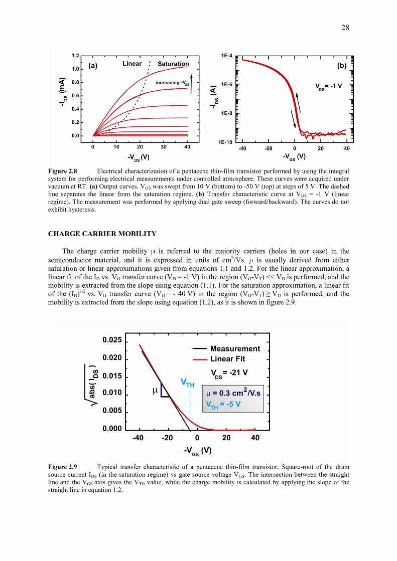
28
Figure 2.8 Electrical characterization of a pentacene thin-film transistor performed by using the integral
system for performing electrical measurements under controlled atmosphere. These curves were acquired under
vacuum at RT. (a) Output curves. VGS was swept from 10 V (bottom) to -50 V (top) at steps of 5 V. The dashed
line separates the linear from the saturation regime. (b) Transfer characteristic curve at VDS = -1 V (linear
regime). The measurement was performed by applying dual gate sweep (forward/backward). The curves do not
exhibit hysteresis.
CHARGE CARRIER MOBILITY
The charge carrier mobility is referred to the majority carriers (holes in our case) in the
semiconductor material, and it is expressed in units of cm2/Vs. is usually derived from either
saturation or linear approximations given from equations 1.1 and 1.2. For the linear approximation, a
linear fit of the ID vs. VG transfer curve (VD = -1 V) in the region (VG-VT) << VD is performed, and the
mobility is extracted from the slope using equation (1.1). For the saturation approximation, a linear fit
of the (ID)1/2
vs. VG transfer curve (VD = - 40 V) in the region (VG-VT) ≥ VD is performed, and the
mobility is extracted from the slope using equation (1.2), as it is shown in figure 2.9.
Figure 2.9 Typical transfer characteristic of a pentacene thin-film transistor. Square-root of the drain
source current IDS (in the saturation regime) vs gate source voltage VGS. The intersection between the straight
line and the VGS axis gives the VTH value, while the charge mobility is calculated by applying the slope of the
straight line in equation 1.2.

29
THRESHOLD VOLTAGE
The threshold voltage is defined as the gate voltage at which the device turns on, i.e. the onset of
accumulation. More correctly, the experimental VT is the value in the transfer curve that divides the
above-threshold regime (linear or saturation) from the sub-threshold regime. The value is obtained
from the intersection of the linear fit in the plot (IDS-1/2
vs. VGS) with the gate voltage axis (figure 2.9).
SUBTHRESHOLD SLOPE, ON/OFF RATIO AND PINCH-OFF VOLTAGE
The subthreshold slope is extracted at the steepest point in the plot of log(IDS) vs VGS (figure
2.10) It is reported in mV/decade, i.e. mV of VGS for every decade of IDS modulation. Smaller values
in these units correspond to a larger slope, which is in general the most desirable.
The ON/OFF ratio is the maximum (on) IDS value divided by the minimum (off) IDS value,
obtained from a transfer (IDS vs. VGS) measurement. This ratio characterizes the ability of the device to
switch the semiconductor channel on and off. We note that the (off) IDS must be greater than the
minimum current the instrument can measure, in order to be determined. Otherwise, the measure will
show the internal noise or dark current. Stray capacitances and parasitic effects can also corrupt the
measurement. These phenomena can be present in our case, since measured dark current is ~10 pA,
pentacene ultra-thin-films in their off region can have very low conductivity. So, the extracted on/off
ratio must be considered as the lower limit, and its value at the present can be even greater.
The intersection between the fitted straight line and the VGS axis in figure 2.10 gives the pinch-
off voltage that is the voltage at which the transistor turns on. Like the ON/OFF ratio, the extracted
VPinch-Off value depends on the minimum measurable current. Even if this value does not have a
physical definition, VPinch-Off together with the threshold voltage VTH give practical information about
the extension of the subthreshold regime.
Figure 2.10 Typical transfer characteristic of a pentacene thin-film transistor. Drain source current IDS in
log scale vs gate source voltage VGS in linear scale. The subthreshold slope, the pinch-off voltage and the
ON/OFF ratio are shown.
2.5 EXPERIMENTAL RESULTS
Here, we show a series of experiments performed in order to characterize pentacene TFTs by
applying the techniques above described. In addition, we present an innovative technique for
correcting the disturbing effects produced by the leakage current, which is very useful for extracting
the real electrical parameters.

30
2.5.1 ELECTRICAL PERFORMANCE OF TYPICAL PENTACENE TFTs
A set of 16 devices was fabricated under the same nominal conditions. The devices have a
channel length (L) of 20 and 40 m and width (W) of 11200 and 22400 m, respectively. Pentacene
was thermally sublimed at room temperature under HV (base pressure 1.10-7
mbar). The deposition
rate used was 2.5 ML/min and the final nominal thickness was 15 nm. Subsequently, all devices were
electrically characterized under vacuum ( 10-4
mbar). It is important to mention that all the samples
were treated before deposition, following the same cleaning protocol. Although, the cleaning
treatment will be explained in details in chapter 3, we need to remind that the nature of the surface
(e.g. roughness and clean conditions) is crucial for obtaining the same growth mode and reproducible
electrical performance. Typical output and transfer characteristic curves of pentacene thin-film
transistors are shown in figure 2.11(a) and (b), respectively.
Figure 2.11 Typical electrical characteristics of pentacene thin-film transistors with L = 40 m and
W = 22.4 mm. (a) Output curves. The VGS was swept from 10 V (bottom) to -40 V (top) at steps of 5 V.
(b) Transfer characteristic curves in linear (VDS = -1 V) and saturation regime (VDS = -40 V).
A non-ohmic contact response is slightly visible from the output characteristics in figure 2.11(a).
Its origin lies in the electronic structure [32], the structural and morphological disorder of the
organic/metal interface [6,33]. The hysteresis is due to exposition to ambient conditions before the
electrical characterization. In contact to the ambient, the sample can be affected by several elements,
such as humidity or oxygen [34,35].
The OTFT parameters above introduced, were extracted for each transfer characteristic curve in
linear and saturation regime. The mean value and the standard deviation are shown in Table 2.1. From
the table 2.1, we can noticed that the pentacene TFTs show comparable linear and saturation charge
mobilities around 0.1-0.2 cm2/V.s, which are close to the highest values reported in literature for
bottom contact pentacene devices on bare SiO2 surface [36]. The mobility is well reproduced from
sample to sample. High ON/OFF ratios are also obtained. The threshold voltages are near zero and
pinch-off voltages are positive. Both, threshold voltage and pinch-off voltage show a higher
dispersion with respect to mobility, due to sample to sample variations, but this is completely in
agreement with literature.
(a)
(b)

31
Linear regime (VD = -1 V)
(cm2/Vs)
VTH
(V) VPinch-Off
(V) ION/IOFF
Subthreshold
Slope (V/dec)
Mean 0.12 4.0 13.8 5×10⁵
1.46
Std. dev 0.05 3.2 4.4 - 0.63
Saturation regime (VD = -40 V)
(cm2/Vs)
VTH
(V)
VPinch-Off
(V) ION/IOFF
Subthreshold
Slope (V/dec)
Mean 0.18 0.4 18.6 4×10⁷ 1.48
Std. dev 0.05 3.4 7.8 - 0.69
Table 2.1 Electrical parameters extracted from 16 pentacene thin-film transistors grown at the same
conditions: 15 nm, 2.5 ML/min at room temperature.
2.5.2 CHANNEL LENGTH EFFECTS ON THE ELECTRICAL RESPONSE
The electrical behaviour of the OTFT can substantially differ when the channel length varies.
This can be easily observed from the output characteristics shown in figure 2.12. For L = 2.5 m it
can be seen that the drain current no longer saturates for high gate voltages. This behaviour may
suggest the presence of short channel effects, even though L is much larger than the dielectric
thickness (dSiO2 ~ 230 nm).
Figure 2.12 Measured output curves for various channel length (L); the gate voltage was swept in between
10 V and -50 V at steps of 5 V.

32
The charge carrier mobility and the threshold voltage were investigated as a function of channel
length. An analysis of the transfer curves shows a systematic shift of the threshold voltage with the
channel length. The threshold voltage shows a 1/L dependence (figure 2.13a). This behaviour is
typically observed when short channel effects are manifested. For the same L, comparable values of
charge mobility are obtained in both kinds of substrate as shown in figure 2.13(b). The pentacene
TFTs were grown under the same conditions, which shows the good reproducibility of our devices.
Figure 2.13 (a) Threshold voltage; and (b) charge mobility measured in linear regime, as a function of the
channel length L.
2.6 GATE LEAKAGE EFFECTS: A CORRECTING TECHNIQUE
Gate Leakage IG ideally is zero, at all bias conditions. Several different factors can lead to gate
leakage, affecting the performance of many circuits. Some of the most important factors are [37]:
(i) Inhomogeneities of the dielectric thickness.
(ii) Dielectric stress induced by prolonged exposure time to high electric field.
(iii) Mechanical damage of the dielectric layer.
(iv) Poor isolation between the organic layer and the gate. This point is usually resolved
by adding a mask on the substrate, which leaves the active channel area free but
covering the rest (especially over the edges) during the organic thin-film growth.
Figure 2.14 Schematic of an organic thin-film transistor. Two currents are monitored during the electrical
characterization, ID and IG.
(a) (b)

33
Since leakage current is not always avoidable, a simple correcting technique was developed and
it is explained below.
From figure 2.14, the conservation of charge requires that:
ID + IS + IG = 0 (2.1)
where ID, IS and IG are the effective current that flows in the drain, source and gate, respectively.
During the electrical characterization two currents are monitored, drain current ID and gate current IG.
IG = IGS + IGD (2.2) and ID = IDS - IGD (2.3)
The current in which we are interested is the channel current, i.e. drain source current IDS. By
combining equations (2.9):
IDS = ID + IG -IGS (2.4)
If VD = 0, then IDS = 0 and, by considering a symmetrical OTFT architecture, IG is divided in two
identical parts, IGD and IGS. In this case:
IGS (VD = 0) = IG + ID (2.5)
Since VS = 0 in all cases, we assume IGS given by eq. (2.12). If VD ≠ 0, drain source current is:
IDS = ID + IG – IGS (VD = 0) (2.6)
In conclusion, the drain source current is the sum of both values measured through the ammeters,
when a voltage is applied to the drain contact, less the sum of these measurements carried out when
the VD = 0.
We can apply this correction on a normal transfer characteristic curve of a typical pentacene
TFT. In figure 2.15(a) the contributions given by the drain current and by the leakage current are
compared. In figure 2.15(b) the method above explained was applied. Moreover, when the
measurement curve became anomalous because the leakage current effects (figure 2.16a), it is
possible to apply this correcting method for reconstructing the values (figure 2.16b).
Figure 2.15 Transfer characteristic curves of a pentacene thin-film transistor: (a) drain source current IDS
(red dots) and leakage current IG (black squares); (b) IDS (black squares) and its correction (red dots). It is
evident the usefulness of our correcting method, even in this case where the leakage current effects are not so
visible on the transfer characteristic.

34
Figure 2.16 Drain source current IDS of a pentacene thin-film transistor which presents a high leakage
current IG which hampers the measurements. (a) Direct measurement; and (b) measurement corrected by the
method explained above.
2.7 CONCLUSIONS
Pentacene TFTs have been fabricated and electrically characterized. The device performance is
strongly dependent on the growth parameters and the environmental conditions. In order to reach a
good reproducibility, the growth conditions and the environmental conditions were controlled.
The observation of hysteresis is due to the exposition to the ambient, where humidity or oxygen
can affect the final performance, so the electrical measurements were carried out under high vacuum.
The leakage current and the environmental conditions were monitored during the electrical
characterization to assure the stability performance. With the purpose of comparing the device
performance with those values reported in literature, standard procedures were applied during the
electrical parameters extraction.
Good enough reproducibility was reached, since growth parameters and environmental
conditions can be controlled under an acceptable range of variability. The electrical performance
exhibited by the fabricated devices is comparable to those reported in literature.
REFERENCES
[1] J. A. Venables, G. D. T. Spiller, and M. Hanbücken, Rep. Prog. Phys. 47, 399 (1984).
[2] A. Hoshino et al., J. of Crystal Growth 115, 826 (1991).
[3] D. E. Hooks, T. Fritz and M. D. Ward, Advanced Materials 13, 227 (2001).
[4] D. Käfer, L. Ruppel, and G. Witte, Phys. Rev. B 75, 085309 (2007).
[5] R. Ruiz et al., Phys. Rev. B 67, 125406 (2003).
[6] P. Stoliar et al., J. Am. Chem. Soc. 129, 6477 (2007).
[7] S Kowarik, A Gerlach, and F Schreiber, J. Phys.: Condens. Matter 20, 184005 (2008).
[8] F. Schreiber, Phys. Stat. Sol (a) 201, 1037 (2004).
[9] R. Lin et al., J. Chem. Phys. 117, 321 (2002).
[10] S. R. Forrest, Chem. Rev. 97, 1793 (1997). [11] C. D. Dimitrakopoulos, P. R. L. Malenfant, Adv. Mater. 14, 99 (2002).
[12] R. Ruiz et al., Phys. Rev. Lett. 91, 136102 (2003).
[13] F.-J. Meyer zu Heringdorf, M. C. Reuter, R. M. Tromp, Nature 412, 517 (2001).
[14] R. B. Campbell, J. M. Roberston, J. Trotter, Acta Crystallogr. 15, 289 (1962).
[15] D. Holmes et al., Chem. Eur. J. 5, 3399 (1999).

35
[16] T. Siegrist et al., Angew. Chem., Int. Ed. 40, 1732 (2001).
[17] E. Venuti et al., J. Am. Chem. Soc. 124, 2128 (2002).
[18] M. Shtein et al., App. Phys. Lett. 81, 268 (2002).
[19] M. Brinkmann, S. Pratontep, C. Contal, Surf. Sci. 600, 4712 (2006).
[20] B. Nickel et al., Phys. Rev. B 70, 125401 (2004).
[21] A. Shehu, S. D. Quiroga, P. D’Angelo, C. Albonetti, F. Borgatti, M. Murgia, A. Scorzoni, P.
Stoliar, F. Biscarini, submitted (2010).
[22] S. Pratontep et al., Phys. Rev. B 69, 165201 (2004).
[23] S. Pratontep et al., Synth. Met. 146, 387 (2004).
[24] S. Verlaak et al., Phys. Rev. B 68, 195409 (2003).
[25] S. Hong et al., App. Phys. Lett. 92, 253304 (2008).
[26] R. Ruiz et al., Chem Mater. 16, 4497 (2004).
[27] A. C. Mayer et al., Org. Electr. 5, 257 (2004).
[28] F. Borgatti et al., unpublished results (2010).
[29] F. Dinelli et al., Phys. Rev. Lett. 92, 116802 (2004).
[30] J.-F. Moulin et al., N. Ins. and Met. in Phys. Res. B 246, 122 (2006).
[31] F. Gutmann, L. E. Lyon, E. Rob’t. Krieger Publishing: Malabar, FL, 1981.
[32] F. Amy, C. Chan, A. Kahn, Org. Elect. 6, 85 (2005).
[33] K. Asadi et al., Adv. Mater. 21, 1 (2009).
[34] H. L. Gomes et al., Journal of Non-Crystalline Solids 352, 1761 (2006).
[35] Y. Hu et al., J. Phys. D: Appl. Phys. 39, 4553 (2006).
[36] S. Kobayashi et al., Nature Mat. 3, 317 (2004).
[37] A. Hoppe et al., Phys. Stat. Sol. (a) 205, 612 (2008).

36

37
This chapter is focused on the experimental setup and the different methods employed for
performing the electrical and morphological characterization of organic ultra-thin-film transistors.
After a brief introduction of these techniques, we describe the layout of our samples, the cleaning
treatment and the approach that we have chosen to investigate organic electronic devices under real
operating conditions. A full description of our experimental setup and representative results are
shown.
3.1 INTRODUCTION
Real-time and in situ techniques are promising tools for studying dynamic phenomena such as
growth of thin-films and nanostructures. Real-time experiments access the finer details of the growth
kinetics, for instance nucleation and the early stages of growth, which are difficult to resolve by ex-
situ experiments [1]. In situ monitoring of material properties guarantees the same environmental
conditions along the whole duration of the experiment [2] and thus prevents these measurements from
being affected by structural relaxation and reorganization, or parasitic effects due to the interaction
with environmental agents (water, oxygen or light) which interfere with or overlap to the intrinsic
response of the material [3,4]. The combination of both methods is powerful especially for studying
the physics of low-dimensional devices formed by self-organization or other bottom-up process. It
allows one to map the relevant parameter space, yielding longer operational lifetime and a low-cost
device technology [5].
Investigations in real-time and in situ of organic semiconductors on a variety of models and
technological substrates by He-atom scattering [6,7], low-energy electron microscopy [8], X-ray
scattering [9-12] have shown a direct correlation between morphological and structural parameters
and the growth mode. Other experiments showed correlations between electrical properties and
growth parameters but did not explore the morphology and the structure of the growing film [13-15].
It is important to experimentally address the correlation between the OTFT electrical response and the
morphological and structural changes that take place during the growth of the thin-film [16].
These experiments require a high sensitivity of the measurements, spanning several orders of
magnitude of the observable; suitable time resolution and stable environmental parameters for the
control of the growth mode. The combination of real-time and in situ techniques represents a powerful
tool that allows us to carry out electrical monitoring on operating devices under real working
conditions. Among the most important advantages, the changes on the electrical response can be
directly correlated to the instant film thickness [17], which is an important parameter controlling the
film morphology. In fact, the morphology is a scaling property of the film thickness and the
deposition rate.
In this chapter we describe a home-designed and home-built experimental setup consisting of a
thermal sublimation system that allows us to carry out a complete electrical investigation of organic
ultra-thin-films in real time during their growth on test field-effect transistor structures; after growth,
the devices can be further characterized in situ keeping the environmental parameters unchanged with
the initial conditions. Our system, being an open equipment with a flexible design that supports

38
several mounting configurations, allows us to explore a variety of devices, organic materials and
experimental parameters, just changing a few elements of the setup. Furthermore, the system is
portable and could be readily adapted for x-ray experiments at synchrotron beamlines.
3.2 SAMPLES ARCHITECTURE
In the experiments presented here, we have used two kinds of substrate, schematically shown in
figure 3.1. The first substrate was supplied by Fondazione Bruno Kessler from Trento, Italy (termed
FBK), while the second substrate was commercially supplied by Fraunhofer Institut Photonische
Mikrosysteme from Dresden, Germany (termed Fraunhofer). These substrates are termed test
patterns. In both cases, highly n-type doped Si (100) wafer was used as substrate and as common gate
in a bottom contact configuration. In the FBK substrate the resistivity is 0.01-0.03 cm; whilst in
Fraunhofer substrate the resistivity is 1.5-3.0 cm. We employed high-quality 150 mm Si wafers
according to the standard (675 ± 40 μm thickness).
In the FBK the gate dielectric layer was formed with 200 nm of thermally grown SiO2 with a
capacitance of 17.25x10⁻⁹
F/cm2. An adhesive layer of Cr (3-5nm) was patterned before the gold
electrodes with a final thickness around 150 nm were deposited by lift-off technique. The Au contacts
which act as source (S) and drain (D) exhibit interdigitated geometry with channel length (L) of 20
and 40 m and width (W) of 11200 and 22400 m, respectively. In the Fraunhofer substrate the gate
dielectric layer consisted of 230 nm of thermally grown SiO2 with a capacitance of 15.10-9
F/cm2. The
adhesion layer was made of ITO (Indium Tin Oxide) with a thickness of 10 nm using lift-off. ITO is a
solid solution of indium(III) oxide (In2O3) and tin(IV) oxide (SnO2), typically 90% In2O3 and 10%
SnO2 by weight. In this case, the Au contact pads or electrodes were deposited with a final thickness
of 30 nm and exhibit interdigitated geometry with four different values of the channel length (L)
ranging between 2.7 m and 20 m, and a fixed width (W) of 10 mm.
Figure 3.1 Schematics of the two test bed device architecture employed in our experiments, with
pentacene on top. All the materials were the same, except for the adhesion layer: Cr for the FBK substrate and
ITO for the Fraunhofer substrate.
The FBK substrate has four transistors divided in two different geometries, while the Fraunhofer
substrate presents 16 transistors divided in four series of four transistors each one, with the same
geometrical characteristics. In figure 3.2 it can be seen the surface scheme of both kinds of substrate,
exhibiting the interdigitated gold electrodes. The FBK substrate presents larger gold contacts or pads
and thicker gold layer that make possible an easier handling during the preparation for real-time and
in situ electrical monitoring, especially for wire bonding. The Fraunhofer substrate presents a higher
number of samples which is useful to improve the statistics. All the transistors have a fixed channel
width W and four different channel lengths L, allowing us to assess the contact resistance, for
example through the transmission line method (TLM) [18,19].

39
Figure 3.2 Test Patterns Scheme of: (a) FBK substrate (10 mm x 10 mm), and (b) Fraunhofer substrate
(15 mm x 15 mm). (c) One transistor of the Fraunhofer substrate, where source, drain and the active channel are
indicated (the detail shows the interdigitated structure present in this area).
3.3 SAMPLE CLEANING TREATMENT
The FBK substrate presents an initial roughness (RMS) value between 0.8 nm, in the best
situation and, occasionally, in excess of 4 nm. The latter values measured by AFM reveal the presence
of organic and inorganic residues remaining from the fabrication. In this respect, the lift-off, a
procedure present during the production, gives an additional problem related to the charge carrier
injection. After the Cr adhesive layer is deposited on the SiO2, the Au deposition is followed by using
lift-off technique. Au deposit cannot fully cover the Cr beneath. When the organic semiconductor is
subsequently deposited, the first monolayers of it are in contact with the Cr instead to be in contact
with the Au layer, changing the labor function (figure 3.3a). Consequently, the whole electronic
response of the device decreases significantly.
Williams et al. [20,21] have experimentally found the etching rates of photoresist, organic, Au,
Cr, SiO2 and Si in contact with acetone, Piranha and HF. These etch rates are shown in Table 3.1:
Thin Film/Substrates
Etchant PR ORG Au Cr SiO2 Si
Acetone F F 0 S 0 S
Piranha (1:50 H2O2:H2SO4) at 120°C F F 0 >16 0 0
HF (1:25 HF:milliQ H2O2) at RT 0 0 S 0 2.3-9.7 S (Notation: PR = Photoresist. ORG = Organic. F = fast, but not measured. S = slow or zero, but not
measured).
Table 3.1 Etching rates (nm/min) of different materials present in our samples when they are in contact
with acetone, Piranha solution and HF [20,21].
According to this information, we can remove the organic/inorganic residues as well as the
excess Cr layer by immersing FBK substrate in hot Piranha solution (1:1 H2O2:H2SO4) for 15 min.
Piranha solution attacks the organic residues present on the surface, reducing the roughness. This
roughness decrease determines an adequate growth mode and avoids inhomogeneities on the
pentacene ultra-thin-film. Also, part of the Cr adhesive layer is attacked by hot Piranha solution,
producing the migration and collapse of the Au layer. The physical changes that take place during and
immediately after hot Piranha treatment are schematically shown in figure 3.3(b-c). Once the
pentacene deposition is carried out, the organic semiconductor forms a direct contact with Au. Finally,
in order to reach the smaller possible roughness, the substrate was put in a HF solution (2:100
HF:H2O) at room temperature for a few seconds. The sample was rinsed with milliQ water and dried

40
with N2 at the end of every bath. Finally, the samples were exposed to acetone vapors for
approximately 1 min.
In the case of the Fraunhofer substrate it is not possible to apply the cleaning treatment explained
above, for smoothing the surface roughness. In fact ITO is completely attacked by hot Piranha
solution, which does not allow a good control of this procedure. At the end of this treatment, the Au
layer looses the whole adhesive layer and then, and all the material present on the surface is dissolved
into the solution. Fortunately, the Fraunhofer substrate exhibits a smaller roughness (< 0.5 nm) and it
is not necessary to adopt this cleaning protocol for obtaining a good control on the growth mode.
However, this substrate has the same problem regarding the electronic injection that it is present on
the FBK substrate. The first monolayers of pentacene are in contact with the ITO adhesion layer
instead to be in contact with the Au layer. Since in this case, hot Piranha treatment is not feasible
technique, we need to apply an alternative method such as plasma.
Figure 3.3 Scheme of a typical FBK substrate: (a) after deposition without cleaning treatment, where the
electronic injection is carried out through the Cr adhesion layer; (b) during the hot Piranha treatment, where it
can be seen the Cr attack that produces the Au layer migration and its collapse; (c) after hot Piranha treatment.
Pentacene is put directly in contact with the Au layer, improving the charge carrier injection and, consequently,
the whole electrical response.
3.4 EXPERIMENTAL SETUP: THE REAL-TIME AND IN SITU GROWTH SYSTEM
The main goal of this thesis was to find a correlation for OTFTs between growth parameters,
electrical properties and morphology. On this purpose, it was necessary to develop a special system
for performing a real-time and in situ electrical monitoring of OTFTs. In this section, we present the
most relevant details of this experimental setup: design, construction, mounting, calibration and
operation. All the parts of this system were entirely designed, developed and assembled at the CNR-
ISMN laboratories.
In this section we present a home-built experimental setup consisting of a thermal sublimation
system that allows us to carry out a complete electrical investigation of organic ultra-thin-films in
real-time during their growth on test field-effect transistor structures; after growth, the devices can be
characterized in situ keeping the environmental parameters unchanged with the initial conditions. Our
system, being an open equipment with a flexible design that supports several mounting
configurations, allows us to explore a variety of devices, organic materials and experimental
parameters, just changing a few elements of the setup. Furthermore, the system is portable and could
be readily adapted for X-ray experiments at synchrotron beam-lines.
3.4.1 HIGH VACUUM CHAMBER AND SAMPLE-HOLDER
Our system is shown in figure 3.4(a), where the main elements have been tagged. It is composed
of heater sample-holder, shutter (1), two independent high vacuum (HV) chambers (2,4) connected
through a pneumatic gate valve (7), quartz crystal microbalance (3), external electrical connections to

41
the instruments (5), shutter (6) and Knudsen cell (8). The pneumatic gate valve separates the HV
upper chamber, where the sample is placed, from the lower HV chamber, where the organic material
is stored inside the Knudsen cell. Both chambers are pumped independently. The double HV chamber
makes possible opening the upper chamber for changing the sample several times without putting the
organic material in contact with air. As consequence of this the contamination introduced into the
system and the pumping time of the upper HV chamber before deposition were significantly reduced.
Once the organic semiconductor is outgassed it can be kept cleaner for subsequent growth, thus
decreasing the fluctuations of the growth conditions or the physical-chemical changes of the
semiconductor, such as oxidation. Figure 3.4(b-c) shows the sample-holder dismounted in two parts
(1a and 1b) and re-mounted, respectively. Since the sample-holder can be detached from the rest of
the system, it is possible to make all the electrical connection between source and drain contact pads
on top of the substrate and the Au contacts on top of the sample-holder by ball- or wedge- bonding
technique.
The interior of our system is schematically shown in figure 3.5. The Knudsen cell (8) contains a
heating W wire (9) shrouding a fused quartz crucible (10) where organic material is placed. The
substrate temperature and the Knudsen cell temperature are regulated through PID microprocessor-
based controller with a precision of ± 1 °C. The shutter protects the sample from the subliming
organic semiconductor. When the desired deposition rate is reached and its value is constant the
shutter is removed and the growth starts.
Figure 3.4 (a) Front view of the home-built experimental setup for performing real-time and in situ
electrical monitoring. The main elements have been tagged: (1): sample-holder; (2): upper HV chamber; (3):
quartz crystal microbalance; (4): lower HV chamber; (5): external electrical connections (to the instruments),
(6): shutter; (7): pneumatic gate valve; (8): Knudsen cell. (b) View of the sample-holder dismounted in two
parts (1a, 1b) for allowing the use of the bonding technique between the substrate and the contacts placed on the
sample-holder; and (c) the sample-holder once it is mounted, after the bonding technique was applied.

42
Figure 3.5 Schematic cross section of the system showing the main elements: (1): sample-holder; (2):
upper HV chamber; (3): quartz crystal microbalance; (4): lower HV chamber; (5): external electrical
connections (to the instruments), (6): shutter; (7): pneumatic gate valve; (8): Knudsen cell, composed of (9): a
heating Tungsten wire and (10): the crucible containing the pentacene. Inset: detail of the sample-holder
showing: (11): feedthrough; (12): transistor; (13): source and drain (S/D) Au contact pad on the substrate; (14):
Au contact pad on the sample holder; (15): bonding; (16): the bottom of the test pattern substrate which acts as
common gate (G).
The inset on figure 3.5 is shown enlarged with its corresponding optical microscope image on
figure 3.6, where the Au contact pads and the bonding are indicated. In this case wedge bonding was
applied, allowing the electrical conduction between source or drain on top of the substrate and the Au
contact on top of the sample-holder. The bottom of the substrate acts as common gate and the sample
is placed on top of the sample-holder by using silver paste to assure a better electrical conduction
between the gate and the corresponding contact on the sample holder. Every Au contact pad on top of
the sample-holder is electrically connected to the external instruments outside the HV chamber by
feedthroughs.
The top of the sample-holder is made of Shapal, a ceramic which is an excellent electrical
insulator with a high thermal conductivity. This material was chosen because it allows a reliable
estimate of the substrate temperature, which is measured by an embedded thermocouple, and avoids
shortcuts between different parts in contact with the top of the sample-holder. The substrate
temperature can be raised up to 250°C. A special rigid mask covers the contacts on the substrate and
on the sample-holder leaving free the OTFT active channel area for deposition, thus reducing the
number of parasite currents and the probability of shortcuts between top and bottom of the substrate.
The film thickness (expressed in monolayers, ML) is monitored by a quartz crystal microbalance
previously calibrated using atomic force microscopy (AFM) measurements in sub-monolayer thick
film. The typical base pressure for our HV system is 2.10-6
mbar.

43
Figure 3.6 Schematic detail of the sample-holder (left) and an optical microscopy image of this part of
the system (right), where the main elements have been indicated. The bonding allows the electrical connection
between the Au contact pads on the substrate and the Au contacts on top of the sample-holder.
3.4.2 ELECTRICAL CONNECTIONS AND SOFTWARE
A simplified scheme with the main electrical connections present in this system is shown in
figure 3.7. The electrical measurements were performed using two electrometers: Keithley 6430 and
2612. The first one was employed for setting VGS and for monitoring IGS. The second electrometer,
being a double channel, was used for setting and monitoring VDS and IDS respectively on both
transistors. The synchronization between themselves and with the PC was established through a
GPIB/USB data bus.
Figure 3.7 Simplified electrical scheme exhibiting the main connections present on our system. The HV
chamber (dashed closed line) contains both transistors that can be electrically monitored during deposition. The
information flow direction is indicated by gray arrows.

44
To decrease the electrical noise present during measurements, every contact on the sample-holder
was electrically connected to the external instruments through individual biaxial-cables using special
connectors for vacuum. All these connections are independent each other to prevent electrical
crosstalk, especially when one of those present a relevant leakage current. The leakage current usually
appears when there is an electrical path between the bottom of the substrate (common gate) and
source/drain contact on top. In this case the IG can be increased several orders of magnitude,
producing spikes or other kind of instabilities on the measurements. By avoiding the leakage currents
or their influence as much as possible the measurements exhibit a smooth behavior and reflect more
accurately the contributions emerging during growth.
Figure 3.8 Visual interface of our personalized software, composed of: (a) program used for performing
real-time electrical monitoring and post-growth in situ electrical characterization, and (b) program for
monitoring the quartz crystal microbalance.
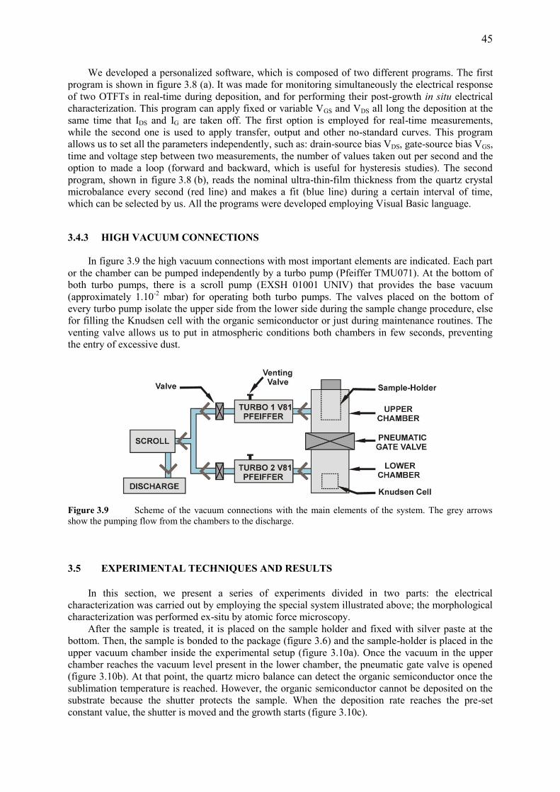
45
We developed a personalized software, which is composed of two different programs. The first
program is shown in figure 3.8 (a). It was made for monitoring simultaneously the electrical response
of two OTFTs in real-time during deposition, and for performing their post-growth in situ electrical
characterization. This program can apply fixed or variable VGS and VDS all long the deposition at the
same time that IDS and IG are taken off. The first option is employed for real-time measurements,
while the second one is used to apply transfer, output and other no-standard curves. This program
allows us to set all the parameters independently, such as: drain-source bias VDS, gate-source bias VGS,
time and voltage step between two measurements, the number of values taken out per second and the
option to made a loop (forward and backward, which is useful for hysteresis studies). The second
program, shown in figure 3.8 (b), reads the nominal ultra-thin-film thickness from the quartz crystal
microbalance every second (red line) and makes a fit (blue line) during a certain interval of time,
which can be selected by us. All the programs were developed employing Visual Basic language.
3.4.3 HIGH VACUUM CONNECTIONS
In figure 3.9 the high vacuum connections with most important elements are indicated. Each part
or the chamber can be pumped independently by a turbo pump (Pfeiffer TMU071). At the bottom of
both turbo pumps, there is a scroll pump (EXSH 01001 UNIV) that provides the base vacuum
(approximately 1.10-2
mbar) for operating both turbo pumps. The valves placed on the bottom of
every turbo pump isolate the upper side from the lower side during the sample change procedure, else
for filling the Knudsen cell with the organic semiconductor or just during maintenance routines. The
venting valve allows us to put in atmospheric conditions both chambers in few seconds, preventing
the entry of excessive dust.
Figure 3.9 Scheme of the vacuum connections with the main elements of the system. The grey arrows
show the pumping flow from the chambers to the discharge.
3.5 EXPERIMENTAL TECHNIQUES AND RESULTS
In this section, we present a series of experiments divided in two parts: the electrical
characterization was carried out by employing the special system illustrated above; the morphological
characterization was performed ex-situ by atomic force microscopy.
After the sample is treated, it is placed on the sample holder and fixed with silver paste at the
bottom. Then, the sample is bonded to the package (figure 3.6) and the sample-holder is placed in the
upper vacuum chamber inside the experimental setup (figure 3.10a). Once the vacuum in the upper
chamber reaches the vacuum level present in the lower chamber, the pneumatic gate valve is opened
(figure 3.10b). At that point, the quartz micro balance can detect the organic semiconductor once the
sublimation temperature is reached. However, the organic semiconductor cannot be deposited on the
substrate because the shutter protects the sample. When the deposition rate reaches the pre-set
constant value, the shutter is moved and the growth starts (figure 3.10c).
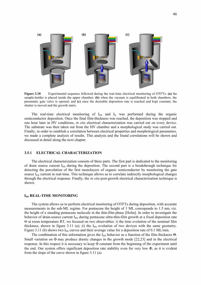
46
Figure 3.10 Experimental sequence followed during the real-time electrical monitoring of OTFTs: (a) the
sample-holder is placed inside the upper chamber; (b) when the vacuum is equilibrated in both chambers, the
pneumatic gate valve is opened; and (c) once the desirable deposition rate is reached and kept constant, the
shutter is moved and the growth starts.
The real-time electrical monitoring of IDS and IG was performed during the organic
semiconductor deposition. Once the final film-thickness was reached, the deposition was stopped and
one hour later in HV conditions, in situ electrical characterization was carried out on every device.
The substrate was then taken out from the HV chamber and a morphological study was carried out.
Finally, in order to establish a correlation between electrical properties and morphological parameters,
we made a complete analysis of results. This analysis and the found correlations will be shown and
discussed in detail along the next chapter.
3.5.1 ELECTRICAL CHARACTERIZATION
The electrical characterization consists of three parts. The first part is dedicated to the monitoring
of drain source current IDS during the deposition. The second part is a breakthrough technique for
detecting the percolation of the first monolayers of organic semiconductor by monitoring the gate
source IGS current in real-time. This technique allows us to correlate indirectly morphological changes
through the electrical response. Finally, the in situ post-growth electrical characterization technique is
shown.
IDS REAL-TIME MONITORING
The system allows us to perform electrical monitoring of OTFTs during deposition, with accurate
measurements in the sub-ML regime. For pentacene the height of 1 ML corresponds to 1.5 nm, viz.
the height of a standing pentacene molecule in the thin-film phase [Holm]. In order to investigate the
behavior of drain-source current IDS during pentacene ultra-thin-film growth at a fixed deposition rate
at room temperature RT, we focused on two observables: i) the time evolution of the nominal film
thickness, shown in figure 3.11 (a); ii) the IDS evolution of two devices with the same geometry.
Figure 3.11 (b) shows two IDS curves and their average value for a deposition rate of 0.1 ML/min.
The combination of this information gives the IDS behavior as a function of the film thickness .
Small variation on may produce drastic changes in the growth mode [22,23] and in the electrical
response. In this respect it is necessary to keep constant from the beginning of the experiment until
the end. Our system offers significant deposition rate stability even for very low , as it is evident
from the slope of the curve shown in figure 3.11 (a).

47
Since organic ultra-thin film growth by sublimation is a non-equilibrium phenomenon [17], the
possibility to measure simultaneously two transistors in real-time is an important advantage of this
system. In this way growth and environmental conditions are the same for both samples, reducing the
necessary experimental time and improving the statistics. The latter point can be understood better by
observing figure 3.11 (b). At the light of other experiments that we are not presenting here, the
identical electrical response exhibited on both transistors reveals exactly the same growth mode. This
approach can be upscaled to many devices, to construct a robust statistics.
The results presented here were obtained by applying fixed gate-source bias VGS = -40 V and
drain-source bias VDS = -1 V along the experiment, while IDS was acquired every 200 ms. The
evaporation was stopped at a final nominal coverage of 7 ML. Another advantage of our setup is the
electrical independency of every connection that allows us to set individual VGS and VDS values for
each transistor. This feature makes possible to perform electrical monitoring of two devices under
different electrical configurations but with the same growth and environmental conditions, which is
required in studies related to electric-field effect on organic materials.
Figure 3.11 Real-time electrical monitoring. (a) Measurements obtained by the quartz crystal microbalance
showing the film thickness along the time. (b) Evolution of the electrical response of two ultra-thin-film
transistors measured simultaneously during deposition (solid black line) and their average curve (dash red line).
IG REAL-TIME MONITORING: A METHOD FOR OBSERVING THE PERCOLATION
THRESHOLD
Organic field-effect transistors usually exhibit an undesirable leakage current IG between
source/drain and gate, due to inhomogeneities on the oxide thickness that ease the electrical
breakdown. Sizable IG produces anomalies on the electrical response, such as spikes and other
detrimental effects on IDS. However, under certain range of values the IG can be used as an indicative
parameter of a transitory effect occurring during the organic material deposition. This is the case
when IG is at least one order of magnitude smaller than IDS. By monitoring IG in real-time it is possible
to determine the exact moment in which a particular phenomenon takes place, even when this event is
observable during a very short time only.

48
The test pattern structure presents a metal-insulator-metal (MIM) Si-SiO2-Au capacitor behavior,
with an initial capacitance of 1.725x10⁻⁸
F/cm2. Once the growth starts, the organic material thickness
increases, changing gradually the geometry of the structure, thus its capacitance. At the beginning IDS
is very low, generally below 10-10
A. When the percolation of the first ML occurs the capacitor
configuration suddenly changes, introducing a transitory effect which is made evident on the IG
response, according to Equation 3.1:
(3.1)
The parenthesis term is the MIM capacitance C, where is the dielectric permittivity, L and W
are the channel length and width; (t) is the coverage which is 0 at the beginning of deposition and its
value is 1 when one ML is completely deposited. Considering c as the nominal thickness at which
percolation occurs, if c then IG (t) = 0 because there is not a connected electrical path between
source and drain, therefore IDS cannot flow. When = c there is electrical conduction between
source and drain, thus a variation of C suddenly appears and IG ≠ 0.
Figure 3.12 Pentacene ultra-thin-film transistor grown with a deposition rate of 0.1 ML/min at room
temperature. Real-time evolution of: (a) drain/source current IDS; and (b) gate current IG. The AFM images show
a typical morphology present: (c) during the percolation of the first ML; (d) during the percolation of the second
ML; and, (e) at the end of deposition.
Real-time monitoring of IDS and its corresponding IG are shown in figure 3.12(a) and 3.12(b),
respectively. IG exhibits two peaks at 0.7 and 1.6 ML. Studies performed ex-situ by using the AFM
show the morphology present at different nominal film thicknesses, confirming that both IG peaks

49
correspond to the percolation of the first (figure 3.12c) and second (figure 3.12d) pentacene
monolayer, respectively. In figure 3.12(c) we clearly observe the SiO2 surface and small pentacene
islands in contact each other, while figure 3.12(d) shows an almost complete first ML (intermediate
color) with some regions where SiO2 is still exposed (black), the second ML islands (lighter color) are
just touching each other and there are also some nucleated and growing upper monolayer islands on
top. Finally, in figure 3.12(e) it is seen the typical dendritic morphology of pentacene grown on SiO2
at a final nominal film thickness of 7ML. The growth was performed employing a deposition rate of
0.1 ML/min at RT.
This is the first time that this electrical observation is reported to show that this method
represents a powerful tool for locating the percolation threshold of the first and the second ML of
organic semiconductors. It should be said that the percolation is strongly dependent of the growth
mode and could be observed with different features for other growth parameters. Another reason for
the impossibility of observing the percolation of upper ML is the fact that for thicker films the
penetration of the electric-field is reduced exponentially. The importance of this technique lies in the
fact that an electrical signal provides information about thin-film morphology, establishing a direct
correlation between both properties at the early stages of growth.
IN SITU POST-GROWTH ELECTRICAL CHARACTERIZATION
The in situ post-growth electrical characterization is carried out by applying transfer and output
curves under the same environmental conditions present during deposition, such as Tsubstrate, pressure
and absence of light. In this way charge transport properties probed after deposition are the intrinsic
one, which are related to order-disorder in ultra-thin-films (i.e. structural defects), not being affected
by external factors [24,25].
The output curves exhibit the contact resistance behavior and allow us to identify the linear and
saturation regimes of the organic field-effect transistor operations, while the transistor parameters are
obtained from transfer characteristic curves: charge mobility , threshold voltage VTH, maximum
drain-source current IDSmax and ION/IOFF ratio [26].
Figure 3.13 In Situ post-growth electrical characterization. Typical output curves (a) and transfer
characteristic curves (b) of a pentacene ultra-thin-film transistor. The first measurements were performed under
uninterrupted vacuum conditions (solid black line); finally, upon exposure to air, all the measurements were
repeated (dash red line). It is evident that hysteresis appears when the organic material is in air conditions only.
In figure 3.13(a) it is shown the typical output curves for an OTFT of pentacene, while in figure
3.13(b) we observe the corresponding transfer characteristic curves. In both cases the measurements
performed under vacuum are in solid black line while those performed in air are drawn as dashed red
line. By comparing the electrical responses, we notice no-hysteresis in the curves acquired under
vacuum, higher IDS and VTH closer to zero with respect to air [24]. These properties can be largely

50
modified by the exposure to air and they are usually irreversible as the device is stressed by the
repeated measurements. For this reason the in situ technique is a reliable and stable way to measure
their intrinsic values accurately.
The in situ technique is fundamental to study the inherent stability of the sublimed organic
material. It can be carry out by monitoring the electrical properties along the time from its deposition,
because under vacuum only the natural material degradation is present. Additionally, the system can
be modified to perform investigations under inert gas atmosphere by connecting an inert gas line to
the venting valve and introducing it inside the system instead of air when the vacuum condition is
broken.
3.5.2 MORPHOLOGICAL CHARACTERIZATION
After electrical characterization all the samples were taken out from the chamber for ex-situ
morphological investigation of the film with a Smena-A by NT-MDT AFM operated in non-contact
mode using Si tips (5.5-22.7 N/m and 190-325 kHz). AFM images of 512 X 512 points of resolution
were obtained by scanning areas between 5 m x 5 m and 20 m x 20 m. We calculated the
correlation length by using the power spectra density (PSD) function of the AFM topographical
profiles following analysis in ref. [27]. The correlation length is defined as:
(3.2)
where is the variable in the Fourier space. Figure 3.14(a) shows an AFM image and the practical
method employed by using the PSD function for obtaining the correlation length, in which the
intersection between two straight lines defines the value (figure 3.14 b). The correlation length is an
estimate of the mean distance between two adjacent islands and, in a 2D growth represents the mean
size of the islands.
In order to improve the statistics of our analysis, we have investigated at least three different
regions on the same sample for each device. We also compared the morphology present on the active
channel with the morphology far from the interdigitated gold contacts in order to verify that the
growth mode is the same all over the surface.
Figure 3.14 Pentacene on SiO2 grown employing a deposition rate of 0.1 ML/min at room temperature: (a)
AFM image, showing the typical morphology present in this kind of sample; and (b) the PSD function for the
previous AFM image, where and are numerically indicated.

51
3.6 CONCLUSIONS
The experimental setup introduced here combines real-time and in situ electrical monitoring
techniques resulting in a powerful tool to investigate dynamic phenomena in organic devices and
materials, from the beginning until the end of the growth process. This experimental setup has two
important characteristics: the flexibility which allows us to study a large number of parameters just
changing few components or settings; the possibility to examine two operating electronic devices at
the same time, which significantly improves the statistics of our results.
Additionally, we have shown the extraordinary potential of this system for obtaining the direct
correlation between the electrical and the morphological parameters through electrical real-time
monitoring [12]. This is a breakthrough feature of our system. We have demonstrated by the first time
a reliable correlation between the OTFT electrical response and the percolation of the organic
semiconductor.
The experiments presented in this article have not exhausted all the potentiality of this system
and there are more issues that can be investigated with it. Some possible studies on OTFTs in which
real-time and in situ techniques could be applied are: charge injection in functionalized gold contacts
[28]; electrical response under controlled atmosphere of gases [29], and impedance (LCR)
measurements [30].
REFERENCES
[1] A. Gerlach et al., Phys. Stat. Sol (a) 205, 461 (2008).
[2] G. Yoshikawa et al., Surface Science. 600, 2518 (2006). [3] H. L. Gomes et al., Journal of Non-Crystalline Solids 352, 1761 (2006).
[4] Y. Hu et al., J. Phys. D: Appl. Phys. 39, 4553 (2006).
[5] S. R. Forrest, Chem. Rev. 97, 1793 (1997).
[6] M. Buongiorno Nardelli et al., Phys. Rev. B 53, 1095 (1996).
[7] S. Prato et al., J. Phys. Chem. B 103, 7788 (1999).
[8] F.-J. Meyer zu Heringdorf, M. C. Reuter & R. M. Tromp, Nature 412, 517 (2001).
[9] A. C. Dürr et al., Phys. Rev. Lett. 90, 016104 (2003).
[10] A. C. Mayer et al., Organic Electronics 5, 257 (2004).
[11] J.-F. Moulin et al., Nuclear Instr. and Meth. in Phys. Res. B 246, 122 (2006).
[12] S. Milita et al, J. of Phys. Chem. C 112, 12177 (2008).
[13] T. Muck et al. Synth. Met. 146, 317 (2004).
[14] M. Kiguchi et al. Phys. Rev. B 71, 035332 (2005).
[15] B. N. Park, S. Seo and P. G. Evans, J. Phys. D: Appl. Phys. 40, 3506 (2007).
[16] A. Shehu, S. D. Quiroga, P. D’Angelo, C. Albonetti, F. Borgatti, M. Murgia, A. Scorzoni, P.
Stoliar, F. Biscarini, submitted (2010).
[17] S. Kowarik, A. Gerlach, F. Schreiber, J. Phys.: Condens. Matter 20, 184005 (2008).
[18] H. Klauk et al., Solid-State Electron. 47, 297 (2003).
[19] P. V. Necliudov et al., Solid-State Electron. 47, 259 (2003).
[20] Kirk R. Williams, and Richard S. Muller, J. of Microelectromechanical Systems 5, 256 (1996).
[21] Kirk R. Williams et al., J. of Microelectromechanical Systems 12, 761 (2003).
[22] Sirapat Pratontep et al., Physical Review B 69, 165201 (2004).
[23] Martin Brinkmann, Sirapat Pratontep, Christophe Contal, Surf. Science 600, 4712 (2006). [24] P. D’Angelo et al., Appl. Phys. A 95, 55 (2009) [25] Y.-W. Wanga et al., Thin Solid Films 467 (2004) 215– 219.
[26] Wolfgang Brütting, Physics of Organic Semiconductors, WILEY-VCH Verlag GmbH & Co
(Weinheim) Edition 2005.
[27] F. Biscarini et al., Phys. Rev. Lett. 78, 2389 (1997).
[28] P. Stoliar et al., J. Am. Chem. Soc. 129, 6477 (2007).
[29] W.Y. Chou et al., Organic Electronics 7, 445 (2006).
[30] B. H. Hamadani et al., Applied Physics Letters 92, 203303 (2008).

52

53
In this chapter we present a correlation for pentacene thin-film transistors between growth
conditions, electrical measurements performed in real-time and in situ, and morphology. Drain-source
current IDS in organic thin film transistors has been monitored during the deposition of pentacene. The
current increases below the first monolayer (ML), and saturates after 2 to 7 MLs of nominal thickness
depending on the deposition rate. The number of active layers, their individual contribution to the
current, and the spatial distribution of charge carriers are all modulated by the growth mode. The
effective Debye length of the organic semiconductor thin-film scales as the morphological correlation
length. Earlier controversial results are unified within this framework.
4.1 INTRODUCTION
Organic Thin-Film Transistors (OTFTs) are made of an organic semiconductor forming the
channel between the source-drain electrodes. OTFTs exhibit linear and saturation regime in their
characteristics as in MOSFETs [1]. Several studies carried out on conjugated molecules and
oligomers thermally sublimed in high or ultra-high vacuum (HV/UHV) have established that they
behave as low-dimensional devices [2-4]. Charge transport for p-type OTFTs, under hole
accumulation regime, is confined within few molecular layers on top of the gate dielectric.
Experiments on sexithiophene TFTs demonstrated that the first 2 monolayers (MLs) sustain the whole
current [3]. Dihexylquaterthienyl TFTs exhibited maxima in the hole mobility at 1 and 2 ML [4].
Experiments on pentacene evidence a charge transport layer of 5-6 MLs or 1-2 MLs with an offset in
the percolation threshold [5-7]. The reported variability of the effective channel thickness prompts the
question on whether there is a framework which unifies these observations.
We start from the consideration that all these thin films are grown in out-of-equilibrium
conditions and exhibit a stacked morphology. Despite the extensive effort in understanding growth
using morphology scaling arguments [8-16], there is a very limited knowledge on how the
morphology is correlated to the charge transport.
In this chapter, we show that the TFT response measured in situ and real-time (during the
growth of the semiconductor thin-film) [4,5,7] is a direct probe of the finer morphological details of
the charge transport layer, which allows us to correlate the stacked morphology and the distribution of
charge carriers in pentacene. By a systematic change of the deposition rate
effective Debye length varies from 2 to 6 MLs, and scales as the morphological correlation length;
counter intuitively, the charge carrier mobility remains constant.
4.2 EXPERIMENTAL DETAILS
Our in situ experiments are carried out on a home-built setup. We measure the drain-source
current IDS during the growth of pentacene thin-film avoiding device instabilities due to ambient
exposure of the semiconductor [17-20]. We systematically vary the film morphology by means of
in the range 0.1-5 ML/min with the substrate kept at RT [11,14,16,21-23]. Pentacene (Fluka) is

54
thermally sublimed in HV (base pressure 2 10-6
mbar) on TFT test patterns with channel lengths of
20 and 40 m, and width 11200 e 22400 m, respectively. Drain (D) source (S) Au (150 nm)/Cr (3-5
nm) electrodes are lithographically defined on a 200 nm thick SiO2 film thermally grown on highly
doped n-type Si wafer which acts as common gate electrode.
Before deposition, test patterns are cleaned with Piranha solution (1:1 H2O2:H2SO4) for 15 min
and in 4% HF solution for a few seconds. This procedure removes Cr at the boundary between the
electrode and the channel [24,25]. IDS is monitored in real-time at a fixed gate source voltage VGS = -
40 V and a drain source voltage VDS = -1 V. These conditions imply linear regime with IDS scaling as
the charge carrier mobility, and threshold voltage almost invariant (figure S1 in Supplementary
Information). IDS is measured on two TFT structures every 200 ms. At least 4 devices are measured
for each . The film thickness, expressed here as coverage in ML (1 ML = 1.5 nm) is monitored
with a calibrated quartz microbalance. At = 7 ML the deposition is stopped and in situ TFT
electrical characterization is performed on each device (figure S2 and S3 in Supplementary
Information). No hysteresis is observed in the transfer characteristics of all measured devices. The
thin film morphology of each device at = 7 ML is analyzed ex situ with atomic force microscopy
(AFM).
4.3 RESULTS AND DISCUSSION
In figure 4.1 (a-d) the current IDS (divided by its value at = 7 ML) vs is shown for different
. Each curve is the average on all devices measured in situ for each . Initially IDS rises as ( c)ν
[26,27]. The critical coverage c marks the appearance of the first connected percolation path
between drain and source. Θc and ν values are plotted in figure 4.2. Θc decreases logarithmically from
0.80 to 0.67 ML, approaching the 2D value ≈0.5 as increases. The values for ν are above 1.5 at
lower rates, and below at higher rates. Theory would interpret this evidence as a change in
dimensionality of percolation from 3D to 2D for increasing . These values are also in agreement
with previous ones reported in literature [3,4], and appear consistent with the analysis of nucleation
and growth in [23].
The saturation thickness SAT of IDS is clearly rate dependent. For = 0.1 ML/min (figure 4.1a)
IDS reaches a maximum at 2 ML then decreases. This indicates that charge carriers flow in the first
two molecular layers next to the dielectric, in agreement with the findings on oligothienyls and
pentacene [3,4,7]. The decrease of IDS above 2 ML can be due to bias stress and/or polarization of the
upper incomplete layers, which can slow down or trap charge carriers [4,17-20,28]. For > 0.1
ML/min, SAT > 2 ML. At = 1 ML/min (figure 1c), SAT ≈ 6 ML which is consistent with other
observations on pentacene ex situ [6] and in situ [5]. In this range of , SAT shifts towards lower
values with the increase of approaching 3 ML. Since increasing yields an enhancement of the
layer-by-layer character of the growth mode, this trend reflects a correlation between the apparent
thickness of the transport layer and the formation of a percolation path in the layers above 2 ML. The
detailed features (maximum, inflection points and plateau) of IDS curves in figure 4.1(a-d) exhibit a
coherent evolution vs . We analyze them through the derivative ∂IDS*/∂ shown in
figure 4.1(e-h) Such a quantity scales as the charge carrier density when the charge mobility is
independent of the charge carrier density [5]. Since this is not the case in organic semiconductors, it
contains also the weight of the percolation conductivity [26,27,29]. ∂IDS*/∂ exhibits a non
monotonic decaying behavior with multiple peaks. Each peak position represents the nominal
coverage at which the charge carriers population is maximum and is able to percolate across the
channel.

55
Figure 4.1 Left: Evolution of IDS (normalized to = 7 ML) vs. measured in real-time and in situ
conditions for different : (a) 0.1 ML/min, (b) 0.2 ML/min, (c) 1 ML/min, (d) 5 ML/min. The percolation
threshold c, where IDS starts to increase, is schematically indicated (dotted vertical segment on curve (c)). Error
bars are standard deviations. Right: derivative of IDS with respect to (e – h, circles); best fit is carried out by
the combination of three lognormal functions (dotted lines).
In order to quantify the position and the width of the observed peaks, each ∂IDS/∂ curve is
fitted with a linear combination of log-normal functions [30]: yfit ( )= (2π)-1/2
nwnσn-1
Θ-1
exp(-
[ln( / n)]2/2σn
2), with n=1,2,3. Here n is the central value, exp(σn) the standard deviation, wn is the
statistical weight estimated by the area under the curve. This basis set yields estimated parameter
errors always below 5%. In figure 4.3a, the peak position n th layer n is plotted as a
function of . The first peak 1 is centered at 1 ML and is narrow for all . This is an indication that
the first ML completes before the second nucleates on top. The second peak occurs at 2 =1.5-2 ML,
its width changing slowly with . This indicates that also the second layer grows layer-by-layer,
although islands in the upper layers start nucleating before completion [12].
The third peak 3 exhibits a monotonic shift as 3 ≈ with γ = 0.25 ± 0.02 from 6 ML to 3
ML. The width of 3 is broader than that of both the first and second peak, and also scales as with
= 0.23 ± 0.03. This indicates that the film changes the growth mode from a layer-plus-island mode
(Stranski-Krastanov-like with stacking of progressively smaller monolayers) at low to a quasi
layer-by-layer mode at the lower . At ML/min there are only two peaks and the derivative
vanishes at 2MLs. The absence of the third peak indicates that the islands above the second
monolayer are effectively disconnected, and a percolation pathway between drain and source is not
formed.

56
Figure 4.2 The dependence of the percolation threshold c (circles) and the exponent (squares) .
Solid line is best fit with c (ML) = 0.71-0.08log[ ML/min)].
Figure 4.3 (a) Peak position n with n=1 (circles), 2 (squares), 3 (triangles) vs . Dashed line is power
law fit with exponent z = -0.25 ± 0.02; (b) Evolution vs. of the populations wn of the three layers to the total
current. Lines are guides to the eye.
The relative contributions of the different layers can be modulated by means of . Figure 4.3(b)
shows the best-fit populations wn viz. the fractional contribution of each layer to IDS. At
ML/min, the contributions of the first and second layers are comparable. This together with the
large percolation threshold c > 0.8 (figure 4.2), point to the nucleation and growth of two monolayer
thick islands. Indeed, ideal 2D percolation threshold is 0.5 [26,27]. The maximum at 2 ML in figure
1(a) corresponds to the filling of the first bilayer. In the range explored the third peak is not

57
observed, although it may appear above 7 ML (extrapolation of dashed curve in figure 4.3(a) points to
8 ML). For ML/min, the contribution of the first layer decreases rapidly to 10% of the overall
current, whereas the contributions of the second and third layer become majority. This proves that the
also the third layer is populated and active in charge transport provided its percolation threshold is
achieved.
The curves in figure 4.1(e-h) do not decay exponentially. The prediction of continuum models
[31,32] with 1 nm Debye length clearly breaks down for layered semiconductor films. This could be
in part ascribed to the fact that in situ IDS probes only the free charges in the channel, while the models
do not distinguish between free and trapped charge [32]. We define an effective Debye length LD as
the thickness corresponding to 63% of the saturation current. We also identify the peak at the largest
thickness, i.e. either 2 or 3, as the apparent channel thickness. The derivative vanishes
approximately at sat ≈ 2or 3 exp( 2 or 3). The plot of sat and LD is shown in figure 4.4(a). The Debye
length scales from = 4.9 ML to = 2.2 ML following the trend of sat vs . Thus 63% of the
charge carriers resides in the first 3 MLs, except for the case =0.1 ML/min where only 2 MLs are
active. These results show that the concept of Debye length in organic semiconductors needs to be
revisited for understanding charge transport in anisotropic layers.
Owing to the sensitivity of the in situ measurement to the growth mode, we can try to correlate
LD and sat to morphological length scales. Pentacene film morphology is shown in figure 4.4(b). The
typical monolayer stacks form interconnected islands giving rise to a self-affine (rate-invariant)
dendritic morphology. The characteristic island size decreases vs For interconnected islands, the
mean island size can be measured as the correlation length of the topographical fluctuations from
the topographical power spectrum density of 10μm x 10μm AFM images [8]. In figure 4.4(a) we show
that obeys a power law -
with the exponent = 0.24 ± 0.02. The island number density scales
approximately as 0.5
, in agreement with earlier results on pentacene growth on SiO2 surfaces
[12-15]. Remarkably, , sat and LD exhibit the same rate-scaling exponent. In the inset of figure
4.4(a) we show that the correlation between LD and is positive when growth is mostly 2D, whereas
is negative when the growth becomes more 3D. This demonstrates that domain size influences
positively or negatively charge transport depending on the growth mode, implying that it is important
not only to have in-plane molecular order and spatial correlations, but also out-of plane matching of
the island sizes. The island size of the stacking monolayers must remain comparable to the one of the
layers underneath, and not decreasing. We find that the TFT mobility, measured in situ on 7 ML
films, does not exhibit a trend vs remaining constant at = 0.14 ± 0.03 cm2/Vs. This
counterintuitive result suggests that the domain boundaries of the dendritic islands act as major
barriers to transport, and there is a large mismatch between the values and the channel length in the
range explored [33].
The controversial earlier reports of sat on pentacene can be settled by our framework based on
the growth mode. In figure 4.4(a) we show the values (as stars) from refs. [5-7] vs their deposition
rate. The data fit onto our experimental curve [34]. It also suggests that the growth mode is an
important renormalization factor [35] of OTFTs response.

58
Figure 4.4 (a) Left axis: SAT (triangles) and effective Debye length LD (circles); Right axis: correlation
length (squares) vs. deposition rate The dashed lines are power law fits for ML/min. Stars (A),
(B) and (C) are the values reported in refs. [5-7] respectively. Inset: Correlation plot between LD and ; solid
line is the linear fit LD = 0.43 + 6.97 (b) AFM images in the TFT channel at = 7 ML.
4.4 CONCLUSIONS
In conclusion, we demonstrated that in-situ and real-time electrical measurements are sensitive to
the finer details of the growth of the semiconductor film. New physical insights of charge transport in
OTFTs has been shown, viz. the charge carriers distribute across a variable number of layers
depending on the stacking morphology, and leading to a variation of the apparent Debye length from
2 to 6 ML. This framework conciliates earlier results that were apparently at variance. The correlation
of charge carrier distribution to the layered architecture prompts for new description of charge
transport accounting for the correlations within the stacks and the anisotropy.

59
4.5 SUPPLEMENTARY INFORMATION
OTFT Current, charge carrier mobility and threshold voltage vs thickness
The hole mobility vs thickness scales as the drain-source current measured in real-time. The
threshold voltage above percolation threshold is almost constant. This is shown in figure S1 for a low
deposition rate ( = 0.12 ML/min). The parameters were extracted from continuous transfer
characteristics performed in situ and in real-time during the deposition.
Figure S1 (a) Drain source current IDS (left axis) measured at VGS = -40 V and VDS = -1 V as a function
of film thickness and TFT mobility extracted from measured transfers in linear regime (right axis); (b)
Threshold voltage extracted from measured transfers as a function of film thickness.
(b)
(a)

60
Transfer characteristics, charge carrier mobility, threshold voltage at 7ML
Figure S2 (a) Linear transfer curves (VD = -1 V) measured in situ on 7 ML TFT devices for 6 different
deposition rates: = 0.1 ML/min (black), 0.2 ML/min (red), 0.5 ML/min (green), 1 ML/min (blue), 5 ML/min
(magenta); (b) Charge carrier mobility (filled squares) and threshold voltage (open squares) as a function of
deposition rate . The hole mobility and the threshold voltage were extracted from the linear transfer
characteristics, the former from the slope, the latter from the intercept with the gate voltage axis.
(a)
(b)

61
Characterization of Gate Bias Stress
Gate bias stress characterization for 7 ML thick films is shown in figure S3. The characteristics
timescale is ~ 104 s, much longer than duration of the real time in situ experiment.
Figure S3 Time evolution of the drain source current at VGS = 40 V and VDS = 1 V for 7 ML devices.
The current values are normalized with respect to their initial value (t=0). The data are fitted with a stretched
exponential: I exp(-(t/ ) with ranging from 1x10⁴ to 5 x10
4 seconds and from 0.3 to 0.6.
REFERENCES
[1] G. Horowitz, Adv. Mater. 10, 365 (1998).
[2] A. Dodalabapur, L. Torsi, and H. E. Katz, Science 268, 270 (1995).
[3] F. Dinelli et al., Phys. Rev. Lett. 92, 116802 (2004).
[4] T. Muck et al., Synth. Met. 146, 317 (2004).
[5] M. Kiguchi et al., Phys. Rev. B 71, 035332 (2005).
[6] R. Ruiz et al., Adv. Mater. 17, 1795 (2005).
[7] B.N. Park, S. Seo and P. G. Evans, J. Phys. D: Appl. Phys. 40, 3506 (2007).
[8] F. Biscarini et al., Phys. Rev. B 52, 14868 (1995); F. Biscarini et al., Phys. Rev. Lett. 78, 2389
(1997).
[9] P. Fenter et al., Phys. Rev. B 56, 3046 (1997).
[10] F.-J. Meyer zu Heringdorf, M. C. Reuter and R. M. Tromp, Nature (London) 412, 517 (2001).
[11] M. Brinkmann et al., Phys. Rev. B 61, R16339 (2000); M. Brinkmann, S. Graff, F. Biscarini,
Phys. Rev. B 66, 165430 (2002).
[12] R. Ruiz et al., Phys. Rev. Lett. 91, 136102 (2003); ibid, Phys. Rev. B 67, 125406 (2003).
[13] R. Ruiz et al., Chem. Mater. 16, 4497 (2004).
[14] S. Pratontep et al., Phys. Rev. B 69, 165201 (2004); ibid., Synth. Met. 146, 387 (2004).
[15] A. C. Mayer et al., Phys. Rev. B 73, 205307 (2006).
[16] S. Hong et al., Appl. Phys. Lett. 92, 253304 (2008).
[17] M. Matters et al., Synth. Met. 102, 998 (1999).
[18] H. L. Gomes et al., Appl. Phys. Lett. 88, 082101 (2006).
[19] S. G. J. Mathijssen et al. Adv. Mater. 19, 2785 (2007).
[20] P. D’Angelo et al. Appl. Phys. A 95, 55 (2009).
[21] J. A. Venables, G. D. T. Spiller, and M. Hanbücken, Rep. Prog. Phys. 47, 399 (1984).
[22] P. Stoliar et al. J. Am. Chem. Soc. 129, 6477 (2007).

62
[23] S. Verlaak et al. Phys. Rev. B 68, 195409 (2003).
[24] K. R. Williams et al. J. Microelectromech. Syst. 12, 761 (2003).
[25] S. G. J. Mathijssen et al. Nature Nanotech. 4, 674 (2009).
[26] S. Kirkpatrick, Rep. Prog. Phys. 45, 574 (1973); M. Sahimi, J. Phys. A: Math. Gen. 17, 601
(1984).
[27] D. Stauffer and A. Aharony, Introduction to Percolation Theory, CRC Press (1994).
[28] T. Cramer et al. Phys. Rev. B 79, 155316 (2009).
[29] P. W. M. Blom and M. C. J. M. Vissenberg, Phys. Rev. Lett. 80, 3819 (1998); C. Tanase et al.
Org. Electron. 4, 33 (2003).
[30] M. Abramowitz, I. A. Stegun, Handbook of Mathematical Functions with Formulas, Graphs, and
Mathematical Tables, Dover Publications (New York NY), Edition 1972.
[31] G. Horowitz, J. Mater. Res 19, 1946 (2004).
[32] M. Mottaghi, G. Horowitz, Org. Electron. 7, 528 (2006).
[33] P. Annibale et al. J. Phys. Chem. A 111, 12854 (2007)
[34] The saturation thickness reported in ref. 7 is 1-2 MLs. Inspection of the current vs coverage
(figure 6 in ref. 7) reveals that 2 ML is an inflection point and that the current increase extends to
the whole explored thickness range (in excess of 4 MLs).
[35] A.-L. Barabasi and H. E. Stanley, Fractal Concepts in Surface Growth, Cambridge University
Press (Cambridge, UK), edition 1995.

63
In this chapter we describe some experimental applications of the organic thin-film transistors
(OTFTs) in bio-sensing. We investigated the electrical response of pentacene thin-film transistors
exposed to ambient conditions or water. Then we exploited these devices as label-free sensors of
deoxyribonucleic acid (DNA) adsorption, and explained the nature of the response. Our work shows a
first evidence of an OTFT detecting the adsorption of DNA molecules. The electrical response is
correlated to the DNA concentration and specifically to the number of adsorbed DNA molecules.
5.1 INTRODUCTION TO (BIO-)FIELD-EFFECT-BASED SENSOR DEVICES
From the earliest 1970’s a variety of field-effect-sensor devices (FEDs) has been developed [1].
The use of a particular kind of device, the organic thin-film transistors (OTFTs) as a sensor is
relatively new. OTFTs were originally used for chemical vapor sensing and the recognition of
biological elements, but currently there is a growing interest in their combination with: charged
macromolecules, such us DNA [2], living cells [3] and microorganisms or receptors [4]. The attention
is focused on the interfacing of biological system connected to semiconductor circuitry, increasing at
the same time both sensibility and selectivity of these devices. The reduced dimension of OTFTs and
their compatibility with microfabrication technology makes them very attractive for the integration
into microfluidic platforms, allowing the construction of lab-on-a-chip devices.
One of the most compeling topics in devices is constituted by the (bio-)sensors. The combination
of bioengineering, solid state physics, surface physics, electrochemistry, fluidics and silicon
technology offers the possibility of a new generation of highly specific, sensitive, selective and
reliable (bio-) chemical sensors [5]. The range of application is enormous, including: biomedicine,
biotechnology, environmental monitoring, process technology, security and domotics (home
automation). The state-of-the-art reveals that only a few FEDs have been successfully commercially,
especially those for pH sensing. In contrast, organic devices combining DNA or cells are still in the
experimental level. Along with the most important obstacles that we need to overcome in order to use
OTFTs in medical and biosensing the lack of knowledge on the electronic transport, the high
vulnerability to noise effect and currently common voltage levels are not fulfilling the safety
requirements in those fields [6]; the poor understanding about the way in which a planar bilayer
affects the electrical potential through the thin water layer.
Pentacene is among the most stable, best performing and less soluble organic semiconductors.
The processing of pentacene by high-vacuum sublimation is clean and potentially compatible with
sterility standards, whereas organic solvents, which may denature biomolecules, such us proteins or
DNA, and membranes, in this last case causing cell death, are completely absent. Moreover,
pentacene can be used for neuronal and stem cell cultivation research [7].
On the previous chapter we have shown the distribution of charge carriers along the thin-film
thickness as a function of the deposition rate for devices with pentacene thickness of 6.7-8 MLs. As a
consequence of this, the apparent Debye length varies from 2 to 6 MLs [8]. We are able to choose the

64
active channel thickness by controlling accurately the growth mode, depending on the device
application. The reduced film thickness makes possible to expose directly the active channel to the
analyte. By monitoring the device performance
5.2 PRINCIPLE OF (BIO-)ORGANIC THIN-FILM DEVICES
Biosensor can be obtained from an OTFT by modifying or coupling the gate with different
biological recognition elements. In these devices, the charge (or potential) effect is used to transduce
the recognition phenomena. The most critical point in information transfer from the biological
recognition part to the transducer part is the interface between these two domains.
Introducing an additional ion- and/or charge sensitive gate layer, (bio-)chemical sensors based on
OTFTs are very sensitive to any kind of electrical interaction at or nearby the interface between the
organic semiconductor and the analyte. Any(bio-) chemical reaction leading to chemical or electrical
changes at this interface can be detected by an OTFT. For instance, changes in the chemical
composition of the analyte will induce changes in the electrical surface potential of the OTFTs,
modulating the current in it. The signal can be generated by changes of either pH or ion-
concentration, the adsorption of charged macromolecules (e.g., DNA, proteins, etc), electrostatic
potential or chemical changes at the extracellular side of the cell membrane as result of signalling or
ion channel opening. Since these changes can be accompanied by a slow dynamics then the OTFT can
sense also the dynamics provided it has sufficient bandwidth and sensitivity. Typical pentacene TFT
have band width on the order of 100 kHz, thus they could in principle monitor dynamic phenomena
on the ms timescale.
5.3 ENVIRONMENTAL STABILITY OF ORGANIC SEMICONDUCTORS
The OTFT performance is strongly dependent on the structural properties of the film. Moreover,
the charge carriers transport is affected by environmental conditions, such as oxygen, light and water
[9, 10]. In the context of biosensing, where the device operates in aqueous environment, the
environmental stability of organic devices must be understood and controlled. In order to investigate
the environmental stability of pentacene thin-film transistors we have performed a series of
experiment under different ambient conditions.
Environmental effects on pentacene TFTs investigation concerned the electrical response of
pentacene TFTs: i) in ambient conditions; and ii) under water. We used FBK substrates (shown in
chapter 3) for performing the electrical characterization in ambient and Philips test patterns for the
study of pentacene response under water as they exhibit lower leakage current and a more
hydrophobic SiO2 surface due to an HMDS treatment.
5.3.1 ELECTRICAL RESPONSE OF PENTACENE TFTs IN AMBIENT CONDITIONS
In order to obtain a comparison between the electrical response of pentacene TFTs after growth
and after being put in contact to ambient conditions, we devised an in situ experiment. In this way, we
measure the intrinsic electrical properties only avoiding the environmental effects. This allows us to
obtain a reference for future measurements in different operating conditions, such as ambient
conditions. This experiment was carried out on an ad-hoc designed setup, and the FBK substrate was
prepared as detailed in chapter 3. The nominal pentacene thickness was 10 nm, the deposition rate 1
ML/min (1.5 nm/min), and the substrate temperature was 25 °C. The experiment was performed with
a base pressure of 2.10-6
mbar.

65
Figure 5.1 In situ electrical characterization of pentacene thin-film transistors. (a) Output characteristics;
and (b) transfer characteristic curves obtained under high vacuum (solid lines) and in ambient conditions (dash
red line). The transfer characteristic curves were carried out in saturation regime.
Typical pentacene TFT output and transfer characteristic curves are shown in figure 5.1 (a) and
(b), respectively. The transistor has a channel length (L) of 40 m and width (W) of 22400 m, and it
was measured after growth under HV (solid black line) and under ambient conditions (dash red line).
Each transistor was electrically monitored every 1 h. Once the HV was broken, every sample was
characterized in ambient conditions but keeping it in the dark to avoid generation of photocarriers and
degradation of the active layer. The transfer characteristic curves were measured at VDS = -21 V.
Transfer characteristic curve measured under ambient conditions shows an onset at positive VGS
values, whereas the threshold voltage is negative. This behavior is typical of pentacene TFT
characterized under ambient conditions [11-13]. We observe hysteresis only in the measurements
performed in ambient conditions, which means that, immediately after deposition the device does not
present significant impurities inherent to the organic semiconductor or related with the cleaning
treatment applied to the substrate.
The time evolution of the extracted electrical properties of pentacene TFT is shown in
figure 5.2 (a-b). These results reveal that the whole device performance of our devices increases
during the first hours under high vacuum. The maximum value of these properties is reached between
5-24 h after the deposition. The transistors exhibit an average initial charge mobility of 6.4.10-2
cm2/V.s and it reaches 0.14 cm
2/Vs after one day under HV. While, the maximum drain source current
IDSmax starts at 12 A and increases almost four times (up to 42 A) in 24 hr. Both and IDSmax fall
down immediately once the transistor was exposed to ambient, decreasing to 2.5.21-2
cm2/V.s. and 9.6
A, respectively.
A comparable behavior is also shown by the evolution of the threshold voltage VTH and VPinch-Off
that exhibit a shift towards positive values during the first five hours where the saturation is reached.
These properties are apparently less sensitive to the ambient conditions than and IDS. Additional
measurements carried out on pentacene TFT grown at deposition rate one order of magnitude lower
(0.1 ML/min) confirmed that increasing the size of the pentacene islands, the influence of the ambient
conditions on the device response is reduced [11]. In fact, the variations of the charge mobility
between the value obtained after two days under HV and the value under ambient conditions were 33
and 56% for devices grown at 0.1 ML/min and 1.0 ML/min, respectively. As it was shown on the
previous chapter, the characteristic average size of our pentacene islands is 983 nm and 425 nm for
thin-films deposited at 0.1 and 1.0 ML/min, respectively.
Our results show that pentacene in ambient conditions exhibits a shift on the onset IDS towards
positive VGS. The environmental stability is strongly dependent of the thin-film morphology. These
results are show comparable performances to the best bottom gate pentacene TFT reported in
literature [14,15].

66
Figure 5.2 Electrical properties evolution for pentacene thin-film transistors. (a) Left axis: charge
mobility (squares); Right axis: maximum drain source current IDSmax (circles). (b) Left axis: Threshold voltage
VTH (triangles); Right axis: pinch-off voltage VPinch-Off (diamonds). The lines are guide to the eye.
5.3.2 ELECTRICAL RESPONSE OF PENTACENE TFTs UNDER WATER
Since organic biosensors require the physical contact between the organic semiconductor and the
analyte, the knowledge of the electrical response of organic thin-film devices under water has been
acquired. In order to discriminate the response caused by biological materials from the ones caused by
the solutions in which these materials are kept, it is fundamental to understand the electrical behavior
of organic semiconductors in presence of an aqueous solution and its degradation along the time. We
performed an experiment for comparing the electrical performance of pentacene TFT before and after
a prolonged exposure to water.
In this experiment we used Philips test patterns. These are fabricated on a highly doped silicon
wafer as substrate which acts as bottom common gate. The gate dielectric layer of these substrates
was formed by 200 nm thermally grown SiO2 with a capacitance of 17.25x10⁻⁹
F/cm2. An adhesive
layer of Ti (10 nm) was deposited before the gold electrodes were defined by lift-off technique at a
final thickness around 100 nm. The Au contacts which act as source (S) and drain (D) exhibit several
different interdigitated and circular geometries with channel length (L) in the range between 0.75 and
40 m and width (W) between 1000 and 40000 m. After photolithography, the substrates were
treated with hexamethyldisilazane (HMDS) [(CH3)3Si]2NH, a self-assembled monolayer (SAM) used
for reducing the water layer condensation on the surface before deposition [16, 17]. We cleaned the
substrates through an exposure to acetone vapors for one minute immediately before placing it in high
vacuum. Figure 5.3 shows the Philips substrate which is composed of 122 transistors (95
interdigitated and 27 circular) and some other structures for measuring the conductivity with the four-
points probe method.
Pentacene thin-film was thermally sublimated in our high vacuum growth chamber. The
deposition was carried out at RT using a deposition rate between 0.8 and 1.2 ML/min with a final
nominal thickness of 10–12 nm, i.e. between 6.7 and 8 ML. The base pressure was 10-7
-10-8
mbar. All
devices were characterized electrically immediately after deposition (bare), after three and after six
days immersed in ultra high quality (UHQ) water. The electrical characterization was carried out in
air by applying output and transfer characteristic curves in saturation regime of organic field-effect
transistor operations. N2 was used for drying the substrate after this was taken out from the UHQ
water. Every device was measured at least three times under each condition (bare, after three days and
after six days immersed in water). These transistors exhibited a typical charge mobility of 10-1
and 10-
2 cm
2/V.s under vacuum and in air, respectively.

67
Figure 5.3 Philips test pattern. Each transistor measured has been identified according to its position from
left to right and from bottom to up (column number, raw number).
Figure 5.4 shows the typical pentacene thin-film morphology [7]. The stacked monolayers are
clearly visible both in the AFM image acquired in air (figure 5.4a) and in ultra-high quality (UHQ)
water (figure 5.4b) and in their respective profiles (figures 5.4 c-d). On both profiles it is possible to
observe the terrace height of 1.5 nm, which corresponds to the height of a pentacene molecule,
confirming that the pentacene molecules are standing. This morphology is retained in water and there
is no evidence for extensive molecular dissolution, which would result in meandering of the terraces
or widespread nucleation of vacancies. However, when cell culture medium is used instead of UHQ
water we observed the appearance of randomly positioned sharp-edged voids with a width average
size of some tens of nanometers (figure 5.4 e). This suggests that some domains of the pentacene thin-
film may detach from the film after prolonged times of immersion in liquid (several weeks).
Figure 5.4 AFM images showing the typical morphology of pentacene thin-film on SiO2/Si wafer,
obtained in contact mode: (a) in air; and (b) under UHQ water. (c) and (d) are the profiles corresponding to the
blue and green lines in the topographical images, where the pentacene MLs stacking is visible. (e) AFM images
of the non-conserved mass in the films exposed to cell culture medium for 8 days. The scale bar is 5 m [7].

68
Figure 5.5 shows transfer characteristics of pentacene TFT bare and after immersion in water for
three and six days. The evolution of the pentacene TFT performance is shown in figure 5.6 through
two of the most important electrical parameters, mobility and threshold voltage, both measured in air
before and after immersion in UHQ water for many days [7]. The mobility decreased by about one
order of magnitude, while the VTH approached asymptotically a steady state value of 35V with a
characteristic time of two days. Even in the case in which the pentacene thin-film exhibits voids, the
electrical response is partially preserved, which is an evidence of the continuity of the pentacene thin-
film in the proximities of the SiO2. We infer that the region where the charge carriers are accumulated
and transported [8] does not undergo an evident damage.
Figure 5.5 Transfer characteristic curves of a pentacene thin-film transistor. Left: bare pentacene (black
circles); Right: after 3 days (red circles) and after 6 days (blue circles) immersed in UHQ water. The
measurements were performed in air, VDS = -21 V.
Figure 5.6 Evolution of the pentacene thin-film transistors response measured in air before and after
immersion in UHQ water during three and six days. (a) Charge mobility ; and (b) threshold voltage VTH.[7]
In view of these results, we infer that the use of pentacene TFTs as sensors operating in contact
to aqueous solutions is feasible. There is a clear and reproducible electrical response that allows us to
characterize the OTFT as biosensor, obtaining an acceptable correlation between the device properties
and the analyte parameter under observation. In the next section, we present a first application for our
pentacene transistors, which consists in the determination of the DNA concentration as function of the
device electrical response.

69
5.4 BIOSENSORS: PENTACENE TFTs FOR THE RECOGNITION OF DNA
CONCENTRATION
We now take advantage of the environment sensitivity of pentacene TFT to demonstrate the
transduction of biomolecules adsorbing on the pentacene surface. The transducer is the first step
towards the development of a sensor, viz. a device which gives a specific response to an analyte.
Here, the purpose of using DNA for this proof of concept is manifold: i) DNA is a linear polyanion,
with two negative charges per base pair; ii) it is relatively easy to handle experimentally following
well established protocols, and is stable; iii) it preludes to one of the most sought biosensing
applications, the lab-on-a-chip, viz. an array of sensors which can recognize different DNA sequences
in a solution, upon hybridization with specific DNA single strands (probes) grafted or adsorbed on a
surface of a device. To date, these chips are mostly based on optical sensing, which requires not only
a label but also an optical readout which prevents the system from in-field deployment and thus for
massive screening and prevention. The use of label-free electronic sensors will not only abate the
costs of the diagnostics system, but also increases enormously the in-field applications of the sensing
platform.
Aim of the present section is to prove this concept using ultra-thin film transistors where the
active layer consists of two pentacene monolayers only and the response is gated by a molecular
polyelectrolyte,
viz. DNA. We investigate the response of pentacene TFTs upon the deposition of pBR322 DNA
molecules from solutions of different concentration. We demonstrate the electrical transduction of
DNA adsorption from low-coverage to highly entangled regime. DNA molecules induce an additional
population of positive charges (holes) in the accumulation layer, contributing to the electrostatic field
at the interface. The estimated sensitivity of the present devices is 2.6×10⁻¹⁴ mol/cm2, corresponding
to about 160 pBR322 molecule/ m2. Our result opens interesting perspectives for a new class of
label-free transducers of DNA adsorption without requiring binding agents or immobilization.
5.4.1 EXPERIMENTAL
Our device is a pentacene field effect transistor whose active layer is made of two stacked
molecularly ordered monolayers [18]. Each monolayer is 1.5nm high. DNA is a suitable prototype
biomolecule for this study, since is a polyanion with homogeneous charge density along the chain
(2e−/bp), easy to visualize by scanning probe microscopy. As prototype, we use pBR322 plasmid
(circular) DNA cleaved by a standard procedure at a precise position to yield DNA molecules of equal
length (4361 bp) and sequence. A drop of water solution (5 l volume) whose DNA concentration
(DNA) varied in the range between 1 and 20 g/ml, and with constant buffer concentration of 10mM
tris-hydroxy-methyl-amino-methane (TRIS), is deposited on the transistors for 10min. Then the drop
is washed with UHQ water and dried with N2 prior to perform electrical transfer characteristic
measurements.
Pentacene bottom contact TFTs were made by high vacuum sublimation. The transistor layout,
the fabrication process and the electrical characterization were described in [19]. Channel length L
and width W range from 10 to 40 m and 1 to 20mm, respectively. Pentacene coverage of 2.1 ML
was chosen for all devices, so that the active channel is exposed to the environment [20]. Field effect
response of these pristine transistors in air was measured as benchmark. For the devices with L = 30
and 40 m the charge mobility in ambient extracted from the transfer characteristics in the saturation
regime is 0.014 ± 0.003 cm2/V s.
A differential measurement with respect to the bare pentacene and after contact with the buffer
solution is carried out for every device. Each experiment involves three steps: (i) the OTFT is
fabricated
and transfer characteristics acquired; (ii) a blank device is made by drop casting of the buffer solution
(without DNA) on the device for 10min, dried, and then characterized; (iii) DNA in the buffer
solution is deposited and the device is measured again after drying it. The time lag between the drop

70
deposition and the electrical measurement must be kept constant to 10 min because there is a small
drift in time of the transistor response (i.e. the threshold voltage change with a rate of about 10 V/h).
5.4.2 RESULTS AND DISCUSSION
The morphology of DNA on pentacene is shown in figure 5.7. Pentacene stacked monolayers are
clearly visible. Islands of the third and fourth monolayer are beginning to form above two almost
complete monolayers, as commonly observed in several conjugated oligomer ultra-thin films. The
effective coverage equals 2.1 ML, with an rms surface roughness of 1.1 nm. By comparison, surface
roughness of the OTFT channel before sublimation of pentacene is 0.5 nm. Adsorption of linear DNA
at low concentration (figure 5.7 c) yields formation of bundles consisting of a few molecules. At
higher concentration (figure 5.7 d–f) a hierarchical DNA network is formed, where larger bundles are
entangled with small DNA chains. The morphology does not seem to change substantially as strong
entanglement is achieved at higher concentration (figure 5.7 e and f).We monitor the morphological
changes vs. [DNA] by measuring the length-scale saturated rms roughness [21] from the AFM
images acquired in the TFT channels.
Figure 5.7 (a) Schematics of the OTFT used in this work; (b) AFM morphology of pentacene film in the
TFT channel; each terrace is 1.5 nm high; (c–f) AFM images of DNA deposited on pentacene at different
concentration: (c) 1 g/ml, (d) 5 g/ml, (e) 10 g/ml and (f) 20 g/ml. Scale bar for all AFM images is 500 nm.

71
Figure 5. 8 Concentration dependence of (a) rms roughness ; (b) number density nS of DNA molecules
extracted from Eq. (5.3) (dash line is to guide eyes) with the predicted trend from the diffusion-controlled
deposition Eq. (5.4) drawn as black line.
The plot in figure 5.8 a shows that first increases, as a result of increasing coverage and DNA
bundling, then saturates at concentrations higher than 10mg/ml. Saturation may be ascribed to the
adsorbed DNA chains repelling DNA molecules from the solution, as a consequence of depletion of
electrostatic screening by the lack of buffer, or by the saturation of accessible adsorption “sites” on
the pentacene surface. DNA in excess beyond a critical concentration does not bind to the surface and
is easily washed away.
The number density nS of DNA molecules adsorbed on the pentacene surface is related to the
effective coverage:
(5.1)
where DNA is approximated as a cylinder of molecular diameter d∼2 nm and length L∼1.5 m. The
factor /2 accounts for half of the cylinder surface being closer to the pentacene surface. For each
[DNA], DNA is estimated from AFM images as
(5.2)
(5.3)
where DNA is the mean height of the deposit, Pen+DNA ([DNA]) and Pen are the mean heights
measured on pentacene layers with and without DNA, respectively. The analysis is carried out by
alignment of the respective topography histograms at the lowest peak representing the background
(lowest terrace of the bare pentacene substrate). The plot of ns vs. [DNA] is shown in figure 5.8(b).
The nS increases linearly at low [DNA] then slows down at high [DNA]. This is consistent with the
roughness trend shown in figure 5.8(a). We compare the experimental points with the expectation of
diffusion controlled deposition [22]:
(5.4)

72
which is plot as a continuous line in figure 5.8(b). Here D is DNA diffusion coefficient, NA
Avogadro’s number, molecular weight MW = 2.83×10⁶
Da, and the time t is constant in our
experiment (10 min). The diffusion coefficient of DNA in water is taken as D = 5.4 m2/s [23]. The
marked deviation suggests that the mechanism is not diffusion-controlled, as possibly due to DNA
bundling in solution or influence of capillary flow. We now relate the variation of OTFT parameters
to nS. The transfer characteristics of pentacene/DNA in buffer in figure 5.9(a) exhibit a shift into
depletion. The pinch-off voltage Vpinch-off, separating the depleted region at high positive voltages,
and the sub-threshold region where the transfer current sets-in, shifts towards more positive voltages.
Vpinch-off represents the value of the gate voltage at which all the positive charge carriers (including
the parasitic ones due to doping states near the gate dielectric [24]) are expelled from the channel,
thus annihilating the transfer current. A shift towards more positive values caused by DNA adsorption
implies that the negative charge of the adsorbed DNA molecules induces an additional density of
positive charges Nacc in the transport layer according to:
(5.5)
where is the pinch-off voltage extracted from the measurements with DNA and buffer,
the pinch-off voltage extracted from the measurements with buffer, and q is the electron
charge. Eq. (5.5) holds if ds · Ci << 2 · εS · ε0, where ds and εs are the thickness and dielectric constant
of the pentacene layer, Ci =19 nFcm−2
the capacitance per unit area of the gate dielectric and ε0 the
vacuum permittivity [25]. The extra holes act as electron acceptors as they need to be balanced by
negative charges generated by the additional gate voltage in order to deplete the TFT channel.
Figure 5.9 (a) Transfer characteristics for the transistors at different DNA concentrations (increasing to
the right); (b) density of acceptor states introduced by the DNA (extracted from the shift in pinch-off voltage
according to Eq. (5.4)) in relation with the number of DNA base pairs per unit area (estimated from Eq. (5.3)).
Figure 5.9(b) shows the surface density of acceptor states induced by the DNA (from Eq. (5.5))
as a function of number density of base pairs Nbp = 4361ns adsorbed on the TFT channel. These data
represent a statistical set of accumulated measurement averaged over 50 devices. The linear
regression yields a slope of one acceptor state over 202 ± 33 bp. This means that a single DNA
molecule used in our study (1482.74 nm long) induces about 22 acceptor states. The minimum shift
Vp detected above the fluctuations of repeated transfer curves is about 3V, which corresponds to
about 7×10⁵ bp/ m2, or ns ∼160 m
−2. From figure 5.8(b) this translates into concentration sensitivity

73
of our pentacene TFT devices in the order of 650 ng/ml. State-of-the-art of electrochemical DNA
sensors exhibits a sensitivity of 8 ng/ml [26]. The 100 times difference is largely due to the dispersion
of the values of the pinch-off voltage. Standardization and optimization of the organic TFT response
(e.g. reducing the dispersion of pinch-off voltage from 3V down to 30mV) would enhance
substantially the sensitivity value aligning it with that of state-of-the-art inorganic semiconductor
devices.
Other TFT parameters are affected by the adsorption of DNA molecules. We observe a shift in
the charge mobility vs. [DNA] from 50% to 20% of the value measured on the corresponding buffer
samples. However, this trend is not as clearly defined as the trend of the pinch-off voltage. The pinch-
off voltage appears in this case a more robust parameter for correlating DNA concentration in solution
(or the number density of adsorbed DNA molecules) to the response of the device.
As DNA is a hygroscopic molecule, and a water solvation shell with positive counter ions will
form on the surface, the trends observed indicate that the capacitive coupling dominating the effect on
the device parameters comes from the negative charge in the DNA, and thus from the proximity
contacts of the DNA molecules and pentacene interface. We do not observe drift diffusion of the
DNA molecules across the fluid layer at the pentacene/air/DNA interface, which may either cover or
hamper the possibility to measure quantitatively the amount of adsorbed DNA. This hints to the fact
that DNA molecules are steadily binding pentacene, possibly via electrostatic interactions. All these
TFT data, although limited in number, are robust due to the large statistics, and show the possibility to
directly correlate the TFT parameters to the number density of adsorbed DNA molecules.
5.5 CONCLUSIONS
We have performed electrical and morphological characterizations on pentacene TFTs operating
in ambient conditions, after immersion in water up to six days, and as a transducer of DNA adsorption
from an aqueous buffer. We demonstrated that pentacene retains its morphology under water and at
the end can still operate. The presence of a clear and reproducible electrical response makes possible
the use of pentacene TFTs as biosensors. We have investigated the correlation between the electrical
response and the DNA concentration, specifically with the number of DNA molecules adsorbed.
Currently our devices exhibit a sensitivity of about 7×10⁵ bp/ m
2, which is however subject to large
improvements as the device response is standardized. This is important in view of quantitative sensing
schemes, based also on specific recognition mechanisms. The sensing devices currently developed in
our group interface the solution containing biomolecules by means of a microfluidics.
REFERENCES
[1] P. Bergveld, Sens. Actuators B 88, 1 (2003).
[2] A. Poghossian et al., Sens. Actuators B 470, 111 (2005)
[3] M. Lehmann et al., Biosens. Bioelectron. 16, 195 (2001).
[4] P. Schroth et al., Electrochim. Acta 47, 293 (2001).
[5] M. J. Schöning, A. Poghossian, Analyst 127, 1137 (2002).
[6] S. M. Goetz et al., Organ. Electr. 10, 573 (2009)
[7] E. Bystrenova et al., Adv. Funct. Mater. 18, 1751 (2008).
[8] A. Shehu, S. D. Quiroga, P. D’Angelo, C. Albonetti, F. Borgatti, M. Murgia, A. Scorzoni, P.
Stoliar, F. Biscarini, submitted (2010).
[9] H. L. Gomes et al., Journal of Non-Crystalline Solids 352, 1761 (2006).
[10] Y. Hu et al., J. Phys. D: Appl. Phys. 39, 4553 (2006).
[11] D. Knipp et al., J. of Non-Crystalline Solids 352, 1774 (2006).
[12] A. Benor et al., Organ. Electr. 8, 749 (2007).
[13] Y.-W. Wang et al., Thin Solid Films 467, 215 (2004).
[14] S. Kobayashi et al., Nature Mat. 3, 317 (2004).
[15] K. Asadi et al., Adv. Mat. 21, 4109 (2009).
[16] H. Sirringhaus et al., Nature 401, 685 (1999).

74
[17] H. Sirringhaus, N. Tessler, and R. H. Friend, Synth. Met. 102, 857 (1999).
[18] F. Dinelli et al., Phys. Rev. Lett. 92, 116802-1 (2004).
[19] P. Stoliar et al., J. Am. Chem. Soc. 129, 6477 (2007).
[20] H. L. Gomes et al., Appl. Phys. Lett. 84, 3184 (2004).
[21] G. Palasantzas, J. Krim, Int. J. Mod. Phys. B 9, 599 (1995).
[22] D. Lang, P. Coates, J. Mol. Biol. 36, 137 (1968).
[23] H. Shen, Y. Hu, W. M. Saltzman, Biophys. J. 91, 639 (2006).
[24] A. R. Brown et al., Synth. Met. 88, 37 (1999).
[25] E. J. Meijer et al., J. Appl. Phys. 93, 4831 (2003).
[26] A. Liu, J. Anzai, Anal. Chem. 76, 2975 (2004).
Publications
“Layered Distribution of Charge Carriers in Organic Thin Film Transistors”
A. Shehu, S. D. Quiroga, P. D’Angelo, C. Albonetti, F. Borgatti, M. Murgia, A. Scorzoni, P.
Stoliar, F. Biscarini, submitted (2010).
“DNA adsorption measured with ultra-thin organic field effect transistors”
P. Stoliar, E. Bystrenova, S. D. Quiroga, P. Annibale, M. Facchini, M. Spijkman, S.
Setayesh, D. de Leeuw, F. Biscarini, Biosensors and Bioelectronics 24 (2009) 2935–2938.
“Conductive sub-micrometric wires of platinum-carbonyl clusters fabricated by soft-
lithography”
P. Greco, M. Cavallini, P. Stoliar, S. D. Quiroga, S. Dutta, S. Zacchini, M. C. Iapalucci,
V. Morandi, S. Milita, P. G. Merli, and F. Biscarini, J. Am. Chem. Soc. 2008, 130 (4),
1177-1182.
“Carbon nanotube networks patterned from acqueous solution of latex bead carriers”
C. Dionigi, P. Stoliar, G. Ruani, S. D. Quiroga, M. Facchini, and F. Biscarini, J. Mater.
Chem., 2007, 17, 3681.


![Decenni di interfacce web. Che fine ha fatto la "usability"? @ Nicola Rovetta [Golin]](https://img.pdfslide.us/doc/110x75/5871542a1a28ab8e5b8b4c93/decenni-di-interfacce-web-che-fine-ha-fatto-la-usability-nicola-rovetta.jpg)
