Embed Size (px)
Citation preview

i.MX50 SystemDevelopment Guide
Supportsi.MX50
IMX50SDGRev. 0
7/2011

Freescale and the Freescale logo are trademarks of Freescale Semiconductor, Inc. Reg. U.S. Pat. & Tm. Off. All other product or service names are the property of their respective owners. ARM is the registered trademark of ARM Limited. ARM Cortex A8 is the trademark of ARM Limited. © 2011 Freescale Semiconductor, Inc.
Information in this document is provided solely to enable system and software
implementers to use Freescale Semiconductor products. There are no express or
implied copyright licenses granted hereunder to design or fabricate any integrated
circuits or integrated circuits based on the information in this document.
Freescale Semiconductor reserves the right to make changes without further notice to
any products herein. Freescale Semiconductor makes no warranty, representation or
guarantee regarding the suitability of its products for any particular purpose, nor does
Freescale Semiconductor assume any liability arising out of the application or use of
any product or circuit, and specifically disclaims any and all liability, including without
limitation consequential or incidental damages. “Typical” parameters which may be
provided in Freescale Semiconductor data sheets and/or specifications can and do
vary in different applications and actual performance may vary over time. All operating
parameters, including “Typicals” must be validated for each customer application by
customer’s technical experts. Freescale Semiconductor does not convey any license
under its patent rights nor the rights of others. Freescale Semiconductor products are
not designed, intended, or authorized for use as components in systems intended for
surgical implant into the body, or other applications intended to support or sustain life,
or for any other application in which the failure of the Freescale Semiconductor product
could create a situation where personal injury or death may occur. Should Buyer
purchase or use Freescale Semiconductor products for any such unintended or
unauthorized application, Buyer shall indemnify and hold Freescale Semiconductor
and its officers, employees, subsidiaries, affiliates, and distributors harmless against all
claims, costs, damages, and expenses, and reasonable attorney fees arising out of,
directly or indirectly, any claim of personal injury or death associated with such
unintended or unauthorized use, even if such claim alleges that Freescale
Semiconductor was negligent regarding the design or manufacture of the part.
Document Number: IMX50SDGRev. 0, 7/2011
How to Reach Us:
Home Page: www.freescale.com
Web Support: http://www.freescale.com/support
USA/Europe or Locations Not Listed: Freescale Semiconductor, Inc.Technical Information Center, EL5162100 East Elliot Road Tempe, Arizona 85284 +1-800-521-6274 or+1-480-768-2130www.freescale.com/support
Europe, Middle East, and Africa:Freescale Halbleiter Deutschland GmbHTechnical Information CenterSchatzbogen 781829 Muenchen, Germany+44 1296 380 456 (English) +46 8 52200080 (English)+49 89 92103 559 (German)+33 1 69 35 48 48 (French) www.freescale.com/support
Japan: Freescale Semiconductor Japan Ltd. HeadquartersARCO Tower 15F1-8-1, Shimo-Meguro, Meguro-ku Tokyo 153-0064Japan 0120 191014 or+81 3 5437 [email protected]
Asia/Pacific: Freescale Semiconductor China Ltd. Exchange Building 23FNo. 118 Jianguo RoadChaoyang DistrictBeijing 100022China+86 010 5879 [email protected]
For Literature Requests Only:Freescale Semiconductor
Literature Distribution Center +1-800 441-2447 or+1-303-675-2140Fax: +1-303-675-2150LDCForFreescaleSemiconductor
@hibbertgroup.com
i.MX50 System Development User’s Guide, Rev. 0
Freescale Semiconductor iii
ContentsParagraphNumber Title
PageNumber
Contents
Audience .......................................................................................................................... xiiiOrganization..................................................................................................................... xiiiEssential reference ........................................................................................................... xivSuggested reading ............................................................................................................ xiv
General information..................................................................................................... xivRelated documentation ................................................................................................ xiv
Conventions ..................................................................................................................... xivSignal conventions .............................................................................................................xvAcronyms and abbreviations .............................................................................................xv
Chapter 1 Design Checklist
1.1 Design checklist ............................................................................................................... 1-11.2 Supplemental tables and figures ...................................................................................... 1-5
Chapter 2 Configuring JTAG Tools for Debugging
2.1 Accessing debug with a JTAG scan chain (ARM tools).................................................. 2-12.2 Accessing debug with a JTAG scan chain (other JTAG tools) ........................................ 2-4
Chapter 3 Avoiding Board Bring-Up Problems
3.1 Using a voltage report to avoid power pitfalls................................................................. 3-13.2 Using a current monitor to avoid power pitfalls .............................................................. 3-23.3 Checking for clock pitfalls............................................................................................... 3-23.4 Avoiding reset pitfalls ...................................................................................................... 3-33.5 Sample board bring-up checklist ..................................................................................... 3-3
Chapter 4 Using the Clock Connectivity Table
4.1 External clock sources ..................................................................................................... 4-14.2 Internal clock sources ...................................................................................................... 4-1
Chapter 5 About the IOMUX Tool
5.1 IOMUX: What is it? ........................................................................................................ 5-1
i.MX50 System Development User’s Guide, Rev. 0
iv Freescale Semiconductor
ContentsParagraphNumber Title
PageNumber
5.2 How the IOMUX tool helps application design .............................................................. 5-15.2.1 Assigning signals and resolving conflicts.................................................................... 5-15.2.2 Documentation features ............................................................................................... 5-25.2.3 Additional features....................................................................................................... 5-25.3 Obtaining the IOMUX tool.............................................................................................. 5-2
Chapter 6 Setting up Power Management
6.1 i.MX50 power requirement.............................................................................................. 6-16.1.1 Voltage rail and current requirement for i.MX50 ....................................................... 6-16.1.2 Power-up sequence requirement for i.MX50............................................................... 6-26.2 MC34708 output capabilities........................................................................................... 6-26.2.1 Voltage rail and current capabilities............................................................................. 6-26.2.2 Default power-up sequence of MC34708 customized for i.MX50 ............................ 6-36.2.3 Power-up voltage rail................................................................................................... 6-46.3 i.MX50 interfaces to MC34708 ....................................................................................... 6-66.3.1 SPI interface between i.MX50 and MC34708............................................................. 6-66.3.2 Power rail interface between i.MX50 and MC34708 .................................................. 6-76.3.3 Extra 3.15 V DCDC power supply .............................................................................. 6-86.4 RT8011/A features .......................................................................................................... 6-86.5 Additional device information ......................................................................................... 6-8
Chapter 7 Interfacing DDR Memories with the i.MX50 Processor
7.1 Overview.......................................................................................................................... 7-17.2 Connection between i.MX50 and DDR memories .......................................................... 7-27.3 Configuring the DDR JTAG script .................................................................................. 7-57.3.1 Script file for LPDDR2 (266M).................................................................................. 7-57.3.2 Script file for DDR2 (266M) .................................................................................... 7-11
Chapter 8 Layout Recommendation
8.1 Basic design recommendations........................................................................................ 8-18.2 DDR2 routing rules.......................................................................................................... 8-68.3 ESD and radiated emissions recommendations ............................................................... 8-7
i.MX50 System Development User’s Guide, Rev. 0
Freescale Semiconductor v
ContentsParagraphNumber Title
PageNumber
Chapter 9 Porting U-Boot from an i.MX50 Reference Board to an i.MX50 Custom Board
9.1 Obtaining the source code for the U-Boot ....................................................................... 9-19.2 Preparing the code ........................................................................................................... 9-19.3 Customizing the i.MX50 custom board code .................................................................. 9-29.3.1 Changing DRAM values for i.MX50 with LP-DDR2 initialization............................ 9-39.3.2 Booting with the modified U-Boot ............................................................................. 9-39.3.3 Further customization at system boot .......................................................................... 9-39.3.4 Customizing the printed board name........................................................................... 9-4
Chapter 10 Porting the Android Kernel
10.1 Patching the Android kernel .......................................................................................... 10-110.2 Configuring Android release for customized platforms ................................................ 10-110.2.1 Enabling and disabling default resources .................................................................. 10-210.2.2 Changing the configuration file ................................................................................. 10-310.2.3 Android's memory map ............................................................................................. 10-310.3 Initializing Android........................................................................................................ 10-410.4 Modifying the init.rc partition locations ........................................................................ 10-510.5 Android enhancements to the Linux kernel ................................................................... 10-5
Chapter 11 Porting the On-Board-Diagnostic-Suite (OBDS) to a Custom Board
11.1 Supported components................................................................................................... 11-111.2 Customizing OBDS for specific hardware .................................................................... 11-211.2.1 UART (serial port) test .............................................................................................. 11-211.2.2 DDR test .................................................................................................................... 11-211.2.3 Audio test................................................................................................................... 11-311.2.4 LCD display test ........................................................................................................ 11-311.2.5 E-INK display test ..................................................................................................... 11-311.2.6 I2C test ....................................................................................................................... 11-311.2.7 SD/MMC test............................................................................................................. 11-411.2.8 SRTC test ................................................................................................................... 11-411.2.9 Ethernet (FEC) loopback test..................................................................................... 11-411.2.10 SPI-NOR test ............................................................................................................. 11-411.2.11 NAND Flash device ID test ....................................................................................... 11-5
i.MX50 System Development User’s Guide, Rev. 0
vi Freescale Semiconductor
ContentsParagraphNumber Title
PageNumber
Chapter 12 Configuring the IOMUX Controller (IOMUXC)
12.1 Information for setting IOMUX controller registers ..................................................... 12-112.2 Setting up the IOMUXC in U-Boot ............................................................................... 12-212.2.1 Defining the pads ....................................................................................................... 12-212.2.2 Configuring IOMUX pins for initialization function ................................................ 12-312.2.3 Example—setting a GPIO ......................................................................................... 12-312.3 Setting up the IOMUXC in Linux ................................................................................. 12-412.3.1 IOMUX configuration definition............................................................................... 12-412.3.2 Machine layer file ...................................................................................................... 12-512.3.3 Example—setting a GPIO ......................................................................................... 12-5
Chapter 13 Registering a New UART Driver
13.1 Configuring UART pads on IOMUX ............................................................................ 13-113.2 Enabling UART on kernel menuconfig ......................................................................... 13-213.3 Testing the UART .......................................................................................................... 13-213.4 File names and locations................................................................................................ 13-2
Chapter 14 Adding Support for the i.MX50 ESDHC
14.1 Including support for SD1/SD2/SD3/SD4..................................................................... 14-114.1.1 Creating platform device structures for the SD interfaces......................................... 14-114.1.2 Configuring pins for SD function .............................................................................. 14-214.1.3 Creating the platform data structure .......................................................................... 14-214.1.4 Setting up card detection............................................................................................ 14-414.2 Additional reference information................................................................................... 14-514.2.1 ESDHC interface features.......................................................................................... 14-514.2.2 ESDHC operation modes supported by the i.MX50.................................................. 14-614.2.3 Interface layouts......................................................................................................... 14-7
Chapter 15 Configuring the SPI NOR Flash Memory Technology Device (MTD) Driver
15.1 Source code structure..................................................................................................... 15-115.2 Configuration options .................................................................................................... 15-115.3 Selecting SPI NOR on the Linux image ........................................................................ 15-215.4 Changing the SPI interface configuration...................................................................... 15-3
i.MX50 System Development User’s Guide, Rev. 0
Freescale Semiconductor vii
ContentsParagraphNumber Title
PageNumber
15.4.1 Connecting SPI NOR Fash to another CSPI interface............................................... 15-315.4.2 Changing the CSPI interface...................................................................................... 15-315.4.3 Changing the chip select ............................................................................................ 15-415.4.4 Changing the external signals .................................................................................... 15-415.5 Hardware operation........................................................................................................ 15-415.6 Software operation ......................................................................................................... 15-5
Chapter 16 Supporting the i.MX50 Reference Board LCD
16.1 Supported display interfaces .......................................................................................... 16-116.2 Adding support for an LCD panel ................................................................................. 16-116.3 Modifying boot kernel parameters to support a new LCD ............................................ 16-316.3.1 Setting the video kernel parameter ............................................................................ 16-316.3.2 Modifying the bits per pixel setting........................................................................... 16-416.4 Adding support for a new LCD ..................................................................................... 16-516.4.1 Adding a display entry in the ltib catalog .................................................................. 16-516.4.2 Creating the LCD panel file (initialization, reset, power settings, backlight) ........... 16-516.4.3 Adding the compilation flag for the new display ...................................................... 16-716.4.4 Configuring LCD timings and the display interface.................................................. 16-7
Chapter 17 Setting Up the Keypad Port (KPP)
17.1 Configuring keypad pins on IOMUX ............................................................................ 17-117.2 Creating a custom keymap............................................................................................. 17-217.3 Configuring the pads with the machine layer file.......................................................... 17-217.4 Enabling the keypad....................................................................................................... 17-317.5 Testing the keypad ......................................................................................................... 17-317.5.1 Using cat to test the keypad ....................................................................................... 17-317.5.2 Using Evtest to test the keypad.................................................................................. 17-3
Chapter 18 Porting Audio Drivers to a Custom Board
18.1 Common porting task..................................................................................................... 18-118.2 Porting the reference BSP to a custom board (audio codec is the same as in the reference
design)........................................................................................................................ 18-218.3 Porting the reference BSP to a custom board (audio codec is different than the reference
design)........................................................................................................................ 18-2

i.MX50 System Development User’s Guide, Rev. 0
viii Freescale Semiconductor
ContentsParagraphNumber Title
PageNumber
Chapter 19 Porting the Fast Ethernet Controller Driver
19.1 Pin configuration............................................................................................................ 19-119.2 Source code.................................................................................................................... 19-219.3 Ethernet configuration ................................................................................................... 19-2
Chapter 20 Porting USB Host1 and USB OTG
i.MX50 System Development User’s Guide, Rev. 0
Freescale Semiconductor ix
FiguresFigureNumber Title
PageNumber
Figures
1-1 Boot configuration bus isolation ............................................................................................. 1-61-2 Boot configuration bus isolation ............................................................................................. 1-62-1 Example of adding a device .................................................................................................... 2-22-2 Updating the CoreSight base address...................................................................................... 2-32-3 i.MX/Cortex-A8 RVDS JTAG scan chain .............................................................................. 2-46-1 i.MX50 power-up sequence .................................................................................................... 6-26-4 Power-up mode ....................................................................................................................... 6-46-5 SPI interface ............................................................................................................................ 6-66-6 Power rail interface ................................................................................................................. 6-76-7 Ripley block diagram .............................................................................................................. 6-97-1 Interfacing between i.MX50 and LPDDR2 ............................................................................ 7-27-2 Interfacing between i.MX50 and DDR2................................................................................. 7-37-3 Interfacing between i.MX50 and mDDR................................................................................ 7-47-4 Example LPDDR2 connection................................................................................................ 7-58-1 i.MX50 top side view (400 MAPBGA 17 × 17 mm view)..................................................... 8-18-2 i.MX50 bottom side view........................................................................................................ 8-28-3 i.MX50 side view................................................................................................................... 8-28-4 Stack-up example .................................................................................................................... 8-38-5 Stack-up setting....................................................................................................................... 8-48-6 Top side fanout ........................................................................................................................ 8-58-7 Bottom side fanout .................................................................................................................. 8-510-1 Linux kernel configuration menu.......................................................................................... 10-210-2 Android memory map (512 Mbyte system) .......................................................................... 10-410-3 Linux kernel .......................................................................................................................... 10-510-4 Hardware abstraction layer ................................................................................................... 10-614-1 Example i.MX50 board SD interface layout......................................................................... 14-714-2 Second example i.MX50 SD interface layout....................................................................... 14-815-1 Components of a Flash-based file system............................................................................. 15-516-1 Interface ................................................................................................................................ 16-2
i.MX50 System Development User’s Guide, Rev. 0
Freescale Semiconductor xi
TablesTableNumber Title
PageNumber
Tables
1-1 Design checklist ...................................................................................................................... 1-11-2 DDR Vref resistor sizing guideline ......................................................................................... 1-51-3 JTAG interface summary ........................................................................................................ 1-53-1 Sample voltage report table..................................................................................................... 3-13-2 Board bring-up checklist ......................................................................................................... 3-36-1 Voltage rail and current requirements ..................................................................................... 6-16-2 Voltage rail and current capabilities........................................................................................ 6-26-3 MC34708 power-up sequence................................................................................................. 6-38-1 Impedance control................................................................................................................... 8-38-2 DDR2 routing by the same length........................................................................................... 8-68-3 DDR2 routing by byte group .................................................................................................. 8-610-1 Android enhancements ......................................................................................................... 10-512-1 Configuration files ................................................................................................................ 12-212-2 IOMUX configuration files................................................................................................... 12-413-1 Available files—first set........................................................................................................ 13-213-2 Available files—second set ................................................................................................... 13-313-3 Available files—third set....................................................................................................... 13-314-1 Structure descriptions............................................................................................................ 14-314-2 ESDHC pins .......................................................................................................................... 14-614-3 ESDHC operation modes ...................................................................................................... 14-715-1 Parameter variables ............................................................................................................... 15-115-2 Device information ............................................................................................................... 15-215-3 CSPI parameters.................................................................................................................... 15-316-1 Available Interfaces............................................................................................................... 16-116-2 Timing parameters ................................................................................................................ 16-216-3 Parameter information........................................................................................................... 16-316-4 VGA LCD example variables ............................................................................................... 16-416-5 Required functions ................................................................................................................ 16-617-1 Files for adding/configuring a new keypad........................................................................... 17-118-1 Required power supplies ....................................................................................................... 18-218-2 Files for sgtl codec support ................................................................................................... 18-219-1 RMII signals.......................................................................................................................... 19-119-2 Source code files ................................................................................................................... 19-2

i.MX50 System Development Guide, Rev. 0
Freescale Semiconductor xiii
About This GuideFrom the family that introduced the market-leading i.MX508 applications processor for eReaders, the expanded i.MX50 family is the latest addition to Freescale’s® Cortex™-A8 product portfolio. The i.MX502, i.MX503 and i.MX507 derivatives can be targeted towards a variety of portable applications and offers support for Electronic Paper Display (EPD) in addition to LCD. Along with its companion Freescale MC34708 power management IC, the i.MX50 family delivers a low-power, streamlined solution for customers seeking Cortex-A8 performance levels with flexible design features
This product is suitable for applications such as:
• eReaders
• Portable navigation devices
• Outdoor signage
• Patient/client monitoring
• Home and office automation
Freescale provides the i.MX50 board support package (BSP) and the i.MX50 EVK Board that facilitate the rapid design-in of the i.MX50 applications processor. These tools allow the rapid prototyping of new products prior to commitment to production-level designs. Once you have determined the precise features, function, and physical parameters of your product, this document will guide you in the use of these prototyping tools for the design, layout, and bring-up of your design.
Along with tips on designing your custom circuit board, this guide helps you customize Freescale provided software utilizing the development tools provided in the BSP. This guide assumes that you have access to generally available software tools as well as Freescale’s Linux Target Image Builder (LTIB).
AudienceThis document is targeted to software and hardware engineers who desire to port the i.MX50 board support package (BSP) to customer-specific products. The audience is expected to have a working understanding of the ARM processor programming model, the C programming language, tools such as compilers and assemblers, and program build tools such as MAKE. Familiarity with the use of commonly available hardware test and debug tools such as oscilloscopes and logic analyzers is assumed. An understanding of the architecture of the i.MX50 application processor is also assumed.
OrganizationThis guide is a compendium of application notes organized in two parts. The first part covers aspects of hardware design and bring-up, and the second focuses on software development.
Part I, “Hardware Design and Bring-up” covers topics that aid you in the design of a custom printed circuit board design utilizing the i.MX50.
About This Guide
i.MX50 System Development Guide, Rev. 0
xiv Freescale Semiconductor
Part II, “Software Development” aids you in software development for your product. The first four chapters are organized in the way a developer might approach the task of porting Freescale's BSP to support their target product board. The remaining chapters deal with porting selected integrated I/O devices.
Essential referenceYou should have access to an electronic copy of the latest version of the i.MX50 Multimedia Applications Processor Reference Manual (MX50RM).
Suggested readingThis section lists additional reading that provides background for the information in this manual as well as general information about the architecture.
General information
The following documentation provides useful information about the ARM processor architecture and computer architecture in general:
• For information about the ARM Cortex-A8 processor see http://www.arm.com/products/processors/cortex-a/cortex-a8.php
• Computer Architecture: A Quantitative Approach, Fourth Edition, by John L. Hennessy and David A. Patterson
• Computer Organization and Design: The Hardware/Software Interface, Second Edition, by David A. Patterson and John L. Hennessy
Related documentation
Freescale documentation is available from the sources listed on the back cover of this manual; the document order numbers are included in parentheses for ease in ordering:
Additional literature is published as new Freescale products become available. For a current list of documentation, refer to www.freescale.com.
ConventionsThis document uses the following notational conventions:
Courier Used to indicate commands, command parameters, code examples, and file and directory names.
Italics Italics indicates command or function parameters
Bold Function names are written in bold.
cleared/set When a bit takes the value zero, it is said to be cleared; when it takes a value of one, it is said to be set.
mnemonics Instruction mnemonics are shown in lowercase bold

About This Guide
i.MX50 System Development Guide, Rev. 0
Freescale Semiconductor xv
Book titles in text are set in italics
sig_name Internal signals are written in all lowercase
0x0 Prefix to denote hexadecimal number
0b0 Prefix to denote binary number
rA, rB Instruction syntax used to identify a source GPR
rD Instruction syntax used to identify a destination GPR
REG[FIELD] Abbreviations for registers are shown in uppercase text. Specific bits, fields, or ranges appear in brackets. For example, MSR[LE] refers to the little-endian mode enable bit in the machine state register.
x In some contexts, such as signal encodings, an unitalicized x indicates a don’t care.
x An italicized x indicates an alphanumeric variable
n, m An italicized n indicates a numeric variable
NOTEIn this guide, notation for all logical, bit-wise, arithmetic, comparison, and assignment operations follow C Language conventions.
Signal conventions
PWR_ON_RESET An overbar indicates that a signal is active when low
_b, _B Alternate notation indicating an active-low signal
signal_name Lowercase italics is used to indicate internal signals
Acronyms and abbreviationsThe following table defines the acronyms and abbreviations used in this document.
Definitions and acronyms
Term Definition
Address Translation
Address conversion from virtual domain to physical domain
API Application Programming Interface
ARM® Advanced RISC Machines processor architecture
AUDMUX Digital audio multiplexer—provides a programmable interconnection for voice, audio, and synchronous data routing between host serial interfaces and peripheral serial interfaces.
BCD Binary Coded Decimal
Bus A path between several devices through data lines.
Bus load The percentage of time a bus is busy.
About This Guide
i.MX50 System Development Guide, Rev. 0
xvi Freescale Semiconductor
CODEC Coder/decoder or compression/decompression algorithm—Used to encode and decode (or compress and decompress) various types of data.
CPU Central Processing Unit—generic term used to describe a processing core.
CRC Cyclic Redundancy Check—Bit error protection method for data communication.
CSI Camera Sensor Interface
DMA Direct Memory Access—an independent block that can initiate memory-to-memory data transfers.
DRAM Dynamic Random Access Memory
EMI External Memory Interface—controls all IC external memory accesses (read/write/erase/program) from all the masters in the system.
Endian Refers to byte ordering of data in memory. Little Endian means that the least significant byte of the data is stored in a lower address than the most significant byte. In Big Endian, the order of the bytes is reversed.
EPD Electronic Paper Display
EPIT Enhanced Periodic Interrupt Timer—a 32-bit set and forget timer capable of providing precise interrupts at regular intervals with minimal processor intervention.
ePXP Enhanced Pixel Pipeline
FCS Frame Checker Sequence
FIFO First In First Out
FIPS Federal Information Processing Standards—United States Government technical standards published by the National Institute of Standards and Technology (NIST). NIST develops FIPS when there are compelling Federal government requirements such as for security and interoperability but no acceptable industry standards or solutions.
FIPS-140 Security requirements for cryptographic modules—Federal Information Processing Standard 140-2(FIPS 140-2) is a standard that describes US Federal government requirements that IT products should meet for Sensitive, But Unclassified (SBU) use.
Flash A non-volatile storage device similar to EEPROM, but where erasing can only be done in blocks of the entire chip.
Flash path Path within ROM bootstrap pointing to an executable Flash application.
Flush A procedure to reach cache coherency. Refers to removing a data line from cache. This process includes cleaning the line, invalidating its VBR and resetting the tag valid indicator. The flush is triggered by a software command.
GPIO General Purpose Input/Output
Hash Hash values are produced to access secure data. A hash value (or simply hash), also called a message digest, is a number generated from a string of text. The hash is substantially smaller than the text itself, and is generated by a formula in such a way that it is extremely unlikely that some other text will produce the same hash value.
I/O Input/Output
ICE In-Circuit Emulation
IP Intellectual Property.
Definitions and acronyms (continued)
Term Definition
About This Guide
i.MX50 System Development Guide, Rev. 0
Freescale Semiconductor xvii
IrDA Infrared Data Association—a nonprofit organization whose goal is to develop globally adopted specifications for infrared wireless communication.
ISR Interrupt Service Routine.
JTAG JTAG (IEEE Standard 1149.1) A standard specifying how to control and monitor the pins of compliant devices on a printed circuit board.
Kill Abort a memory access.
KPP KeyPad Port—a 16-bit peripheral that can be used as a keypad matrix interface or as general purpose input/output (I/O).
line Refers to a unit of information in the cache that is associated with a tag.
LRU Least Recently Used—a policy for line replacement in the cache.
MMU Memory Management Unit—a component responsible for memory protection and address translation.
MPEG Moving Picture Experts Group—an ISO committee that generates standards for digital video compression and audio. It is also the name of the algorithms used to compress moving pictures and video.
MPEG standards There are several standards of compression for moving pictures and video.MPEG-1 is optimized for CD-ROM and is the basis for MP3.MPEG-2 is defined for broadcast quality video in applications such as digital television set-top boxes and DVD.MPEG-3 was merged into MPEG-2.MPEG-4 is a standard for low-bandwidth video telephony and multimedia on the World-Wide Web.
MQSPI Multiple Queue Serial Peripheral Interface—used to perform serial programming operations necessary to configure radio subsystems and selected peripherals.
MSHC Memory Stick Host Controller
NAND Flash Flash ROM technology—NAND Flash architecture is one of two flash technologies (the other being NOR) used in memory cards such as the Compact Flash cards. NAND is best suited to flash devices requiring high capacity data storage. NAND flash devices offer storage space up to 512-Mbyte and offer faster erase, write, and read capabilities over NOR architecture.
NOR Flash See NAND Flash.
PCMCIA Personal Computer Memory Card International Association—a multi-company organization that has developed a standard for small, credit card-sized devices, called PC Cards. There are three types of PCMCIA cards that have the same rectangular size (85.6 by 54 millimeters), but different widths.
Physical address The address by which the memory in the system is physically accessed.
PLL Phase Locked Loop—an electronic circuit controlling an oscillator so that it maintains a constant phase angle (a lock) on the frequency of an input, or reference, signal.
RAM Random Access Memory
RAM path Path within ROM bootstrap leading to the downloading and the execution of a RAM application
RGB The RGB color model is based on the additive model in which Red, Green, and Blue light are combined in various ways to create other colors. The abbreviation RGB come from the three primary colors in additive light models.
Definitions and acronyms (continued)
Term Definition
About This Guide
i.MX50 System Development Guide, Rev. 0
xviii Freescale Semiconductor
RGBA RGBA color space stands for Red Green Blue Alpha. The alpha channel is the transparency channel, and is unique to this color space. RGBA, like RGB, is an additive color space, so the more of a color you place, the lighter the picture gets. PNG is the best known image format that uses the RGBA color space.
RNGA Random Number Generator Accelerator—a security hardware module that produces 32-bit pseudo random numbers as part of the security module.
ROM Read Only Memory
ROM bootstrap Internal boot code encompassing the main boot flow as well as exception vectors.
RTIC Real-time integrity checker—a security hardware module
SCC SeCurity Controller—a security hardware module
SDMA Smart Direct Memory Access
SDRAM Synchronous Dynamic Random Access Memory
SoC System on a Chip
SPBA Shared Peripheral Bus Arbiter—a three-to-one IP-Bus arbiter, with a resource-locking mechanism.
SPI Serial Peripheral Interface—a full-duplex synchronous serial interface for connecting low-/medium-bandwidth external devices using four wires. SPI devices communicate using a master/slave relationship over two data lines and two control lines: Also see SS, SCLK, MISO, and MOSI.
SRAM Static Random Access Memory
SSI Synchronous-Serial Interface—standardized interface for serial data transfer
TBD To Be Determined
UART Universal Asynchronous Receiver/Transmitter—this module provides asynchronous serial communication to external devices.
UID Unique ID–a field in the processor and CSF identifying a device or group of devices
USB Universal Serial Bus—an external bus standard that supports high speed data transfers. The USB 1.1 specification supports data transfer rates of up to 12Mb/s and USB 2.0 has a maximum transfer rate of 480 Mbps. A single USB port can be used to connect up to 127 peripheral devices, such as mice, modems, and keyboards. USB also supports Plug-and-Play installation and hot plugging.
USBOTG USB On The Go—an extension of the USB 2.0 specification for connecting peripheral devices to each other. USBOTG devices, also known as dual-role peripherals, can act as limited hosts or peripherals themselves depending on how the cables are connected to the devices, and they also can connect to a host PC.
Word A group of bits comprising 32 bits
Definitions and acronyms (continued)
Term Definition

i.MX50 System Development User’s Guide, Rev. 0
Freescale Semiconductor I-1
Part IHardware Design and Bring-upThe chapters that follow cover topics that aid you in the hardware design, bring-up, and debug of your custom printed circuit board utilizing the i.MX50.
i.MX50 System Development Guide, Rev. 0
Freescale Semiconductor 1-1
Chapter 1 Design Checklist
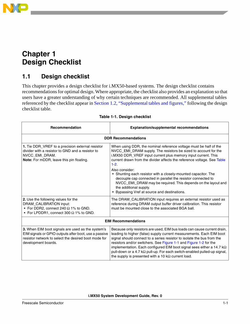
1.1 Design checklistThis chapter provides a design checklist for i.MX50-based systems. The design checklist contains recommendations for optimal design. Where appropriate, the checklist also provides an explanation so that users have a greater understanding of why certain techniques are recommended. All supplemental tables referenced by the checklist appear in Section 1.2, “Supplemental tables and figures,” following the design checklist table.
Table 1-1. Design checklist
Recommendation Explanation/supplemental recommendations
DDR Recommendations
1. Tie DDR_VREF to a precision external resistor divider with a resistor to GND and a resistor to NVCC_EMI_DRAM.Note: For mDDR, leave this pin floating.
When using DDR, the nominal reference voltage must be half of the NVCC_EMI_DRAM supply. The resistors be sized to account for the i.MX50 DDR_VREF input current plus memory input current. This current drawn from the divider affects the reference voltage. See Table 1-2.
Also consider: • Shunting each resistor with a closely-mounted capacitor. The
decouple cap connected in parallel the resistor connected to NVCC_EMI_DRAM may be required. This depends on the layout and the additional supply.
• Bypassing Vref at source and destinations.
2. Use the following values for the DRAM_CALIBRATION input: • For DDR2, connect 240 Ω 1% to GND. • For LPDDR1, connect 300 Ω 1% to GND.
The DRAM_CALIBRATION input requires an external resistor used as reference during DRAM output buffer driver calibration. This resistor must be mounted close to the associated BGA ball.
EIM Recommendations
3. When EIM boot signals are used as the system’s EIM signals or GPIO outputs after boot, use a passive resistor network to select the desired boot mode for development boards.
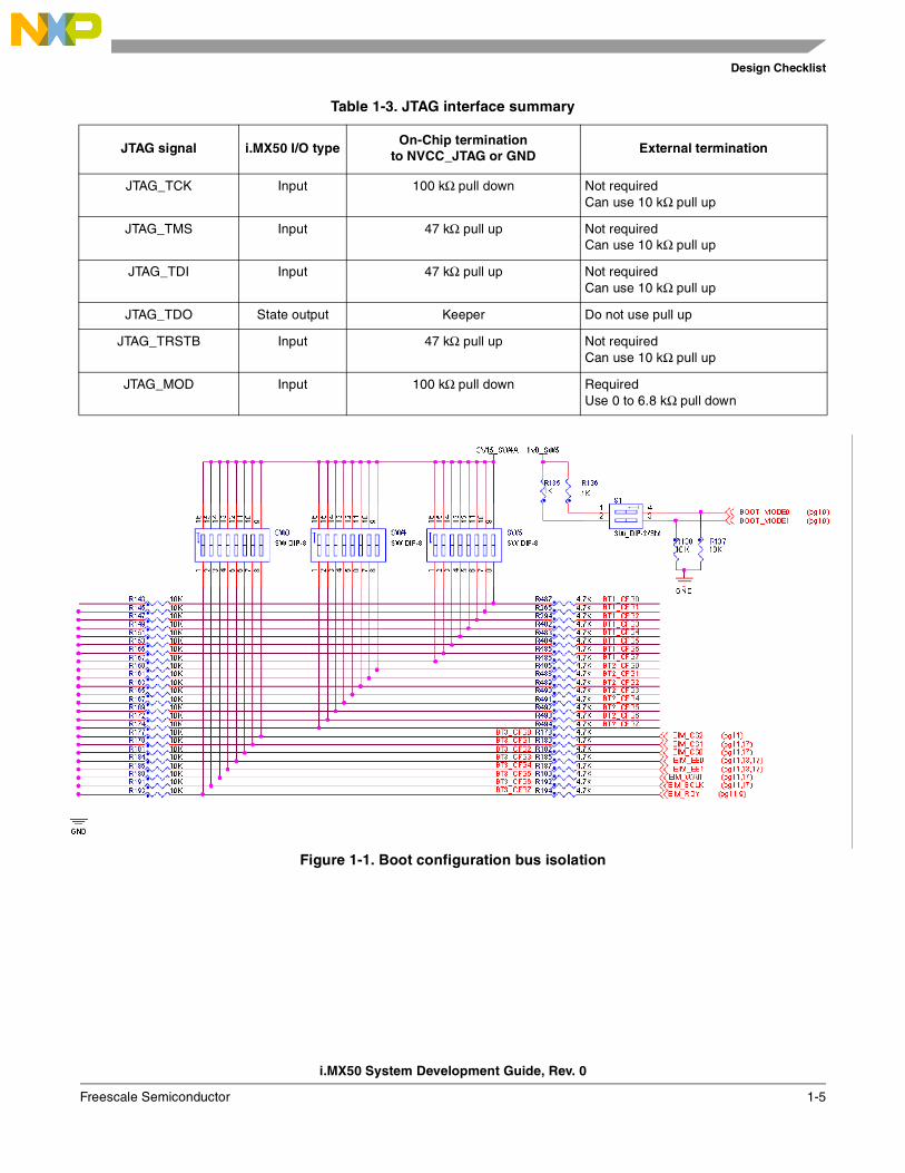
Because only resistors are used, EIM bus loads can cause current drain, leading to higher (false) supply current measurements. Each EIM boot signal should connect to a series resistor to isolate the bus from the resistors and/or switchers. See Figure 1-1 and Figure 1-2 for the implementation. Each configured EIM boot signal sees either a 14.7 kΩ pull-down or a 4.7 kΩ pull-up. For each switch-enabled pulled-up signal, the supply is presented with a 10 kΩ current load.
Design Checklist
i.MX50 System Development Guide, Rev. 0
1-2 Freescale Semiconductor
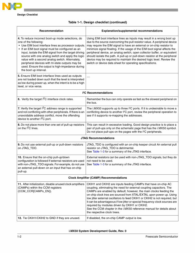
4. To reduce incorrect boot-up mode selections, do one of the following: • Use EIM boot interface lines as processor outputs. • If an EIM boot signal must be configured as an
input, isolate the EIM signal from the target driving source with one analog switch and apply the logic value with a second analog switch. Alternately, peripheral devices with tri-state outputs may be used. Ensure the output is high-impedance during the boot up interval.
Using EIM boot interface lines as inputs may result in a wrong boot up due to the source overcoming the pull resistor value. A peripheral device may require the EIM signal to have an external or on-chip resistor to minimize signal floating. If the usage of the EIM boot signal affects the peripheral device, an analog switch, open collector buffer, or equivalent should isolate the path. A pull-up or pull-down resistor at the peripheral device may be required to maintain the desired logic level. Review the switch or device data sheet for operating specifications.
5. Ensure EIM boot interface lines used as outputs are not loaded down such that the level is interpreted as low during power up, when the intent is to be a high level, or vice versa.
__
I2C Recommendations
6. Verify the target I2C interface clock rates. Remember the bus can only operate as fast as the slowest peripheral on the bus.
7. Verify the target I2C address range is supported and not conflicting with other peripherals. If there is an unavoidable address conflict, move the offending device to another I2C port.
The i.MX50 supports up to three I2C ports. If it is undesirable to move a conflicting device to another I2C port, review the peripheral operation to see if it supports re-mapping the addresses.
8. Do not place more than one set of pull-up resistors on the I2C lines.
This can result in excessive loading. Good design practice is to place a pair of pull-ups only on the schematic page that has the i.MX50 symbol. Do not place pull-ups on the pages with the I2C peripherals.
JTAG Recommendations
9. Do not use external pull-up or pull-down resistors on JTAG_TDO.
JTAG_TDO is configured with an on-chip keeper circuit An external pull resistor on JTAG_TDO is detrimental.See Table 1-3 for a summary of the JTAG interface.
10. Ensure that the on-chip pull-up/down configuration is followed If external resistors are used with non-JTAG_TDO signals. For example, do not use an external pull-down on an input that has on-chip pull-up.
External resistors can be used with non-JTAG_TDO signals, but they do not need to be used.See Table 1-3 for a summary of the JTAG interface.
Clock Amplifier (CAMP) Recommendations
11. After initialization, disable unused clock amplifiers (CAMPs) within the CCM registers (CCM_CCR[CAMPx_EN]).
CKIH1 and CKIH2 are inputs feeding CAMPs that have on-chip AC coupling, eliminating the need for external coupling capacitors. The CAMPs are enabled by default; however, the main clocks feeding the on-chip clock tree are sourced from XTAL/EXTAL upon power up. Using low jitter external oscillators to feed CKIH1 or CKIH2 is not required, but it can be advantageous if low jitter or special frequency clock sources are required by modules driven by CKIH1 or CKIH2.See the CCM chapter in the i.MX50 reference manual for details about the respective clock trees.
12. Tie CKIH1/CKIH2 to GND if they are unused. If disabled, the on-chip CAMP output is low.
Table 1-1. Design checklist (continued)
Recommendation Explanation/supplemental recommendations
Design Checklist
i.MX50 System Development Guide, Rev. 0
Freescale Semiconductor 1-3
Miscellaneous Signal Recommendations
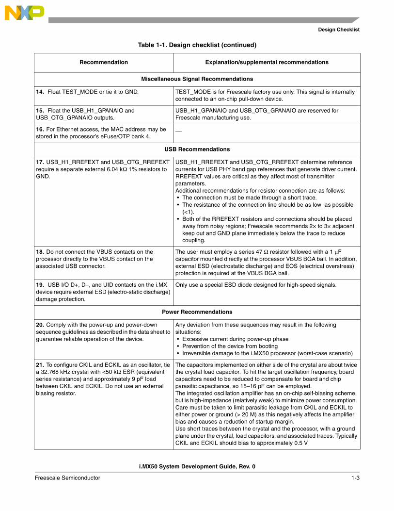
14. Float TEST_MODE or tie it to GND. TEST_MODE is for Freescale factory use only. This signal is internally connected to an on-chip pull-down device.
15. Float the USB_H1_GPANAIO and USB_OTG_GPANAIO outputs.
USB_H1_GPANAIO and USB_OTG_GPANAIO are reserved for Freescale manufacturing use.
16. For Ethernet access, the MAC address may be stored in the processor’s eFuse/OTP bank 4.
__
USB Recommendations
17. USB_H1_RREFEXT and USB_OTG_RREFEXT require a separate external 6.04 kΩ 1% resistors to GND.
USB_H1_RREFEXT and USB_OTG_RREFEXT determine reference currents for USB PHY band gap references that generate driver current. RREFEXT values are critical as they affect most of transmitter parameters. Additional recommendations for resistor connection are as follows: • The connection must be made through a short trace. • The resistance of the connection line should be as low as possible
(<1). • Both of the RREFEXT resistors and connections should be placed
away from noisy regions; Freescale recommends 2× to 3× adjacent keep out and GND plane immediately below the trace to reduce coupling.
18. Do not connect the VBUS contacts on the processor directly to the VBUS contact on the associated USB connector.
The user must employ a series 47 Ω resistor followed with a 1 μF capacitor mounted directly at the processor VBUS BGA ball. In addition, external ESD (electrostatic discharge) and EOS (electrical overstress) protection is required at the VBUS BGA ball.
19. USB I/O D+, D–, and UID contacts on the i.MX device require external ESD (electro-static discharge) damage protection.
Only use a special ESD diode designed for high-speed signals.
Power Recommendations
20. Comply with the power-up and power-down sequence guidelines as described in the data sheet to guarantee reliable operation of the device.
Any deviation from these sequences may result in the following situations: • Excessive current during power-up phase • Prevention of the device from booting • Irreversible damage to the i.MX50 processor (worst-case scenario)
21. To configure CKIL and ECKIL as an oscillator, tie a 32.768 kHz crystal with <50 kΩ ESR (equivalent series resistance) and approximately 9 pF load between CKIL and ECKIL. Do not use an external biasing resistor.
The capacitors implemented on either side of the crystal are about twice the crystal load capacitor. To hit the target oscillation frequency, board capacitors need to be reduced to compensate for board and chip parasitic capacitance, so 15–16 pF can be employed. The integrated oscillation amplifier has an on-chip self-biasing scheme, but is high-impedance (relatively weak) to minimize power consumption. Care must be taken to limit parasitic leakage from CKIL and ECKIL to either power or ground (> 20 M) as this negatively affects the amplifier bias and causes a reduction of startup margin.Use short traces between the crystal and the processor, with a ground plane under the crystal, load capacitors, and associated traces. Typically CKIL and ECKIL should bias to approximately 0.5 V
Table 1-1. Design checklist (continued)
Recommendation Explanation/supplemental recommendations
Design Checklist
i.MX50 System Development Guide, Rev. 0
1-4 Freescale Semiconductor
1.2 Supplemental tables and figures
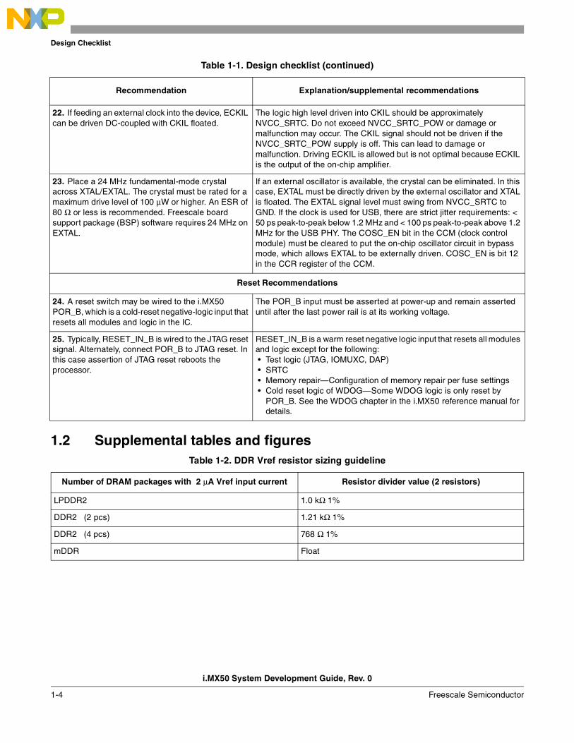
22. If feeding an external clock into the device, ECKIL can be driven DC-coupled with CKIL floated.
The logic high level driven into CKIL should be approximately NVCC_SRTC. Do not exceed NVCC_SRTC_POW or damage or malfunction may occur. The CKIL signal should not be driven if the NVCC_SRTC_POW supply is off. This can lead to damage or malfunction. Driving ECKIL is allowed but is not optimal because ECKIL is the output of the on-chip amplifier.
23. Place a 24 MHz fundamental-mode crystal across XTAL/EXTAL. The crystal must be rated for a maximum drive level of 100 μW or higher. An ESR of 80 Ω or less is recommended. Freescale board support package (BSP) software requires 24 MHz on EXTAL.
If an external oscillator is available, the crystal can be eliminated. In this case, EXTAL must be directly driven by the external oscillator and XTAL is floated. The EXTAL signal level must swing from NVCC_SRTC to GND. If the clock is used for USB, there are strict jitter requirements: < 50 ps peak-to-peak below 1.2 MHz and < 100 ps peak-to-peak above 1.2 MHz for the USB PHY. The COSC_EN bit in the CCM (clock control module) must be cleared to put the on-chip oscillator circuit in bypass mode, which allows EXTAL to be externally driven. COSC_EN is bit 12 in the CCR register of the CCM.
Reset Recommendations
24. A reset switch may be wired to the i.MX50 POR_B, which is a cold-reset negative-logic input that resets all modules and logic in the IC.
The POR_B input must be asserted at power-up and remain asserted until after the last power rail is at its working voltage.
25. Typically, RESET_IN_B is wired to the JTAG reset signal. Alternately, connect POR_B to JTAG reset. In this case assertion of JTAG reset reboots the processor.
RESET_IN_B is a warm reset negative logic input that resets all modules and logic except for the following: • Test logic (JTAG, IOMUXC, DAP) • SRTC • Memory repair—Configuration of memory repair per fuse settings • Cold reset logic of WDOG—Some WDOG logic is only reset by
POR_B. See the WDOG chapter in the i.MX50 reference manual for details.
Table 1-2. DDR Vref resistor sizing guideline
Number of DRAM packages with 2 μA Vref input current Resistor divider value (2 resistors)
LPDDR2 1.0 kΩ 1%
DDR2 (2 pcs) 1.21 kΩ 1%
DDR2 (4 pcs) 768 Ω 1%
mDDR Float
Table 1-1. Design checklist (continued)
Recommendation Explanation/supplemental recommendations
Design Checklist
i.MX50 System Development Guide, Rev. 0
Freescale Semiconductor 1-5
Figure 1-1. Boot configuration bus isolation
Table 1-3. JTAG interface summary
JTAG signal i.MX50 I/O typeOn-Chip termination
to NVCC_JTAG or GND External termination
JTAG_TCK Input 100 kΩ pull down Not requiredCan use 10 kΩ pull up
JTAG_TMS Input 47 kΩ pull up Not requiredCan use 10 kΩ pull up
JTAG_TDI Input 47 kΩ pull up Not requiredCan use 10 kΩ pull up
JTAG_TDO State output Keeper Do not use pull up
JTAG_TRSTB Input 47 kΩ pull up Not requiredCan use 10 kΩ pull up
JTAG_MOD Input 100 kΩ pull down RequiredUse 0 to 6.8 kΩ pull down
Design Checklist
i.MX50 System Development Guide, Rev. 0
1-6 Freescale Semiconductor
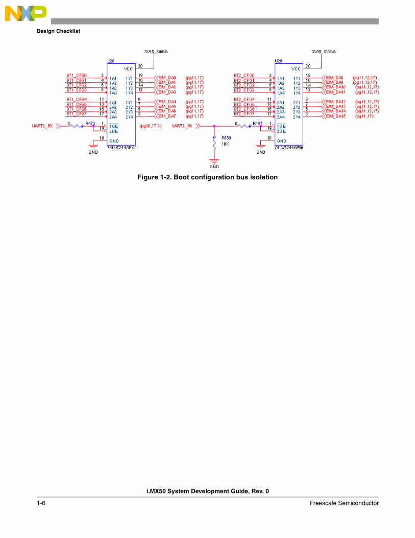
Figure 1-2. Boot configuration bus isolation

Configuring JTAG Tools for Debugging
i.MX50 System Development Guide, Rev. 0
Freescale Semiconductor 2-1
Chapter 2 Configuring JTAG Tools for DebuggingThis chapter explains how to configure JTAG tools for debugging. The JTAG module is a standard JEDEC debug peripheral. It provides debug access to important hardware blocks, such as the ARM processor and the system bus, which can give users access and control over the entire SoC. Because of this, unsecured JTAG modules are vulnerable to JTAG manipulation, a known hacker’s method of executing unauthorized program code, gaining control over secure applications, and running code in privileged modes. To properly secure the system, unauthorized JTAG usage must be strictly forbidden.
To prevent JTAG manipulation while allowing access for manufacturing tests and software debugging, the i.MX50 processor incorporates a secure JTAG controller for regulating JTAG access. The secure JTAG controller provides four different JTAG security modes, which are selected by an e-fuse configuration. For more information about the security modes, see the “Security” section in the “System JTAG Controller (SJC)” chapter of the i.MX50 reference manual.
NOTEBy default all parts are shipped with security disabled.
The JTAG port must be accessible during platform initial validation bring-up and for software debugging. It is accessible in all development kits from Freescale. Multiple tools are available for accessing the JTAG port for tests and software debugging. Freescale recommends use of the ARM JTAG tools for compatibility with the ARM core. However, the JTAG chain described in the following sections should work for non-ARM JTAG tools. For more information about non-ARM tools, contact the third party tool vendors for support.
2.1 Accessing debug with a JTAG scan chain (ARM tools)This section shows how to use the ARM tools to connect to the i.MX50 processor, using a JTAG scan chain. The example uses the RealView ICE (RVI) and RVDS ARM tools. RVI provides the hardware interface between the host PC and the JTAG port on the development kit (see http://www.arm.com/products/tools/rvi-and-rvt2.php for more information). RVDS is the software development kit that runs on the host PC. Its primary components consist of the ARM compiler, an Eclipse based IDE, and the RealView Debugger (for more information, see http://www.arm.com/products/tools/software-development-tools.php).
NOTE
Users must have the latest recommended ARM firmware installed on their RVI box to be able to connect to the Cortex-A8 on the i.MX50.
Once the latest firmware is installed, follow these steps to configure the JTAG scan chain on the RVI box:
1. Connect RVI to the i.MX50 board using the JTAG ribbon cable.
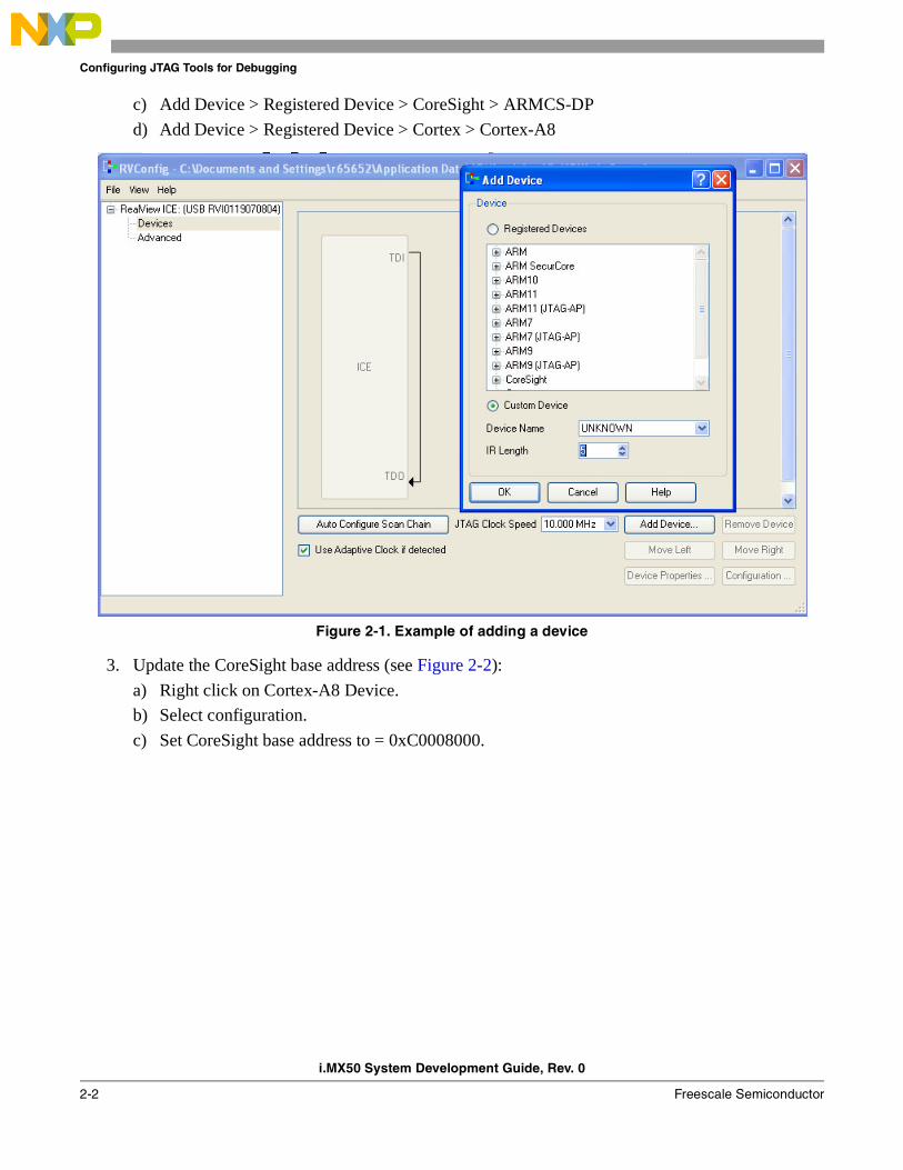
2. Using the order shown below, configure the scan chain with the following connections: TDI → Unknown → Unknown → ARMCS-DP → Cortex-A8 (see Figure 2-1).
a) Add Device > Custom Device > UNKNOWN > IR Length = 5
b) Add Device > Custom Device > UNKNOWN > IR Length = 4
Configuring JTAG Tools for Debugging
i.MX50 System Development Guide, Rev. 0
2-2 Freescale Semiconductor
c) Add Device > Registered Device > CoreSight > ARMCS-DP
d) Add Device > Registered Device > Cortex > Cortex-A8
Figure 2-1. Example of adding a device
3. Update the CoreSight base address (see Figure 2-2):
a) Right click on Cortex-A8 Device.
b) Select configuration.
c) Set CoreSight base address to = 0xC0008000.

Configuring JTAG Tools for Debugging
i.MX50 System Development Guide, Rev. 0
Freescale Semiconductor 2-3
Figure 2-2. Updating the CoreSight base address
4. Save the configuration.
Configuring JTAG Tools for Debugging
i.MX50 System Development Guide, Rev. 0
2-4 Freescale Semiconductor
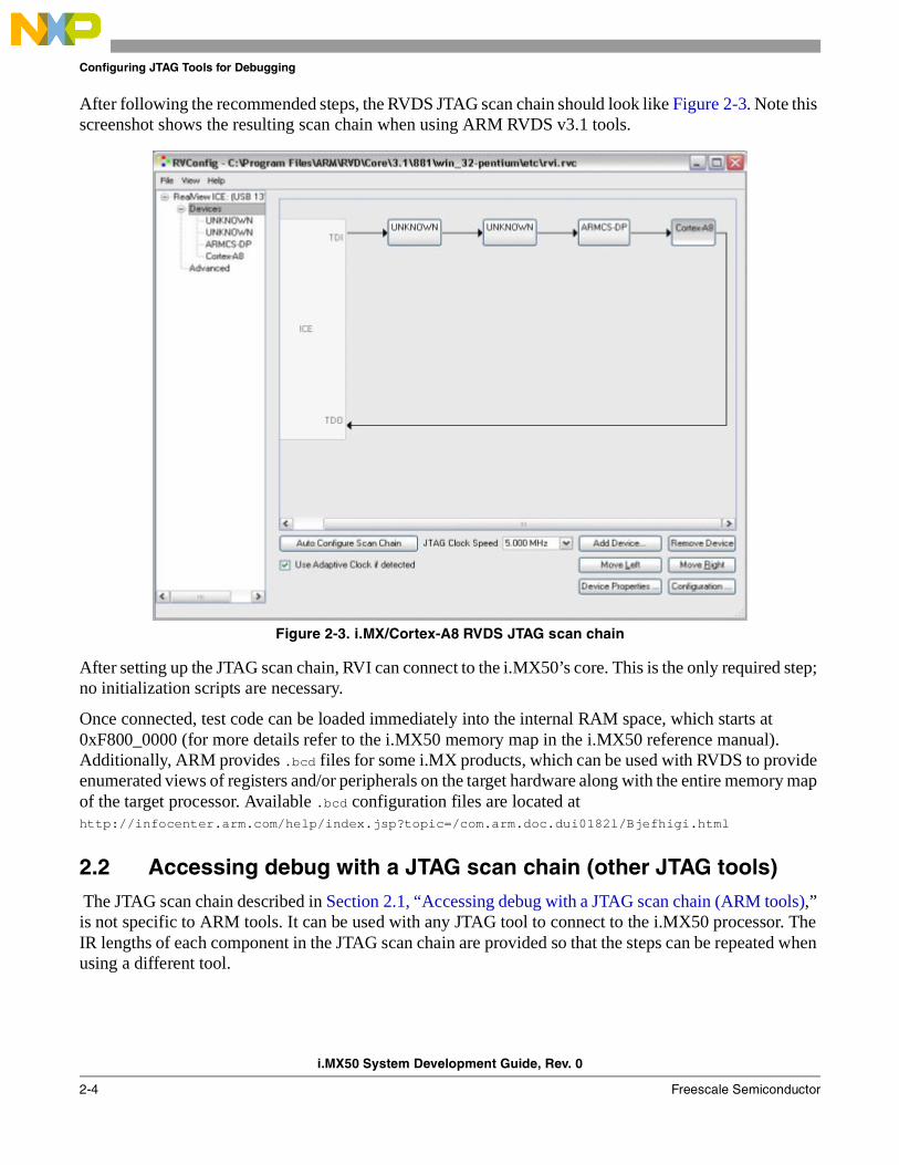
After following the recommended steps, the RVDS JTAG scan chain should look like Figure 2-3. Note this screenshot shows the resulting scan chain when using ARM RVDS v3.1 tools.
Figure 2-3. i.MX/Cortex-A8 RVDS JTAG scan chain
After setting up the JTAG scan chain, RVI can connect to the i.MX50’s core. This is the only required step; no initialization scripts are necessary.
Once connected, test code can be loaded immediately into the internal RAM space, which starts at 0xF800_0000 (for more details refer to the i.MX50 memory map in the i.MX50 reference manual). Additionally, ARM provides .bcd files for some i.MX products, which can be used with RVDS to provide enumerated views of registers and/or peripherals on the target hardware along with the entire memory map of the target processor. Available .bcd configuration files are located at http://infocenter.arm.com/help/index.jsp?topic=/com.arm.doc.dui0182l/Bjefhigi.html
2.2 Accessing debug with a JTAG scan chain (other JTAG tools) The JTAG scan chain described in Section 2.1, “Accessing debug with a JTAG scan chain (ARM tools),” is not specific to ARM tools. It can be used with any JTAG tool to connect to the i.MX50 processor. The IR lengths of each component in the JTAG scan chain are provided so that the steps can be repeated when using a different tool.

Avoiding Board Bring-Up Problems
i.MX50 System Development Guide, Rev. 0
Freescale Semiconductor 3-1
Chapter 3 Avoiding Board Bring-Up ProblemsThis chapter provides recommendations for avoiding typical mistakes when bringing up a board for the first time. These recommendations consist of basic techniques that have proven useful in the past for detecting board issues and address the three most typical bring-up pitfalls: power, clocks, and reset. A sample bring-up checklist is provided at the end of the chapter.
3.1 Using a voltage report to avoid power pitfallsUsing incorrect voltage rails is a common power pitfall. To help avoid this mistake, create a basic table called a voltage report prior to bringing up your board. This table helps validate that your supplies are coming to the expected level.
To create a voltage report, list the following:
• Your board voltage sources
• Default power-up values for the board voltage sources
• Best place on the board to measure the voltage level of each supply
Be careful when determining the best place to measure each supply. Depending on the location you take your measurement, a large voltage drop (IR drop) on the board may cause you to measure inaccurate levels.
The following guidelines help prevent this:
• Measure closest to the load (in this case the i.MX50 processor).
• Make two measurements: the first after initial board power-up and the second while running a heavy use-case that stresses the i.MX50.
The supplies that power the i.MX50 should all meet the DC electrical specifications as listed in the i.MX50 data sheet.
Table 3-1 shows a sample voltage report table.
Table 3-1. Sample voltage report table
Signal name Expected value (V)
Actual value (V) Test point Comments
5V_main 5.0 5.06 Pin1 of J5
LI-ON_Battery 4.2 4.18 Pin3 of J5
DCDC_3V15 3.15 3.14 R326
NVCC_SRTC 1.2 1.19 R73
VCC 1.2 1.19 R94
VDDA 1.2 1.19 R96
VDDAL 1.2 1.19 R96

Avoiding Board Bring-Up Problems
i.MX50 System Development Guide, Rev. 0
3-2 Freescale Semiconductor
3.2 Using a current monitor to avoid power pitfallsExcessive current can cause damage to the board. Avoid this problem by using a current-limiting laboratory supply that has a current read-out to power the main power to the board when bringing up the board for the first time. This allows the main power to be monitored, which makes it easy to detect any excessive current.
3.3 Checking for clock pitfallsProblems with the external clocks are another common source of board bring-up issues. Ensure that all of your clock sources are running as expected. The EXTAL/XTAL and the ECKIL/CKIL clocks are the main clock sources for 24 MHz and 32 kHz reference clocks respectively on the i.MX50. Although not required, the use of low jitter external oscillators to feed CKIH1 or CKIH2 on the i.MX50 can be an advantage if low jitter or special frequency clock sources are required by modules driven by CKIH1 or CKIH2. See the CCM chapter in the i.MX50 reference manual for details.
When checking crystal frequencies, use an active probe to avoid excessive loading. A parasitic probe typically inhibits the 32.768 kHz oscillator from starting up. Use the following guidelines:
• CKIL clock should be running at 32.768 kHz (can be generated internally or applied externally)
• EXTAL/EXTAL should be running at 24 MHz (used for the PLL reference)
VDDGP 1.05 1.09 R91
VDDO25 2.5 2.49 R370
NVCC_EMI_DRAM 1.8 1.79 R97
VREF 0.9 0.9 R201
NVCC (3.3 V IO) 3.15 3.14 R368
VDD3P0 3.15 3.14 R412
USB_OTG_VDDA33 3.15 3.14 R98
USB_H1_VDDA33 3.15 3.14 R98
NVCC (1.8 V IO) 1.8 1.79 R460
NVCC_RESET (LVIO) 1.8 1.79 R460
VDD2P5 2.5 2.49 R92
USB_OTG_VDDA25 2.5 2.49 R100
USB_H1_VDDA25 2.5 2.49 R100
VDD1P8 1.8 1.79 R93
VDD1P2 1.2 1.19 R95
Table 3-1. Sample voltage report table (continued)
Signal nameExpected value (V)
Actual value (V) Test point Comments
Avoiding Board Bring-Up Problems
i.MX50 System Development Guide, Rev. 0
Freescale Semiconductor 3-3
• CKIH1/CKIH2 can be used as oscillator inputs for low jitter special frequency sources.
• CKIH1 and CKIH2 are optional.
In addition to probing the external input clocks, you can check internal clocks by outputting them at the debug signals CLKO1 and CLKO2. See the CCM chapter in the i.MX50 reference manual for more details about which clock sources can be output to those debug signals.
3.4 Avoiding reset pitfallsFollow these guidelines to ensure that you use the correct boot mode to boot.
• During initial power on while asserting the POR_B reset signal, ensure that both your reference clocks are active before releasing POR_B.
• Follow the recommended power-up sequence specified in the i.MX50 reference manual.
The GPIOs and internal fuses control the i.MX50 boots. For a more detailed description about the different boot modes, refer to the system boot chapter of the i.MX50 reference manual.
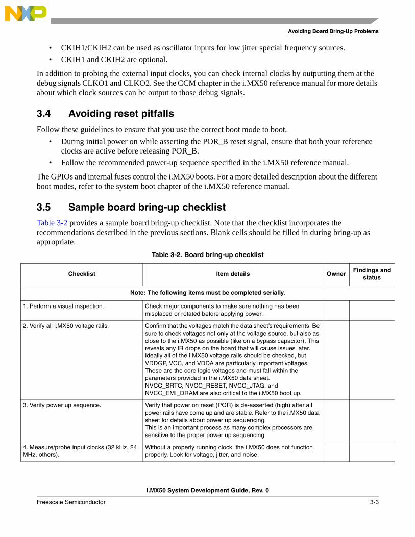
3.5 Sample board bring-up checklistTable 3-2 provides a sample board bring-up checklist. Note that the checklist incorporates the recommendations described in the previous sections. Blank cells should be filled in during bring-up as appropriate.
Table 3-2. Board bring-up checklist
Checklist Item details OwnerFindings and
status
Note: The following items must be completed serially.
1. Perform a visual inspection. Check major components to make sure nothing has been misplaced or rotated before applying power.
2. Verify all i.MX50 voltage rails. Confirm that the voltages match the data sheet’s requirements. Be sure to check voltages not only at the voltage source, but also as close to the i.MX50 as possible (like on a bypass capacitor). This reveals any IR drops on the board that will cause issues later.Ideally all of the i.MX50 voltage rails should be checked, but VDDGP, VCC, and VDDA are particularly important voltages. These are the core logic voltages and must fall within the parameters provided in the i.MX50 data sheet.NVCC_SRTC, NVCC_RESET, NVCC_JTAG, and NVCC_EMI_DRAM are also critical to the i.MX50 boot up.
3. Verify power up sequence. Verify that power on reset (POR) is de-asserted (high) after all power rails have come up and are stable. Refer to the i.MX50 data sheet for details about power up sequencing.This is an important process as many complex processors are sensitive to the proper power up sequencing.
4. Measure/probe input clocks (32 kHz, 24 MHz, others).
Without a properly running clock, the i.MX50 does not function properly. Look for voltage, jitter, and noise.
Avoiding Board Bring-Up Problems
i.MX50 System Development Guide, Rev. 0
3-4 Freescale Semiconductor
5. Check JTAG connectivity (RV-ICE). This is one of the most fundamental and basic access points to the i.MX50 to allow the debug and execution of low level code.
Note: The following items may be worked on in parallel with other bring up tasks.
6. Access internal RAM. Verify basic operation of the i.MX50 in system. The on-chip internal RAM starts at address 0xF800_0000 and is 128 Kbytes in density. Perform a basic test by performing a write-read-verify to the internal RAM. No software initialization is necessary to access internal RAM.
7. Verify CLKO outputs (measure and verify default clock frequencies for desired clock output options) if the board design supports probing of the CLKO pin.
This ensures that the corresponding clock is working and that the PLLs are working.Note that this step requires chip initialization—for example via the JTAG debugger—to properly set up the IOMUX to output CLKO and to set up the clock control module to output the desired clock. Refer to the reference manual for more details.
8. Measure boot mode frequencies. Set the boot mode switch for each boot mode and measure the following (depending on system availability): • NAND (probe CE to verify boot,
measure RE frequency) • SPI-NOR (probe slave select and
measure clock frequency) • MMC/SD (measure clock frequency)
This verifies the specified signals’ connectivity between the i.MX50 and boot device and that the boot mode signals are properly set. Refer to the “Boot Modes for the i.MX50” section in the i.MX50 reference manual for details about configuring the various boot modes.
9. Run basic DDR initialization and test memory.
1. Assuming the use of a JTAG debugger, run the DDR initialization and open a debugger memory window pointing to the DDR memory map starting address.
2. Try writing a few words and verify that they can be read correctly.
3. If not, recheck the DDR initialization sequence and whether the DDR has been correctly soldered onto the board.
It is also recommended that users recheck the schematic and PCB layout to ensure that the DDR memory has been connected to the i.MX50 correctly.
Table 3-2. Board bring-up checklist (continued)
Checklist Item details OwnerFindings and
status

Using the Clock Connectivity Table
i.MX50 System Development Guide, Rev. 0
Freescale Semiconductor 4-1
Chapter 4 Using the Clock Connectivity TableThis chapter explains how to use the i.MX50 clocking connectivity. You can use this information to save power by disabling clocks to unused modules.
4.1 External clock sourcesThe following list describes the external clock sources:
• RTC 32.768KHz CKIL/ECKIL crystal—This is a 32.768 kHz crystal input for the i.MX50. By default, ECKIL comes from Ripley PMIC output.
• 24 MHz XTAL/EXTAL crystal—This is a 24 MHz input for the i.MX50. The required accuracy of this crystal is 50 ppm.
• 12.288 MHz oscillator—This oscillator is for the audio codec. The required accuracy of this crystal is 30 ppm.
• 50 MHz oscillator—This oscillator is for Ethernet. The required accuracy of this crystal is 30 ppm.
4.2 Internal clock sourcesFor information about how the root clocks are generated, see the clock generation diagrams in the CCM chapter of the i.MX50 reference manual. In some cases, the CCM does not generate the clock, and the clock may come directly from the IO pad.
The following list shows a reference setting for the CCM registers.
• mx50 pll1: 800 MHz
• mx50 pll2: 400 MHz
• mx50 pll3: 216 MHz
• ipg clock : 66666666 Hz
• ipg per clock : 66666666 Hz
• uart clock : 24000000 Hz
• ahb clock : 133333333 Hz
• axi_a clock : 400000000 Hz
• axi_b clock : 200000000 Hz
• weim_clock : 100000000 Hz
• ddr clock : 266666666 Hz
• esdhc1 clock : 80000000 Hz
• esdhc2 clock : 80000000 Hz
• esdhc3 clock : 80000000 Hz
• esdhc4 clock : 80000000 Hz
• GPMI clock : 24000000 Hz
• BCH clock : 24000000 Hz
Using the Clock Connectivity Table
i.MX50 System Development Guide, Rev. 0
4-2 Freescale Semiconductor
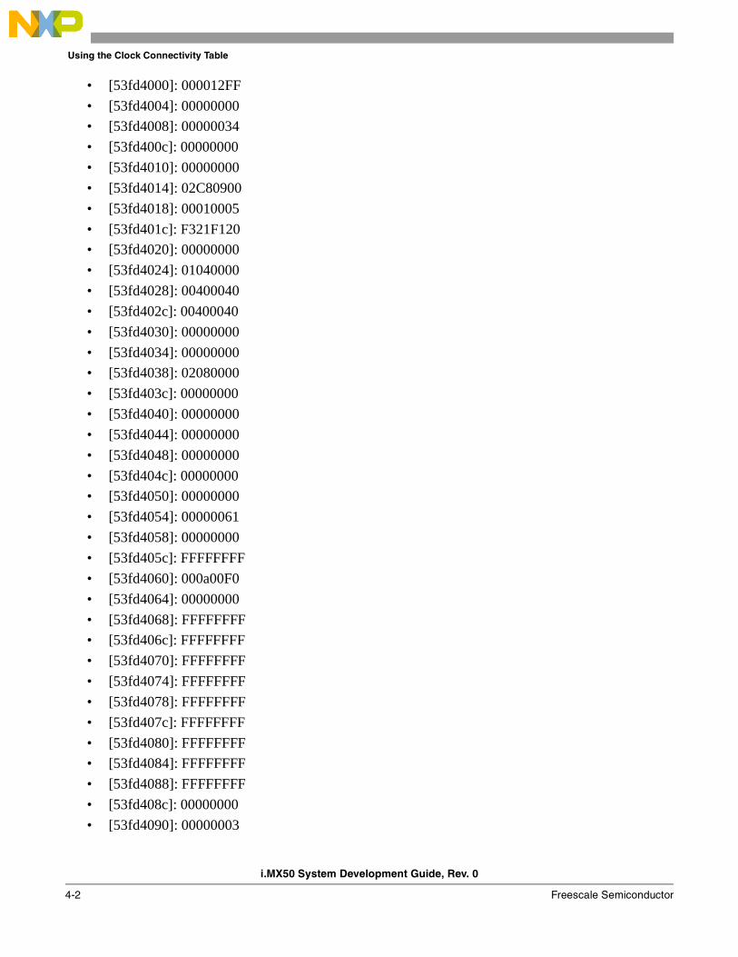
• [53fd4000]: 000012FF
• [53fd4004]: 00000000
• [53fd4008]: 00000034
• [53fd400c]: 00000000
• [53fd4010]: 00000000
• [53fd4014]: 02C80900
• [53fd4018]: 00010005
• [53fd401c]: F321F120
• [53fd4020]: 00000000
• [53fd4024]: 01040000
• [53fd4028]: 00400040
• [53fd402c]: 00400040
• [53fd4030]: 00000000
• [53fd4034]: 00000000
• [53fd4038]: 02080000
• [53fd403c]: 00000000
• [53fd4040]: 00000000
• [53fd4044]: 00000000
• [53fd4048]: 00000000
• [53fd404c]: 00000000
• [53fd4050]: 00000000
• [53fd4054]: 00000061
• [53fd4058]: 00000000
• [53fd405c]: FFFFFFFF
• [53fd4060]: 000a00F0
• [53fd4064]: 00000000
• [53fd4068]: FFFFFFFF
• [53fd406c]: FFFFFFFF
• [53fd4070]: FFFFFFFF
• [53fd4074]: FFFFFFFF
• [53fd4078]: FFFFFFFF
• [53fd407c]: FFFFFFFF
• [53fd4080]: FFFFFFFF
• [53fd4084]: FFFFFFFF
• [53fd4088]: FFFFFFFF
• [53fd408c]: 00000000
• [53fd4090]: 00000003

Using the Clock Connectivity Table
i.MX50 System Development Guide, Rev. 0
Freescale Semiconductor 4-3
• [53fd4094]: A0000044
• [53fd4098]: 80000003
• [53fd409c]: 00001001
• [53fd40a0]: 00001001
• [53fd40a4]: 00000001
• [53fd40a8]: 00000001
• [53fd40ac]: 80000001
• [53fd40b0]: 80000001
• [53fd40b4]: 00000001
Clock connectivity is described in the “System Clocks Connectivity” section in the CCM chapter of the i.MX50 reference manual. This section contains a series of tables that describe the clock inputs of each module and which clock is connected to it. In most cases, the clocks are CCM root clocks. However, some clocks come from IO pins (mainly though IOMUX) and not from CCM.
Clock gating is done with the low power clock gating (LPCG) module based on a combination of the clock enable signals. For more information about how the clock gating signals are logically combined, refer to the LPCG section in the CCM chapter of the i.MX50 reference manual.
NOTEIn some cases, a clock is part of a protocol and is sourced from a pad (mainly through IOMUX). Such clocks do not appear in the clock connectivity table. They are found in the “External Signals and Pin Multiplexing” chapter.

Using the Clock Connectivity Table
i.MX50 System Development Guide, Rev. 0
4-4 Freescale Semiconductor

i.MX50 System Development Guide, Rev. 0
Freescale Semiconductor 5-1
Chapter 5 About the IOMUX Tool
5.1 IOMUX: What is it?The i.MX applications processor has a limited number of IO connections relative to all possible signals available to the on-chip peripherals. The input-output multiplexer (IOMUX) is the on-chip multiplexer that connects the package pins or balls to the internal peripheral signals.
Each IO connection has the following three registers:
• MUX control register—controls which internal signal is connected to a particular external IO connection
• Pad control register—controls the electrical behavior of the IO cell connected to the external IO connection
• Input select register—controls the connection between an internal input signal and the external IO connection.
Every signal that is routed through the IOMUX requires that the first two registers be properly set. In addition, if the input select register is not properly configured, the external input will not be connected to the internal peripheral (an omission often made by those unfamiliar with configuring the IOMUX).
For more specific information about the IOMUX module, refer to the appropriate i.MX applications processor’s reference manual.
5.2 How the IOMUX tool helps application designIt is difficult to make all the assignments for an application without introducing conflicts between signals and IO connections. If not caught before a board was produced, such conflicts may even require board revisions to correct. The IOMUX tool was developed to help the hardware system designer make these signal assignments and to resolve conflicts more easily. A secondary purpose of the tool is to provide system documentation for the hardware and software developers.
5.2.1 Assigning signals and resolving conflicts
The main purpose of the IOMUX tool is to allow real time assignment with immediate conflict detection. A Windows GUI interface consisting of nested check boxes allows users to assign individual signals or whole peripherals. For each signal, users can choose a specific external IO connection (ball or pin). If the assignment results in a definite conflict, the tool highlights the conflicting signals in orange. If the assignment results in a potential conflict, the tool highlights the potentially conflicting signal in yellow. Users can then avoid the conflict either by avoiding that particular signal assignment or if that particular external IO connection is desired, reassigning the existing assignment(s).
About the IOMUX Tool
i.MX50 System Development Guide, Rev. 0
5-2 Freescale Semiconductor
Contextual information boxes are available when the mouse hovers over the different portions of the GUI. These boxes provide information that helps users avoid and/or resolve assignment conflicts. A pictorial diagram of the device package is also provided so that the relative location of the signals and their external IO connection assignments can be inspected.
5.2.2 Documentation features
The IOMUX tool allows a design to be saved to and loaded from a file to allow multi-session design development. It also allows the creation of derivative boards based on an existing design.
A novel feature of the IOMUX tool is the ability to annotate signal assignments with “Signal Notes.” One such use is to associate application specific signal names with each signal assignment so the intended use can be related to the i.MX device’s IO connections and internal signals. General information about the application, revision level, contact information, and other design related information may be entered as well.
In addition to the ability to load and save a design in the native XML format, application design information can be printed or saved as either plain text or rich text format (RTF). The plain text information can then be pasted into the schematic files, readily providing the assignment information during hardware debug. The plain text information may also be pasted into the application software source repository, providing software developers with the assignment information all in one place.
The output includes the GPIO signals that are available at every external IO connection. This information can be useful during board bring-up because it readily allows individual IO connections to be wiggled to diagnose connectivity issues at the board level without needing to run a stack to support the functional operation of a peripheral.
5.2.3 Additional features
Mismatches between the signal levels at the board level and the IO connections of the i.MX applications processor can occur when peripheral signals are assigned to external IO connections that are not supplied by the same power supply rails. To help users ensure that signal levels match between the device and the rest of the board, the IOMUX tool allows the assignment of voltages to each power supply. For each peripheral used in the design, the user will be alerted where a mismatch in power supply voltages for a peripheral exists.
5.3 Obtaining the IOMUX toolThe IOMUX tool may be downloaded from the Freescale web page at the IOMUX Tool download location. More complete documentation about the tool and its features are included in the download (about 1 MB in size).

Setting up Power Management
i.MX50 System Development Guide, Rev. 0
Freescale Semiconductor 6-1
Chapter 6 Setting up Power ManagementThis chapter discusses how to supply and interface the i.MX50 multimedia applications processor with power management integrated circuits (PMICs): MC34708 from Freescale.
The interface requires the addition of an extra RT8011A regulator to supply the external DCDC 3.15 V power domain. Note that the DCDC is needed only when a large current external device exists, such as WIFI or 3G. Otherwise, we can use the supply from the PMIC.
6.1 i.MX50 power requirement
6.1.1 Voltage rail and current requirement for i.MX50
Table 6-1. Voltage rail and current requirements
Power Rail of i.MX50 Power domain Max current (mA) Voltage (V)
NVCC_SRTC 32 kHz osc. power (when chip off) TBD1 1.20
VCC LP Transistor power 400 1.20
VDDA Peripheral Memory + L2 Cache power 250 1.20
VDDAL1 L1 Cache power 250 1.20
VDDGP Core and G Transistor power 1250 1.00
VDDO2P5 Predriver for EMI pads 150 2.50
NVCC_EMI_DRAM Power to EMI pins 350 1.20
VREF DRAM Reference 2~4 μA 0.9
All 3.3 V IO NVCC 3.0 V I/Os — —
VDD3P0 VDD2P5 LDO input + power to Bandgap, DCDC predriver, tempsensor, 480 MHz PLL
~10 3.00
USB_OTG_VDDA33 Power to USB Host 16 3.30
USB_H1_VDDA33 Power to USB OTG 16 3.30
All 1.8V IO NVCC 1.8 V I/Os — —
NVCC_RESET (LVIO) Power to POR_B,RESET_IN_B, TESTMODE, & BOOTMODE[0:1]
Few(TBD)1 TBD1
VDD2P5 Power to 24 MHz osc, efuse, xtalok, 32 kHz osc. power mux
~10 2.50
USB_OTG_VDDA25 Power to USB Host 50 2.50
USB_H1_VDDA25 Power to USB OTG 50 2.50
VDD1P8 Power to all PLLs ~10 1.80

Setting up Power Management
i.MX50 System Development Guide, Rev. 0
6-2 Freescale Semiconductor
6.1.2 Power-up sequence requirement for i.MX50
Figure 6-1. i.MX50 power-up sequence
VDD1P2 Power to all PLL digital, 32 kHz osc. (when chip on), much of analog, digital
~10 1.20
1. TBD means to refer to the actual design load.
Table 6-1. Voltage rail and current requirements (continued)
Power Rail of i.MX50 Power domain Max current (mA) Voltage (V)
NVCC_SRTC
VCC
VDDGPVDDAVDDAL1 VDD3P0 VDDO2P5
VDD2P5
VDD1P8 VDD1P2
NVCC_EMI_DRAM
VREF
USB_OTG_VDDA25USB_H1_VDDA25
USB_OTG_VDDA33
USB_H1_VDDA33
Note:No power-up sequence dependencies exist between the supplies shown shaded in gray.
NVCC_EIMNVCC_EPDCNVCC_JTAGNVCC_KEYPADNVCC_LCDNVCC_MISCNVCC_NANDF
NVCC_RESETNVCC_SD1NVCC_SD2NVCC_SSINVCC_UART
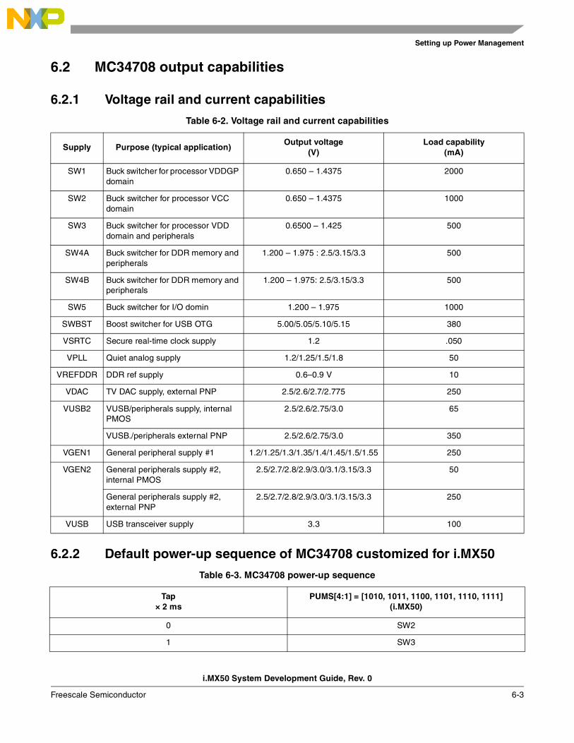
Setting up Power Management
i.MX50 System Development Guide, Rev. 0
Freescale Semiconductor 6-3
6.2 MC34708 output capabilities
6.2.1 Voltage rail and current capabilities
6.2.2 Default power-up sequence of MC34708 customized for i.MX50
Table 6-2. Voltage rail and current capabilities
Supply Purpose (typical application)Output voltage
(V)Load capability
(mA)
SW1 Buck switcher for processor VDDGP domain
0.650 – 1.4375 2000
SW2 Buck switcher for processor VCC domain
0.650 – 1.4375 1000
SW3 Buck switcher for processor VDD domain and peripherals
0.6500 – 1.425 500
SW4A Buck switcher for DDR memory and peripherals
1.200 – 1.975 : 2.5/3.15/3.3 500
SW4B Buck switcher for DDR memory and peripherals
1.200 – 1.975: 2.5/3.15/3.3 500
SW5 Buck switcher for I/O domin 1.200 – 1.975 1000
SWBST Boost switcher for USB OTG 5.00/5.05/5.10/5.15 380
VSRTC Secure real-time clock supply 1.2 .050
VPLL Quiet analog supply 1.2/1.25/1.5/1.8 50
VREFDDR DDR ref supply 0.6–0.9 V 10
VDAC TV DAC supply, external PNP 2.5/2.6/2.7/2.775 250
VUSB2 VUSB/peripherals supply, internal PMOS
2.5/2.6/2.75/3.0 65
VUSB./peripherals external PNP 2.5/2.6/2.75/3.0 350
VGEN1 General peripheral supply #1 1.2/1.25/1.3/1.35/1.4/1.45/1.5/1.55 250
VGEN2 General peripherals supply #2, internal PMOS
2.5/2.7/2.8/2.9/3.0/3.1/3.15/3.3 50
General peripherals supply #2, external PNP
2.5/2.7/2.8/2.9/3.0/3.1/3.15/3.3 250
VUSB USB transceiver supply 3.3 100
Table 6-3. MC34708 power-up sequence
Tap× 2 ms
PUMS[4:1] = [1010, 1011, 1100, 1101, 1110, 1111](i.MX50)
0 SW2
1 SW3

Setting up Power Management
i.MX50 System Development Guide, Rev. 0
6-4 Freescale Semiconductor
6.2.3 Power-up voltage rail
MC34708 is a PMIC designed to support the i.MX family. MC34708 sets the specific power-up sequence by 5 GPIO. The voltage level of PUMS[5:1] decides the power-up sequence mode.
Figure 6-4. Power-up mode
2 SW1A/B
3 VDAC
4 SW4A/B, VREFDDR
5 SW5
6 VGEN2
7 VPLL
8 VGEN1
9 VUSB (2), VUSB2
1 The VUSB regulator is only enabled if 5 V is present on the VBUS pin. By default, VUSB is supplied by the VBUS pin.
Table 6-3. MC34708 power-up sequence (continued)
Tap× 2 ms
PUMS[4:1] = [1010, 1011, 1100, 1101, 1110, 1111](i.MX50)
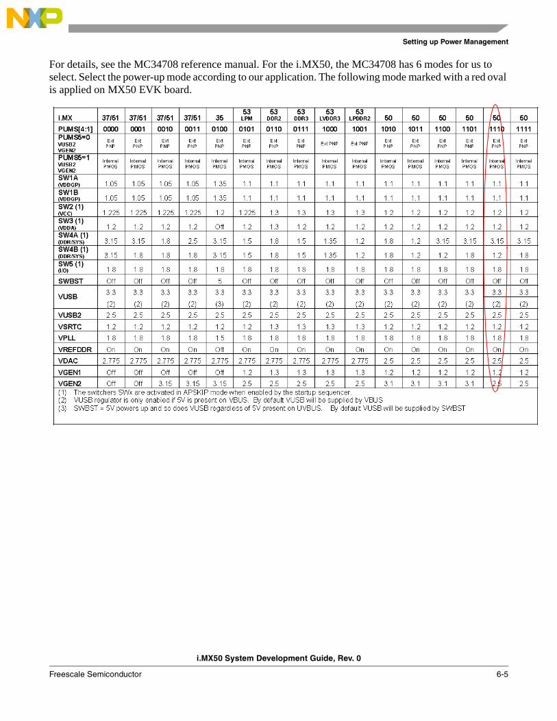
Setting up Power Management
i.MX50 System Development Guide, Rev. 0
Freescale Semiconductor 6-5
For details, see the MC34708 reference manual. For the i.MX50, the MC34708 has 6 modes for us to select. Select the power-up mode according to our application. The following mode marked with a red oval is applied on MX50 EVK board.
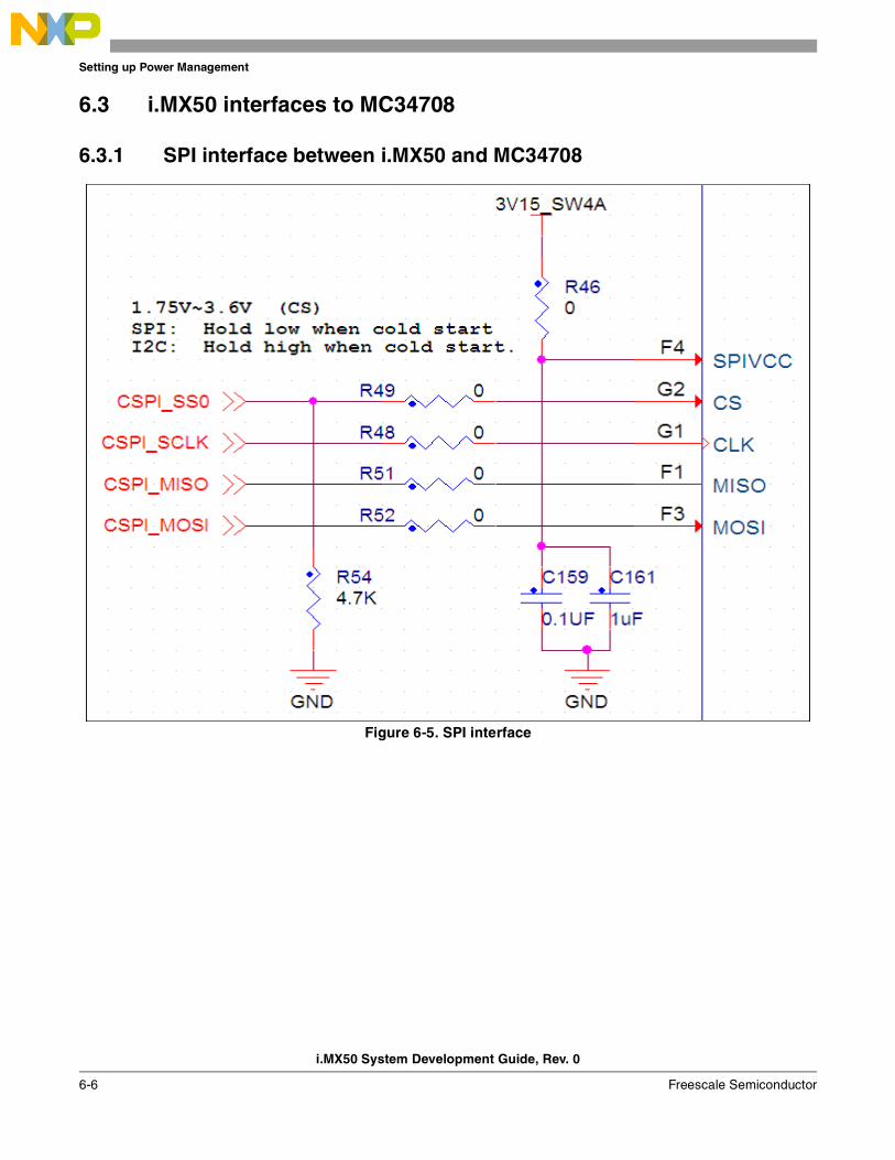
Setting up Power Management
i.MX50 System Development Guide, Rev. 0
6-6 Freescale Semiconductor
6.3 i.MX50 interfaces to MC34708
6.3.1 SPI interface between i.MX50 and MC34708
Figure 6-5. SPI interface
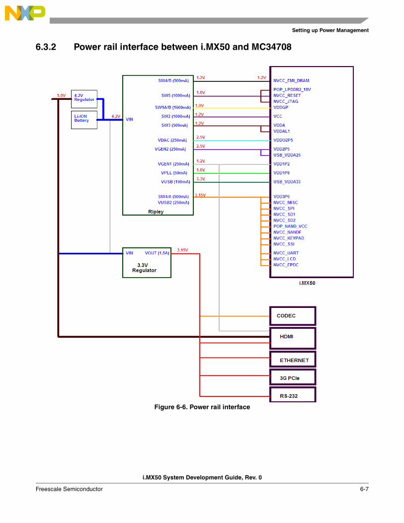
Setting up Power Management
i.MX50 System Development Guide, Rev. 0
Freescale Semiconductor 6-7
6.3.2 Power rail interface between i.MX50 and MC34708
Figure 6-6. Power rail interface
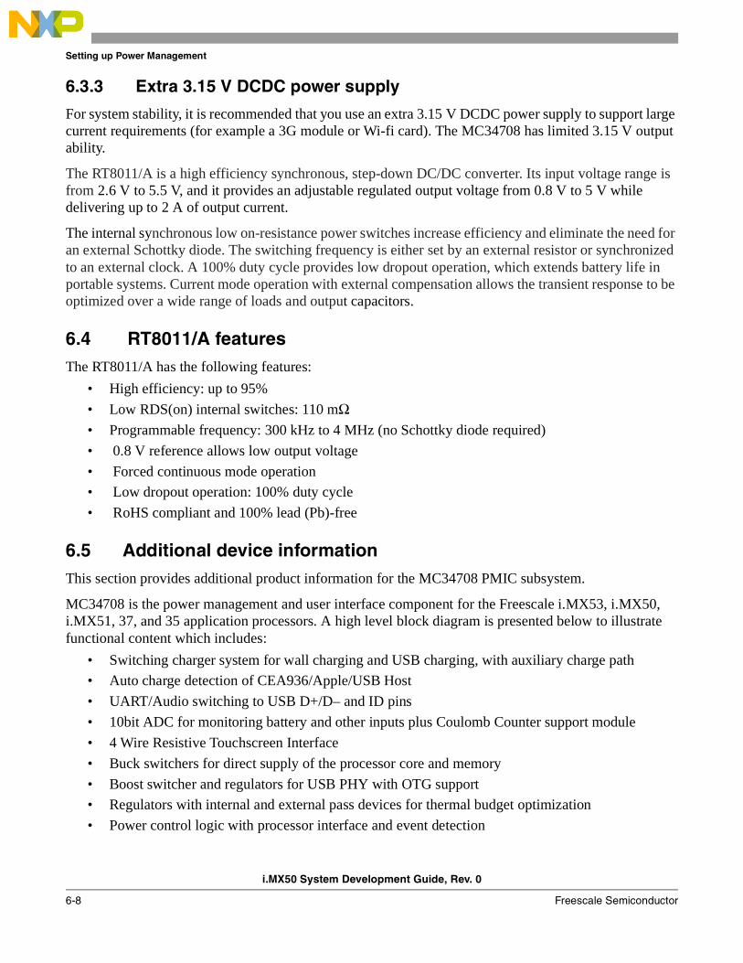
Setting up Power Management
i.MX50 System Development Guide, Rev. 0
6-8 Freescale Semiconductor
6.3.3 Extra 3.15 V DCDC power supply
For system stability, it is recommended that you use an extra 3.15 V DCDC power supply to support large current requirements (for example a 3G module or Wi-fi card). The MC34708 has limited 3.15 V output ability.
The RT8011/A is a high efficiency synchronous, step-down DC/DC converter. Its input voltage range is from 2.6 V to 5.5 V, and it provides an adjustable regulated output voltage from 0.8 V to 5 V while delivering up to 2 A of output current.
The internal synchronous low on-resistance power switches increase efficiency and eliminate the need for an external Schottky diode. The switching frequency is either set by an external resistor or synchronized to an external clock. A 100% duty cycle provides low dropout operation, which extends battery life in portable systems. Current mode operation with external compensation allows the transient response to be optimized over a wide range of loads and output capacitors.
6.4 RT8011/A featuresThe RT8011/A has the following features:
• High efficiency: up to 95%
• Low RDS(on) internal switches: 110 mΩ• Programmable frequency: 300 kHz to 4 MHz (no Schottky diode required)
• 0.8 V reference allows low output voltage
• Forced continuous mode operation
• Low dropout operation: 100% duty cycle
• RoHS compliant and 100% lead (Pb)-free
6.5 Additional device informationThis section provides additional product information for the MC34708 PMIC subsystem.
MC34708 is the power management and user interface component for the Freescale i.MX53, i.MX50, i.MX51, 37, and 35 application processors. A high level block diagram is presented below to illustrate functional content which includes:
• Switching charger system for wall charging and USB charging, with auxiliary charge path
• Auto charge detection of CEA936/Apple/USB Host
• UART/Audio switching to USB D+/D– and ID pins
• 10bit ADC for monitoring battery and other inputs plus Coulomb Counter support module
• 4 Wire Resistive Touchscreen Interface
• Buck switchers for direct supply of the processor core and memory
• Boost switcher and regulators for USB PHY with OTG support
• Regulators with internal and external pass devices for thermal budget optimization
• Power control logic with processor interface and event detection
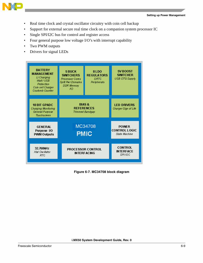
Setting up Power Management
i.MX50 System Development Guide, Rev. 0
Freescale Semiconductor 6-9
• Real time clock and crystal oscillator circuitry with coin cell backup
• Support for external secure real time clock on a companion system processor IC
• Single SPI/I2C bus for control and register access
• Four general purpose low voltage I/O’s with interrupt capability
• Two PWM outputs
• Drivers for signal LEDs
Figure 6-7. MC34708 block diagram
MC34708

Interfacing DDR Memories with the i.MX50 Processor
i.MX50 System Development Guide, Rev. 0
Freescale Semiconductor 7-1
Chapter 7 Interfacing DDR Memories with the i.MX50 Processor
7.1 OverviewThe i.MX50 supports off-chip DRAM storage using the DRAM MC, which is connected to the internal AXI bus. The DRAM MC supports multiple external memory types, including:
• Standard 1.8 V DDR2
• 1.8 V Mobile DDR1 (LP-DDR1)
• 1.2 V Mobile DDR2 (LP-DDR2)
The DRAM MC consists of three major components:
• AXI bus interface
• DRAM controller
• DRAM PHY
The DRAM MC uses three primary clocks: the AHB bus clock (HCLK), the AXI bus clock (AXI_CLK), and the DDR interface clock (DDR_CLK). The AXI_CLK and DDR_CLK can be configured as either synchronous or asynchronous, but the HCLK and AXI_CLK are always treated asynchronously.
The DRAM MC supports the following clock frequencies:
• Up to 266 MHz at the DDR interface (532 MHz data rate)
• Up to 266 MHz at the AXI interface
• Up to 133 MHz at the AHB interface

Interfacing DDR Memories with the i.MX50 Processor
i.MX50 System Development Guide, Rev. 0
7-2 Freescale Semiconductor
7.2 Connection between i.MX50 and DDR memoriesFigure 7-1–Figure 7-3 show various interfaces between i.MX50 and DDR memories.
Figure 7-1. Interfacing between i.MX50 and LPDDR2
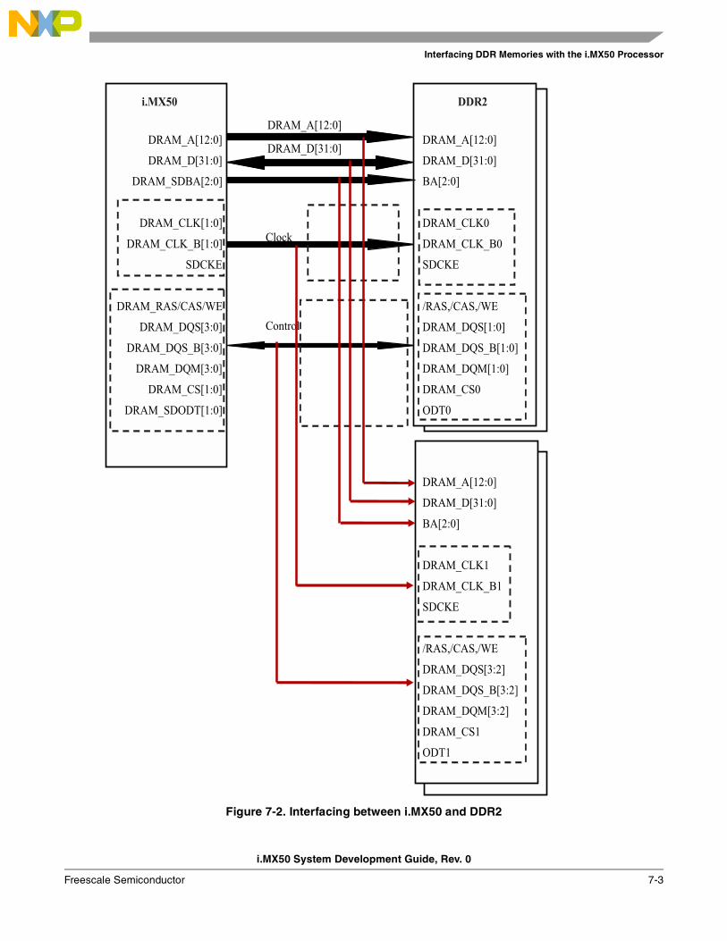
Interfacing DDR Memories with the i.MX50 Processor
i.MX50 System Development Guide, Rev. 0
Freescale Semiconductor 7-3
Figure 7-2. Interfacing between i.MX50 and DDR2
Interfacing DDR Memories with the i.MX50 Processor
i.MX50 System Development Guide, Rev. 0
7-4 Freescale Semiconductor
Figure 7-3. Interfacing between i.MX50 and mDDR
When using DDR, the nominal reference voltage must be half of the NVCC_EMI_DRAM supply. The resistors must be sized to account for the i.MX50 DDR_VREF input current plus the memory input current. This current, drawn from the divider, affects the reference voltage.
Consider:• Shunting each resistor with a closely-mounted capacitor. The decouple cap connected in parallel
to the resistor connected to NVCC_EMI_DRAM may be required.
• Tie DDR_VREF to a precision external resistor divider with a resistor to GND and a resistor to NVCC_EMI_DRAM.
For the resistors selection, please refer to Table 1-2.
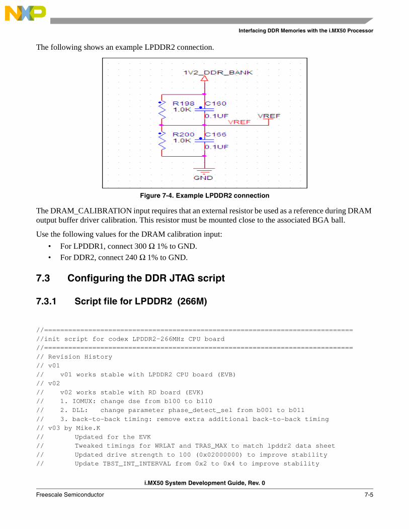
Interfacing DDR Memories with the i.MX50 Processor
i.MX50 System Development Guide, Rev. 0
Freescale Semiconductor 7-5
The following shows an example LPDDR2 connection.
Figure 7-4. Example LPDDR2 connection
The DRAM_CALIBRATION input requires that an external resistor be used as a reference during DRAM output buffer driver calibration. This resistor must be mounted close to the associated BGA ball.
Use the following values for the DRAM calibration input:
• For LPDDR1, connect 300 Ω 1% to GND.
• For DDR2, connect 240 Ω 1% to GND.
7.3 Configuring the DDR JTAG script
7.3.1 Script file for LPDDR2 (266M)
//=============================================================================//init script for codex LPDDR2-266MHz CPU board//=============================================================================// Revision History// v01// v01 works stable with LPDDR2 CPU board (EVB)// v02// v02 works stable with RD board (EVK)// 1. IOMUX: change dse from b100 to b110// 2. DLL: change parameter phase_detect_sel from b001 to b011// 3. back-to-back timing: remove extra additional back-to-back timing// v03 by Mike.K// Updated for the EVK// Tweaked timings for WRLAT and TRAS_MAX to match lpddr2 data sheet// Updated drive strength to 100 (0x02000000) to improve stability// Update TBST_INT_INTERVAL from 0x2 to 0x4 to improve stability
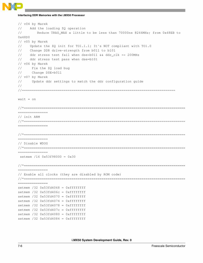
Interfacing DDR Memories with the i.MX50 Processor
i.MX50 System Development Guide, Rev. 0
7-6 Freescale Semiconductor
// v04 by Marek// Add the loading ZQ operation// Reduce TRAS_MAX a little to be less than 70000ns @266MHz; from 0x48EB to 0x48D0// v05 by Marek// Update the ZQ init for TO1.1.1; It's NOT compliant with TO1.0// Change DDR drive-strength from b011 to b101// ddr stress test fail when dse=b011 && ddr_clk >= 200MHz// ddr stress test pass when dse=b101// v06 by Marek// Fix the ZQ load bug// Change DSE=b011// v07 by Marek// Update ddr settings to match the ddr configuration guide// //=============================================================================
wait = on
//*================================================================================================// init ARM//*================================================================================================ //*================================================================================================// Disable WDOG//*================================================================================================ setmem /16 0x53f98000 = 0x30
//*================================================================================================// Enable all clocks (they are disabled by ROM code)//*================================================================================================setmem /32 0x53fd4068 = 0xffffffffsetmem /32 0x53fd406c = 0xffffffffsetmem /32 0x53fd4070 = 0xffffffffsetmem /32 0x53fd4074 = 0xffffffffsetmem /32 0x53fd4078 = 0xffffffffsetmem /32 0x53fd407c = 0xffffffffsetmem /32 0x53fd4080 = 0xffffffffsetmem /32 0x53fd4084 = 0xffffffff
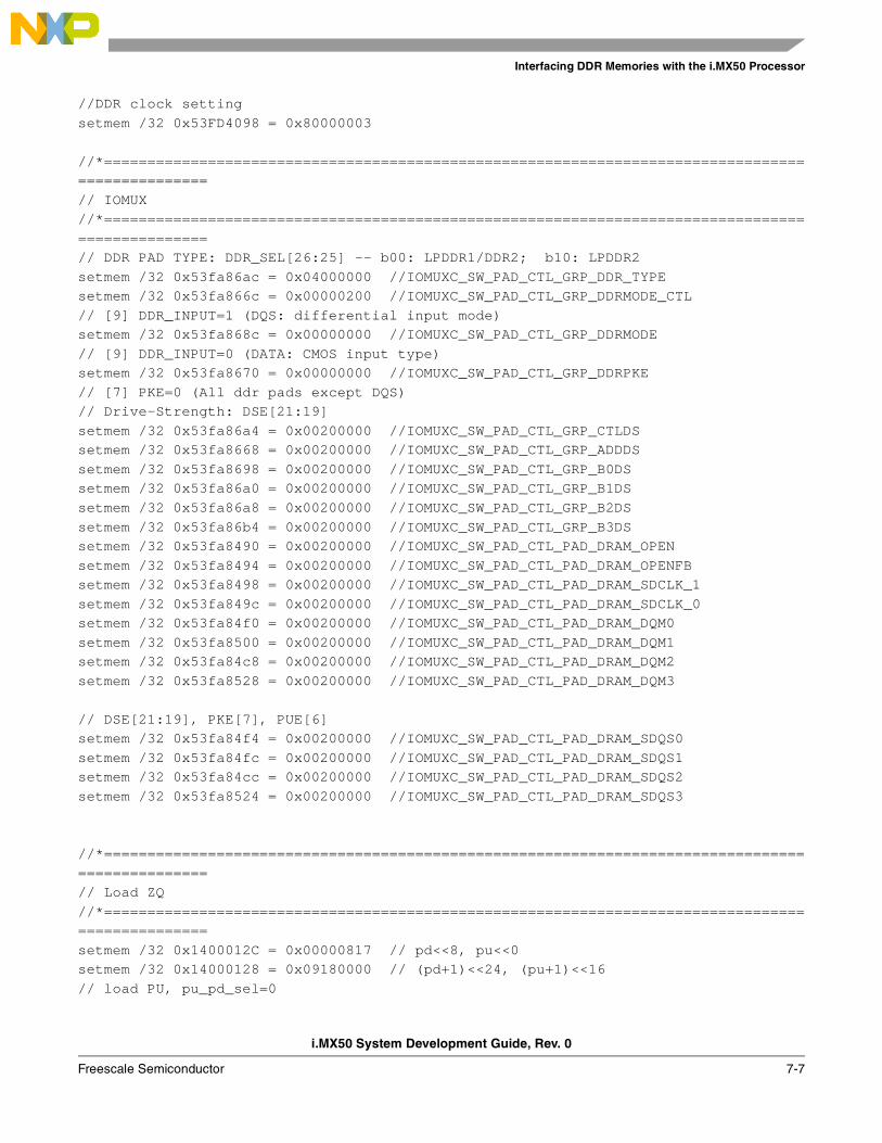
Interfacing DDR Memories with the i.MX50 Processor
i.MX50 System Development Guide, Rev. 0
Freescale Semiconductor 7-7
//DDR clock settingsetmem /32 0x53FD4098 = 0x80000003 //*================================================================================================// IOMUX//*================================================================================================// DDR PAD TYPE: DDR_SEL[26:25] -- b00: LPDDR1/DDR2; b10: LPDDR2setmem /32 0x53fa86ac = 0x04000000 //IOMUXC_SW_PAD_CTL_GRP_DDR_TYPEsetmem /32 0x53fa866c = 0x00000200 //IOMUXC_SW_PAD_CTL_GRP_DDRMODE_CTL// [9] DDR_INPUT=1 (DQS: differential input mode)setmem /32 0x53fa868c = 0x00000000 //IOMUXC_SW_PAD_CTL_GRP_DDRMODE// [9] DDR_INPUT=0 (DATA: CMOS input type)setmem /32 0x53fa8670 = 0x00000000 //IOMUXC_SW_PAD_CTL_GRP_DDRPKE// [7] PKE=0 (All ddr pads except DQS)// Drive-Strength: DSE[21:19]setmem /32 0x53fa86a4 = 0x00200000 //IOMUXC_SW_PAD_CTL_GRP_CTLDSsetmem /32 0x53fa8668 = 0x00200000 //IOMUXC_SW_PAD_CTL_GRP_ADDDSsetmem /32 0x53fa8698 = 0x00200000 //IOMUXC_SW_PAD_CTL_GRP_B0DSsetmem /32 0x53fa86a0 = 0x00200000 //IOMUXC_SW_PAD_CTL_GRP_B1DSsetmem /32 0x53fa86a8 = 0x00200000 //IOMUXC_SW_PAD_CTL_GRP_B2DSsetmem /32 0x53fa86b4 = 0x00200000 //IOMUXC_SW_PAD_CTL_GRP_B3DSsetmem /32 0x53fa8490 = 0x00200000 //IOMUXC_SW_PAD_CTL_PAD_DRAM_OPENsetmem /32 0x53fa8494 = 0x00200000 //IOMUXC_SW_PAD_CTL_PAD_DRAM_OPENFBsetmem /32 0x53fa8498 = 0x00200000 //IOMUXC_SW_PAD_CTL_PAD_DRAM_SDCLK_1setmem /32 0x53fa849c = 0x00200000 //IOMUXC_SW_PAD_CTL_PAD_DRAM_SDCLK_0setmem /32 0x53fa84f0 = 0x00200000 //IOMUXC_SW_PAD_CTL_PAD_DRAM_DQM0setmem /32 0x53fa8500 = 0x00200000 //IOMUXC_SW_PAD_CTL_PAD_DRAM_DQM1setmem /32 0x53fa84c8 = 0x00200000 //IOMUXC_SW_PAD_CTL_PAD_DRAM_DQM2setmem /32 0x53fa8528 = 0x00200000 //IOMUXC_SW_PAD_CTL_PAD_DRAM_DQM3
// DSE[21:19], PKE[7], PUE[6]setmem /32 0x53fa84f4 = 0x00200000 //IOMUXC_SW_PAD_CTL_PAD_DRAM_SDQS0setmem /32 0x53fa84fc = 0x00200000 //IOMUXC_SW_PAD_CTL_PAD_DRAM_SDQS1setmem /32 0x53fa84cc = 0x00200000 //IOMUXC_SW_PAD_CTL_PAD_DRAM_SDQS2setmem /32 0x53fa8524 = 0x00200000 //IOMUXC_SW_PAD_CTL_PAD_DRAM_SDQS3
//*================================================================================================// Load ZQ//*================================================================================================setmem /32 0x1400012C = 0x00000817 // pd<<8, pu<<0setmem /32 0x14000128 = 0x09180000 // (pd+1)<<24, (pu+1)<<16// load PU, pu_pd_sel=0
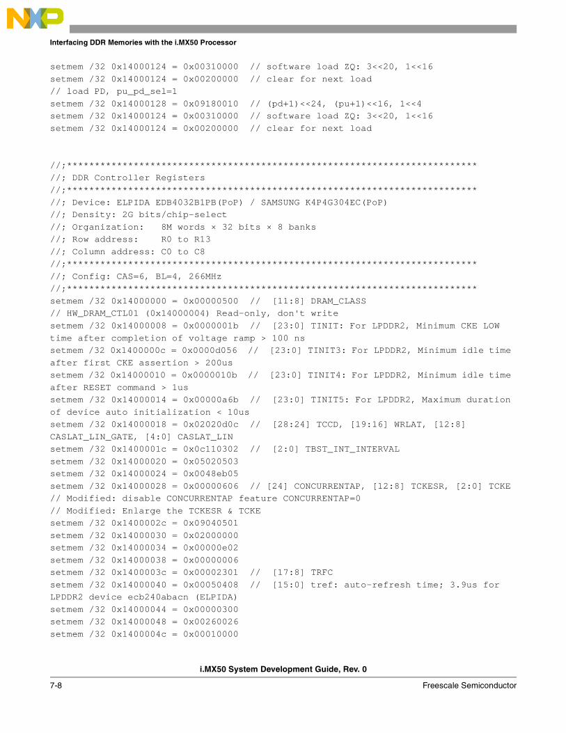
Interfacing DDR Memories with the i.MX50 Processor
i.MX50 System Development Guide, Rev. 0
7-8 Freescale Semiconductor
setmem /32 0x14000124 = 0x00310000 // software load ZQ: 3<<20, 1<<16setmem /32 0x14000124 = 0x00200000 // clear for next load// load PD, pu_pd_sel=1setmem /32 0x14000128 = 0x09180010 // (pd+1)<<24, (pu+1)<<16, 1<<4setmem /32 0x14000124 = 0x00310000 // software load ZQ: 3<<20, 1<<16setmem /32 0x14000124 = 0x00200000 // clear for next load
//;**************************************************************************//; DDR Controller Registers//;**************************************************************************//; Device: ELPIDA EDB4032B1PB(PoP) / SAMSUNG K4P4G304EC(PoP)//; Density: 2G bits/chip-select//; Organization: 8M words × 32 bits × 8 banks//; Row address: R0 to R13//; Column address: C0 to C8//;**************************************************************************//; Config: CAS=6, BL=4, 266MHz//;**************************************************************************setmem /32 0x14000000 = 0x00000500 // [11:8] DRAM_CLASS// HW_DRAM_CTL01 (0x14000004) Read-only, don't writesetmem /32 0x14000008 = 0x0000001b // [23:0] TINIT: For LPDDR2, Minimum CKE LOW time after completion of voltage ramp > 100 nssetmem /32 0x1400000c = 0x0000d056 // [23:0] TINIT3: For LPDDR2, Minimum idle time after first CKE assertion > 200ussetmem /32 0x14000010 = 0x0000010b // [23:0] TINIT4: For LPDDR2, Minimum idle time after RESET command > 1ussetmem /32 0x14000014 = 0x00000a6b // [23:0] TINIT5: For LPDDR2, Maximum duration of device auto initialization < 10ussetmem /32 0x14000018 = 0x02020d0c // [28:24] TCCD, [19:16] WRLAT, [12:8] CASLAT_LIN_GATE, [4:0] CASLAT_LINsetmem /32 0x1400001c = 0x0c110302 // [2:0] TBST_INT_INTERVALsetmem /32 0x14000020 = 0x05020503setmem /32 0x14000024 = 0x0048eb05setmem /32 0x14000028 = 0x00000606 // [24] CONCURRENTAP, [12:8] TCKESR, [2:0] TCKE// Modified: disable CONCURRENTAP feature CONCURRENTAP=0// Modified: Enlarge the TCKESR & TCKEsetmem /32 0x1400002c = 0x09040501setmem /32 0x14000030 = 0x02000000setmem /32 0x14000034 = 0x00000e02setmem /32 0x14000038 = 0x00000006setmem /32 0x1400003c = 0x00002301 // [17:8] TRFCsetmem /32 0x14000040 = 0x00050408 // [15:0] tref: auto-refresh time; 3.9us for LPDDR2 device ecb240abacn (ELPIDA)setmem /32 0x14000044 = 0x00000300setmem /32 0x14000048 = 0x00260026setmem /32 0x1400004c = 0x00010000

Interfacing DDR Memories with the i.MX50 Processor
i.MX50 System Development Guide, Rev. 0
Freescale Semiconductor 7-9
setmem /32 0x14000050 = 0x00000000 // lowpower modesetmem /32 0x14000054 = 0x00000000 // lowpower modesetmem /32 0x14000058 = 0x00000000 // lowpower modesetmem /32 0x1400005c = 0x02000000setmem /32 0x14000060 = 0x00000002 // [8] write-mode-reg; [3:0] CKSRXsetmem /32 0x14000064 = 0x00000000 // [16:0] read-mode-regsetmem /32 0x14000068 = 0x00000000 // [31:16] MR0_DATA_0; [15:0] MRR_DATAsetmem /32 0x1400006c = 0x00040042 // [31:16] MR2_DATA_0; [15:0] MR1_DATA_0setmem /32 0x14000070 = 0x00000001 // [31:16] MR16_DATA_0; [15:0] MR3_DATA_0setmem /32 0x14000074 = 0x00000000 // [31:16] MR0_DATA_1; [15:0] MR17_DATA_0setmem /32 0x14000078 = 0x00040042 // [31:16] MR2_DATA_1; [15:0] MR1_DATA_1setmem /32 0x1400007c = 0x00000001 // [31:16] MR16_DATA_1; [15:0] MR3_DATA_1setmem /32 0x14000080 = 0x010b0000 // [27:16] ZQINIT; [15:0] MR17_DATA_1setmem /32 0x14000084 = 0x00000060 // ZQsetmem /32 0x14000088 = 0x02400018 // ZQsetmem /32 0x1400008c = 0x01000e00 // ZQsetmem /32 0x14000090 = 0x0a010101 // [18:16] COLUMN_SIZE; [10:8] ADDR-PINS; [0] EIGHT_BANK_MODEsetmem /32 0x14000094 = 0x01011f1fsetmem /32 0x14000098 = 0x01010101setmem /32 0x1400009c = 0x00030101 // [24] REDUC: select 16/32-bit mode; [17:16] CS_MAPsetmem /32 0x140000a0 = 0x00010000 // [16] LPDDR2_S4=1setmem /32 0x140000a4 = 0x00010000 // [16] RESYNC_DLL_PER_AREF_EN; [8] RESYNC_DLLsetmem /32 0x140000a8 = 0x00000000 // [25:16] INT_ACK; [10:0] INT_STATUSsetmem /32 0x140000ac = 0x00000fff // [10:0] INT_MASK// HW_DRAM_CTL44~49 (0x140000b0~c4) Read-only, don't writesetmem /32 0x140000c8 = 0x02020101 // ODTsetmem /32 0x140000cc = 0x01000000 // ODTsetmem /32 0x140000d0 = 0x01000201 // Additonal Delaysetmem /32 0x140000d4 = 0x00000200 // Additonal Delaysetmem /32 0x140000d8 = 0x00000102setmem /32 0x140000dc = 0x0000ffff // [17:16] AXI0_FIFO_TYPE_REG// Modified: setmem /32 0x140000e0 = 0x0000ff00 // No meaning for this MCsetmem /32 0x140000e4 = 0x02020000 // AXI0setmem /32 0x140000e8 = 0x02020202 // AXI0setmem /32 0x140000ec = 0x00000202 // AXI0setmem /32 0x140000f0 = 0x01010064 // AXI1setmem /32 0x140000f4 = 0x01010101 // AXI1setmem /32 0x140000f8 = 0x00010101 // AXI0setmem /32 0x140000fc = 0x00000064 // [16] CKE_STATUSsetmem /32 0x14000100 = 0x00000000setmem /32 0x14000104 = 0x02000802 // DFIsetmem /32 0x14000108 = 0x04080000 // DFIsetmem /32 0x1400010c = 0x04080408 // DFIsetmem /32 0x14000110 = 0x04080408 // DFI
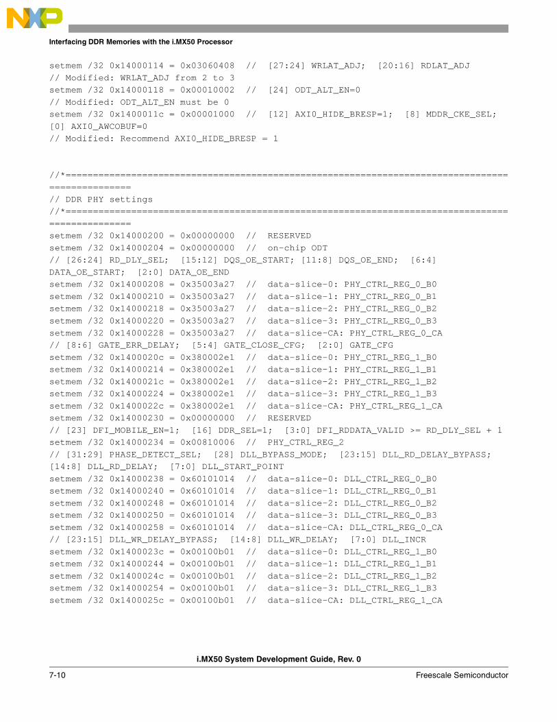
Interfacing DDR Memories with the i.MX50 Processor
i.MX50 System Development Guide, Rev. 0
7-10 Freescale Semiconductor
setmem /32 0x14000114 = 0x03060408 // [27:24] WRLAT_ADJ; [20:16] RDLAT_ADJ// Modified: WRLAT_ADJ from 2 to 3setmem /32 0x14000118 = 0x00010002 // [24] ODT_ALT_EN=0// Modified: ODT_ALT_EN must be 0setmem /32 0x1400011c = 0x00001000 // [12] AXI0_HIDE_BRESP=1; [8] MDDR_CKE_SEL; [0] AXI0_AWCOBUF=0// Modified: Recommend AXI0_HIDE_BRESP = 1
//*================================================================================================// DDR PHY settings//*================================================================================================setmem /32 0x14000200 = 0x00000000 // RESERVEDsetmem /32 0x14000204 = 0x00000000 // on-chip ODT// [26:24] RD_DLY_SEL; [15:12] DQS_OE_START; [11:8] DQS_OE_END; [6:4] DATA_OE_START; [2:0] DATA_OE_ENDsetmem /32 0x14000208 = 0x35003a27 // data-slice-0: PHY_CTRL_REG_0_B0setmem /32 0x14000210 = 0x35003a27 // data-slice-1: PHY_CTRL_REG_0_B1setmem /32 0x14000218 = 0x35003a27 // data-slice-2: PHY_CTRL_REG_0_B2setmem /32 0x14000220 = 0x35003a27 // data-slice-3: PHY_CTRL_REG_0_B3setmem /32 0x14000228 = 0x35003a27 // data-slice-CA: PHY_CTRL_REG_0_CA// [8:6] GATE_ERR_DELAY; [5:4] GATE_CLOSE_CFG; [2:0] GATE_CFGsetmem /32 0x1400020c = 0x380002e1 // data-slice-0: PHY_CTRL_REG_1_B0setmem /32 0x14000214 = 0x380002e1 // data-slice-1: PHY_CTRL_REG_1_B1setmem /32 0x1400021c = 0x380002e1 // data-slice-2: PHY_CTRL_REG_1_B2setmem /32 0x14000224 = 0x380002e1 // data-slice-3: PHY_CTRL_REG_1_B3setmem /32 0x1400022c = 0x380002e1 // data-slice-CA: PHY_CTRL_REG_1_CAsetmem /32 0x14000230 = 0x00000000 // RESERVED// [23] DFI_MOBILE_EN=1; [16] DDR_SEL=1; [3:0] DFI_RDDATA_VALID >= RD_DLY_SEL + 1setmem /32 0x14000234 = 0x00810006 // PHY_CTRL_REG_2// [31:29] PHASE_DETECT_SEL; [28] DLL_BYPASS_MODE; [23:15] DLL_RD_DELAY_BYPASS; [14:8] DLL_RD_DELAY; [7:0] DLL_START_POINTsetmem /32 0x14000238 = 0x60101014 // data-slice-0: DLL_CTRL_REG_0_B0setmem /32 0x14000240 = 0x60101014 // data-slice-1: DLL_CTRL_REG_0_B1setmem /32 0x14000248 = 0x60101014 // data-slice-2: DLL_CTRL_REG_0_B2setmem /32 0x14000250 = 0x60101014 // data-slice-3: DLL_CTRL_REG_0_B3setmem /32 0x14000258 = 0x60101014 // data-slice-CA: DLL_CTRL_REG_0_CA// [23:15] DLL_WR_DELAY_BYPASS; [14:8] DLL_WR_DELAY; [7:0] DLL_INCRsetmem /32 0x1400023c = 0x00100b01 // data-slice-0: DLL_CTRL_REG_1_B0setmem /32 0x14000244 = 0x00100b01 // data-slice-1: DLL_CTRL_REG_1_B1setmem /32 0x1400024c = 0x00100b01 // data-slice-2: DLL_CTRL_REG_1_B2setmem /32 0x14000254 = 0x00100b01 // data-slice-3: DLL_CTRL_REG_1_B3setmem /32 0x1400025c = 0x00100b01 // data-slice-CA: DLL_CTRL_REG_1_CA
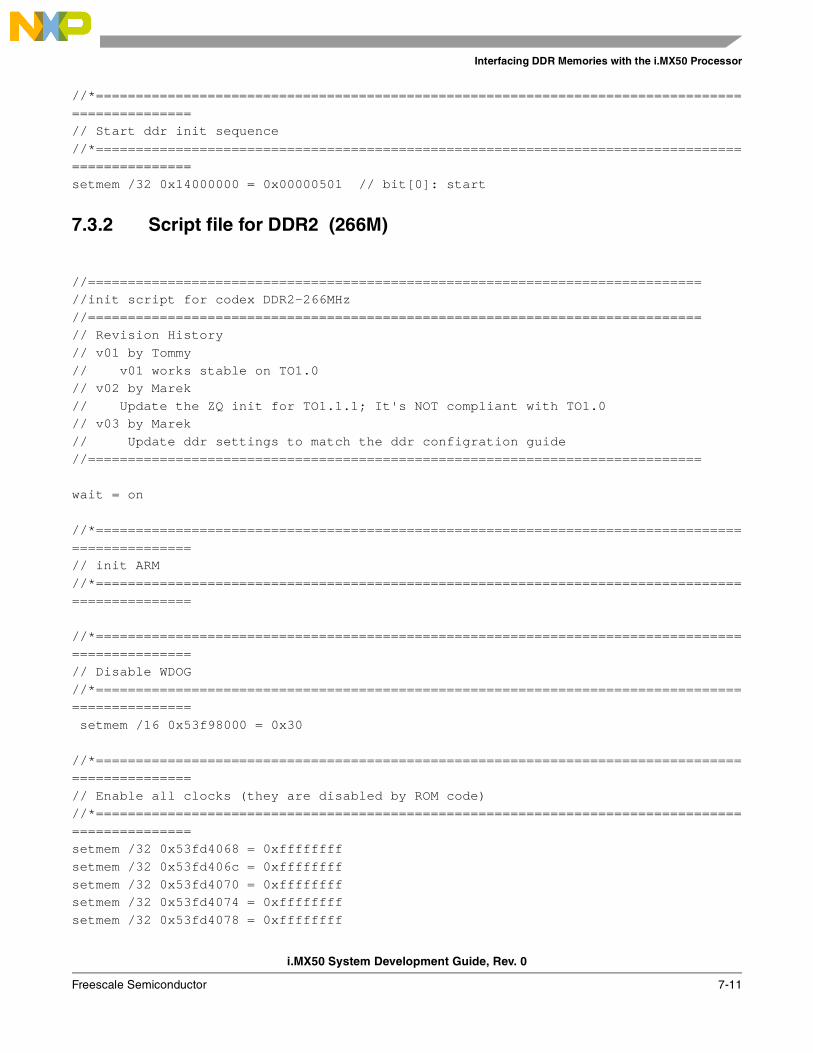
Interfacing DDR Memories with the i.MX50 Processor
i.MX50 System Development Guide, Rev. 0
Freescale Semiconductor 7-11
//*================================================================================================// Start ddr init sequence//*================================================================================================setmem /32 0x14000000 = 0x00000501 // bit[0]: start
7.3.2 Script file for DDR2 (266M)
//=============================================================================//init script for codex DDR2-266MHz//=============================================================================// Revision History// v01 by Tommy// v01 works stable on TO1.0// v02 by Marek// Update the ZQ init for TO1.1.1; It's NOT compliant with TO1.0// v03 by Marek// Update ddr settings to match the ddr configration guide//=============================================================================
wait = on
//*================================================================================================// init ARM//*================================================================================================ //*================================================================================================// Disable WDOG//*================================================================================================ setmem /16 0x53f98000 = 0x30
//*================================================================================================// Enable all clocks (they are disabled by ROM code)//*================================================================================================setmem /32 0x53fd4068 = 0xffffffffsetmem /32 0x53fd406c = 0xffffffffsetmem /32 0x53fd4070 = 0xffffffffsetmem /32 0x53fd4074 = 0xffffffffsetmem /32 0x53fd4078 = 0xffffffff

Interfacing DDR Memories with the i.MX50 Processor
i.MX50 System Development Guide, Rev. 0
7-12 Freescale Semiconductor
setmem /32 0x53fd407c = 0xffffffffsetmem /32 0x53fd4080 = 0xffffffffsetmem /32 0x53fd4084 = 0xffffffff
//DDR clock settingsetmem /32 0x53FD4098 = 0x80000003 //*================================================================================================// IOMUX//*================================================================================================//DDR PAD TYPE: DDR_SEL[26:25] -- b00: LPDDR1/DDR2; b10: LPDDR2setmem /32 0x53fa86ac = 0x00000000 //IOMUXC_SW_PAD_CTL_GRP_DDR_TYPE//[9] DDR_INPUT=1 (DQS: differential input mode)setmem /32 0x53fa866c = 0x00000200 //IOMUXC_SW_PAD_CTL_GRP_DDRMODE_CTL//[9] DDR_INPUT=0 (DATA: CMOS input type)setmem /32 0x53fa868c = 0x00000000 //IOMUXC_SW_PAD_CTL_GRP_DDRMODE//[7] PKE=0 (All ddr pads except DQS)setmem /32 0x53fa8670 = 0x00000000 //IOMUXC_SW_PAD_CTL_GRP_DDRPKE
//Drive-Strength: DSE[21:19]setmem /32 0x53fa86a4 = 0x00200000 //IOMUXC_SW_PAD_CTL_GRP_CTLDSsetmem /32 0x53fa8668 = 0x00200000 //IOMUXC_SW_PAD_CTL_GRP_ADDDSsetmem /32 0x53fa8698 = 0x00200000 //IOMUXC_SW_PAD_CTL_GRP_B0DSsetmem /32 0x53fa86a0 = 0x00200000 //IOMUXC_SW_PAD_CTL_GRP_B1DSsetmem /32 0x53fa86a8 = 0x00200000 //IOMUXC_SW_PAD_CTL_GRP_B2DSsetmem /32 0x53fa86b4 = 0x00200000 //IOMUXC_SW_PAD_CTL_GRP_B3DSsetmem /32 0x53fa8490 = 0x00200000 //IOMUXC_SW_PAD_CTL_PAD_DRAM_OPENsetmem /32 0x53fa8494 = 0x00200000 //IOMUXC_SW_PAD_CTL_PAD_DRAM_OPENFBsetmem /32 0x53fa8498 = 0x00200000 //IOMUXC_SW_PAD_CTL_PAD_DRAM_SDCLK_1setmem /32 0x53fa849c = 0x00200000 //IOMUXC_SW_PAD_CTL_PAD_DRAM_SDCLK_0setmem /32 0x53fa84f0 = 0x00200000 //IOMUXC_SW_PAD_CTL_PAD_DRAM_DQM0setmem /32 0x53fa8500 = 0x00200000 //IOMUXC_SW_PAD_CTL_PAD_DRAM_DQM1setmem /32 0x53fa84c8 = 0x00200000 //IOMUXC_SW_PAD_CTL_PAD_DRAM_DQM2setmem /32 0x53fa8528 = 0x00200000 //IOMUXC_SW_PAD_CTL_PAD_DRAM_DQM3
//DSE[21:19], PKE[7], PUE[6]setmem /32 0x53fa84f4 = 0x00200080 //IOMUXC_SW_PAD_CTL_PAD_DRAM_SDQS0setmem /32 0x53fa84fc = 0x00200080 //IOMUXC_SW_PAD_CTL_PAD_DRAM_SDQS1setmem /32 0x53fa84cc = 0x00200080 //IOMUXC_SW_PAD_CTL_PAD_DRAM_SDQS2setmem /32 0x53fa8524 = 0x00200080 //IOMUXC_SW_PAD_CTL_PAD_DRAM_SDQS3
//*================================================================================================
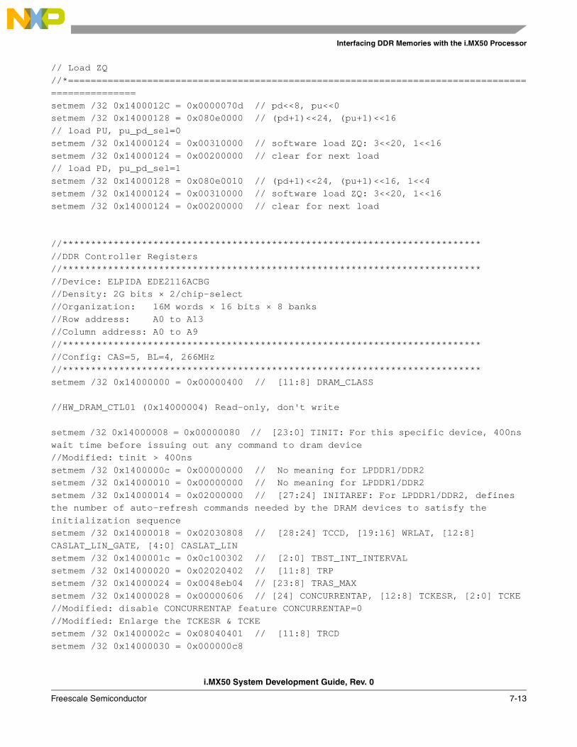
Interfacing DDR Memories with the i.MX50 Processor
i.MX50 System Development Guide, Rev. 0
Freescale Semiconductor 7-13
// Load ZQ//*================================================================================================setmem /32 0x1400012C = 0x0000070d // pd<<8, pu<<0setmem /32 0x14000128 = 0x080e0000 // (pd+1)<<24, (pu+1)<<16// load PU, pu_pd_sel=0setmem /32 0x14000124 = 0x00310000 // software load ZQ: 3<<20, 1<<16setmem /32 0x14000124 = 0x00200000 // clear for next load// load PD, pu_pd_sel=1setmem /32 0x14000128 = 0x080e0010 // (pd+1)<<24, (pu+1)<<16, 1<<4setmem /32 0x14000124 = 0x00310000 // software load ZQ: 3<<20, 1<<16setmem /32 0x14000124 = 0x00200000 // clear for next load
//**************************************************************************//DDR Controller Registers//**************************************************************************//Device: ELPIDA EDE2116ACBG//Density: 2G bits × 2/chip-select//Organization: 16M words × 16 bits × 8 banks//Row address: A0 to A13//Column address: A0 to A9//**************************************************************************//Config: CAS=5, BL=4, 266MHz//**************************************************************************setmem /32 0x14000000 = 0x00000400 // [11:8] DRAM_CLASS
//HW_DRAM_CTL01 (0x14000004) Read-only, don't write
setmem /32 0x14000008 = 0x00000080 // [23:0] TINIT: For this specific device, 400ns wait time before issuing out any command to dram device //Modified: tinit > 400nssetmem /32 0x1400000c = 0x00000000 // No meaning for LPDDR1/DDR2setmem /32 0x14000010 = 0x00000000 // No meaning for LPDDR1/DDR2setmem /32 0x14000014 = 0x02000000 // [27:24] INITAREF: For LPDDR1/DDR2, defines the number of auto-refresh commands needed by the DRAM devices to satisfy the initialization sequencesetmem /32 0x14000018 = 0x02030808 // [28:24] TCCD, [19:16] WRLAT, [12:8] CASLAT_LIN_GATE, [4:0] CASLAT_LINsetmem /32 0x1400001c = 0x0c100302 // [2:0] TBST_INT_INTERVALsetmem /32 0x14000020 = 0x02020402 // [11:8] TRPsetmem /32 0x14000024 = 0x0048eb04 // [23:8] TRAS_MAXsetmem /32 0x14000028 = 0x00000606 // [24] CONCURRENTAP, [12:8] TCKESR, [2:0] TCKE//Modified: disable CONCURRENTAP feature CONCURRENTAP=0//Modified: Enlarge the TCKESR & TCKEsetmem /32 0x1400002c = 0x08040401 // [11:8] TRCDsetmem /32 0x14000030 = 0x000000c8
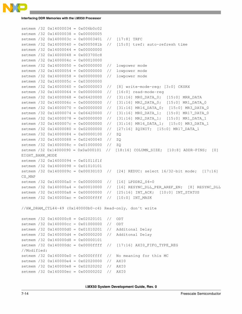
Interfacing DDR Memories with the i.MX50 Processor
i.MX50 System Development Guide, Rev. 0
7-14 Freescale Semiconductor
setmem /32 0x14000034 = 0x006b0c02setmem /32 0x14000038 = 0x00000005setmem /32 0x1400003c = 0x00003401 // [17:8] TRFCsetmem /32 0x14000040 = 0x0005081b // [15:0] tref: auto-refresh timesetmem /32 0x14000044 = 0x00000000setmem /32 0x14000048 = 0x003700c8setmem /32 0x1400004c = 0x00010000setmem /32 0x14000050 = 0x00000000 // lowpower modesetmem /32 0x14000054 = 0x00000000 // lowpower modesetmem /32 0x14000058 = 0x00000000 // lowpower modesetmem /32 0x1400005c = 0x03000000setmem /32 0x14000060 = 0x00000003 // [8] write-mode-reg; [3:0] CKSRXsetmem /32 0x14000064 = 0x00000000 // [16:0] read-mode-regsetmem /32 0x14000068 = 0x06420000 // [31:16] MR0_DATA_0; [15:0] MRR_DATAsetmem /32 0x1400006c = 0x00000000 // [31:16] MR2_DATA_0; [15:0] MR1_DATA_0setmem /32 0x14000070 = 0x00000000 // [31:16] MR16_DATA_0; [15:0] MR3_DATA_0setmem /32 0x14000074 = 0x06420000 // [31:16] MR0_DATA_1; [15:0] MR17_DATA_0setmem /32 0x14000078 = 0x00000000 // [31:16] MR2_DATA_1; [15:0] MR1_DATA_1setmem /32 0x1400007c = 0x00000000 // [31:16] MR16_DATA_1; [15:0] MR3_DATA_1setmem /32 0x14000080 = 0x02000000 // [27:16] ZQINIT; [15:0] MR17_DATA_1setmem /32 0x14000084 = 0x00000100 // ZQsetmem /32 0x14000088 = 0x02400040 // ZQsetmem /32 0x1400008c = 0x01000000 // ZQsetmem /32 0x14000090 = 0x0a000101 // [18:16] COLUMN_SIZE; [10:8] ADDR-PINS; [0] EIGHT_BANK_MODEsetmem /32 0x14000094 = 0x01011f1fsetmem /32 0x14000098 = 0x01010101setmem /32 0x1400009c = 0x00030103 // [24] REDUC: select 16/32-bit mode; [17:16] CS_MAPsetmem /32 0x140000a0 = 0x00000000 // [16] LPDDR2_S4=0setmem /32 0x140000a4 = 0x00010000 // [16] RESYNC_DLL_PER_AREF_EN; [8] RESYNC_DLLsetmem /32 0x140000a8 = 0x00000000 // [25:16] INT_ACK; [10:0] INT_STATUSsetmem /32 0x140000ac = 0x0000ffff // [10:0] INT_MASK
//HW_DRAM_CTL44~49 (0x140000b0~c4) Read-only, don't write
setmem /32 0x140000c8 = 0x02020101 // ODTsetmem /32 0x140000cc = 0x01000000 // ODTsetmem /32 0x140000d0 = 0x01010201 // Additonal Delaysetmem /32 0x140000d4 = 0x00000200 // Additonal Delaysetmem /32 0x140000d8 = 0x00000101setmem /32 0x140000dc = 0x0000ffff // [17:16] AXI0_FIFO_TYPE_REG//Modified: setmem /32 0x140000e0 = 0x0000ffff // No meaning for this MCsetmem /32 0x140000e4 = 0x02020000 // AXI0setmem /32 0x140000e8 = 0x02020202 // AXI0setmem /32 0x140000ec = 0x00000202 // AXI0
Interfacing DDR Memories with the i.MX50 Processor
i.MX50 System Development Guide, Rev. 0
Freescale Semiconductor 7-15
setmem /32 0x140000f0 = 0x01010064 // AXI1setmem /32 0x140000f4 = 0x01010101 // AXI1setmem /32 0x140000f8 = 0x00010101 // AXI0setmem /32 0x140000fc = 0x00000064 // [16] CKE_STATUSsetmem /32 0x14000100 = 0x00000000setmem /32 0x14000104 = 0x02000702 // DFIsetmem /32 0x14000108 = 0x081b0000 // DFIsetmem /32 0x1400010c = 0x081b081b // DFIsetmem /32 0x14000110 = 0x081b081b // DFIsetmem /32 0x14000114 = 0x0304081b // [27:24] WRLAT_ADJ; [20:16] RDLAT_ADJsetmem /32 0x14000118 = 0x00010002 // [24] ODT_ALT_EN=0//Modified: ODT_ALT_EN must be 0setmem /32 0x1400011c = 0x00001000 // [12] AXI0_HIDE_BRESP=1; [8] MDDR_CKE_SEL; [0] AXI0_AWCOBUF=0//Modified: Recommend AXI0_HIDE_BRESP = 1
//**************************************************************************//DDR PHY Registers//**************************************************************************setmem /32 0x14000200 = 0x00000000 // RESERVEDsetmem /32 0x14000204 = 0x00000000 // on-chip ODT//[26:24] RD_DLY_SEL; [15:12] DQS_OE_START; [11:8] DQS_OE_END; [6:4] DATA_OE_START; [2:0] DATA_OE_ENDsetmem /32 0x14000208 = 0x34013a27 // data-slice-0: PHY_CTRL_REG_0_B0setmem /32 0x14000210 = 0x34013a27 // data-slice-1: PHY_CTRL_REG_0_B1setmem /32 0x14000218 = 0x34013a27 // data-slice-2: PHY_CTRL_REG_0_B2setmem /32 0x14000220 = 0x34013a27 // data-slice-3: PHY_CTRL_REG_0_B3setmem /32 0x14000228 = 0x34013a27 // data-slice-CA: PHY_CTRL_REG_0_CA//[8:6] GATE_ERR_DELAY; [5:4] GATE_CLOSE_CFG; [2:0] GATE_CFGsetmem /32 0x1400020c = 0x26c002c0 // data-slice-0: PHY_CTRL_REG_1_B0setmem /32 0x14000214 = 0x26c002c0 // data-slice-1: PHY_CTRL_REG_1_B1setmem /32 0x1400021c = 0x26c002c0 // data-slice-2: PHY_CTRL_REG_1_B2setmem /32 0x14000224 = 0x26c002c0 // data-slice-3: PHY_CTRL_REG_1_B3setmem /32 0x1400022c = 0x26c002c0 // data-slice-CA: PHY_CTRL_REG_1_CAsetmem /32 0x14000230 = 0x00000000 // RESERVED//[23] DFI_MOBILE_EN=1; [16] DDR_SEL=1; [3:0] DFI_RDDATA_VALID >= RD_DLY_SEL + 1setmem /32 0x14000234 = 0x00000005 // PHY_CTRL_REG_2//[31:29] PHASE_DETECT_SEL; [28] DLL_BYPASS_MODE; [23:15] DLL_RD_DELAY_BYPASS; [14:8] DLL_RD_DELAY; [7:0] DLL_START_POINTsetmem /32 0x14000238 = 0x60101414 // data-slice-0: DLL_CTRL_REG_0_B0setmem /32 0x14000240 = 0x60101414 // data-slice-1: DLL_CTRL_REG_0_B1setmem /32 0x14000248 = 0x60101414 // data-slice-2: DLL_CTRL_REG_0_B2setmem /32 0x14000250 = 0x60101414 // data-slice-3: DLL_CTRL_REG_0_B3setmem /32 0x14000258 = 0x60101414 // data-slice-CA: DLL_CTRL_REG_0_CA//[23:15] DLL_WR_DELAY_BYPASS; [14:8] DLL_WR_DELAY; [7:0] DLL_INCRsetmem /32 0x1400023c = 0x00101401 // data-slice-0: DLL_CTRL_REG_1_B0

Interfacing DDR Memories with the i.MX50 Processor
i.MX50 System Development Guide, Rev. 0
7-16 Freescale Semiconductor
setmem /32 0x14000244 = 0x00101401 // data-slice-1: DLL_CTRL_REG_1_B1setmem /32 0x1400024c = 0x00101401 // data-slice-2: DLL_CTRL_REG_1_B2setmem /32 0x14000254 = 0x00101401 // data-slice-3: DLL_CTRL_REG_1_B3setmem /32 0x1400025c = 0x00101401 // data-slice-CA: DLL_CTRL_REG_1_CA
//*================================================================================================// Start ddr init sequence//*================================================================================================setmem /32 0x14000000 = 0x00000401 // bit[0]: start
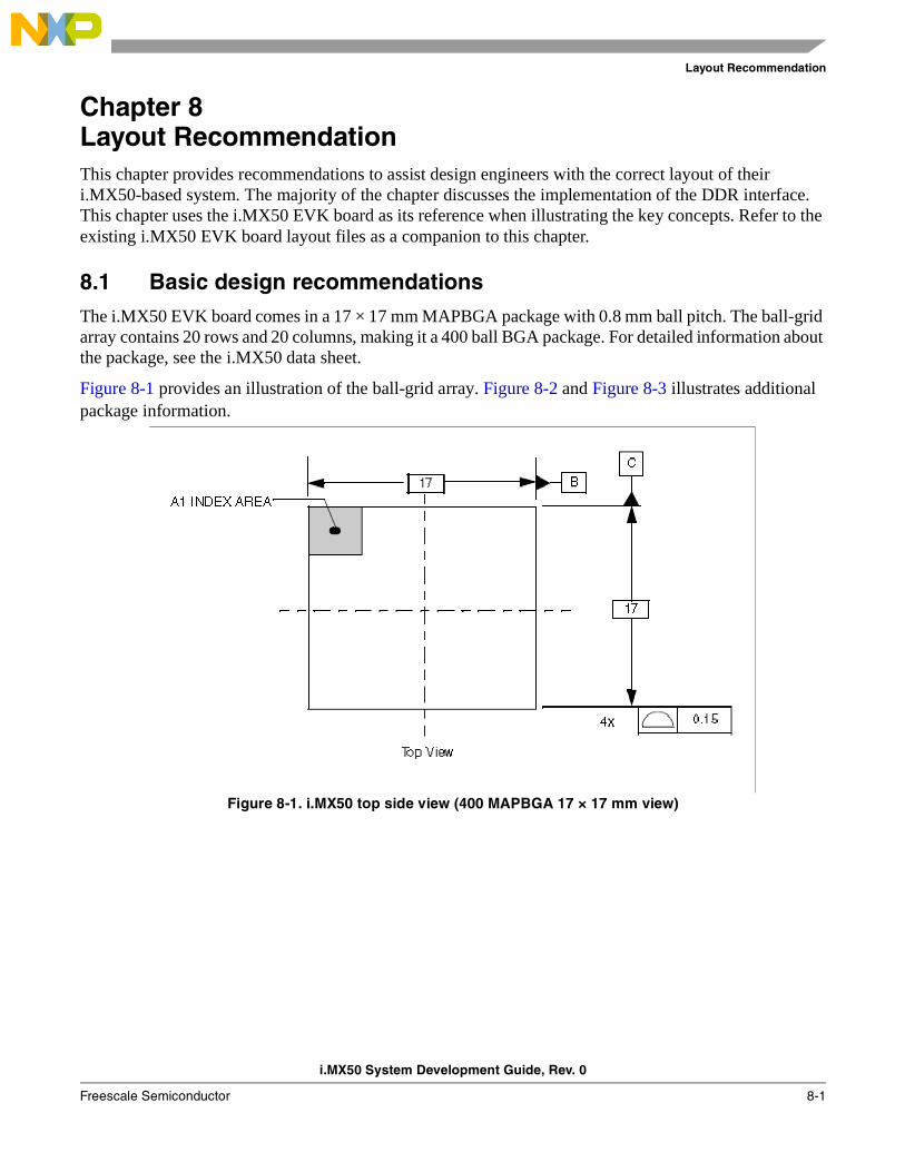
Layout Recommendation
i.MX50 System Development Guide, Rev. 0
Freescale Semiconductor 8-1
Chapter 8 Layout RecommendationThis chapter provides recommendations to assist design engineers with the correct layout of their i.MX50-based system. The majority of the chapter discusses the implementation of the DDR interface. This chapter uses the i.MX50 EVK board as its reference when illustrating the key concepts. Refer to the existing i.MX50 EVK board layout files as a companion to this chapter.
8.1 Basic design recommendationsThe i.MX50 EVK board comes in a 17 × 17 mm MAPBGA package with 0.8 mm ball pitch. The ball-grid array contains 20 rows and 20 columns, making it a 400 ball BGA package. For detailed information about the package, see the i.MX50 data sheet.
Figure 8-1 provides an illustration of the ball-grid array. Figure 8-2 and Figure 8-3 illustrates additional package information.
Figure 8-1. i.MX50 top side view (400 MAPBGA 17 × 17 mm view)
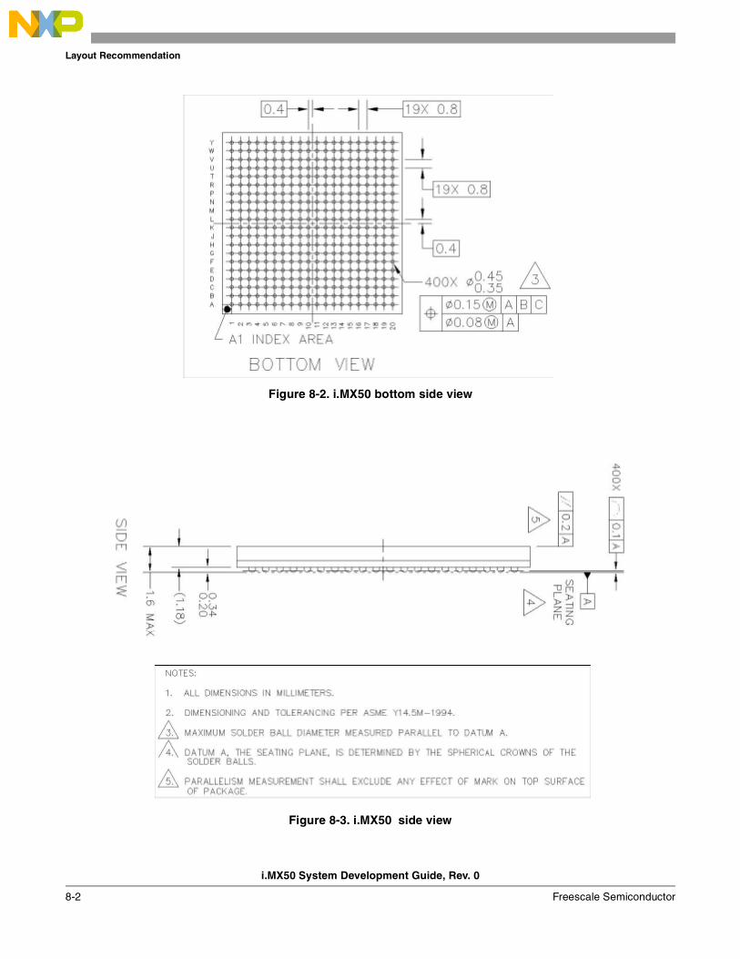
Layout Recommendation
i.MX50 System Development Guide, Rev. 0
8-2 Freescale Semiconductor
Figure 8-2. i.MX50 bottom side view
Figure 8-3. i.MX50 side view
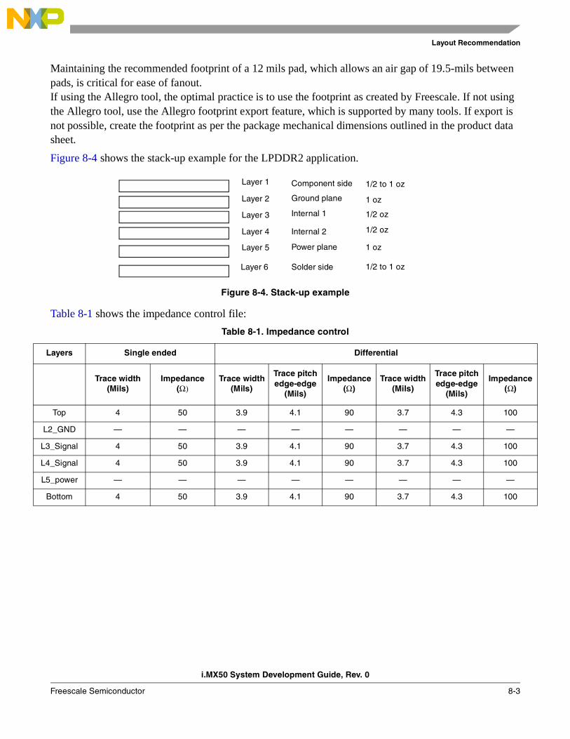
Layout Recommendation
i.MX50 System Development Guide, Rev. 0
Freescale Semiconductor 8-3
Maintaining the recommended footprint of a 12 mils pad, which allows an air gap of 19.5-mils between pads, is critical for ease of fanout.If using the Allegro tool, the optimal practice is to use the footprint as created by Freescale. If not using the Allegro tool, use the Allegro footprint export feature, which is supported by many tools. If export is not possible, create the footprint as per the package mechanical dimensions outlined in the product data sheet.
Figure 8-4 shows the stack-up example for the LPDDR2 application.
Figure 8-4. Stack-up example
Table 8-1 shows the impedance control file:
Table 8-1. Impedance control
Layers Single ended Differential
Trace width(Mils)
Impedance(Ω)
Trace width(Mils)
Trace pitch edge-edge
(Mils)
Impedance(Ω)
Trace width(Mils)
Trace pitch edge-edge
(Mils)
Impedance(Ω)
Top 4 50 3.9 4.1 90 3.7 4.3 100
L2_GND — — — — — — — —
L3_Signal 4 50 3.9 4.1 90 3.7 4.3 100
L4_Signal 4 50 3.9 4.1 90 3.7 4.3 100
L5_power — — — — — — — —
Bottom 4 50 3.9 4.1 90 3.7 4.3 100
Layer 1 Component side 1/2 to 1 oz
Layer 2
Layer 3
Layer 4
Layer 5
Layer 6
Ground plane
Internal 1
Internal 2
Power plane
Solder side
1 oz
1/2 oz
1/2 oz
1 oz
1/2 to 1 oz
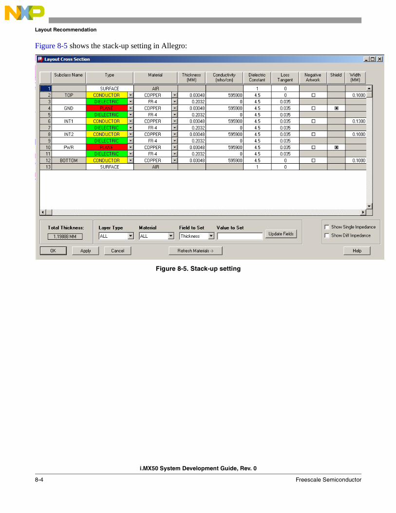
Layout Recommendation
i.MX50 System Development Guide, Rev. 0
8-4 Freescale Semiconductor
Figure 8-5 shows the stack-up setting in Allegro:
Figure 8-5. Stack-up setting
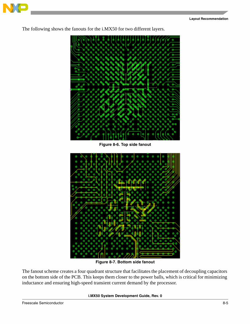
Layout Recommendation
i.MX50 System Development Guide, Rev. 0
Freescale Semiconductor 8-5
The following shows the fanouts for the i.MX50 for two different layers.
Figure 8-6. Top side fanout
Figure 8-7. Bottom side fanout
The fanout scheme creates a four quadrant structure that facilitates the placement of decoupling capacitors on the bottom side of the PCB. This keeps them closer to the power balls, which is critical for minimizing inductance and ensuring high-speed transient current demand by the processor.

Layout Recommendation
i.MX50 System Development Guide, Rev. 0
8-6 Freescale Semiconductor
A correct via size is critical for preserving adequate routing space. The recommended geometry for the via pads is: pad size 16 mils and drill 8 mils.
The constraints for the trace size may depend on a number of factors, such as the board stackup and associated di-electric and copper thickness, required impedance, and required current (for power traces).
On the Freescale reference design, the minimum trace width of 3 mils is used for the DDR routing.
8.2 DDR2 routing rulesDDR2 routing can be accomplished two different ways: routing all signals at the same length or routing by byte group.
Routing all signals at the same length can be more difficult at first because of the tight space between the DDR and the processor and the large number of required interconnects. However, it is the better way because it makes signal timing analysis straightforward. Table 8-2 explains how to route the signals by the same length.
Routing by byte group requires better control of the signals of each group. It is also a little more difficult for analysis and constraint settings. However, its advantage is that the constraint to match lengths can be applied to a smaller group of signals. This is often more achievable once the constraints are properly set. Table 8-3 explains how to route the signals by byte group.
Table 8-2. DDR2 routing by the same length
Signals Length Considerations
Address and bank Clock length Match the signals ± 25 mils of the value specified in the length column
Data and buffer Clock length
Control signals Clock length
Clock Lcritical (3 inches) Match the signals of clocks signals ± 5 mils.
DQS and DQS_B Clock length Match the signals of DQS signals ± 10 mils of the value specified in the length column.
Table 8-3. DDR2 routing by byte group
Signals GroupLength
ConsiderationsMin Max
DRAM_SDCLK[1:0]DRAM_SDCLK_B[1:0]
Clock Short as possible 2 inches Match the signals ± 5 mils.2 inches is recommended.
DRAM_A[15:0]DRAM_SDBA[2:0]
DRAM_RASDRAM_CAS
DRAM_SDWE
Address and Command
Clock (min) – 200 Clock (min) Match the signals ± 25 mils.

Layout Recommendation
i.MX50 System Development Guide, Rev. 0
Freescale Semiconductor 8-7
8.3 ESD and radiated emissions recommendationsThe PCB design should use 6 or more layers, with solid power and ground planes. The recommendations for ESD immunity and radiated emissions performance are:
• All components with ground chassis shields (such as USB jack and buttons) should connect the shield to the PCB chassis ground ring.
• Ferrite beads should be placed on each signal line connecting to an external cable. These ferrite beads must be placed as close to the PCB jack as possible.
NOTEFerrite beads should have a minimum impedance of 500 Ω at 100 MHz with the exception of the ferrite on USB_5V.
• Ferrite beads should NOT be placed on the USB D+/D– signal lines as this can cause USB signal integrity problems. For radiated emissions problems due to USB, a common mode choke may be placed on the D+/D– signal lines. However, it should not be required if the PCB layout is satisfactory. Ideally, the common mode choke should be approved for high speed USB use or tested thoroughly to verify that no signal integrity issues are created.
• It is highly recommended that ESD protection devices be used on ports connecting to external connectors. Refer to the reference schematic (available on the Freescale website) for detailed information about ESD protection implementation on the USB.
DRAM_D[7:0]DRAM_DQM0DRAM_SDQS0
DRAM_SDQS0_B
Byte Group 1 __ Clock (min) Match the signals of each byte group ± 25 mils.All byte groups (1 to 4) matched ± 50 milsMatch the differential signals of DQS ± 10 mils.
DRAM_D[15:8]DRAM_DQM1DRAM_SDQS1
DRAM_SDQS1_B
Byte Group 2 __ Clock (min)
DRAM_D[23:16]DRAM_DQM2DRAM_SDQS2
DRAM_SDQS2_B
Byte Group 3 __ Clock (min)
DRAM_D[31:24]DRAM_DQM3DRAM_SDQS3
DRAM_SDQS3_B
Byte Group 4 __ Clock (min)
DRAM_CS[1:0]DRAM_SDCKE[1:0]DRAM_SDODT[1:0]
Control signals Clock (min) – 200 Clock (min) Match the signals ± 50 mils.
Table 8-3. DDR2 routing by byte group (continued)
Signals GroupLength
ConsiderationsMin Max

Layout Recommendation
i.MX50 System Development Guide, Rev. 0
8-8 Freescale Semiconductor

i.MX50 System Development Guide, Rev. 0
Freescale Semiconductor -1
Part IISoftware DevelopmentThe chapters that follow aid you in software development for your product utilizing the i.MX50 Board Support Package.

i.MX50 System Development Guide, Rev. 0
Freescale Semiconductor 9-1
Chapter 9 Porting U-Boot from an i.MX50 Reference Board to an i.MX50 Custom BoardThis chapter provides a step-by-step guide that explains how to add i.MX50 custom board support to U-Boot. This developer's guide is based on U-Boot version rel_imx_2.6.35_11.04.01, which is present as a package on the LTIB-based Linux BSP at http://opensource.freescale.com/git?p=imx/uboot-imx.git.
For an introduction to the use of U-Boot firmware with i.MX processors, read AN4173, “U-Boot for i.MX51 Based Designs,” which is available on the Freescale website.
9.1 Obtaining the source code for the U-BootThe following steps explain how to obtain the source code.
1. Install LTIB as usual. Make sure you deselect U-Boot from compilation.
2. Manually unpack u-boot: ./ltib -m prep -p u-boot.
The U-Boot code is now located at rpm/BUILD/u-boot-<version number>. The guide will now refer to the U-Boot main directory as <UBOOT_DIR> and assumes that your shell working directory is <UBOOT_DIR>.
9.2 Preparing the codeThe following steps explain how to prepare the code.
1. Make a copy of the board directory, using the following instruction:$cp -R board/freescale/mx50_<reference board name> board/freescale/mx50_<custom board
name>
2. Copy the existing mx50_<reference board name>.h board configuration file as mx50_<custom board name>.h, using the following instruction.$cp include/configs/mx50_<reference board name>.h include/configs/mx50_<custom board
name>.h
3. Create one entry in <UBOOT_DIR>/Makefile for the new i.MX50-based configuration. This file is in alphabetical order. The instruction to use is as follows:mx50_<custom board name>_config : unconfig
@$(MKCONFIG) $(@:_config=) arm arm_cortexa8 mx50_<custom board name> freescale mx50

Porting U-Boot from an i.MX50 Reference Board to an i.MX50 Custom Board
i.MX50 System Development Guide, Rev. 0
9-2 Freescale Semiconductor
NOTEU-Boot project developers recommend adding any new board to the MAKEALL script and to run this script in order to validate that the new code has not broken any other’s platform build. This is a requirement if you plan to submit a patch back to the U-Boot community. For further information, consult the U-Boot README file.
4. Rename board/freescale/mx50_<custom board name>/mx50_<reference board name>.c as board/freescale/mx50_<custom board name>/mx50_<custom board name>.c.
5. Adapt any fixed paths. In this case, the linker script board/freescale/mx50_<custom board name>/u-boot.lds has at least two paths that must be changed
— Change board/freescale/mx50_<reference board name>/flash_header.o to board/freescale/mx50_<custom board name>/flash_header.o
— Change board/freescale/mx50_<reference board name>/libmx50_<reference board name>.a to board/freescale/mx50_<custom board name>/libmx50_<custom board name>.a
6. Change the line COBJS := mx50_<reference board name>.o (inside board/freescale/mx50_<custom board name>/Makefile) to COBJS := mx50_<custom board name>.o
NOTEThe remaining instructions build the U-Boot manually and do not use LTIB.
7. Create a shell script under <UBOOT_DIR> named build_u-boot.sh.
The file’s contents are now:#!/bin/bashexport ARCH=armexport CROSS_COMPILE=<path to cross compiler/prefix> (e.g. PATH:/opt/freescale/usr/local/gcc-4.4.4-glibc-2.11.1-multilib-1.0/arm-fsl-linux-gnueabi/bin/arm-none-linux-gnueabi-export PATH=$PATH:<path to compiler>
make mx50_<custom board name>_configmake
8. Compile U-Boot using $./build_u-boot.sh
9. If everything is correct, you should see the file u-boot.bin as proof that your build setup is correct and ready to be customized.
The new i.MX50 custom board that you have created is an exact copy of the i.MX50 reference board, but the boards are two independent builds. This allows you to proceed to the next step: customizing the code to suit the new hardware design.
9.3 Customizing the i.MX50 custom board codeThe new i.MX50 custom board is part of the U-Boot source tree, but it is a duplicate of the i.MX50 reference board code and needs to be customized.
The DDR technology is a potential key difference between the two boards. If there is a difference in the DDR technology between the two boards, the DDR initialization needs to be ported. DDR initialization is

Porting U-Boot from an i.MX50 Reference Board to an i.MX50 Custom Board
i.MX50 System Development Guide, Rev. 0
Freescale Semiconductor 9-3
coded in the plug-in code, inside the boot header of the U-Boot image. When porting bootloader, kernel or driver code, you must have the schematics easily accessible for reference.
9.3.1 Changing DRAM values for i.MX50 with LP-DDR2 initialization
Initializing the memory interface requires configuring the relevant I/O pins with the right mode and impedance and initializing the DATABAHN module.
1. To port to the custom board, the appropriate DDR initialization needs to be used. This is the same initialization as would be used in a JTAG initialization script.
2. Open the file board/freescale/mx50_<custom board name>/flash_header.S
3. Modify the required IOMUX register values with the right mode and impedance values
4. Modify the DDR settings to match the memory specifications, no need to modify the do_zq_calib macro routine
This is the new board/freescale/mx50_<custom board name>/flash_header.S customized for LP-DDR2.
9.3.2 Booting with the modified U-Boot
If the plug-in code (board/freescale/mx50_<custom board name>/flash_header.S) was modified successfully, you can compile and write u-boot.bin to an SD card. To test this, insert the SD card into the SD card socket of the CPU board and power cycle the board.
A message like this should be printed in the console:U-Boot 2009.08 (Jul 29 2010 - 15:17:24) CPU: Freescale i.MX50 family 1.0V at 800 MHz Board: Unkown board id1:11 Boot Reason: [POR] Boot Device: SD I2C: ready DRAM: 1 GB MMC: FSL_ESDHC: 0, FSL_ESDHC: 1 Card did not respond to voltage select! MMC init failed In: serial Out: serial Err: serial Net: FEC0 <reference board name>: U-Boot >
9.3.3 Further customization at system boot
To further customize your U-Boot board project, use the first function that system boot calls on:start_armboot in "lib_arm/board.c".board_init()
All board initialization is executed inside this function. It starts by running through the init_sequence[] array of function pointers.
Porting U-Boot from an i.MX50 Reference Board to an i.MX50 Custom Board
i.MX50 System Development Guide, Rev. 0
9-4 Freescale Semiconductor
The first board dependent function inside init_sequence[] array is board_init(). board_init() is implemented inside board/freescale/mx50_<custom board name>.c.
At this point the most important tip is the following line of code:...
gd->bd->bi_arch_number = MACH_TYPE_MX50_<reference board name>; /* board id for Linux */
...
To customize your board ID, go to the registration process at http://www.arm.linux.org.uk/developer/machines/
This tutorial will continue to use MACH_TYPE_MX50_<reference board name>.
9.3.4 Customizing the printed board name
To customize the printed board name, use the checkboard() function. This function is called from the init_sequence[] array implemented inside board/freescale/mx50_<custom board name>.c. There are two ways to use checkboard() to customize the printed board name from Board: Unknown board id1:11 to Board: MX50 CPU3 on <custom board name>2: the brute force way or by using a more flexible identification method if implemented on the custom board.
To customize the brute force way, inside checkboard() and replace printf("Board: "); with printf("Board: MX50 CPU3 on <custom board>\n");
Alternatively, if the custom board provides a method to detect the board type via an external signal this can be detected in the checkboard() function and the according information is printed.
Once this has been done, recompile U-Boot and deploy u-boot.bin to the SD card. The new prompt message should be as follows:
U-Boot 2009.08 (Jul 30 2010 - 14:44:00) CPU: Freescale i.MX50 family 1.0V at 800 MHz Board: MX50 CPU3 on <custom board name> Boot Reason: [POR] Boot Device: SD I2C: ready DRAM: 1 GB MMC: FSL_ESDHC: 0, FSL_ESDHC: 1 Card did not respond to voltage select! MMC init failed In: serial Out: serial Err: serial Net: FEC0 Reference Board: U-Boot >
i.MX50 System Development Guide, Rev. 0
Freescale Semiconductor 10-1
Chapter 10 Porting the Android KernelAndroid releases for the i.MX50 processor are divided into three main parts: the bootloader (U-Boot or redboot), the kernel, and the Android framework. This chapter explains how to port an Android kernel to any platform that is based on the i.MX50 chip. The easiest way to apply kernel modifications to any i.MX platform is to use an existing Android release either for the i.MX50 or i.MX53 processor. See the i.MX Android-rx user guide (where rx stands for the release version) inside the Freescale Android release package for further details.
10.1 Patching the Android kernelBefore configuring the Android kernel, locate the BSP patches in the imx-android-rx folder, where x stands for the release version. This folder contains all BSP patches needed for the different i.MX platforms. It also contains patches for some of the libraries implemented on the hardware abstraction layer. Apply the relevant patches to the kernel.
10.2 Configuring Android release for customized platformsOnce the patches have been applied to the kernel, go to myandroid/kernel_imx/. Use the command make imx5_android_defconfig to prepare the configuration for your platform.
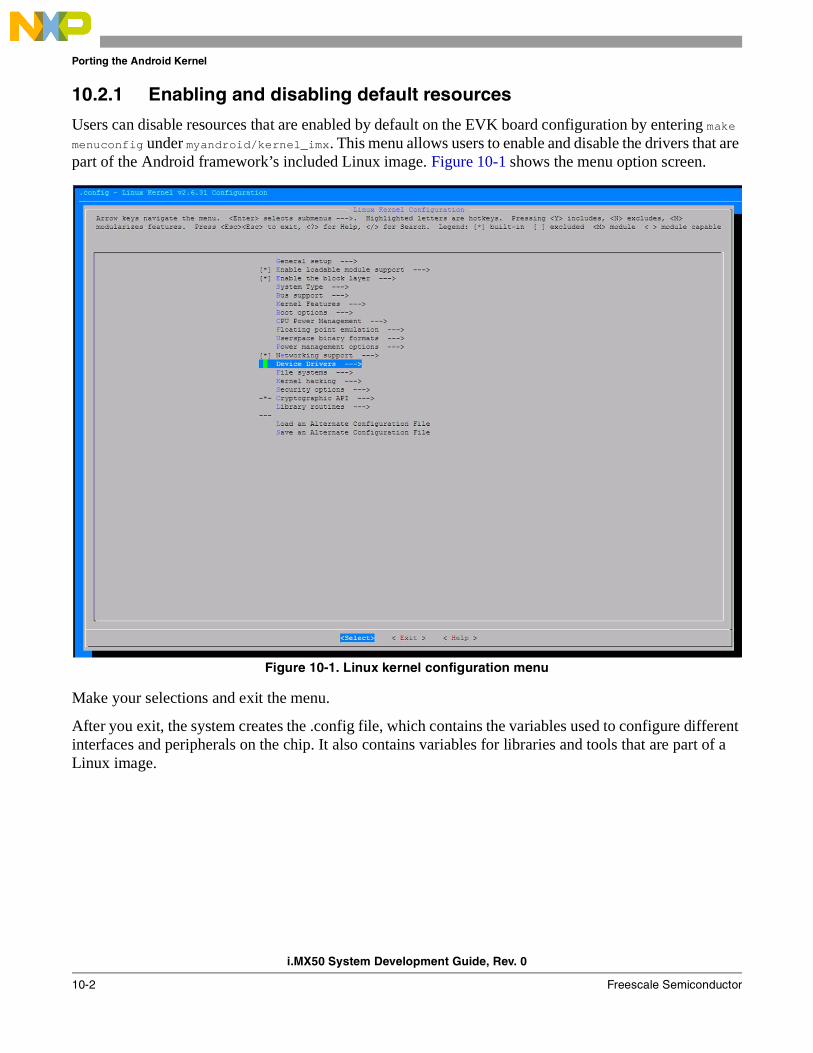
Porting the Android Kernel
i.MX50 System Development Guide, Rev. 0
10-2 Freescale Semiconductor
10.2.1 Enabling and disabling default resources
Users can disable resources that are enabled by default on the EVK board configuration by entering make menuconfig under myandroid/kernel_imx. This menu allows users to enable and disable the drivers that are part of the Android framework’s included Linux image. Figure 10-1 shows the menu option screen.
Figure 10-1. Linux kernel configuration menu
Make your selections and exit the menu.
After you exit, the system creates the .config file, which contains the variables used to configure different interfaces and peripherals on the chip. It also contains variables for libraries and tools that are part of a Linux image.
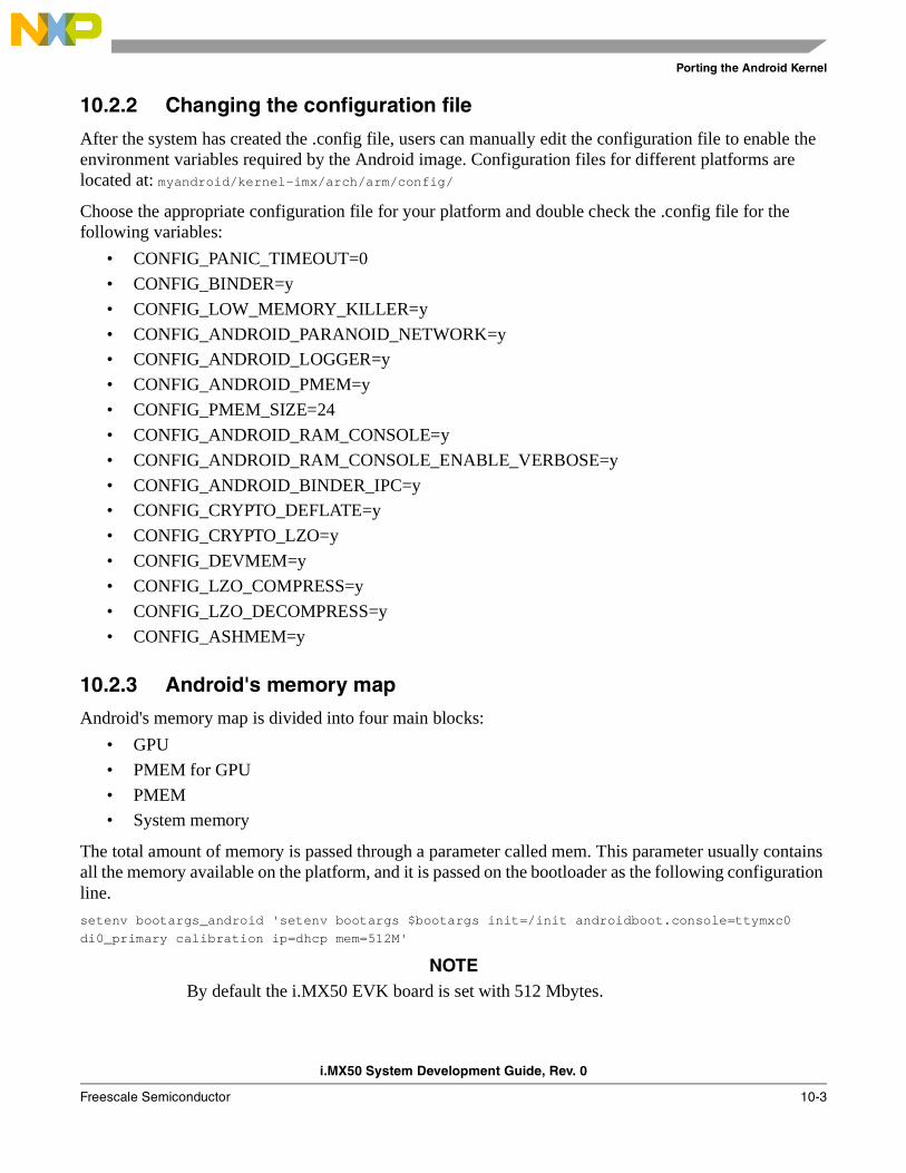
Porting the Android Kernel
i.MX50 System Development Guide, Rev. 0
Freescale Semiconductor 10-3
10.2.2 Changing the configuration file
After the system has created the .config file, users can manually edit the configuration file to enable the environment variables required by the Android image. Configuration files for different platforms are located at: myandroid/kernel-imx/arch/arm/config/
Choose the appropriate configuration file for your platform and double check the .config file for the following variables:
• CONFIG_PANIC_TIMEOUT=0
• CONFIG_BINDER=y
• CONFIG_LOW_MEMORY_KILLER=y
• CONFIG_ANDROID_PARANOID_NETWORK=y
• CONFIG_ANDROID_LOGGER=y
• CONFIG_ANDROID_PMEM=y
• CONFIG_PMEM_SIZE=24
• CONFIG_ANDROID_RAM_CONSOLE=y
• CONFIG_ANDROID_RAM_CONSOLE_ENABLE_VERBOSE=y
• CONFIG_ANDROID_BINDER_IPC=y
• CONFIG_CRYPTO_DEFLATE=y
• CONFIG_CRYPTO_LZO=y
• CONFIG_DEVMEM=y
• CONFIG_LZO_COMPRESS=y
• CONFIG_LZO_DECOMPRESS=y
• CONFIG_ASHMEM=y
10.2.3 Android's memory map
Android's memory map is divided into four main blocks:
• GPU
• PMEM for GPU
• PMEM
• System memory
The total amount of memory is passed through a parameter called mem. This parameter usually contains all the memory available on the platform, and it is passed on the bootloader as the following configuration line.
setenv bootargs_android 'setenv bootargs $bootargs init=/init androidboot.console=ttymxc0 di0_primary calibration ip=dhcp mem=512M'
NOTEBy default the i.MX50 EVK board is set with 512 Mbytes.
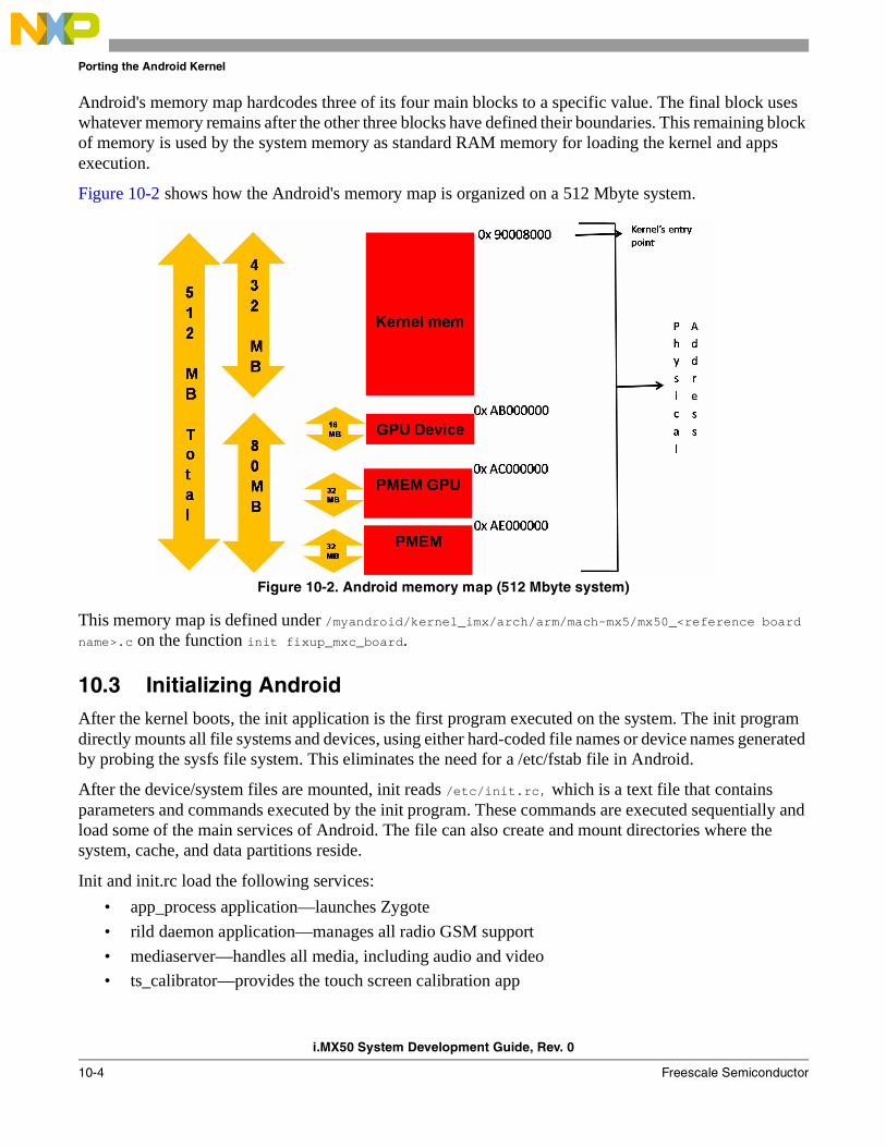
Porting the Android Kernel
i.MX50 System Development Guide, Rev. 0
10-4 Freescale Semiconductor
Android's memory map hardcodes three of its four main blocks to a specific value. The final block uses whatever memory remains after the other three blocks have defined their boundaries. This remaining block of memory is used by the system memory as standard RAM memory for loading the kernel and apps execution.
Figure 10-2 shows how the Android's memory map is organized on a 512 Mbyte system.
Figure 10-2. Android memory map (512 Mbyte system)
This memory map is defined under /myandroid/kernel_imx/arch/arm/mach-mx5/mx50_<reference board name>.c on the function init fixup_mxc_board.
10.3 Initializing AndroidAfter the kernel boots, the init application is the first program executed on the system. The init program directly mounts all file systems and devices, using either hard-coded file names or device names generated by probing the sysfs file system. This eliminates the need for a /etc/fstab file in Android.
After the device/system files are mounted, init reads /etc/init.rc, which is a text file that contains parameters and commands executed by the init program. These commands are executed sequentially and load some of the main services of Android. The file can also create and mount directories where the system, cache, and data partitions reside.
Init and init.rc load the following services:
• app_process application—launches Zygote
• rild daemon application—manages all radio GSM support
• mediaserver—handles all media, including audio and video
• ts_calibrator—provides the touch screen calibration app
Porting the Android Kernel
i.MX50 System Development Guide, Rev. 0
Freescale Semiconductor 10-5
10.4 Modifying the init.rc partition locationsThe init.rc file mounts the three main partitions—system, cache, and data—on the image. By default, these partitions are mounted from the SD/MMC controller.
If you have these partitions stored on another Flash source, modify the following lines to choose from the specific NVM.
• To mount the /system directory:mount ext3 /dev/block/mmcblk0p2 /systemmount ext3 /dev/block/mmcblk0p2 /system ro remount
• To mount the /data directory:mount ext3 /dev/block/mmcblk0p5 /data nosuid nodev
• To mounts the /recovery directory:mount ext3 /dev/block/mmcblk0p6 /cache nosuid nodev
You also can modify the partition number where the directories and files are stored.
10.5 Android enhancements to the Linux kernelMost Android porting is performed on the kernel side, as shown in Figure 10-3.
Figure 10-3. Linux kernel
By patching the Android kernel, Android adds enhancements to the Linux kernel in order to give upper layers services like interprocess communication and power management policies. Table 10-1 shows the enhancements.
Table 10-1. Android enhancements
Enhancement Purpose
Alarm Provide timers functionality to wake up and sleep the device
Ashmem Asynchronous shared memory share memory across process.
Binder Ipc binder driver for interprocess communication
Power Management New stack power management to increase performance
Low Memory Killer Provides the functionality for android memory management
Kernel Debugger Debug purposes
Logger Debug purposes
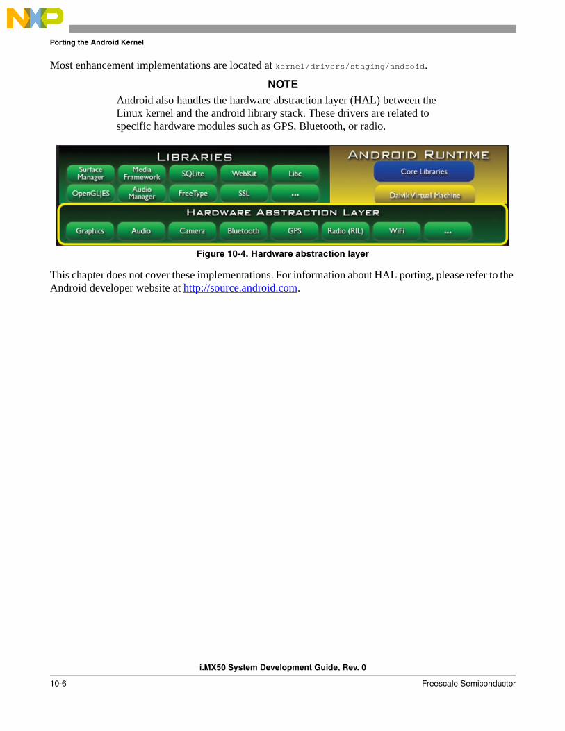
Porting the Android Kernel
i.MX50 System Development Guide, Rev. 0
10-6 Freescale Semiconductor
Most enhancement implementations are located at kernel/drivers/staging/android.
NOTEAndroid also handles the hardware abstraction layer (HAL) between the Linux kernel and the android library stack. These drivers are related to specific hardware modules such as GPS, Bluetooth, or radio.
Figure 10-4. Hardware abstraction layer
This chapter does not cover these implementations. For information about HAL porting, please refer to the Android developer website at http://source.android.com.

i.MX50 System Development Guide, Rev. 0
Freescale Semiconductor 11-1
Chapter 11 Porting the On-Board-Diagnostic-Suite (OBDS) to a Custom BoardThe on-board diagnostic suite (OBDS) is a set of validation software used during the board bring up phase and to validate the boards produced during mass manufacturing for defects. OBDS is run to test out specific IP blocks of the i.MX50 SoC and the associated hardware on the board.
In a typical scenario, a basic set of the hardware components are tested to be functional, prior to engaging the software team to bring up the bootloader and the BSP.
Prior to reading this document, be familiar with the following chapters in the i.MX50 Applications Processor Reference Manual:
• Chapter 1, “Introduction”
• Chapter 4, “External Signals and Pin Multiplexing”
• Chapter 5, “Clock Control Module (CCM)”
• Chapter 7, “System Debug”
• Chapter 35, “IOMUX Controller (IOMUX)”
11.1 Supported componentsThe OBDS package for Freescale’s i.MX50 reference board provides support for the following SoC internal functional blocks and hardware on the reference board:
• Debug UART test (used for communication with the host PC)
• DDR test
• Audio Out test
• LCD display test
• EINK display test
• I2C peripheral connectivity test
• MMC/SD test for SD Slot 2, where SD Slot 1 is implicitly tested as OBDS boots from SD1
• SRTC test
• Ethernet loopback test
• SPI-NOR test
• USBH1 device enumeration test
• NAND Flash device ID test
Porting the On-Board-Diagnostic-Suite (OBDS) to a Custom Board
i.MX50 System Development Guide, Rev. 0
11-2 Freescale Semiconductor
11.2 Customizing OBDS for specific hardwareThis section explains how to customize the OBDS for the following hardware modules:
• Section 11.2.1, “UART (serial port) test”
• Section 11.2.2, “DDR test”
• Section 11.2.3, “Audio test”
• Section 11.2.4, “LCD display test
• Section 11.2.5, “E-INK display test
• Section 11.2.6, “I2C test”
• Section 11.2.7, “SD/MMC test”
• Section 11.2.8, “SRTC test
• Section 11.2.9, “Ethernet (FEC) loopback test”
• Section 11.2.10, “SPI-NOR test”
• Section 11.2.11, “NAND Flash device ID test
11.2.1 UART (serial port) test
The UART port is the primary communications channel between the reference board and host PC. The UART test tests the transmission capabilities of the serial port and verifies its receive capabilities by prompting the user to input a character from the host PC to the serial port. Typing the character “X” exits this test and moves to the next test.
On the i.MX50 reference board, the UART1 TXD and RXD pins are routed to the UART1_TXD and UART1_RXD pins via the IOMUX (see the ~/diag-obds/src/mx50/hardware.c file). In addition, the file ~/diag-obds/src/mx50/mx50.c defines the debug_uart variable to UART1 (as seen below):
static struct hw_module *debug_uart = &uart1;
If a different UART port is used, make the required IOMUX changes to the routine debug_uart_iomux() function found in ~/diag-obds/src/mx50/hardware.c and update the debug_uart variable: void debug_uart_iomux(void){ //UART1//TXDwritel(ALT0, IOMUXC_SW_MUX_CTL_PAD_UART1_TXD);writel(0xE4, IOMUXC_SW_PAD_CTL_PAD_UART1_TXD);writel(0x0, IOMUXC_SW_PAD_CTL_GRP_UART);//RXDwritel(ALT0, IOMUXC_SW_MUX_CTL_PAD_UART1_RXD);writel(0xE4, IOMUXC_SW_PAD_CTL_PAD_UART1_RXD);writel(0x1, IOMUXC_UART1_IPP_UART_RXD_MUX_SELECT_INPUT);}
11.2.2 DDR test
The DDR test verifies the interface connectivity between the i.MX50 and the DDR memory. This test should not be confused with a stress test that validates robust signal integrity of the interface. Instead, this

Porting the On-Board-Diagnostic-Suite (OBDS) to a Custom Board
i.MX50 System Development Guide, Rev. 0
Freescale Semiconductor 11-3
test ensures the proper assembly of the memory and i.MX50 by testing for opens and shorts on the interface.
Each type of i.MX50 reference boards uses a different DDR configuration. If the custom board implements a DDR that has a different configuration than the reference boards, refer to the data sheet of the specific DDR and make the necessary changes to the DDR configurations in the ~/diag-obds/src/include/mx50/plat_startup.h file. This file sets up the IOMUX and DDR specific configurations.
11.2.3 Audio test
The audio test first performs I2C communications between the i.MX50 and the SGTL5000 audio codec. The test then outputs audio data via the SSI/I2S interface to the audio codec. The ~/diag-obds/src/drivers/audio folder contains the files that implement the audio test.
If a different SSI port and I2C port is used, make the necessary IOMUX changes to the ~/diag-obds/src/mx50/hardware.c file.
11.2.4 LCD display test
This test outputs an image to the 4.3” WVGA LCD Display.
Refer to the hardware.c file for changes in IOMUX when different pins are used to interface with the LCD panel. The code in the ~/diag-obds/src/drivers/lcdc/mxc_lcdc.c file has details on implementation of this test. The display’s data sheet provides the information for the different parameters.
11.2.5 E-INK display test
This test outputs an image to the E-INK display.
Refer to the hardware.c file for changes in IOMUX when different pins are used to interface with the E-INK panel. The code in the ~/diag-obds/src/drivers/epd folder contains the files that implement this test.
11.2.6 I2C test
This tests performs an I2C communications test with one or more devices on the I2C bus (reads back the device ID). ~/diag-obds/src/drivers/i2c folder contains the driver for the I2C module. Refer to hardware.c for I2C IOMUX setup. The test code to communicate with the different I2C devices can be found at ~/diag-obds/src/mx50/i2c_dev_tests.c
If another I2C port is needed, add a new entry for the other I2C IOMUX settings at hardware.c and change the I2C device test code depending on the I2C devices on the custom board.
Porting the On-Board-Diagnostic-Suite (OBDS) to a Custom Board
i.MX50 System Development Guide, Rev. 0
11-4 Freescale Semiconductor
11.2.7 SD/MMC test
This test performs a read/write test to the MMC/SD card plugged into the SD slot. This test configures and uses the ESDHCV2-2 module on the i.MX50 reference boards. The ~/diag-obds/src/drivers/mmc_sd/imx_mmc folder contains the files necessary to test the MMC/SD port.
Refer to the ~/diag-obds/src/mx50/hardware.c file for changes in IOMUX when a different ESDHC module is used to interface with the SD slot or if different pins are used than the ones used in the i.MX50 reference design.
11.2.8 SRTC test
This test ensures that the SRTC low power and high power domain counters are running. The test details can be found at the ~/diag-obds/src/drivers/timer/imx_timer folder.
11.2.9 Ethernet (FEC) loopback test
The test requires a loopback Ethernet cable. There is only one FEC in the i.MX50 SoC. Refer to the hardware.c file for changes in IOMUX in case pins other than the i.MX50 reference design are used to interface with the network interface.
11.2.10 SPI-NOR test
This test verifies the interface between the i.MX50 CSPI module and the SPI-NOR flash. The ~/diag-obds/src/drivers/spinor folder contains the files necessary to test the SPI-NOR Flash available on the i.MX50 reference board, using the i.MX50 CSPI module and CSPI SS1. Change ~/diag-obds/src/drivers/spinor/imx_spi_nor.c when using a different SPI-NOR device. See the following example implementation for the Atmel AT45DB321D SPI-NOR Flash.struct chip_id AT45DB321D_id ={ .id0 = 0x01, // Atmel AT45DB321D .id1 = 0x27, .id2 = 0x1f } The following calls are specific to the Atmel Flash:
• spi_nor_status_atmel
• spi_nor_write_atmel
If another ECSPI port is used to connect to the SPI-NOR (for example when connecting the SPI-NOR to ECSPI-1), make the following changes:
1. Inside ~/diag-obds/src/mx50/mx50.c, edit the code as shown in the bullet list below: platform_init(){...imx_spi_nor.base = CSPI1_BASE_ADDR;imx_spi_nor.freq = 25000000;imx_spi_nor.ss_pol = IMX_SPI_ACTIVE_LOW;imx_spi_nor.ss = 1;imx_spi_nor.fifo_sz = 32;imx_spi_nor.us_delay = 0;

Porting the On-Board-Diagnostic-Suite (OBDS) to a Custom Board
i.MX50 System Development Guide, Rev. 0
Freescale Semiconductor 11-5
spi_init_flash = imx_cspi_init;spi_xfer_flash = imx_cspi_xfer;...}
change the following:
— CSPI1_BASE_ADDR to ECSPI1_BASE_ADDR
— imx_cspi_init to imx_ecspi_init
— imx_cspi_xfer to imx_ecspi_xfer.
2. Add changes to the IOMUX settings for the other CSPI ports in ~/diag-obds/src/mx50/hardware.c.
11.2.11 NAND Flash device ID test
This test reads the NAND device’s ID and compares it to a list of NAND device IDs maintained inside ~/diag-obds/src/drivers/nand/supported_nand_parts.inl. If the test finds an unrecognized NAND ID, it prints that ID and asks the user to confirm it from the NAND device’s data sheet. ~/diag-obds/src/drivers/nand/stmp_nand contains the driver for the NAND module.
Refer to ~/diag-obds/src/mx50/hardware.c for changes in IOMUX if pins are used to interface with the NAND device other than the ones used in the i.MX50 reference design.

Porting the On-Board-Diagnostic-Suite (OBDS) to a Custom Board
i.MX50 System Development Guide, Rev. 0
11-6 Freescale Semiconductor
i.MX50 System Development Guide, Rev. 0
Freescale Semiconductor 12-1
Chapter 12 Configuring the IOMUX Controller (IOMUXC)Before using the i.MX50 pins (or pads), users must select the desired function and correct values for characteristics such as voltage level, drive strength, and hysteresis. They do this by configuring a set of registers from the IOMUXC.
For detailed information about each pin, see the “External Signals and Pin Multiplexing” chapter in the i.MX50 Applications Processor Reference Manual. For additional information about the IOMUXC block, see the “IOMUX Controller (IOMUXC)” chapter in the i.MX50 Applications Processor Reference Manual.
12.1 Information for setting IOMUX controller registersThe IOMUX controller contains four sets of registers that affect the i.MX50 registers, as follows:
• General-purpose registers (IOMUXC_GPRx)—consist of three registers that control PLL frequency, voltage, and other general purpose sets.
• “Daisy Chain” control registers (IOMUXC_<Instance_port>_SELECT_INPUT)—control the input path to a module when more than one pad may drive the module’s input
• MUX control registers (changing pad modes):
— Select which of the pad’s 8 different functions (also called ALT modes) is used.
— Can set pad’s functions individually or by group using one of the following registers:
– IOMUXC_SW_MUX_CTL_PAD_<PAD NAME>
– IOMUXC_SW_MUX_CTL_GRP_<GROUP NAME>
• Pad control registers (changing pad characteristics):
— Set pad characteristics individually or by group using one of the following registers:
– IOMUXC_SW_PAD_CTL_PAD_<PAD_NAME>
– IOMUXC_SW_PAD_CTL_GRP_<GROUP NAME>
— Pad characteristics are:
– SRE (1 bit slew rate control)—Slew rate control bit; selects between FAST/SLOW slew rate output. Fast slew rate is used for high frequency designs.
– DSE (2 bits drive strength control)—Drive strength control bits; select the drive strength (low, medium, high, or max).
– ODE (1 bit open drain control)—Open drain enable bit; selects open drain or CMOS output.
– HYS (1 bit hysteresis control)—Selects between CMOS or Schmitt Trigger when pad is an input.

Configuring the IOMUX Controller (IOMUXC)
i.MX50 System Development Guide, Rev. 0
12-2 Freescale Semiconductor
– PUS (2 bits pull up/down configuration value)—Selects between pull up or down and its value.
– PUE (1 bit pull/keep select)—Selects between pull up or keeper. A keeper circuit help assure that a pin stays in the last logic state when the pin is no longer being driven.
– PKE (1 bit enable/disable pull up, pull down or keeper capability)—Enable or disable pull up, pull down, or keeper.
– DDR_MODE_SEL (1 bit ddr_mode control)—Needed when interfacing DDR memories.
– DDR_INPUT (1 bit ddr_input control)—Needed when interfacing DDR memories.
12.2 Setting up the IOMUXC in U-BootTo set up the IOMUXC and configure the pads on U-Boot, use the four files described in Table 12-1:
12.2.1 Defining the pads
The iomux.c file contains each pad’s IOMUXC definitions. Use the following code to see the default definitions:
enum iomux_pins {.........MX50_PIN_KEY_COL0 = _MXC_BUILD_GPIO_PIN(3, 6, 1, 0x24, 0x34C),MX50_PIN_KEY_ROW0 = _MXC_BUILD_GPIO_PIN(3, 7, 1, 0x28, 0x350),.........}
To change the values for each pad according to your hardware configuration, use the following:MX50_PIN_<PIN NAME> = _MXC_BUILD_GPIO_PIN(gp, gi, ga, mi, pi)
Where:
• gp—IO Pin
• gi—IO Instance
• ga—MUX Mode
• mi—MUX Control Offset
Table 12-1. Configuration files
Path Filename Description
cpu/arm_cortexa8/mx50/ iomux.c Iomux functions (no need to change)
include/asm-arm/arch-mx50/ iomux.h Iomux definitions (no need to change)
include/asm-arm/arch-mx50/ mx50_pins.h Definition of all processor's pads
board/freescale/mx50_<reference board name>/ mx50_<reference board name>.c
Board initialization file
Configuring the IOMUX Controller (IOMUXC)
i.MX50 System Development Guide, Rev. 0
Freescale Semiconductor 12-3
• pi—PAD Control Offset
12.2.2 Configuring IOMUX pins for initialization function
The mx50_<reference board name>.c file contains the initialization functions for all peripherals (such as UART, I2C, and Ethernet). Configure the relevant pins for each initializing function, using the following:mxc_request_iomux(<pin name>, <iomux config>);mxc_iomux_set_input(<mux input select>, <mux input config>);mxc_iomux_set_pad(<pin name>, <iomux pad config>);
Where the following applies:
<pin name> See all pins definitions on file mx50_pins.h
<iomux config> See parameters defined at iomux_config enumeration on file iomux.h
<iomux input select> See parameters defined at iomux_input_select enumeration on file iomux.h
<iomux input config> See parameters defined at iomux_input_config enumeration on file iomux.h
<iomux pad config> See parameters defined at iomux_pad_config enumeration on file iomux.h
12.2.3 Example—setting a GPIO
For an example, configure and use pin PATA_DA_1 (PIN L3) as a general GPIO and toggle its signal.
Add the following code to the file mx50_<reference board name>.c, function board_init:
// Request ownership for an IO pin.mxc_request_iomux(MX50_PIN_ECSPI1_SCLK, IOMUX_CONFIG_ALT1);
// Set pin as 0reg = readl(GPIO4_BASE_ADDR + 0x0);reg &= ~0x80;writel(reg, GPIO4_BASE_ADDR + 0x0);
// Set pin direction as outputreg = readl(GPIO4_BASE_ADDR + 0x4);reg |= 0x80;writel(reg, GPIO4_BASE_ADDR + 0x4);
// Delay 0.5 secondsudelay(500000);
// Set pin as 1reg = readl(GPIO4_BASE_ADDR + 0x0);reg |= 0x80;writel(reg, GPIO4_BASE_ADDR + 0x0);
// Delay 0.5 secondsudelay(500000);
Configuring the IOMUX Controller (IOMUXC)
i.MX50 System Development Guide, Rev. 0
12-4 Freescale Semiconductor
// Set pin as 0reg = readl(GPIO7_BASE_ADDR + 0x0);reg &= ~0x80;writel(reg, GPIO7_BASE_ADDR + 0x0);
If done correctly, the pin ECSPI_SCLK on the i.MX50 toggles when booting.
12.3 Setting up the IOMUXC in LinuxThe folder linux/arch/arm/mach-<platform name> contains the specific machine layer file for your custom board. For example, the machine layer file used on the i.MX50 <reference> boards are linux/arch/arm/mach-mx5/mx50_<reference board name>.c. This platform is used in the examples in this section. The machine layer files include the IOMUX configuration information for peripherals used on a specific board.
To set up the IOMUXC and configure the pads, change the two files described in Table 12-2:
12.3.1 IOMUX configuration definition
The iomux-mx50.h file contains definitions for all i.MX50 pins. Pin names are formed according to the formula <SoC>PAD<Pad Name>_GPIO<Instance name>_<Port name>. Definitions are created with the following line code.
IOMUX_PAD(PAD Control Offset, MUX Control Offset, MUX Mode, Select Input Offset, Select Input, Pad Control)
The variables are defined as follows:
PAD Control Offset Address offset to pad control register (IOMUXC_SW_PAD_CTL_PAD_<PAD_NAME>)
MUX Control Offset Address offset to MUX control register (IOMUXC_SW_MUX_CTL_PAD_<PAD NAME>)
MUX Mode MUX mode data, defined on MUX control registers
Select Input Offset Address offset to MUX control register (IOMUXC_<Instance_port>_SELECT_INPUT)
Select Input Select Input data, defined on select input registers
Pad Control Pad Control data, defined on Pad control registers
Definitions can be added or changed, as shown in the following example code:#define MX50_PAD_SD1_D3__SD1_D3IOMUX_PAD(0x3A4, 0xF8, 0, 0x0, 0, MX50_SD_PAD_CTRL)
Table 12-2. IOMUX configuration files
Path File name Description
linux/arch/arm/plat-mxc/include/mach/ iomux-mx50.h IOMUX configuration definitions
linux/arch/arm/mach-mx5 mx50_<reference board name>.c
Machine Layer File. Contains IOMUX configuration structures
Configuring the IOMUX Controller (IOMUXC)
i.MX50 System Development Guide, Rev. 0
Freescale Semiconductor 12-5
For all addresses and register values, check the IOMUX chapter in the i.MX50 Applications Processor Reference Manual.
12.3.2 Machine layer file
The mx50_<reference board name>.c file contains structures for configuring the pads. They are declared as follows:
static struct pad_desc mx50_rdp[] = {………MX50_PAD_SD1_D1__SD1_D1,MX50_PAD_SD1_D2__SD1_D2,MX50_PAD_SD1_D3__SD1_D3,………};
Add the pad's definitions from iomux-mx50.h to the above code.
On init function (in this example “mx50_<reference board name>_io_init” function), set up the pads using the following function:
mxc_iomux_v3_setup_multiple_pads(mx50_rdp, ARRAY_SIZE(mx50_rdp));
12.3.3 Example—setting a GPIO
For an example, configure the pin PATA_DA_1 (PIN L3) as a general GPIO and toggle its signal.
On Kernel menuconfig, add sysfs interface support for GPIO with the following code:Device Drivers ---> [*] GPIO Support ---> [*] /sys/class/gpio/... (sysfs interface)
Define the pad on iomux-mx50.h file as follows:
#define MX50_PAD_ECSPI2_SS0__GPIO_4_19IOMUX_PAD(0x38C, 0xE0, 1, 0x0, 0, MX50_SD_PAD_CTRL)Parameters:
• 0x614—PAD Control Offset
• 0x294—MUX Control Offset
• 1—MUX Mode
• 0x000—Select Input Offset
• 0—Select Input
• NO_PAD_CTRL—Pad Control
Configuring the IOMUX Controller (IOMUXC)
i.MX50 System Development Guide, Rev. 0
12-6 Freescale Semiconductor
To register the pad, add the previously defined pin to the pad description structure in the mx50_<reference board name>.c file, as shown in the following code.
static struct pad_desc mx50_rdp[] = {………MX50_PAD_ECSPI2_SS0__GPIO_4_19,………};
To use the pad as GPIO, go to the i.MX50 Linux command line. On this line, it is possible to test the GPIO exporting its number on /sys/class/gpio/export.
This number is formed by <GPIO Instance – 1> × 32 + <GPIO Port number>. In this example GPIO4_19 is being used, so its number is (4 – 1) × 32 + 19= 115.
Export the GPIO4_19:
echo 115 > /sys/class/gpio/export
Set GPIO115 as output:
echo out > /sys/class/gpio/gpio115/direction
Set output as 1 or 0:
echo 1 > /sys/class/gpio/gpio115/valueecho 0 > /sys/class/gpio/gpio115/value
If the steps above were performed correctly, the ECSPI2_SS0 toggles.
i.MX50 System Development Guide, Rev. 0
Freescale Semiconductor 13-1
Chapter 13 Registering a New UART DriverBecause Linux already has a UART driver for the i.MX50, configure the UART pads on the IOMUX registers. This chapter explains how to configure the UART pads, enable the UART driver, and test that the UART was set up correctly.
13.1 Configuring UART pads on IOMUXThe IOMUX register must be set up correctly before the UART function can be used. This section provides example code to show how to do this.
Pads are configured using the file linux/arch/arm/mach-mx5/<platform>.c, with <platform> replaced by the appropriate platform file name (see Section 13.4, “File names and locations,” for the platform file names). For example, the machine layer file used on the i.MX50 reference boards are linux/arch/arm/mach-mx5/mx50_<reference board name>.c.
The iomux-mx50.h file contains the definitions for all i.MX50 pads. Configure the UART pads as follows:#define MX50_PAD_UART1_TXD__GPIO_6_6IOMUX_PAD(0x330, 0x84, 1, 0x0, 0, NO_PAD_CTRL)#define MX50_PAD_UART1_RXD__GPIO_6_7IOMUX_PAD(0x334, 0x88, 1, 0x0, 0, NO_PAD_CTRL)#define MX50_PAD_UART1_CTS__GPIO_6_8IOMUX_PAD(0x338, 0x8C, 1, 0x0, 0, NO_PAD_CTRL)#define MX50_PAD_UART1_RTS__GPIO_6_9IOMUX_PAD(0x33C, 0x90, 1, 0x0, 0, NO_PAD_CTRL)
The structures for configuring the pads are contained in the mx50_<reference board name>.c file. Update them so that they match the configured pads’ definition as shown above. The code below shows the non-updated structures:static struct pad_desc mx50_rdp[] = {………
/* UART pad setting */MX50_PAD_UART1_RXD__UART1_RXD,MX50_PAD_UART1_RTS__UART1_RTS,
………};
Use the following function to set up the pads on the init function mx50_rdp_io_init (found in the mx50_<reference board name>.c file).
mxc_iomux_v3_setup_multiple_pads(mx50_rdp, ARRAY_SIZE(mx50_rdp));
The UART driver is now implemented and needs to be enabled.
Registering a New UART Driver
i.MX50 System Development Guide, Rev. 0
13-2 Freescale Semiconductor
13.2 Enabling UART on kernel menuconfigEnable the UART driver on Linux menuconfig. This option is located at:
-> Device Drivers -> Character devices -> Serial drivers <*> MXC Internal serial port support
[*] Support for console on a MXC/MX27/MX21 Internal serial port
After enabling the UART driver, build the Linux kernel and boot the board.
13.3 Testing the UARTBy default, the UART is configured as follows:
• Baud Rate: 115,200
• Data bits: 8
• Parity: None
• Stop bits: 1
• Flow Control: None
If the user used a different UART configuration for a device that needs to connect to the i.MX50 processor, connection and communication will fail. There is a simple way to test whether the UART is properly configured and enabled.
On the i.MX50 Linux command line, type the following:
echo “test” > /dev/ttymxc2
13.4 File names and locationsThere are three Linux source code directories that contain relevant UART files.
Table 13-1 lists the UART files that are available on the directory <linux source code directory>/drivers/serial/
Table 13-1. Available files—first set
File Description
mxc_uart.c Low level driver
serial_core.c Core driver that is included as part of standard Linux
mxc_uart_reg.h Register values
mxc_uart_early.c Source file to support early serial console for UART
Registering a New UART Driver
i.MX50 System Development Guide, Rev. 0
Freescale Semiconductor 13-3
Table 13-2 lists the UART files that are available on the directory <linux source code directory>/arch/arm/plat-mxc/include/mach/
Table 13-3 lists the UART files that are available on the directory <linux source code directory>/arch/arm/mach-mx5/
Table 13-2. Available files—second set
File Description
mxc_uart.h UART header containing UART configuration and data structures
iomux-<platform>.h IOMUX pads definitions
Table 13-3. Available files—third set
File Description
serial.c UART configuration data and calls
serial.h Serial header file
<platform>.c Machine layer file

Registering a New UART Driver
i.MX50 System Development Guide, Rev. 0
13-4 Freescale Semiconductor
i.MX50 System Development Guide, Rev. 0
Freescale Semiconductor 14-1
Chapter 14 Adding Support for the i.MX50 ESDHCThis chapter explains how to add support for the i.MX50 ESDHCV2-1/2/4 and ESDHCV3-3 controllers.
The multimedia card (MMC)/secure digital (SD)/secure digital input output (SDIO) host driver implements a standard Linux driver interface for the enhanced MMC/SD host controller (ESDHC). The host driver is part of the Linux kernel MMC framework.
The MMC driver has the following features:
• 1-bit or 4-bit operation for SD and SDIO cards
• Supports card insertion and removal detections
• Supports the standard MMC commands
• PIO and DMA data transfers
• Power management
• Supports 1/4/8-bit operations for MMC cards
• Support eMMC4.4 SDR and DDR mode
14.1 Including support for SD1/SD2/SD3/SD4The i.MX50 BSP includes reference code for SD1, SD2, and SD3. Hardware that includes connectivity to any SD interface may require making changes to include this SD support. Make the required changes in the mach-mx5 folder at <ltib>/linux/arch/arm/mach-mx5 by following the steps below.
1. Create the platform_device struct for the SD interfaces.
2. Configure the SD interface pins.
3. Create struct mxc_mmc_platform_data.
4. Set up card detection.
These steps are discussed in detail in the following subsections.
14.1.1 Creating platform device structures for the SD interfaces
To create the required platform device structures, open <ltib>/linux/arch/arm/mach-mx5/devices.c. Use the following code to ensure that your BSP includes all required platform device structures needed by the SD driver. static struct resource mxcsdhcXX_resources[] = { { .start = MMC_SDHCXX_BASE_ADDR, .end = MMC_SDHCXX_BASE_ADDR + SZ_4K - 1, .flags = IORESOURCE_MEM, },
Adding Support for the i.MX50 ESDHC
i.MX50 System Development Guide, Rev. 0
14-2 Freescale Semiconductor
{ .start = MXC_INT_MMC_SDHCXX, .end = MXC_INT_MMC_SDHCXX, .flags = IORESOURCE_IRQ, }, { .flags = IORESOURCE_IRQ, },}; struct platform_device mxcsdhcXX_device = { .name = "mxsdhci", .id = YY, .num_resources = ARRAY_SIZE(mxcsdhcXX_resources), .resource = mxcsdhcXX_resources,};
Variables have values as follows:
• XX can be 1, 2, 3, or 4 depending on the SD interface.
• YY can have a value between 0 and 3. SD1’s ID is 0; SD2's ID is 1; SD3's ID is 2; and SD4's ID is 3.
Declare the structures as externs in <ltib>/linux/arch/arm/mach-mx5/devices.h with the following code.extern struct platform_device mxcsdhc1_device;extern struct platform_device mxcsdhc2_device;extern struct platform_device mxcsdhc3_device;extern struct platform_device mxcsdhc4_device;
14.1.2 Configuring pins for SD functionIOMUX allows several configurations, each with slight variances in the pins. The iomux-mx50.h file contains the definitions for all i.MX50 pads. Add entries in this file to define the configuration for the SD function. See Chapter 12, “Configuring the IOMUX Controller (IOMUXC),” for a description of how to set up the IOMUX and pads for routing signals as desired.
14.1.3 Creating the platform data structure
After pin out configuration, SD card characteristics need to be described in an mxc_mmc_platform_data structure. Create one structure per SD in the system: mmc1_data, mmc2_data, mmc3_data, and/or mmc4_data. These structures must be placed in <ltib>/linux/arch/arm/mach-mx5/mx50_<board name>.c. static struct mxc_mmc_platform_data mmc4_data = {
.ocr_mask = MMC_VDD_27_28 | MMC_VDD_28_29 | MMC_VDD_29_30| MMC_VDD_31_32,
.caps = MMC_CAP_4_BIT_DATA | MMC_CAP_8_BIT_DATA,
.min_clk = 400000,
.max_clk = 50000000,
.card_inserted_state = 0,
.status = sdhc_get_card_det_status,
.wp_status = sdhc_write_protect,
.clock_mmc = "esdhc_clk",};
Adding Support for the i.MX50 ESDHC
i.MX50 System Development Guide, Rev. 0
Freescale Semiconductor 14-3
The preceding example shows the an example of an SD4 structure for a custom board. The SD4 interface supports either 4 bit or 8 bit data transfers (SD4_DAT[7:0]). Clock frequency can be set to a value between 400 KHz and 50 MHz. sdhc_get_card_det_status() and sdhc_write_protect() functions are used for card detection and write protection.
The mxc_mmc_platform_data structure is defined at /<ltib>/rpm/BUILD/linux/arch/arm/plat-mxc/include/mach/mmc.h and is shown belowstruct mxc_mmc_platform_data { unsigned int ocr_mask; /* available voltages */ unsigned int vendor_ver; unsigned int caps; unsigned int min_clk; unsigned int max_clk; unsigned int clk_flg; /* 1 clock enable, 0 not */ unsigned int clk_always_on; /* Needed by SDIO cards and etc */ unsigned int dll_override_en; /* Enable dll override delay line */ unsigned int dll_delay_cells; /* The number of delay cells (0-0x3f) */ unsigned int reserved:16; unsigned int card_fixed:1; unsigned int card_inserted_state:1;/* u32 (*translate_vdd)(struct device *, unsigned int);*/ unsigned int (*status) (struct device *); int (*wp_status) (struct device *); char *power_mmc; char *clock_mmc;};
Table 14-1. Structure descriptions
Struct member Description
ocr_mask Control the voltage on SD pads to be high voltage (around 3.0 V) or low voltage (around 1.8 V). ‘0’ stands for low voltage range Optional output
vendor_ver Vendor version
caps Modes of operation - data transfer modes
min_clk Minimum SD operating frequency in Hz.
max_clk Maximum SD operating frequency in Hz.
clk_flg 0 clock disabled, 1 Clock enabled.
clk_always_on Ensures the ESDHC modules clock is always enabled
dll_override_en 1 enables manual override for slave delay chain; uses value specified in dll_delay_cells field
dll_delay_cells Value for the fixed delay used in the override mode
reserved reserved (unused)
card_fixed 0 Read Only Memory (ROM) cards, 1 Read/Write (RW) cards.
card_inserted_state 1 SD card inserted in the slot, 0 there is no SD card attached to the socket.
status Function pointer to the card detection status routine.
wp_status Function pointer to the card write protection routine.

Adding Support for the i.MX50 ESDHC
i.MX50 System Development Guide, Rev. 0
14-4 Freescale Semiconductor
14.1.4 Setting up card detection
The SD connector includes an output pin (CD) that changes its state according to the card insertion status. In some cases, CD is not connected to the processor. In those cases, the function should return true to signal that the card is always connected. When CD is connected, the SD card connector triggers the load of the SD into the available devices. After insertion, the system detects the SD and loads the MMC device under /dev folder (/dev/mmcblk*).
To set up card detection, first modify sdhc_get_card_det_status() function by adding an entry for your SD device for detecting when the SD card has been inserted in the slot. This function is located under your platform at <ltib>/linux/arch/arm/mach-mx5/mx50_<board name>.c static unsigned int sdhc_get_card_det_status(struct device *dev){
int ret = 0;if (to_platform_device(dev)->id == 0)
ret = gpio_get_value(SD1_CD);else if (to_platform_device(dev)->id == 1)
ret = gpio_get_value(SD2_CD);else if (to_platform_device(dev)->id == 2)
ret = 1;
return ret;}
Next, configure the card detect pin as a general purpose input in the file located at <ltib>/linux/arch/arm/mach-mx5/mx50_<board name>.c. Below is an example that shows the SD2 card detect pin configuration on the i.MX50 reference board.
#define SD2_CD(4*32 + 17) /*GPIO_5_17 */
static struct pad_desc mx50_rdp[] = {...
/* SD2 */MX50_PAD_SD2_CD__GPIO_5_17,
...};
static void __init mx50_rdp_io_init(void){...
gpio_request(SD2_CD, "sdhc2-cd");gpio_direction_input(SD2_CD);
...}
power_mmc power supply for ESDHC
clock_mmc Current MMC clock
Table 14-1. Structure descriptions (continued)
Struct member Description
Adding Support for the i.MX50 ESDHC
i.MX50 System Development Guide, Rev. 0
Freescale Semiconductor 14-5
Then link GPIO interrupts with start and end functions in the resource structure of the SD interface in the mx50_<board name>.c file located at <ltib>/linux/arch/arm/mach-mx5/mx50_<board name>.c static void __init mxc_board_init(void){
/* SD card detect irqs */mxcsdhc1_device.resource[2].start = IOMUX_TO_IRQ_V3(SD1_CD);mxcsdhc1_device.resource[2].end = IOMUX_TO_IRQ_V3(SD1_CD);mxcsdhc2_device.resource[2].start = IOMUX_TO_IRQ_V3(SD2_CD);mxcsdhc2_device.resource[2].end = IOMUX_TO_IRQ_V3(SD2_CD);
... }...}
Interfaces without card detection pins do not require any GPIO configuration. However, they need card detection forced to the kernel by setting the card_inserted_state field. An example is shown below: static void __init mxc_board_init(void){... /* SD card detect irqs */
// SDHC4 Card support for i.MX50 custom board mmc4_data.card_inserted_state = 1; mmc4_data.status = NULL; mmc4_data.wp_status = NULL; ... }...}
NOTESD interfaces without card detection are intended to be used as a soldered device, such as the MovieNAND. For this reason, SD without card_detect is only loaded during driver load (boot up time) if they are present. Be sure that you have inserted the card prior to the ESDHC driver initialization.
14.2 Additional reference informationThis section describes the ESDHC interface features, explains the i.MX50 support for ESDHC, and shows the interface layouts.
14.2.1 ESDHC interface features
The ESDHC has 15 associate I/O signals with the following functions.
• The SD_CLK is an internally generated clock used to drive the MMC, SD, SDIO cards.
• The CMD I/O is used to send commands and receive responses to/from the card. Eight data lines (DAT7–DAT0) are used to perform data transfers between the ESDHC and the card.

Adding Support for the i.MX50 ESDHC
i.MX50 System Development Guide, Rev. 0
14-6 Freescale Semiconductor
• The SD_CD# and SD_WP are card detection and write protection signals directly routed from the socket. A low on SD_CD# means that a card is inserted and a high on SD_WP means that the write protect switch is active.
• SD_OD is an output signal generated in SoC level outside ESDHC and is used to select the external open drain resistor.
• SD_LCTL is an output signal used to drive an external LED to indicate that the SD interface is busy.
SD_CD#, SD_WP, SD_OD, SD_LCTL are all optional for system implementation. If the ESDHC is configured to support a 4-bit data transfer, DAT7–DAT4 can also be optional and tied to high.
14.2.2 ESDHC operation modes supported by the i.MX50
The ESDHC acts as a bridge, passing host bus transactions to the SD/SDIO/MMC cards by sending commands and performing data accesses to and from the cards. It handles the SD/SDIO/MMC protocols at the transmission level. The i.MX50 ESDHC includes three instances of the Enhanced Secured Digital Host Controller Version 2 (ESDHCv2) within the ports 1, 2 and 4. ESDHC port 3 on the i.MX50 can be configured to work either as ESDHCv3 or ESDHCv2.
Table 14-2. ESDHC pins
Pin Function
SD_CLK Clock for MMC/SD/SDIO card
SD_CMD CMD line connect to card
SD_DAT7 DAT7 line in 8-bit mode—not used in other modes
SD_DAT6 DAT6 line in 8-bit mode—not used in other modes
SD_DAT5 DAT5 line in 8-bit mode—not used in other modes
SD_DAT4 DAT4 line in 8-bit mode—not used in other modes
SD_DAT3 DAT3 line in 4/8-bit mode or configured as card detection pin. May be configured as card detection pin in 1-bit mode.
SD_DAT2 DAT2 line or Read Wait in 4-bit mode. Read Wait in 1-bit mode.
SD_DAT1 DAT1 line in 4/8-bit mode. Also used to detect interrupt in 1/4-bit mode.
SD_DAT0 DAT0 line in all modes. Also used to detect busy state.
SD_CD# Card detection pin. If not used, tie high.
SD_WP Card write protect detect. If not used, tie low.
SD_OD Open drain select (not generated within the ESDHC). Optional output
SD_LCTL LED control used to drive an external LED. Active high. Fully controlled by the driver. Optional output
SD_VS Control the voltage on SD pads to be high voltage (around 3.0 V) or low voltage (around 1.8 V). 0 stands for low voltage range optional output.
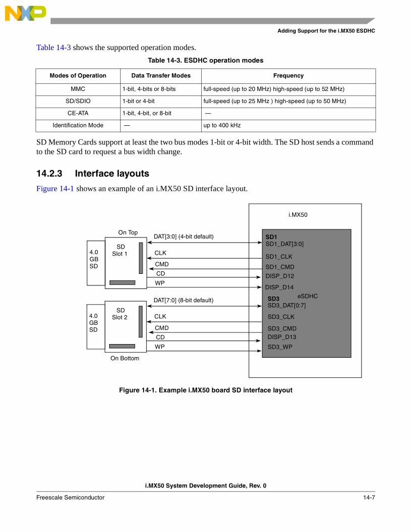
Adding Support for the i.MX50 ESDHC
i.MX50 System Development Guide, Rev. 0
Freescale Semiconductor 14-7
Table 14-3 shows the supported operation modes.
SD Memory Cards support at least the two bus modes 1-bit or 4-bit width. The SD host sends a command to the SD card to request a bus width change.
14.2.3 Interface layouts
Figure 14-1 shows an example of an i.MX50 SD interface layout.
Figure 14-1. Example i.MX50 board SD interface layout
Table 14-3. ESDHC operation modes
Modes of Operation Data Transfer Modes Frequency
MMC 1-bit, 4-bits or 8-bits full-speed (up to 20 MHz) high-speed (up to 52 MHz)
SD/SDIO 1-bit or 4-bit full-speed (up to 25 MHz ) high-speed (up to 50 MHz)
CE-ATA 1-bit, 4-bit, or 8-bit —
Identification Mode — up to 400 kHz
On Top
SDSlot 1
i.MX50
4.0 GBSD
SD1SD1_DAT[3:0]
SD1_CLK
SD1_CMD
DISP_D12
DAT[3:0] (4-bit default)
CLK
CMD
DISP_D14
CD
WP
SDSlot 24.0
GBSD
DAT[7:0] (8-bit default)
CLK
CMD
CD
WP
On Bottom
eSDHCSD3SD3_DAT[0:7]
SD3_CLK
SD3_CMDDISP_D13
SD3_WP
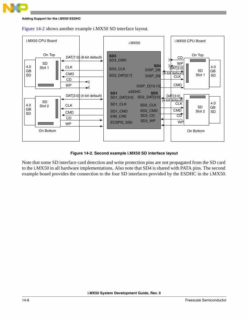
Adding Support for the i.MX50 ESDHC
i.MX50 System Development Guide, Rev. 0
14-8 Freescale Semiconductor
Figure 14-2 shows another example i.MX50 SD interface layout.
Figure 14-2. Second example i.MX50 SD interface layout
Note that some SD interface card detection and write protection pins are not propagated from the SD card to the i.MX50 in all hardware implementations. Also note that SD4 is shared with PATA pins. The second example board provides the connection to the four SD interfaces provided by the ESDHC in the i.MX50.
On Top
SDSlot 1
i.MX50
4.0 GBSD
SD3SD3_CMD
SD3_CLK
SD3_DAT[0:7]
DAT[7:0] (8-bit default)
CLK
CMD
CD
WP
SDSlot 24.0
GBSD
DAT[3:0] (4-bit default)
CLK
CMD
CD
WP
On Bottom
eSDHCSD1SD1_DAT[3:0]
SD1_CLK
SD1_CMDEIM_CRE
ECSPI2_SS0
i.MX50 CPU Board
On Top
SDSlot 1
4.0 GBSD
On Bottom
i.MX50 CPU Board
SDSlot 2
4.0 GBSD
SD4
SD2
CD
WPDAT[3:0]
(4-bit default)CLK
CMD
DISP_D8
DISP_D9
DISP_D[10:13]
DAT[3:0]
CD
WP
CMD
CLK(4-bit default)
SD2_DAT[3:0]
SD2_CLK
SD2_CMDSD2_CD
SD2_WP
i.MX50 System Development Guide, Rev. 0
Freescale Semiconductor 15-1
Chapter 15 Configuring the SPI NOR Flash Memory Technology Device (MTD) DriverThis chapter explains how to set up the SPI NOR Flash memory technology device (MTD) driver. This driver uses the SPI interface to support Atmel data Flash. By default, the SPI NOR Flash MTD driver creates static MTD partitions to support Atmel data Flash.
The NOR MTD implementation provides necessary information for the upper layer MTD driver.
15.1 Source code structureThe SPI NOR MTD driver is implemented in the following directory:<ltib_dir>/rpm/BUILD/linux/drivers/mtd/devices/mxc_dataflash.c
15.2 Configuration optionsBSP freescale supports the following ATMEL SPI NOR Flash models:
• "AT45DB011B" "at45db011d"
• "AT45DB021B" "at45db021d"
• "AT45DB041x" "at45db041d"
• "AT45DB081B" "at45db081d"
• "AT45DB161x" "at45db161d"
• "AT45DB321x" "at45db321d"
• "AT45DB642x" "at45db642d"
Those models are defined in the structure static struct flash_info __devinitdata dataflash_data[], located at <ltib_dir>/rpm/BUILD/linux/drivers/mtd/devices/mxc_dataflash.c.
The parameters are as follows:"at45db011d", 0x1f2200, 512, 256, 8, SUP_POW2PS | IS_POW2PS
Table 15-1 defines the variables.
Table 15-1. Parameter variables
Variable Definition
"at45db011d" Flash Name model
0x1F_2200 [5:4]Manufacter ID, [3:2]Device ID
512 Number of pages
Configuring the SPI NOR Flash Memory Technology Device (MTD) Driver
i.MX50 System Development Guide, Rev. 0
15-2 Freescale Semiconductor
NOTEIf you want to use another data flash model, add it on the last structure. Be sure the flash models are compatible with the Atmel data flashes.
15.3 Selecting SPI NOR on the Linux imageTable 15-2 provides information for each supported device.
Follow these steps to select the desired data flash from Table 15-2.
1. Open the mx50_<board name>.c file (located at arch/arm/mach-mx5/mx50_<board name>.c) and modify the structure called static struct flash_platform_data mxc_spi_flash_data[]
2. Write the name of the data flash desired on the .type variable of this structure. This name must be exactly the same as it appears on the dataflash_data[]_ structure.
3. Set the number of partitions you want to use on the SPI NOR Flash. On the mx50_<board name>.c file, go to the structure called static struct mtd_partition mxc_dataflash_partitions[]
Each partition has three elements: the name of the partition, the offset, and the size. By default, these elements are partitioned into a bootloader section and a kernel section, and defined as:
.name = "bootloader", .offset = 0, .size = 0x000100000, .name = "kernel", .offset = MTDPART_OFS_APPEND, .size = MTDPART_SIZ_FULL,
256 Number of bytes per page
8 Offset
Table 15-2. Device information
Device Density ID Code #Pages PageSize Offset
AT45DB011B 1 Mbit (128K) xx0011xx (0x0C) 512 264 9
AT45DB021B 2 Mbit (256K) xx0101xx (0x14) 1024 264 9
AT45DB041B 4 Mbit (512K) xx0111xx (0x1C) 2048 264 9
AT45DB081B 8 Mbit (1M) xx1001xx (0x24) 4096 264 9
AT45DB0161B 16 Mbit (2M) xx1011xx (0x2C) 4096 528 10
AT45DB0321B 32 Mbit (4M) xx1101xx (0x34) 8192 528 10
AT45DB0642 64 Mbit (8M) xx111xxx (0x3C) 8192 1056 11
AT45DB1282 128 Mbit (16M) xx0100xx (0x10) 16384 1056 11
Table 15-1. Parameter variables (continued)
Variable Definition

Configuring the SPI NOR Flash Memory Technology Device (MTD) Driver
i.MX50 System Development Guide, Rev. 0
Freescale Semiconductor 15-3
Bootloader starts from address 0 and has a size of 1 Mbyte. Kernel starts from address 1 Mbyte and has a size of 3 Mbytes.
NOTEYou may create more partitions or modify the size and names of these ones. To add more partitions, define another structure on the mxc_dataflash_partitions variable.
4. To get to the SPI NOR MTD driver, use the command ./ltib -c when located in the <ltib dir>.
5. On the screen displayed, select Configure the kernel and exit.
6. When the next screen appears, select the following option to enable the SPI NOR MTD driver:
CONFIG_MTD_MXC_DATAFLASH
This config enables access to the Atmel DataFlash chips, using FSL SPI. In menuconfig, this option is available under Device Drivers > Memory Technology Device (MTD) support > Self-contained MTD device drivers > Support for AT DataFlash via FSL SPI interface
15.4 Changing the SPI interface configurationThe i.MX50 chip has three CSPI interfaces: one CSPI and two ECSPI. By default, the i.MX50 BSP configures ECSPI-1 interface in the master mode to connect to the SPI NOR Flash. It also uses chip select 1 from this ECSPI interface (SS1).
The main difference between CSPI and ECSPI is the supported baud rate. CSPI supports up to 16 Mbps in master mode and ECSPI supports up to 66 Mbps.
15.4.1 Connecting SPI NOR Flash to another CSPI interface
Before connecting SPI NOR Flash to another CSPI, define the three things listed below:
• CSPI interface (between CSPI, ECSPI-1 or ECSPI-2).
• Chip select (between SS[3:0]).
• External signals
15.4.2 Changing the CSPI interface
To change the CSPI interface used, use the following procedure:
1. Locate the file at arch/arm/mach-mx5/mx50_<board name>.c
2. Look for the line mxc_register_device(&mxcspi1_device, &mxcspi1_data);
3. Use the function static void __init mxc_board_init(void) to register the CSPI-1 interface. To enable the other CSPI interface, replace the first parameter as shown in Table 15-3:
Table 15-3. CSPI parameters
CSPI Parameter name
ECSPI-1 &mxcspi1_device
Configuring the SPI NOR Flash Memory Technology Device (MTD) Driver
i.MX50 System Development Guide, Rev. 0
15-4 Freescale Semiconductor
15.4.3 Changing the chip select
To change the chip select used, locate the file at arch/arm/mach-mx5/mx50_<board name>.c and use the static struct spi_board_info mxc_dataflash_device[] __initdata structure.
Replace the value of ".chip_select" variable with the desired chip select value. For example, .chip_select = 3 sets the chip select to number 3 on the CSPI interface.
15.4.4 Changing the external signals
The iomux-mx50.h file contains the definitions for all i.MX50 pads. Add entries in this file to define the configuration for the CSPI function. See Chapter 13, “Configuring the IOMUX Controller (IOMUXC),” for a description of how to set up the IOMUX and pads for routing signals as desired.
NOTECheck the mxc_iomux_pins structure to ensure that the chosen signal chosen is not used by another interface before configuration.
15.5 Hardware operationSPI NOR Flash is SPI compatible with frequencies up to 66 MHz. The memory is organized in pages of 512 bytes or 528 bytes. SPI NOR Flash also contains two SRAM buffers of 512/528 bytes each, which allows data reception while a page in the main memory is being reprogrammed as well as the writing of a continuous data stream.
Unlike conventional Flash memories that are accessed randomly, the SPI NOR Flash accesses data sequentially. It operates from a single 2.7–3.6 V power supply for program and read operations.
SPI NOR Flashes are enabled through a chip select pin and accessed through a three-wire interface: serial input, serial output, and serial clock.
ECSPI-2 &mxcspi2_device
CSPI &mxcspi3_device
Table 15-3. CSPI parameters (continued)
CSPI Parameter name
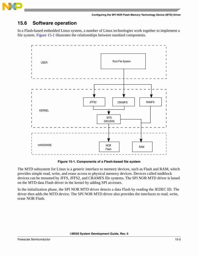
Configuring the SPI NOR Flash Memory Technology Device (MTD) Driver
i.MX50 System Development Guide, Rev. 0
Freescale Semiconductor 15-5
15.6 Software operationIn a Flash-based embedded Linux system, a number of Linux technologies work together to implement a file system. Figure 15-1 illustrates the relationships between standard components.
Figure 15-1. Components of a Flash-based file system
The MTD subsystem for Linux is a generic interface to memory devices, such as Flash and RAM, which provides simple read, write, and erase access to physical memory devices. Devices called mtdblock devices can be mounted by JFFS, JFFS2, and CRAMFS file systems. The SPI NOR MTD driver is based on the MTD data Flash driver in the kernel by adding SPI accesses.
In the initialization phase, the SPI NOR MTD driver detects a data Flash by reading the JEDEC ID. The driver then adds the MTD device. The SPI NOR MTD driver also provides the interfaces to read, write, erase NOR Flash.

Configuring the SPI NOR Flash Memory Technology Device (MTD) Driver
i.MX50 System Development Guide, Rev. 0
15-6 Freescale Semiconductor

i.MX50 System Development Guide, Rev. 0
Freescale Semiconductor 16-1
Chapter 16 Supporting the i.MX50 Reference Board LCDThis chapter explains how to support a new LCD on an i.MX50-based board. There are two options for adding support for a new LCD panel without modifying the BSP: letting the BSP calculate the timings using VESA defaults or reducing the blanking time. VESA and reduced blanking work for many LCDs but fail for some devices because of timing configuration constraints. For those devices, we need to modify the BSP and set the proper timing values. Modifying the boot arguments also allows us to include support for the new driver and load the driver by using the boot arguments.
This chapter focuses on the ELCDIF display interface. Common display cards can be attached to this interface. It provides connectivity for the Seiko 43WVF1G-0 WVGA LCD panel and the Chunghwa CLAA070VC01 WVGA LCD panel.
NOTEFSL i.MX50 reference design boards use some ELCDIF related pins for Ethernet pins, so if you would like to enable an LCD panel on these platforms, you need to disable Ethernet support in kernel menuconfig.
16.1 Supported display interfacesThe i.MX50 processor supports the E-INK display interfaces shown in Table 16-1.
16.2 Adding support for an LCD panelTo provide an example of how to add support for an LCD panel, this section shows the code and commands used for adding support for the CLAA070VC01 WVGA LCD panel. CLAA070VC01 is a 7" color TFT-LCD (thin film transistor liquid crystal display) module. It is composed of an LCD panel, driver ICs, control circuit, touch screen, and LED backlight. The 7" screen produces a high resolution image that is
Table 16-1. Available Interfaces
Feature ELCDIF (in i.MX50)
Number of ports Single display port
Legacy I/F • Parallel and serial • Synchronous (for display refresh) and asynchronous (to memory) Note: Serial display is not supported in the BSP because there is no available smart LCD
panel to be connected.
ITU-R BT.656 mode • Called digital video interface or DVI mode • includes progressive-to-interlace feature and RGB to YCbCr 4:2:2 color space
conversion to support 525/60Note: This mode is not supported in the BSP because the reference design boards do
not support the interface.
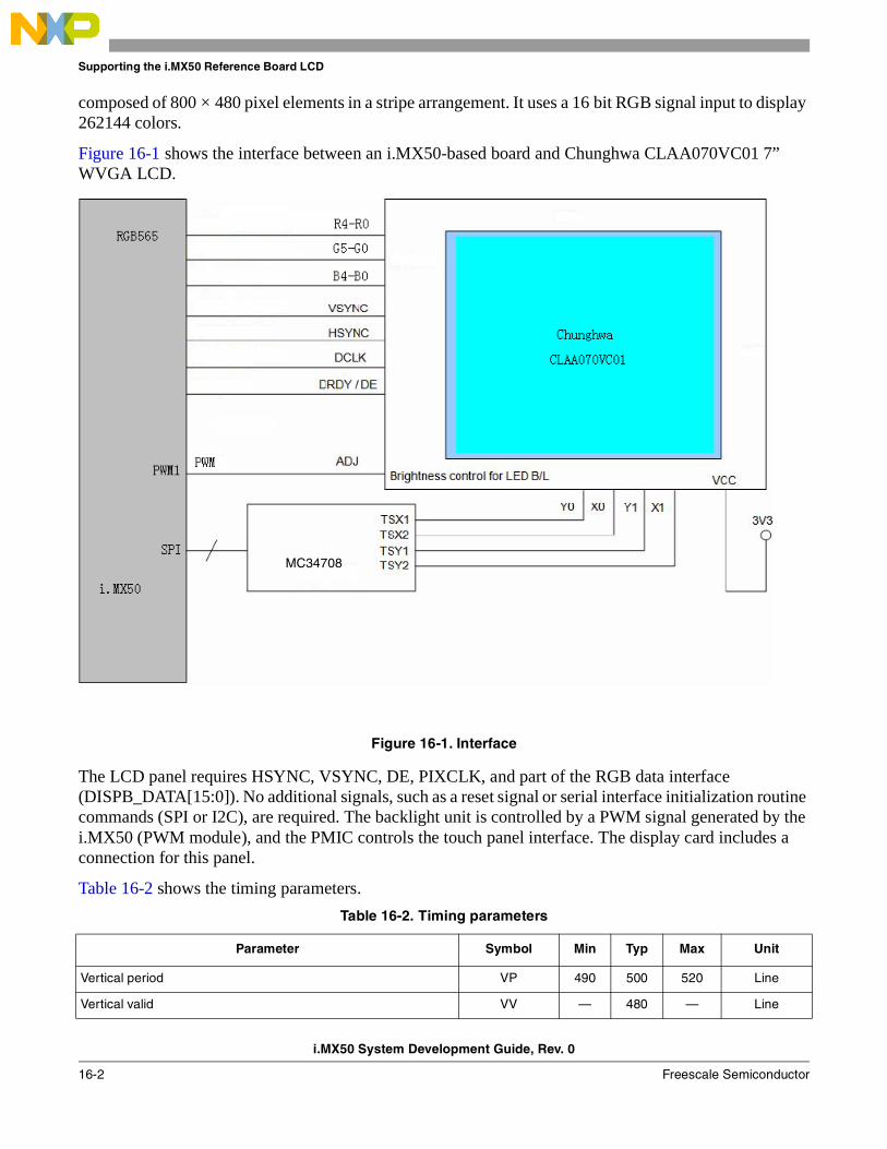
Supporting the i.MX50 Reference Board LCD
i.MX50 System Development Guide, Rev. 0
16-2 Freescale Semiconductor
composed of 800 × 480 pixel elements in a stripe arrangement. It uses a 16 bit RGB signal input to display 262144 colors.
Figure 16-1 shows the interface between an i.MX50-based board and Chunghwa CLAA070VC01 7” WVGA LCD.
Figure 16-1. Interface
The LCD panel requires HSYNC, VSYNC, DE, PIXCLK, and part of the RGB data interface (DISPB_DATA[15:0]). No additional signals, such as a reset signal or serial interface initialization routine commands (SPI or I2C), are required. The backlight unit is controlled by a PWM signal generated by the i.MX50 (PWM module), and the PMIC controls the touch panel interface. The display card includes a connection for this panel.
Table 16-2 shows the timing parameters.
Table 16-2. Timing parameters
Parameter Symbol Min Typ Max Unit
Vertical period VP 490 500 520 Line
Vertical valid VV — 480 — Line
MC34708
Supporting the i.MX50 Reference Board LCD
i.MX50 System Development Guide, Rev. 0
Freescale Semiconductor 16-3
16.3 Modifying boot kernel parameters to support a new LCDUsers can use the video mode parameter to change all timing and interface aspect ratios without writing a single line of code by changing the settings through the default driver.
16.3.1 Setting the video kernel parameter
The video kernel parameter is a multipurpose parameter used to configure display features. It controls the following features:
• Display resolution
• Pixel color depth
• Refresh rate
• ELCDIF output interface format
See the modedb.txt file located at Documentation/fb/modedb.txt for specific parameter information.
To set the parameter information for the video argument, use the following format. Variables between square brackets are optional.video=mxc_elcdif_fb:<xres>x<yres>[M][R][-<bpp>][@<refresh>][i][m]<name>[-<bpp>][@<refresh>]
Table 16-3 defines the variables.
Vertical blank VBK 10 20 40 Line
Vertical front porch VFP 1 11 46 Line
Vertical refresh rate FV 55 60 65 Hz
Horizontal period HP 850 900 950 PIXCLK
Horizontal valid HV — — — PIXCLK
Horizontal blank HBK 50 100 150 PIXCLK
Horizontal front porch HFP 64 114 214 PIXCLK
Dot clock FCLK 25 27 32.11 MHz
Table 16-3. Parameter information
Argument name Definition Units Values
name Video mode name NA String name
xres Horizontal resolution Pixels Decimal value
yres Vertical resolution Lines Decimal value
M Timing calculated using VESA(TM) NA M
R Timing using reduced blanking NA R
Table 16-2. Timing parameters (continued)
Parameter Symbol Min Typ Max Unit

Supporting the i.MX50 Reference Board LCD
i.MX50 System Development Guide, Rev. 0
16-4 Freescale Semiconductor
When <name> is included in the mode_option argument parameters, the timing is not calculated. Instead, it is extracted from BSP code. Valid default modes can be found at linux/drivers/video/modedb.c and in files placed at linux/drivers/video/mxc folder.
Example 16-1. CLAA070VC01 WVGA LCD
For a CLAA070VC01 WVGA LCD connected to ELCDIF display port, the kernel command is video=mxc_elcdif_fb:CLAA-WVGA (recommended)
video=mxc_elcdif_fb:800x480M@55,bpp=32
Table 16-4 shows how the values in this example correspond to the argument names defined in Table 16-3.
16.3.2 Modifying the bits per pixel setting
The default bits per pixel setting is 16 bits. To change the default value to another depth, modify the bpp parameter in video mode, for example bpp = 32. Please refer to Table 16-5.
Check the frame buffer bpp and other settings in the /sys/class folder. The output should look like the following: root@freescale ~$ cd /sys/class/graphics/fb0/root@freescale /sys/devices/platform/mxc_elcdif_fb/graphics/fb0$ cat bits_per_pixel32
Note that the final line shows the bits per pixel to be 32, reflecting our change from the default of 16 bpp.
bpp Bits per pixel on frame buffer Bits Decimal value (16 or 24)
refresh LCD refresh rate Hz Decimal value
Table 16-4. VGA LCD example variables
Argument Name Value Definition
name CLAA-WVGA Reflects the video mode defined in frame buffer platform data
xres 800 800 pixels (horizontal)
yres 480 480 lines (vertical)
M M Timing calculated using VESA (TM)
R Not used in this command —
bpp 32 Frame buffer is 32 bits per pixel
refresh 55 55 Hz
Table 16-3. Parameter information (continued)
Argument name Definition Units Values

Supporting the i.MX50 Reference Board LCD
i.MX50 System Development Guide, Rev. 0
Freescale Semiconductor 16-5
16.4 Adding support for a new LCDAdd the support for the new LCD in the BSP if neither VESA nor reducing the blanking calculation works for your LCD, or if you need a special function.
Perform the following steps to modify the i.MX50 BSP to add support for synchronous panels:
1. Add a display entry in the ltib catalog.
2. Create the madglobal LCD panel file.
3. Add compilation flag for the new display.
4. Configure LCD timings and display interface.
5. Use boot command to select the new LCD.
The following subsections describe these steps in detail.
16.4.1 Adding a display entry in the ltib catalog
To add an entry for a new LCD, perform the following steps:
1. Enter the i.MX50 display specific folder as follows.$ cd <ltib dir>/rpm/BUILD/linux/drivers/video/mxc
2. Open the Kconfig file with the command gedit Kconfig &
3. Use the following code to add the entry where you want it to appear. config FB_MXC_CLAA_SYNC_PANEL depends on FB_MXC_SYNC_PANEL tristate "CLAA WVGA Panel"
16.4.2 Creating the LCD panel file (initialization, reset, power settings, backlight)
Because power settings are handled by the ATLAS APL PMIC and other voltage regulators, the display driver must configure the APL PMIC during initialization to set up the power voltage configuration if this has not already been done. Also, the reset waveform and initialization routine must be included. To do these tasks, create an LCD file with panel-specific functions at the following location:<ltib dir>/rpm/BUILD/linux/drivers/video/mxc/mxcfb_CLAA_wvga.c
WARNINGBefore connecting an LCD panel to the i.MX50 board, check whether the LCD is powered with the proper supply voltages and whether the display data interface has the correct VIO value. Incorrect voltages and values may harm the device.
Supporting the i.MX50 Reference Board LCD
i.MX50 System Development Guide, Rev. 0
16-6 Freescale Semiconductor
The LCD file must include the definition of four basic functions described in Table 16-5 and can include other functions and macros as needed.
Next, create a platform device that can be loaded and unloaded. This example declares the new platform device using the devices.h and devices.c files located at:<ltib dir>//rpm/BUILD/linux/arch/arm/mach-mx5/
1. Add a new entry on madglobal:devices.c using the following:struct platform_device lcd_wvga_device = { { .name = "lcd_claa", .id = 0, },};
Be careful to use the same name for the new platform device entry as the name included in madglobal:mxcfb_claa_wvga.c for the driver. static struct platform_driver lcd_driver = { .driver = { .name = "lcd_claa"}, .probe = lcd_probe, .remove = __devexit_p(lcd_remove), .suspend = lcd_suspend, .resume = lcd_resume,};
2. Register the device at <ltib dir>//rpm/BUILD/linux/arch/arm/mach-mx5/madglobal:mx50_<reference board name>.c by using the following code: static int __init mxc_init_fb(void){ .... mxc_register_device(&lcd_wvga_device, NULL); .... return 0;}
Table 16-5. Required functions
Function name Function declaration Description
lcd_probe static int __devinit lcd_probe(struct platform_device *pdev)
Called when the LCD module is loaded. It should contain, pmic configuration, reset, power on sequence and the initialization routine.
lcd_remove static int __devexit lcd_remove(struct platform_device *pdev)
Called when the LCD module is removed. It should contain the power off PMIC configuration, the power off sequence, and the de-initialization routine.
lcd_suspend static int lcd_suspend(struct platform_device *pdev, pm_message_t state)
Not always implemented, but used to enhance low power modes on the device. Usually called when the system enters suspend mode.
lcd_resume static int lcd_resume(struct platform_device *pdev)
Not always implemented, but used to enhance low power modes on the device. Usually called when the system returns from suspend mode.
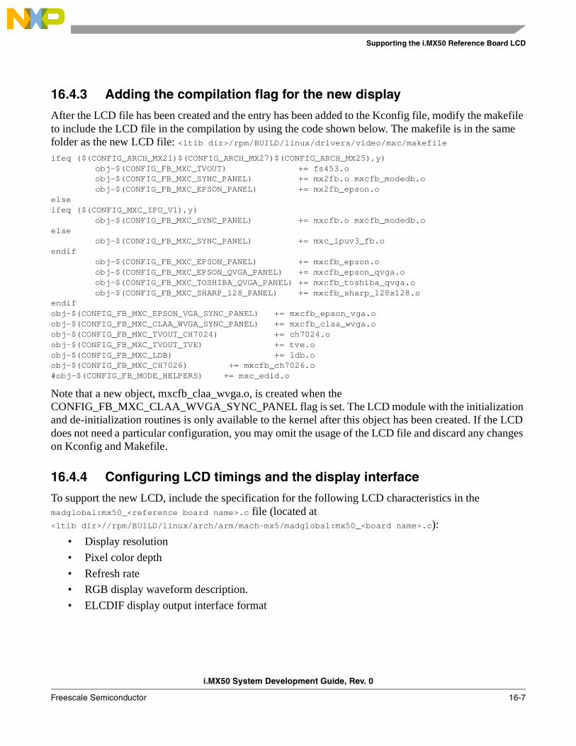
Supporting the i.MX50 Reference Board LCD
i.MX50 System Development Guide, Rev. 0
Freescale Semiconductor 16-7
16.4.3 Adding the compilation flag for the new display
After the LCD file has been created and the entry has been added to the Kconfig file, modify the makefile to include the LCD file in the compilation by using the code shown below. The makefile is in the same folder as the new LCD file: <ltib dir>/rpm/BUILD/linux/drivers/video/mxc/makefileifeq ($(CONFIG_ARCH_MX21)$(CONFIG_ARCH_MX27)$(CONFIG_ARCH_MX25),y)
obj-$(CONFIG_FB_MXC_TVOUT) += fs453.oobj-$(CONFIG_FB_MXC_SYNC_PANEL) += mx2fb.o mxcfb_modedb.oobj-$(CONFIG_FB_MXC_EPSON_PANEL) += mx2fb_epson.o
elseifeq ($(CONFIG_MXC_IPU_V1),y) obj-$(CONFIG_FB_MXC_SYNC_PANEL) += mxcfb.o mxcfb_modedb.oelse obj-$(CONFIG_FB_MXC_SYNC_PANEL) += mxc_ipuv3_fb.o endif
obj-$(CONFIG_FB_MXC_EPSON_PANEL) += mxcfb_epson.oobj-$(CONFIG_FB_MXC_EPSON_QVGA_PANEL) += mxcfb_epson_qvga.oobj-$(CONFIG_FB_MXC_TOSHIBA_QVGA_PANEL) += mxcfb_toshiba_qvga.oobj-$(CONFIG_FB_MXC_SHARP_128_PANEL) += mxcfb_sharp_128x128.o
endifobj-$(CONFIG_FB_MXC_EPSON_VGA_SYNC_PANEL) += mxcfb_epson_vga.oobj-$(CONFIG_FB_MXC_CLAA_WVGA_SYNC_PANEL) += mxcfb_claa_wvga.oobj-$(CONFIG_FB_MXC_TVOUT_CH7024) += ch7024.oobj-$(CONFIG_FB_MXC_TVOUT_TVE) += tve.oobj-$(CONFIG_FB_MXC_LDB) += ldb.oobj-$(CONFIG_FB_MXC_CH7026) += mxcfb_ch7026.o#obj-$(CONFIG_FB_MODE_HELPERS) += mxc_edid.o
Note that a new object, mxcfb_claa_wvga.o, is created when the CONFIG_FB_MXC_CLAA_WVGA_SYNC_PANEL flag is set. The LCD module with the initialization and de-initialization routines is only available to the kernel after this object has been created. If the LCD does not need a particular configuration, you may omit the usage of the LCD file and discard any changes on Kconfig and Makefile.
16.4.4 Configuring LCD timings and the display interface
To support the new LCD, include the specification for the following LCD characteristics in the madglobal:mx50_<reference board name>.c file (located at<ltib dir>//rpm/BUILD/linux/arch/arm/mach-mx5/madglobal:mx50_<board name>.c):
• Display resolution
• Pixel color depth
• Refresh rate
• RGB display waveform description.
• ELCDIF display output interface format
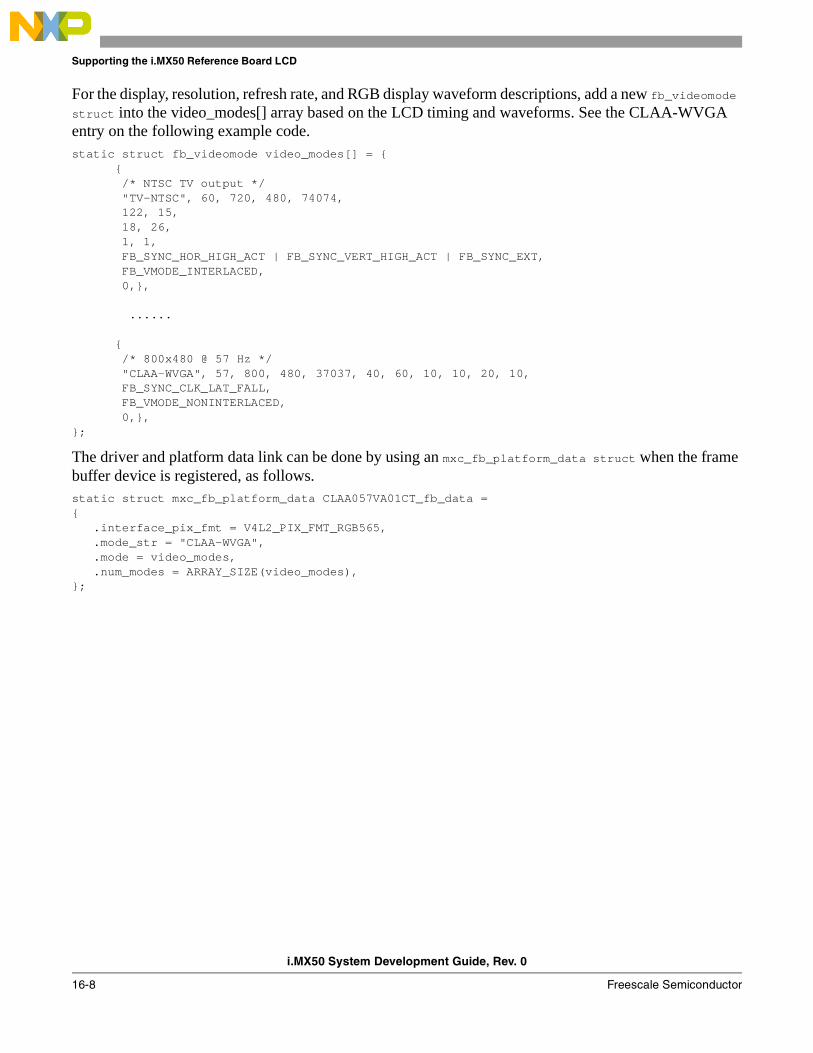
Supporting the i.MX50 Reference Board LCD
i.MX50 System Development Guide, Rev. 0
16-8 Freescale Semiconductor
For the display, resolution, refresh rate, and RGB display waveform descriptions, add a new fb_videomode struct into the video_modes[] array based on the LCD timing and waveforms. See the CLAA-WVGA entry on the following example code. static struct fb_videomode video_modes[] = { { /* NTSC TV output */ "TV-NTSC", 60, 720, 480, 74074, 122, 15, 18, 26, 1, 1, FB_SYNC_HOR_HIGH_ACT | FB_SYNC_VERT_HIGH_ACT | FB_SYNC_EXT, FB_VMODE_INTERLACED, 0,}, ...... { /* 800x480 @ 57 Hz */ "CLAA-WVGA", 57, 800, 480, 37037, 40, 60, 10, 10, 20, 10, FB_SYNC_CLK_LAT_FALL, FB_VMODE_NONINTERLACED, 0,},};
The driver and platform data link can be done by using an mxc_fb_platform_data struct when the frame buffer device is registered, as follows. static struct mxc_fb_platform_data CLAA057VA01CT_fb_data ={ .interface_pix_fmt = V4L2_PIX_FMT_RGB565, .mode_str = "CLAA-WVGA", .mode = video_modes, .num_modes = ARRAY_SIZE(video_modes),};
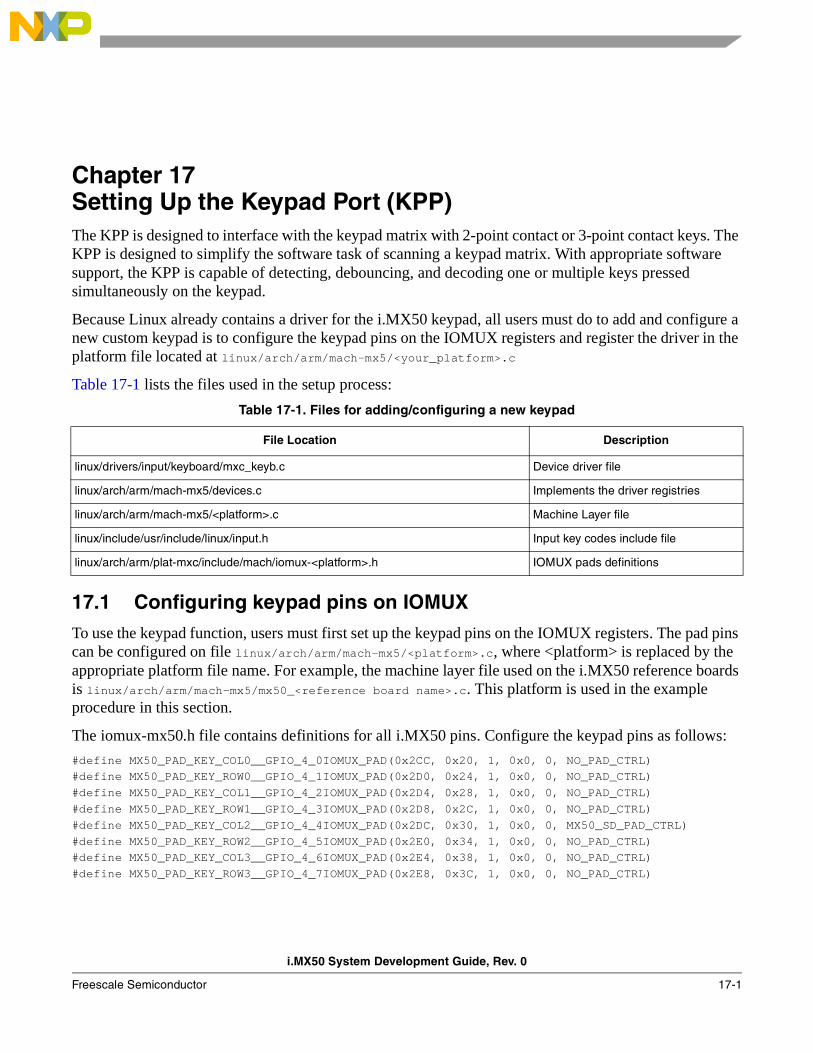
i.MX50 System Development Guide, Rev. 0
Freescale Semiconductor 17-1
Chapter 17 Setting Up the Keypad Port (KPP)The KPP is designed to interface with the keypad matrix with 2-point contact or 3-point contact keys. The KPP is designed to simplify the software task of scanning a keypad matrix. With appropriate software support, the KPP is capable of detecting, debouncing, and decoding one or multiple keys pressed simultaneously on the keypad.
Because Linux already contains a driver for the i.MX50 keypad, all users must do to add and configure a new custom keypad is to configure the keypad pins on the IOMUX registers and register the driver in the platform file located at linux/arch/arm/mach-mx5/<your_platform>.c
Table 17-1 lists the files used in the setup process:
17.1 Configuring keypad pins on IOMUXTo use the keypad function, users must first set up the keypad pins on the IOMUX registers. The pad pins can be configured on file linux/arch/arm/mach-mx5/<platform>.c, where <platform> is replaced by the appropriate platform file name. For example, the machine layer file used on the i.MX50 reference boards is linux/arch/arm/mach-mx5/mx50_<reference board name>.c. This platform is used in the example procedure in this section.
The iomux-mx50.h file contains definitions for all i.MX50 pins. Configure the keypad pins as follows:
#define MX50_PAD_KEY_COL0__GPIO_4_0IOMUX_PAD(0x2CC, 0x20, 1, 0x0, 0, NO_PAD_CTRL)#define MX50_PAD_KEY_ROW0__GPIO_4_1IOMUX_PAD(0x2D0, 0x24, 1, 0x0, 0, NO_PAD_CTRL)#define MX50_PAD_KEY_COL1__GPIO_4_2IOMUX_PAD(0x2D4, 0x28, 1, 0x0, 0, NO_PAD_CTRL)#define MX50_PAD_KEY_ROW1__GPIO_4_3IOMUX_PAD(0x2D8, 0x2C, 1, 0x0, 0, NO_PAD_CTRL)#define MX50_PAD_KEY_COL2__GPIO_4_4IOMUX_PAD(0x2DC, 0x30, 1, 0x0, 0, MX50_SD_PAD_CTRL)#define MX50_PAD_KEY_ROW2__GPIO_4_5IOMUX_PAD(0x2E0, 0x34, 1, 0x0, 0, NO_PAD_CTRL)#define MX50_PAD_KEY_COL3__GPIO_4_6IOMUX_PAD(0x2E4, 0x38, 1, 0x0, 0, NO_PAD_CTRL)#define MX50_PAD_KEY_ROW3__GPIO_4_7IOMUX_PAD(0x2E8, 0x3C, 1, 0x0, 0, NO_PAD_CTRL)
Table 17-1. Files for adding/configuring a new keypad
File Location Description
linux/drivers/input/keyboard/mxc_keyb.c Device driver file
linux/arch/arm/mach-mx5/devices.c Implements the driver registries
linux/arch/arm/mach-mx5/<platform>.c Machine Layer file
linux/include/usr/include/linux/input.h Input key codes include file
linux/arch/arm/plat-mxc/include/mach/iomux-<platform>.h IOMUX pads definitions
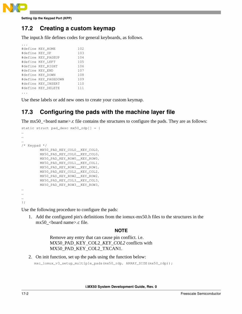
Setting Up the Keypad Port (KPP)
i.MX50 System Development Guide, Rev. 0
17-2 Freescale Semiconductor
17.2 Creating a custom keymapThe input.h file defines codes for general keyboards, as follows....#define KEY_HOME 102#define KEY_UP 103#define KEY_PAGEUP 104#define KEY_LEFT 105#define KEY_RIGHT 106#define KEY_END 107#define KEY_DOWN 108#define KEY_PAGEDOWN 109#define KEY_INSERT 110#define KEY_DELETE 111...
Use these labels or add new ones to create your custom keymap.
17.3 Configuring the pads with the machine layer fileThe mx50_<board name>.c file contains the structures to configure the pads. They are as follows:static struct pad_desc mx50_rdp[] = {………/* Keypad */
MX50_PAD_KEY_COL0__KEY_COL0,MX50_PAD_KEY_COL0__KEY_COL0,MX50_PAD_KEY_ROW0__KEY_ROW0,MX50_PAD_KEY_COL1__KEY_COL1,MX50_PAD_KEY_ROW1__KEY_ROW1,MX50_PAD_KEY_COL2__KEY_COL2,MX50_PAD_KEY_ROW2__KEY_ROW2,MX50_PAD_KEY_COL3__KEY_COL3,MX50_PAD_KEY_ROW3__KEY_ROW3,
………};
Use the following procedure to configure the pads:
1. Add the configured pin's definitions from the iomux-mx50.h files to the structures in the mx50_<board name>.c file.
NOTERemove any entry that can cause pin conflict. i.e. MX50_PAD_KEY_COL2_KEY_COL2 conflicts with MX50_PAD_KEY_COL2_TXCAN1.
2. On init function, set up the pads using the function below:mxc_iomux_v3_setup_multiple_pads(mx50_rdp, ARRAY_SIZE(mx50_rdp));

Setting Up the Keypad Port (KPP)
i.MX50 System Development Guide, Rev. 0
Freescale Semiconductor 17-3
3. Add the keymapping matrix as follows:static u16 keymapping[16] = {
KEY_UP, KEY_DOWN, KEY_MENU, KEY_BACK,KEY_RIGHT, KEY_LEFT, KEY_SELECT, KEY_ENTER,KEY_F1, KEY_F3, KEY_1, KEY_3,KEY_F2, KEY_F4, KEY_2, KEY_4,
};
4. Change the KEYS according to input.h labels and your keypad layout.
5. Add the following structure to configure the keypad:static struct keypad_data keypad_plat_data = {
.rowmax = 4,
.colmax = 4,
.learning = 0,
.delay = 2,
.matrix = keymapping,};
6. Register the keypad device. On the same machine layer file, add the following line on function mxc_board_init:
mxc_register_device(&mxc_keypad_device, &keypad_plat_data);
The new keypad is now implemented.
17.4 Enabling the keypadSelect the keypad on Linux menuconfig. This option is located at:
---> Device Drivers ---> Input device support ---> Keyboards ---> MXC Keypad Driver
Build the Linux kernel and boot the board.
17.5 Testing the keypadThere are two simple ways to test the keypad: using cat and using Evtest.
17.5.1 Using cat to test the keypad
On the i.MX50 Linux command line, type the following:cat /dev/input/keyboard0
ASCII characters are displayed when keys are pressed.
17.5.2 Using Evtest to test the keypad
Evtest is a simple software to test inputs. Build it by selecting the respective package on the ltib package list.
On the i.MX50 Linux command line, type the following:evtest /dev/input/keyboard0
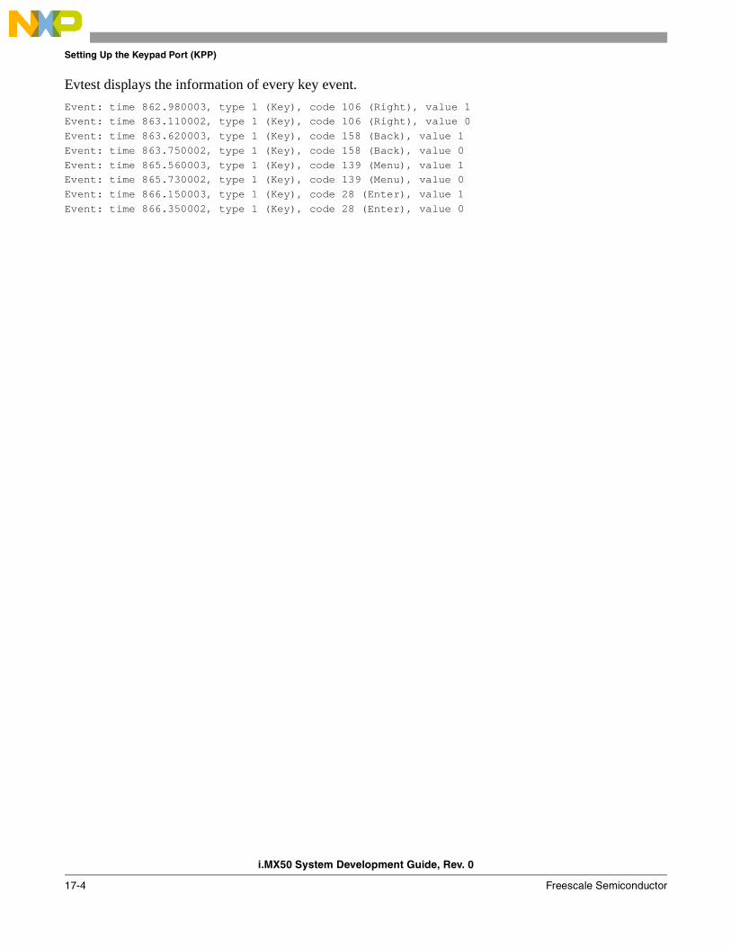
Setting Up the Keypad Port (KPP)
i.MX50 System Development Guide, Rev. 0
17-4 Freescale Semiconductor
Evtest displays the information of every key event.
Event: time 862.980003, type 1 (Key), code 106 (Right), value 1Event: time 863.110002, type 1 (Key), code 106 (Right), value 0Event: time 863.620003, type 1 (Key), code 158 (Back), value 1Event: time 863.750002, type 1 (Key), code 158 (Back), value 0Event: time 865.560003, type 1 (Key), code 139 (Menu), value 1Event: time 865.730002, type 1 (Key), code 139 (Menu), value 0Event: time 866.150003, type 1 (Key), code 28 (Enter), value 1Event: time 866.350002, type 1 (Key), code 28 (Enter), value 0
i.MX50 System Development Guide, Rev. 0
Freescale Semiconductor 18-1
Chapter 18 Porting Audio Drivers to a Custom BoardThis chapter explains how to port audio drivers from the Freescale reference BSP to a custom board. This procedure varies depending on whether the audio codec on the custom board is the same as or different than the audio codec on the Freescale reference design. This chapter first explains the common porting task and then the different porting tasks.
18.1 Common porting taskThe mxc_audio_platform_data structure must be defined and filled appropriately for the custom board before doing any other porting tasks. An example of a filled structure can be found in the file located at linux/arch/arm/mach-mx5/mx50_<board name>.c
static struct mxc_audio_platform_data sgtl5000_data = {.ssi_num = 1,.src_port = 2,.ext_port = 3,.hp_irq = IOMUX_TO_IRQ_V3(HP_DETECT),.hp_status = headphone_det_status,.amp_enable = mxc_sgtl5000_amp_enable,.clock_enable = mxc_sgtl5000_clock_enable,.sysclk = 12288000,
};
Customize the structure according to the following definitions:
ssi_num The ssi used for this codec
src_port The digital audio mux (DAM) port used for the internal SSI interface(for details about the internal functionality of the DAM please refer to the AUDMUX chapter of the i.MX50 Applications Processor Reference Manual)
ext_port The digital audio mux (DAM) port used for the external device audio interface (for details about the internal functionality of the DAM please refer to the AUDMUX chapter of the i.MX50 Applications Processor Reference Manual)
hp_irq The IRQ line used for headphone detection
hp_status A pointer to a function that returns the current headphone detect status. If a different mechanism or GPIO is used for headphone detect in the custom board, this function must be modified to accurately reflect the headphone presence.
amp_enable A pointer to a function that enables/disables the audio codec. For example, this function can be used to turn on or turn off the regulator supplying the audio codec.
init The initialization routine for the audio codec. Any setup necessary for the audio codec should be implemented in this function.
Porting Audio Drivers to a Custom Board
i.MX50 System Development Guide, Rev. 0
18-2 Freescale Semiconductor
18.2 Porting the reference BSP to a custom board (audio codec is the same as in the reference design)
When the audio codec is the same in the reference design and the custom board, users must ensure that the I/O signals and the power supplies to the codec are properly initialized in order to port the reference BSP to the custom board.
The iomux-mx50.h file contains the definitions for all pads. Add entries in this file to define the configuration for the audio codec signals. See Chapter 13, “Configuring the IOMUX Controller (IOMUXC),” for a description of how to set up the IOMUX and pads for routing signals as desired.
The necessary signals for the sgtl5000 codec, which is used on the reference board, are as follows:
• I2C interface signals
• I2S interface signals
• SSI external clock input to i.MX50
Table 18-1 shows the required power supplies for the sgtl5000 codec.
18.3 Porting the reference BSP to a custom board (audio codec is different than the reference design)
When adding support for an audio codec that is different than the one on the Freescale reference design, users must create new ALSA drivers in order to port the reference BSP to a custom board. The ALSA drivers plug into the ALSA sound framework, which allows the standard ALSA interface to be used to control the codec. Details about the ALSA infrastructure and developing ALSA drivers can be found at http://www.alsa-project.org/main/index.php/ASoC.
The source code for the ALSA driver is located in the Linux kernel source tree at linux/sound/soc. Table 18-2 shows the files used for the sgtl codec support:
Table 18-1. Required power supplies
Power Supply Name Definition Value
VDDD Digital voltage 1.98 V
VDDIO Digital IO voltage 3.6 V
VDDA Analog voltage 3.6 V
Table 18-2. Files for sgtl codec support
File Name Definition
imx-pcm.c • Shared by the stereo ALSA SoC driver, the 5.1 ALSA SoC driver, and the Bluetooth codec driver. • Responsible for preallocating DMA buffers and managing DMA channels.
imx-ssi.c • Registers the CPU DAI driver for the stereo ALSA SoC • Configures the on-chip SSI interfaces

Porting Audio Drivers to a Custom Board
i.MX50 System Development Guide, Rev. 0
Freescale Semiconductor 18-3
NOTEIf using a different codec, adapt the driver architecture shown in Table 18-2 accordingly. The exact adaptation will depend on the codec chosen. Obtain the codec-specific software from the codec vendor.
sgtl5000.c • Registers the stereo codec and Hi-Fi DAI drivers. • Responsible for all direct hardware operations on the stereo codec.
imx-3stack-sgtl5000.c • Machine layer code • Creates the driver device • Registers the stereo sound card.
Table 18-2. Files for sgtl codec support
File Name Definition

Porting Audio Drivers to a Custom Board
i.MX50 System Development Guide, Rev. 0
18-4 Freescale Semiconductor
i.MX50 System Development Guide, Rev. 0
Freescale Semiconductor 19-1
Chapter 19 Porting the Fast Ethernet Controller DriverThis chapter explains how to port the fast Ethernet controller (FEC) driver to the i.MX50 processor. Using Freescale’s standard (FEC) driver makes porting to the i.MX50 simple. Porting needs to address the following three areas:
• Pin configuration
• Source code
• Ethernet connection configuration
19.1 Pin configurationThe FEC supports three different standard physical media interfaces: a reduced media independent interface (RMII), a media independent interface (MII), and a 7-wire serial interface.
The Freescale hardware reference platform directly supports RMII, which has a reduced pin-count compared to MII. Therefore, RMII is the recommended interface.
Table 19-1 shows the signals used by the RMII interface.
Because the i.MX50 has more functionality than it has physical I/O pins, it uses I/O pin multiplexing. The general-purpose I/O pins (gpio1 GPIO[22–31]) default to ALT1.
The FEC_PHY_RESET_B signal comes up by default as gpio2 (pin #0), which is ALT function 1. This particular signal/pin is used as a simple GPIO to reset the FEC PHY. To use the pins as FEC signals mentioned above, configure them as the ALT0 function in the I/O multiplexer, except for FEC_PHY_RESET_B.
Table 19-1. RMII signals
Signal name Definition
FEC_TX_CLK (In, Synchronous clock reference)
FEC_TX_EN (Out, Transmit Enable)
FEC_TXD[0:1] (Out, Transmit Data)
FEC_RX_DV (In, Carrier Sense/Receive Data Valid)
FEC_RXD[0:1] (In, Receive Data)
FEC_RX_ER (In, Receive Error)
FEC_MDC (Out, Management Data Clock)
FEC_MDIO (In/Out, Management Data Input/Output)
FEC_PHY_RESET_B (In, PHY reset)

Porting the Fast Ethernet Controller Driver
i.MX50 System Development Guide, Rev. 0
19-2 Freescale Semiconductor
19.2 Source codeThe source code for the Freescale FEC Linux environment is located under the ../ltib/rpm/BUILD/linux/drivers/net directory. It contains the following files:
Of those files, only the FEC low-level Ethernet driver code (fec.[ch]) constitutes the Linux i.MX50 FEC driver.
The driver uses the following compile definitions:
CONFIG_FEC_1588 Set for IEEE 1588 network time synchronization.
CONFIG_M5272 PowerPC information. Can be safely ignored and should not be set.
CONFIG_MXC IMXxx parts. Should be defined.
CONFIG_MXS Legacy MXS part. Should generally not be defined.
19.3 Ethernet configurationThis section covers aspects such as duplex and speed configurations.
The two most common issues are as follows:
• MAC address is missing or invalid
• Ethernet connection (duplex, speed)
By default, the Ethernet driver reads the burned-in MAC address, which is found in code from the fec.c file located in the function fec_get_mac(). If no MAC address exists in the hardware, the MAC is read as all zeros, which creates problems. If this occurs, modify the code to read the MAC address from Flash or elsewhere.
The FEC driver and hardware are designed to comply to the IEEE standards for Ethernet auto-negotiation. See the FEC chapter in the i.MX50 Applications Processor Reference Manual for a description of using flow control in full duplex and more.
Table 19-2. Source code files
File Names
FEC low-level Ethernet driver: • fec.h • fec.c
MAC Switch software • fec_switch.h • fec_switch.c
IEEE 1588 PTP (network time sync) • fec_1588.h • fec_1588.c
MPC52xx PowerPC Ethernet Driver • fec_mpc52xx.h • fec_mpc52xx.c • fec_mpc52xx_phy.c
i.MX50 System Development Guide, Rev. 0
Freescale Semiconductor 20-1
Chapter 20 Porting USB Host1 and USB OTGThe USB Host1 and the USB OTG signals do not multiplex with other pins on the processor. Therefore, it is not necessary to port IOMUX settings for these interfaces when moving to a new platform.
The only required setup is as follows:
• For the USB Host1 PHY
— Supply USB_H1_VDDA33 with 3.3 V
— Supply USB_H1_VDDA25 with 2.5 V
• For the USB OTG PHY
— Supply USB_OTG_VDDA33 with 3.3 V
— Supply USB_OTG_VDDA25 with 2.5 V
The USB Host1 PHY uses the following signals:
• USB_H1_GPANAIO
• USB_H1_RREFEXT
• USB_H1_DP
• USB_H1_VDDA33
• USB_H1_DN
• USB_H1_VDDA25
• USB_H1_VBUS
The USB OTG PHY uses the following signals:
• USB_OTG_VBUS
• USB_OTG_ID
• USB_OTG_VDDA25
• USB_OTG_DN
• USB_OTG_VDDA33
• USB_OTG_DP
• USB_OTG_RREFEXT
• USB_OTG_GPANAIO