Embed Size (px)
Citation preview

Improving the RF Active Circuit Design Cycle Through
Innovations in Electrothermal Modeling, Characterization, and
Design Techniques Dr. Charles BaylisFaculty Candidate
April 11, 2008

School of Engineering & Computer Science
Overview• USF RACAM Research Group• The RF Active Circuit Design Cycle• Research Strategy/Overview• Nonlinear Modeling of Thermal and Trapping
Effects in GaN HEMTs• Radar Power Amplifier Combining Techniques
for Sidelobe Reduction• Prediction of Phase Noise in Amplifiers and
Frequency Multipliers• Development of Microwave Measurement
Techniques for Cell Cultures

School of Engineering & Computer Science
University of South Florida

School of Engineering & Computer Science
RACAM at USF
• 4 graduate students, 2 undergraduate students

School of Engineering & Computer Science
RF Active Circuit Design Cycle
Measurements Models
Design
Simulation
Fabrication
Testing
SUCCESS!!!Good models can eliminate this path.

School of Engineering & Computer Science
Strategy for Obtaining Funds
• Obtain initial grass-roots funding from industry contacts.
• From this foundation, apply for agency funding.

School of Engineering & Computer Science
Research Overview• Nonlinear Modeling for Power Amplifier Design
(Modelithics)$25,000 + $25,000 State Program Match = $50,000
• Prediction of Phase Noise in Amplifiers and Frequency Multipliers (Trak Microwave)$12,000 + $6,000 State Program Match = $18,000
• Investigation of Combining Techniques for Reduced Sidelobes in Radar Power AmplifiersNRL Proposal – March 2008, $170,000 for 2 years

School of Engineering & Computer Science
Research Overview
• Accurate Bio-Impedance Measurements NSF Proposal - February 2008, $361,381 for 3 years
• Research on a Wireless System for Transportation ApplicationsProposal to Sunovia Energy Systems, February 2008, 3
years
• Development of Model Scoring Metrics for RF Circuit DesignProposal to Raytheon RF Components (Andover,
Massachusetts), $49,500 for 1 year
School of Engineering & Computer Science
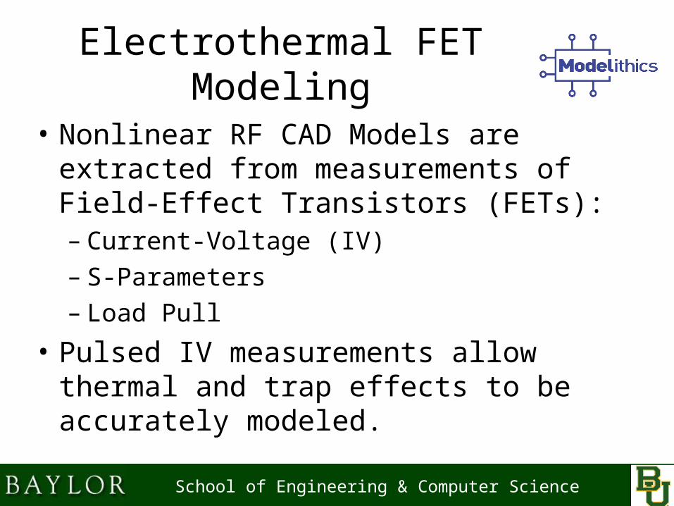
Electrothermal FET Modeling
• Nonlinear RF CAD Models are extracted from measurements of Field-Effect Transistors (FETs):– Current-Voltage (IV)– S-Parameters– Load Pull
• Pulsed IV measurements allow thermal and trap effects to be accurately modeled.

School of Engineering & Computer Science
IV Curves
• The IV curves give the boundaries for the large-signal performance of the FET:
ID
VDS
Drain-gate breakdownMaximum Current
Load line for signal swing
Knee Voltage

School of Engineering & Computer Science
Model Equation Fitting to IV
0.5 1.0 1.5 2.0 2.50.0 3.0
0.05
0.10
0.15
0.00
0.20
Vds (V)
Ids
(A)
Blue Dots = MeasuredRed Lines = Simulated
))exp(01)(tanh(tanh10 VTRVdgLSBVdsLAMBDAVdsIPKIds
))tanh(1( ALPHASALPHAR

School of Engineering & Computer Science
Pulsed IV Measurements• Static measurements
can be inaccurate for RF models.
• The cause: Slow Thermal and Trapping Processes
• Solutions: Pulsed IV and Measurements
• GaN HEMT Static (Dark Lines) and Pulsed IV (Light Lines)

School of Engineering & Computer Science
Pulsed IV Measurement • Measurements are performed during brief
(~0.2 μs) excursions from a quiescent bias. • The pulses are usually separated by at least 1
ms. • Thermal and trap conditions during the
measurement are those of the quiescent bias, as in high-frequency operation.

School of Engineering & Computer Science
Trapping Effects
• Trapping Effects in MESFETs
(Charbonninud et. al):– Substrate Traps– Surface Traps
• Electron Capture Fast Process• Electron Emission Slow Process
S G D
Electron Flow
Substrate Traps
Surface Traps

School of Engineering & Computer Science
Summary of Trap Processes
Q
Surface Hole Capture (Slow)
Surface Hole Emission (Fast)
Substrate Electron Emission (Slow)Surface Hole Capture (Slow)
Substrate Electron Capture (Fast)Surface Hole Emission (Fast)
FAST PROCESSES SLOW PROCESSES
ID
VDS

School of Engineering & Computer Science
Bias-Dependent Trapping
Gate: Drain

School of Engineering & Computer Science
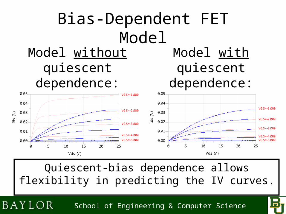
Bias-Dependent FET Model
Bias_Dependent_AngelovG6
Tccrf=0.0Tcrc=0.0Tclsb0=0.0Tccgd0=Tccgs0=
Tcp1=0.0006Tcipk0=-0.003Cth=Rth=60Crfin=Rcin=Crf=Rc=Rcmin=Tau=Lg=Ls=Ld=Rgd=Rs=0
Ri=0Rd=0Rg=0Vjg=Ne=Pg=Ij=P111=P41=P40=P31=P30=P21=P20=P11=
P10=Cgd0=Cgdpe=Cgdpi=Cgs0=Cgspi=Cds=Vsb2=Vtr=1Lsb0=0B2=0.09B1=0.0727224Lvg=0Lambda1=0Lambda=0.005599325921
Vkn=0.8Alphas=-1.0339968Alphar=1.215P3=0.03P2=0.121P1=0.456Dvpks=0.2Vpks=0Ipk0=0.0562LargeSignalHeat=0Vdsq=4Vgsq=-2Q3=0.018Q2=0.03Q1=0.39
New Parameters
School of Engineering & Computer Science
Bias-Dependent FET Model
Model without quiescent
dependence:
Model with quiescent
dependence:
5 10 15 200 25
0.01
0.02
0.03
0.04
0.00
0.05
VGS=-5.000
VGS=-4.000
VGS=-3.000
VGS=-2.000
VGS=-1.000
Vds (V)
Ids
(A)
5 10 15 200 25
0.01
0.02
0.03
0.04
0.00
0.05
VGS=-5.000VGS=-4.000
VGS=-3.000
VGS=-2.000
VGS=-1.000
Vds (V)Id
s (A
)
Quiescent-bias dependence allows flexibility in predicting the IV curves.

School of Engineering & Computer Science
Proposed Upcoming Work
• Adapt USF bias-dependent approach for use on other desired models.
• Add time-dependence of capture and emission trapping as well as thermal effects.
• Develop a straightforward characterization scheme for the bias and time dependence of thermal and trapping effects.

School of Engineering & Computer Science
Partial Jardel Circuit for Drain Traps*
Vds(t)
+
_
Vcont(t)
+
_
To calculations ofbackgating voltage
*O. Jardel, F. DeGroote, C. Charbonniaud, T. Reveyrand, J. Teyssier, R. Quere, and D. Floriot,“A Drain-Lag Model for AlGaN/GaN Power HEMTs,” IEEE International Microwave Symposium, Honolulu, Hawaii, June 2007.

School of Engineering & Computer Science
Radar Power Amplifiers – NRL Proposal
• Desire to reduce spectral sidelobes transmitted by shipboard radar systems.
• Chireix amplifier topology:

School of Engineering & Computer Science
Goals and Discussion
• Desired Isolation: 100 dB outside of 40 MHz bandwidth
• The pulsed signal and nonlinear amplifier use causes additional spectral components “spectral regrowth”.
Reprinted from J. de Graaf, H. Faust, J. Alatishe, and S. Talapatra, “Generation of Spectrally Confined Transmitted Radar Waveforms,” Proc. IEEE Conference on Radar, 2006, pp. 76-83
School of Engineering & Computer Science
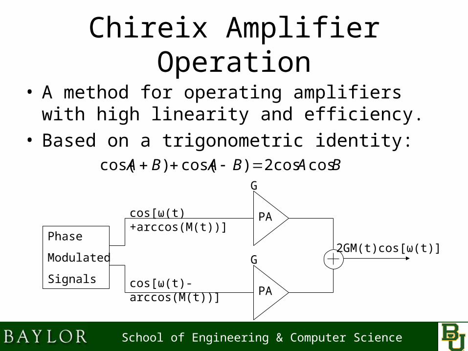
Chireix Amplifier Operation
• A method for operating amplifiers with high linearity and efficiency.
• Based on a trigonometric identity:BABABA coscos2)cos()cos(
Phase
Modulated
Signals
PA
PA
cos[ω(t)+arccos(M(t))]
cos[ω(t)-arccos(M(t))]
G
G2GM(t)cos[ω(t)]

School of Engineering & Computer Science 24
Combining Challenges
• A summer at microwave frequencies?• Combining Techniques
– 180-degree coupler– Chireix combiner
• A three-port network cannot be lossless, reciprocal, and matched at all ports.
• Pros and Cons– 180-degree coupler – matched, reciprocal, and lossy (3 dB)– Chireix combiner – unmatched, reciprocal, and lossless
School of Engineering & Computer Science 25
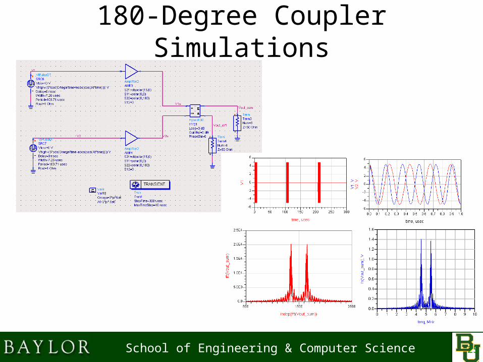
180-Degree Coupler Simulations

School of Engineering & Computer Science
Radar PA Combining – Upcoming Work
• Proposal to NRL for $170,000 over 2 years submitted March 2008
• Study different combining techniques:
• Examine rejection for better spectral masks.
• Continue simulation studies and eventually implement in hardware design improvements.
• Meeting with NRL at USF campus on April 14.

School of Engineering & Computer Science
Phase Noise Prediction• Tremendous consequences for system-level
design considerations.• Example: Phase Noise in 64-PSK Amplifier• Transistor 1/f noise is a source of phase noise.
• Project Goal: Predicting phase noise accurately in circuits through accurate modeling of 1/f noise.
ff
IKi
b
a
12
School of Engineering & Computer Science
Demonstration Circuits• Linear Amplifier
– Test phase noise prediction at multiple bias currents.– Si BJT, SiGe HBT.– Designed circuits presently in test phase.
• Frequency Multiplier– Test phase noise prediction due to self-biasing in
large-signal operation.– Si BJT, SiGe HBT.– Circuits presently in design phase.

School of Engineering & Computer Science
Microwaves and Bio – NSF Proposal
In collaboration with:

School of Engineering & Computer Science
Biological Motivation
• Tissue composition can often be investigated through permittivity measurements:
• Relative Permittivity Shows Three Dispersions:– Alpha Dispersion– Beta Dispersion– Gamma Dispersion
"'
Reprinted from H. Schwan, “Electrical Characteristicsof Tissues,” Biophysik, 1963, Vol. 1, No. 3, pp. 198-208

School of Engineering & Computer Science
Dispersions• Alpha Dispersion
– In kHz Range– Ionic diffusion (Foster and Schwan)– Measurable with Low Frequency Impedance Analyzer
• Beta Dispersion– Between 1 and 100 MHz– Capacitive charging of the cell membrane (Tamura et al.)– Can measure above this with microwave techniques
• Delta Dispersion– Varying causes– Between 0.1 and 3 GHz (Foster and Schwan)– Measurable by microwave techniques
• Gamma Dispersion– Dipole orientation in water molecules changes (Foster and
Schwan)– 20 to 25 GHz (depending on temperature)– Measurable by microwave techniques
School of Engineering & Computer Science
Measuring the Water Content of Cells
• Above the Beta Dispersion, the cell membrane (a capacitor) appears invisible to the electrical signal.
• The measured impedance above the Beta Dispersion is heavily dependent upon the water content of the cells.
• Cancer cells often have a higher water content than healthy cells (Foster and Schwan).
School of Engineering & Computer Science
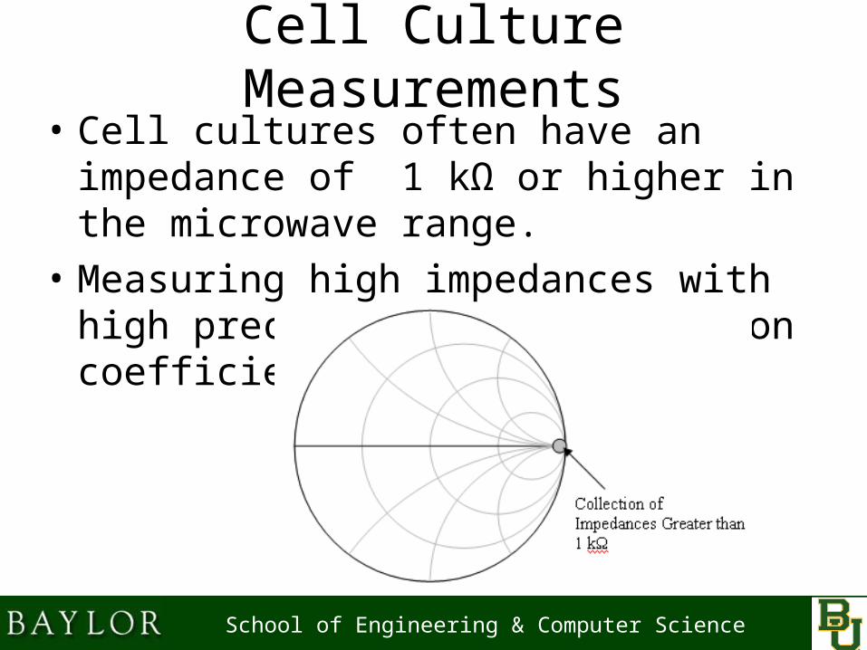
Cell Culture Measurements• Cell cultures often have an impedance of
1 kΩ or higher in the microwave range.
• Measuring high impedances with high precision using reflection coefficients is difficult:

School of Engineering & Computer Science
Microwave Measurement Technique for High Impedances
• New technique developed at Czech Technical University:
Reprinted from M. Randus and K. Hoffman, “A Simple Method for Extreme Impedances Measurement,” 70th Automatic RF Techniques Group (ARFTG)Conference, Tempe, Arizona, November 2007.

School of Engineering & Computer Science
Future Research
• Presently constructing system to verify method of Randus and Hoffman on large impedances.
• Modify cell culture impedance measurement setup of Prof. Shekhar Bhansali to perform microwave measurements.
• Examine applications (i.e. clinical detection of cancer)

School of Engineering & Computer Science
Conclusions
• An ambitious first-year approach has allowed expansion of USF’s modeling and characterization program into design and biological applications.
• A good industry base has been built, and agency proposals are being generated.
• A significant number of publications, as well as additional agency and industry proposals, are expected to be generated from the present work.

School of Engineering & Computer Science
Acknowledgments• Larry Cohen and Jean de Graaf, Naval
Research Laboratory• Christopher Reul, USF• Brent Seward, USF• Nathaniel Varney, USF• Dorielle Price, USF• Dr. Shekhar Bhansali, USF• Dr. Larry Dunleavy, USF and Modelithics, Inc.• Martin Randus, Czech Technical Institute• Dr. Karel Hoffman, Czech Technical Institute

School of Engineering & Computer Science
Thank you for your time and attention!