Embed Size (px)
Citation preview
MASTER THESIS
TITLE: Improving the efficiency of DC-DC converters by selecting an appropriate inductor current MASTER DEGREE: Master in Science in Telecommunication Engineering & Management AUTHOR: David López Salvadó DIRECTOR: Ferran Reverter Cubarsí DATE: December 19th 2014

Title: Improving the efficiency of DC-DC converters by selecting an appropriate inductor current Author: David López Salvadó Director: Ferran Reverter Cubarsí Date: December 19th 2014
Overview
The main goal of this project is to find an optimal current flowing through the DC-DC converter’s inductor during the energy transfer from the voltage source to the load. To do this, it has been proposed a circuit divided into two blocks: the first one is a DC-DC converter whose main function is to convert an input voltage into a higher output voltage and the second one is a comparator whose main function is to compare two different voltages to force the DC-DC converter working in PFM mode and more particular in burst mode. To find this optimal current, first of all we have to validate performing a circuit simulation with LTspice software and later design a PCB layout to test it. All tests consist in obtaining the behaviour of the DC-DC converter if certain critical values are modified such as the programmable resistance of the circuit to change the inductor’s current, the input voltage to simulate the wear that could may have the batteries, the output voltage of the circuit to emulate the circuits that require a different supply to operate and finally the output current of the circuit that emulates the current that can consume several circuits connected to the output of the DC-DC converter. As manufacturer says, in light-load conditions, this DC-DC converter has a very poor efficiency of 40% approximately working in PWM mode but if we change to PFM mode, this efficiency will double. To improve more the efficiency, burst mode is used and this efficiency will increase to 86% producing an enhancement of the efficiency between burst PFM mode and PWM of 49%.

ÍNDEX
INTRODUCTION ................................................................................................ 1
CHAPTER 1. DC-DC CONVERTERS ................................................................ 4
1.1. Introduction ............................................................................................................. 4 1.1.1. Types of DC-DC converters .................................................................... 5 1.1.1.1. Buck converters ......................................................................................... 5 1.1.1.2. Boost converter ......................................................................................... 6 1.1.1.3. Buck-Boost converter ................................................................................ 7 1.1.2. Operating modes ..................................................................................... 8 1.1.2.1. Pulse Width Modulation ............................................................................. 8 1.1.2.2. Pulse Frequency Modulation ..................................................................... 9 1.1.2.2.1. Burst mode .............................................................................................. 10 1.1.2.3. Advantages and drawbacks of PFM over PWM ...................................... 10
1.2. Boost converters .................................................................................................. 11 1.2.1. Operating principle................................................................................ 11 1.2.1.1. Continuous mode .................................................................................... 11 1.2.2. Topologies ............................................................................................. 14 1.2.2.1. Synchronous topology ............................................................................. 14
CHAPTER 2. PROPOSED OPERATING PRINCIPLE .................................... 15
2.1. Proposal circuit ..................................................................................................... 15 2.1.1. Batteries ................................................................................................. 15 2.1.2. Load ........................................................................................................ 15 2.1.3. DC-DC converter and comparator ....................................................... 16 2.1.3.1. DC-DC converter ..................................................................................... 16 2.1.3.2. Comparator .............................................................................................. 17
2.2. Power losses and efficiency ................................................................................ 17
CHAPTER 3. SIMULATIONS .......................................................................... 21
3.1. Simulation software .............................................................................................. 21 3.1.1. Hardware requirements ........................................................................ 21
3.2. Circuit design ........................................................................................................ 21 3.2.1. Comparator ............................................................................................ 22 3.2.1.1. Technical specifications .......................................................................... 23 3.2.1.2. Hysteresis ................................................................................................ 23 3.2.2. DC-DC converter .................................................................................... 24 3.2.2.1. Technical specifications .......................................................................... 25 3.2.2.2. Output voltage ......................................................................................... 26 3.2.2.3. Programmable resistor ............................................................................ 26
3.3. Operating principle ............................................................................................... 27 3.3.1. Effects of RP ........................................................................................... 29 3.3.2. Effects of VIN .......................................................................................... 31 3.3.3. Effects of IOUT ......................................................................................... 32
3.4. Efficiency ............................................................................................................... 33 3.4.1. Constrains about efficiency ................................................................. 35

CHAPTER 4. EXPERIMENTAL ANALYSIS .................................................... 36
4.1. Materials & method ............................................................................................... 36 4.1.1. Materials ................................................................................................. 37 4.1.2. Method .................................................................................................... 38 4.1.2.1. Input power .............................................................................................. 38 4.1.2.2. Output voltage ......................................................................................... 39 4.1.2.3. Output current .......................................................................................... 39 4.1.2.4. Output power ........................................................................................... 39
4.2. Efficiency ............................................................................................................... 39 4.2.1. Effects of IOUT ......................................................................................... 40 4.2.2. Effects of VOUT ........................................................................................ 42 4.2.3. Effects of VIN .......................................................................................... 44
CONCLUSIONS ............................................................................................... 48
REFERENCES ................................................................................................. 49
ABBREVIATONS ............................................................................................. 52
ANNEX 1. MATERIALS ................................................................................... 53
1.1. Boost DC-DC converter LTC3125 ........................................................................ 53
1.2. Comparator LTC1440............................................................................................ 54
1.3. Power supply Agilent E3631A ............................................................................. 55
1.4. Power analyser Yokogawa WT3000 .................................................................... 55
1.5. SMU Agilent B2901A............................................................................................. 56
1.6. Digital Multimeter Agilent 34410A ....................................................................... 56
1.7. LTSpice IV simulation software ........................................................................... 57
1.7.1. Transient command .............................................................................................. 57
1.7.2. Initial conditions ................................................................................................... 58
ANNEX 2. EFFICIENCY .................................................................................. 59
2.1. Efficiency simulation ............................................................................................ 59

INTRODUCTION 1
INTRODUCTION Nowadays, power management is becoming increasingly important in the electrical engineering industry due to the advances in the electronics and technology that are taking place. With these advances, comes a reduction in the available space for the circuit produced, therefore, the necessity to reduce the size of the components that manages power to the circuit (batteries). This reduction size usually involves that batteries have less power to deliver so, arises the need for increasing the lifetime of the batteries. These batteries are used to power many types of sensors and low-power autonomous systems among others. The output of these batteries is processed by a DC-DC converter. There are three types of DC-DC converters (buck, boost and buck-boost) that are explained in more detail in the first chapter. We decide to use a boost DC-DC converter because we want to convert the voltage provided by the two batteries (3V) into a higher voltage that is typically consumed by the circuits connected to the output (5V). The commercial DC-DC converter used is LTC3125 because, as manufacturer says, this converter is able to work in two operating modes (PFM and PWM) and can work in between our input and output voltage range. The loads we want to power are sensors node, low-power autonomous systems, tablets or laptops in sleep mode among others. These loads consume low current (≤ X0mA) and because of this, these loads are called light-loads. In Fig. 1 how the efficiency for light-loads is less than 50% Fig. 1 shows how the efficiency depends on load current and input voltage for a fixed value of output voltage
Fig. 1 Efficiency versus load current for different values of VIN and VOUT = 5V [1]
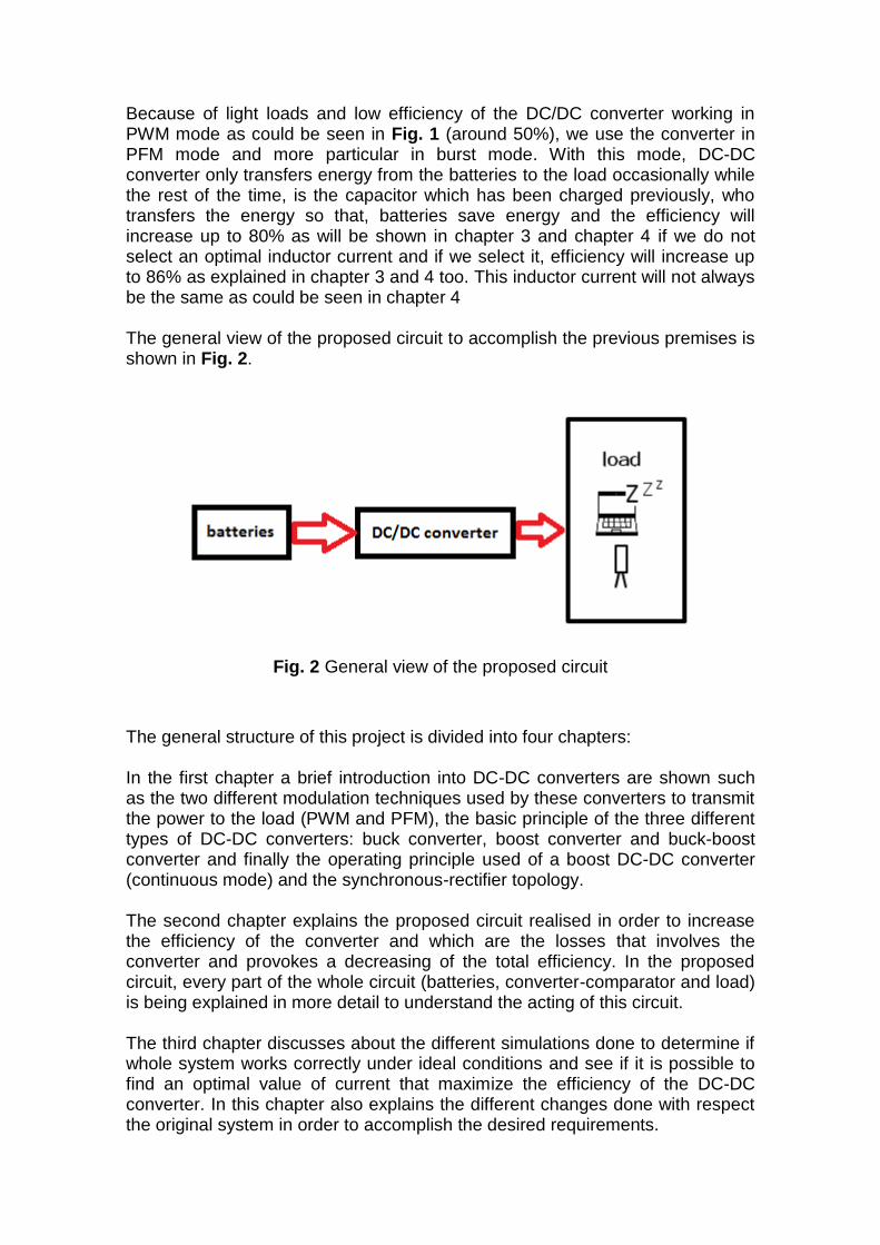
Because of light loads and low efficiency of the DC/DC converter working in PWM mode as could be seen in Fig. 1 (around 50%), we use the converter in PFM mode and more particular in burst mode. With this mode, DC-DC converter only transfers energy from the batteries to the load occasionally while the rest of the time, is the capacitor which has been charged previously, who transfers the energy so that, batteries save energy and the efficiency will increase up to 80% as will be shown in chapter 3 and chapter 4 if we do not select an optimal inductor current and if we select it, efficiency will increase up to 86% as explained in chapter 3 and 4 too. This inductor current will not always be the same as could be seen in chapter 4 The general view of the proposed circuit to accomplish the previous premises is shown in Fig. 2.
Fig. 2 General view of the proposed circuit
The general structure of this project is divided into four chapters: In the first chapter a brief introduction into DC-DC converters are shown such as the two different modulation techniques used by these converters to transmit the power to the load (PWM and PFM), the basic principle of the three different types of DC-DC converters: buck converter, boost converter and buck-boost converter and finally the operating principle used of a boost DC-DC converter (continuous mode) and the synchronous-rectifier topology. The second chapter explains the proposed circuit realised in order to increase the efficiency of the converter and which are the losses that involves the converter and provokes a decreasing of the total efficiency. In the proposed circuit, every part of the whole circuit (batteries, converter-comparator and load) is being explained in more detail to understand the acting of this circuit. The third chapter discusses about the different simulations done to determine if whole system works correctly under ideal conditions and see if it is possible to find an optimal value of current that maximize the efficiency of the DC-DC converter. In this chapter also explains the different changes done with respect the original system in order to accomplish the desired requirements.

INTRODUCTION 3
The fourth chapter discusses about the experimental tests done with the system and a comparison of these results with respect those obtained on the simulation chapter. This chapter will also show the optimal inductor current for each case depending on the effects of changing the critical values of the output current, the output voltage and the input voltage. Finally, conclusions extracted from the tests performed are explained.

4 IMPROVING THE EFFICIENCY OF DC-DC CONVERTERS BY SELECTING AN APPROPIATE INDUCTOR CURRENT
CHAPTER 1. DC-DC CONVERTERS
1.1. Introduction
Power supply is an electronic device that supplies electric energy to a load and allows us to design electronic circuits and systems. All electronic circuits require power supply but not all can operate well with AC supply; many electronic systems require only DC supply voltage. This DC supply voltage is usually supplied from a battery or an AC line using transformers, rectifiers or filters. The DC voltage achieved is not enough constant and high AC ripple is not appropriate for most applications and, because of this, voltage regulators are used. There are some categories of voltage regulators but in this master thesis, SMPS are studied and in more particularly boost DC-DC converters. A DC-DC converter is an electronic circuit that transfers energy from a DC voltage source to a load. First of all, the energy is transferred via electronic switches, such as transistors or diodes, to the energy storage devices, such as inductors or capacitors, and subsequently switched from these storage devices to the load. This process of energy transfer results in an output voltage that could be lower or higher than the input and is related to the input voltages by the duty ratio of the switches. These devices can work in two operating modes:
Continuous mode: in this mode, the current through the inductor (IL) never reach to zero.
Discontinuous mode: in this mode, the current through the inductor (IL) fails to zero during part of the period
Both operating modes will explain in more details The main advantages that these devices will provide are the high efficiency, the small components used and finally, the energy stored by an inductor in the switching regulator can be transformed to output voltages that can be greater than the input (boost converter), lower than the input (buck converter), greater or lower alternatively (buck-boost converter), negative voltage (inverter converter) or can even be transferred through a transformer to provide electrical isolation with respect to the input. On the other hand, the drawbacks of these devices are that are noisy devices and requires an energy management on the control loop. Fig. 1.1 shows the block diagram of a DC-DC converter which contains two main blocks: the power processor and the feedback controller. The feedback part is the responsible of adjusting the power transfer by generating corrective signals to keep the output voltage between the desired voltages.
DC-DC CONVERTERS 5
Fig. 1.1 Block diagram of a DC-DC converter
Depending on the output voltage (VOUT), these devices are called step-up converters (boost), step-down converters (buck), buck-boost converters or inverting converters as explained below.
1.1.1. Types of DC-DC converters
Depending on the isolation of the converter between the input and the output, there are two different types of DC-DC converters:
Non-isolated: there are four basic types: o Buck converter: converts a high voltage into a lower one. These devices
are also called step-down converters.
o Boost converter: converts a low voltage into a higher one. These devices are also called step-up converters.
o Buck-boost converter: produces a fixed output voltage when the input voltage is either higher or lower than the output voltage.
o Inverting converter: produces a negative voltage from a positive one.
Isolated: there is isolation between the input and the output. The main advantages of these devices is that the output can be configured to be positive or negative offering a barrier with a high frequency transformer in order to make it safety because need a separation between the input and the output that is user accessible. We are not focused in this type of converters.
1.1.1.1. Buck converters
A buck converter is a DC-DC converter whose output voltage can be less or equal than the input one. It is a class of SMPS that contains, at least, two semiconductors (diodes or transistors) and one energy storage element (inductor or capacitor) and they are also called step-down converters.

6 IMPROVING THE EFFICIENCY OF DC-DC CONVERTERS BY SELECTING AN APPROPIATE INDUCTOR CURRENT
The basic operating principle of a buck converter consists in two different stages depending on the state of the switch:
The power stage of the ON state of the switch when it is closed and diode D is reverse-biased is shown in Fig 1.2. In this stage the current through the inductor L rises linearly and the inductor is storing energy.
Fig. 1.2 ON state of the switch
The power stage of the OFF state of the switch when it is opened and the diode D is forward biased is shown in Fig 1.3. In this stage, current through the inductor decreases because the inductor is discharging its stored energy into the load.
Fig. 1.3 OFF state of the switch
1.1.1.2. Boost converter
A boost converter is a DC-DC converter with an output voltage greater than the input. It is a class of SMPS that contains, at least, two semiconductors (diodes or transistors) and one energy storage element (inductor or capacitor). These types of converters are also called step-up converters. The basic operating principle of a boost converter consists in two different stages depending on the state of the switch:
The power stage of the ON state of the switch when it is closed is shown in Fig 1.4. In this stage the current through the inductor increases and flows in clockwise direction storing energy. The blocking diode D prevents the capacitor C from discharging to the switch and this capacitor is able to deliver stored energy during the OFF state to the load.
DC-DC CONVERTERS 7
Fig. 1.4 ON state of the switch
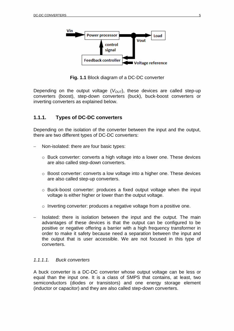
The power stage of the OFF state of the switch when it is opened is shown in Fig 1.5. The only path offered to flow the inductor current is through the diode D, the capacitor C and the load R.
Fig. 1.5 OFF state of the switch
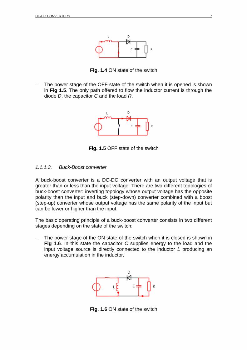
1.1.1.3. Buck-Boost converter
A buck-boost converter is a DC-DC converter with an output voltage that is greater than or less than the input voltage. There are two different topologies of buck-boost converter: inverting topology whose output voltage has the opposite polarity than the input and buck (step-down) converter combined with a boost (step-up) converter whose output voltage has the same polarity of the input but can be lower or higher than the input. The basic operating principle of a buck-boost converter consists in two different stages depending on the state of the switch:
The power stage of the ON state of the switch when it is closed is shown in Fig 1.6. In this state the capacitor C supplies energy to the load and the input voltage source is directly connected to the inductor L producing an energy accumulation in the inductor.
Fig. 1.6 ON state of the switch
8 IMPROVING THE EFFICIENCY OF DC-DC CONVERTERS BY SELECTING AN APPROPIATE INDUCTOR CURRENT
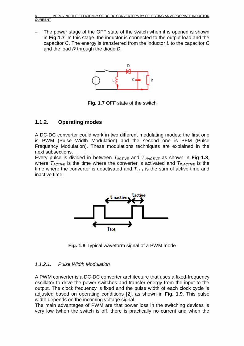
The power stage of the OFF state of the switch when it is opened is shown in Fig 1.7. In this stage, the inductor is connected to the output load and the capacitor C. The energy is transferred from the inductor L to the capacitor C and the load R through the diode D.
Fig. 1.7 OFF state of the switch
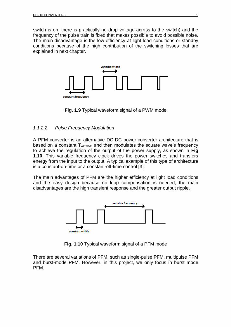
1.1.2. Operating modes
A DC-DC converter could work in two different modulating modes: the first one is PWM (Pulse Width Modulation) and the second one is PFM (Pulse Frequency Modulation). These modulations techniques are explained in the next subsections. Every pulse is divided in between TACTIVE and TINACTIVE as shown in Fig 1.8, where TACTIVE is the time where the converter is activated and TINACTIVE is the time where the converter is deactivated and TTOT is the sum of active time and inactive time.
Fig. 1.8 Typical waveform signal of a PWM mode
1.1.2.1. Pulse Width Modulation
A PWM converter is a DC-DC converter architecture that uses a fixed-frequency oscillator to drive the power switches and transfer energy from the input to the output. The clock frequency is fixed and the pulse width of each clock cycle is adjusted based on operating conditions [2], as shown in Fig. 1.9. This pulse width depends on the incoming voltage signal. The main advantages of PWM are that power loss in the switching devices is very low (when the switch is off, there is practically no current and when the
DC-DC CONVERTERS 9
switch is on, there is practically no drop voltage across to the switch) and the frequency of the pulse train is fixed that makes possible to avoid possible noise. The main disadvantage is the low efficiency at light load conditions or standby conditions because of the high contribution of the switching losses that are explained in next chapter.
Fig. 1.9 Typical waveform signal of a PWM mode
1.1.2.2. Pulse Frequency Modulation
A PFM converter is an alternative DC-DC power-converter architecture that is based on a constant TACTIVE and then modulates the square wave’s frequency to achieve the regulation of the output of the power supply, as shown in Fig 1.10. This variable frequency clock drives the power switches and transfers energy from the input to the output. A typical example of this type of architecture is a constant-on-time or a constant-off-time control [3]. The main advantages of PFM are the higher efficiency at light load conditions and the easy design because no loop compensation is needed; the main disadvantages are the high transient response and the greater output ripple.
Fig. 1.10 Typical waveform signal of a PFM mode
There are several variations of PFM, such as single-pulse PFM, multipulse PFM and burst-mode PFM. However, in this project, we only focus in burst mode PFM.
10 IMPROVING THE EFFICIENCY OF DC-DC CONVERTERS BY SELECTING AN APPROPIATE INDUCTOR CURRENT
1.1.2.2.1. Burst mode
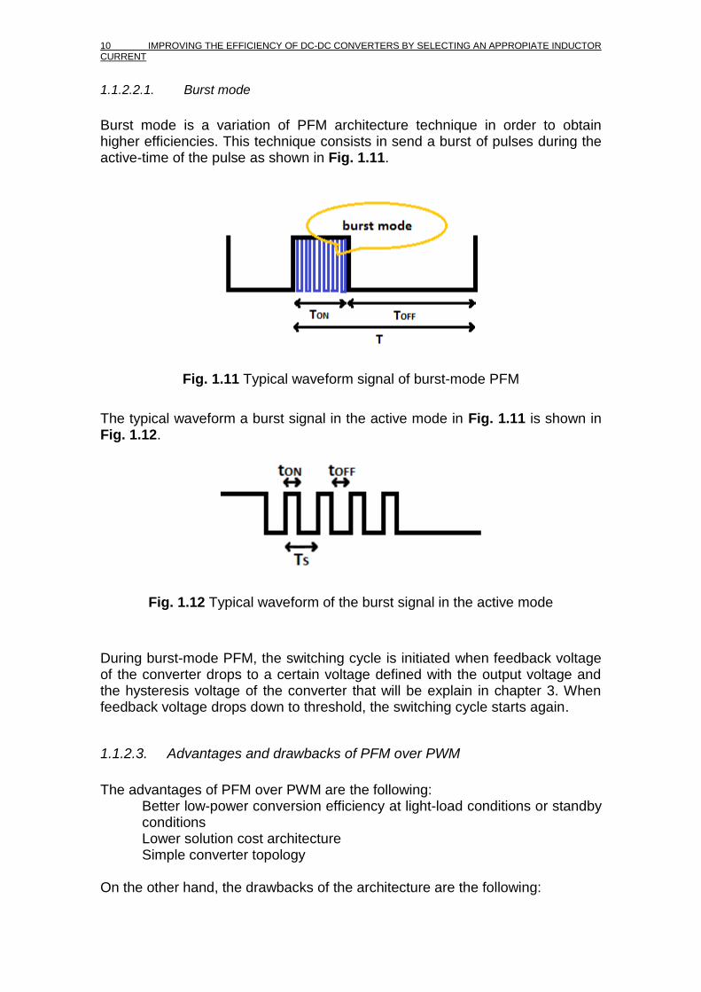
Burst mode is a variation of PFM architecture technique in order to obtain higher efficiencies. This technique consists in send a burst of pulses during the active-time of the pulse as shown in Fig. 1.11.
Fig. 1.11 Typical waveform signal of burst-mode PFM
The typical waveform a burst signal in the active mode in Fig. 1.11 is shown in Fig. 1.12.
Fig. 1.12 Typical waveform of the burst signal in the active mode
During burst-mode PFM, the switching cycle is initiated when feedback voltage of the converter drops to a certain voltage defined with the output voltage and the hysteresis voltage of the converter that will be explain in chapter 3. When feedback voltage drops down to threshold, the switching cycle starts again.
1.1.2.3. Advantages and drawbacks of PFM over PWM
The advantages of PFM over PWM are the following:
Better low-power conversion efficiency at light-load conditions or standby conditions Lower solution cost architecture Simple converter topology
On the other hand, the drawbacks of the architecture are the following:
DC-DC CONVERTERS 11
Greater output voltage ripple that can cause problems to the load Increasing of the transient response at lower frequencies → can cause slow response and a consumer disappointment in portable applications
1.2. Boost converters
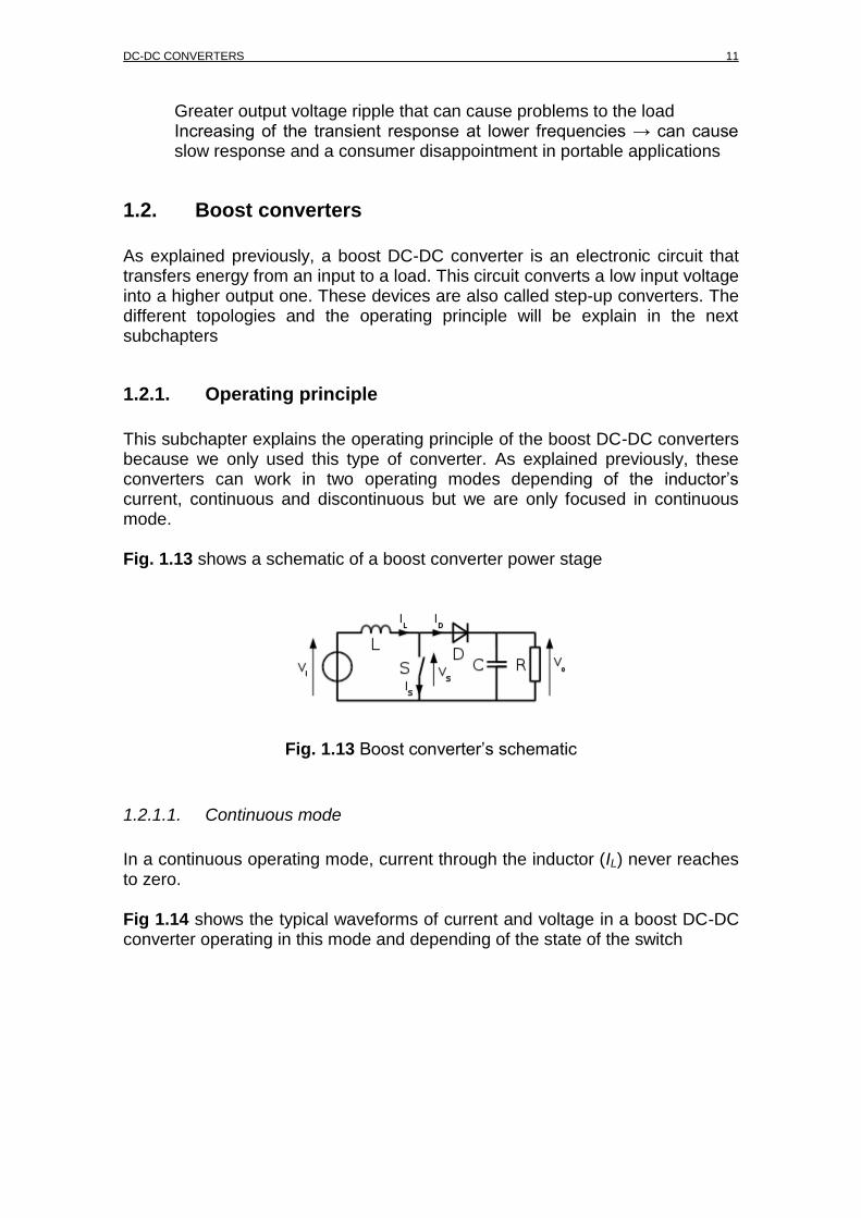
As explained previously, a boost DC-DC converter is an electronic circuit that transfers energy from an input to a load. This circuit converts a low input voltage into a higher output one. These devices are also called step-up converters. The different topologies and the operating principle will be explain in the next subchapters
1.2.1. Operating principle
This subchapter explains the operating principle of the boost DC-DC converters because we only used this type of converter. As explained previously, these converters can work in two operating modes depending of the inductor’s current, continuous and discontinuous but we are only focused in continuous mode. Fig. 1.13 shows a schematic of a boost converter power stage
Fig. 1.13 Boost converter’s schematic
1.2.1.1. Continuous mode
In a continuous operating mode, current through the inductor (IL) never reaches to zero. Fig 1.14 shows the typical waveforms of current and voltage in a boost DC-DC converter operating in this mode and depending of the state of the switch

12 IMPROVING THE EFFICIENCY OF DC-DC CONVERTERS BY SELECTING AN APPROPIATE INDUCTOR CURRENT
Fig. 1.14 Waveforms of current and voltage in continuous mode
During the ON state, the switch S is closed which makes the input voltage (VIN) appears across the inductor L. Diode D prevents capacitor C from discharging to ground. The voltage across the inductor causes a change in the inductor current (ΔIL) flowing through the inductor during a time period Δt following the eq. 1.1.
Δ𝐼𝐿
Δ𝑡=
𝑉𝐼𝑁
𝐿 (1.1)
At the end of this state, the increase of inductor’s current (ΔILon) is:
Δ𝐼𝐿𝑜𝑛 =1
𝐿∫ 𝑉𝐼𝑁 ∙ 𝑑𝑡 =
𝐷𝑇
𝐿∙ 𝑉𝐼𝑁
𝐷𝑇
0 (1.2)
where D is the duty cycle and its value is in between 0 (switch S is always off) and 1 (switch S is always on). During the OFF state, the switch S is open and the inductor current flows through the load. Zero voltage dropped in the diode and a capacitor large enough for its voltage to remain constant is considered in order to obtain the evolution of IL:
𝑉𝐼𝑁 − 𝑉𝑂𝑈𝑇 = 𝐿 ∙𝑑𝐼𝐿
𝑑𝑡 (1.3)
Therefore, the variation of IL during this state is:
DC-DC CONVERTERS 13
Δ𝐼𝐿𝑜𝑓𝑓 = ∫(𝑉𝐼𝑁−𝑉𝑂𝑈𝑇)∙𝑑𝑡
𝐿=
(𝑉𝐼𝑁−𝑉𝑂𝑈𝑇)∙(1−𝐷)∙𝑇
𝐿
𝑇
𝐷𝑇 (1.4)
Because of the converter has been considered working in steady-state conditions, the amount of energy stored in each of its components has to be the same at the beginning and at the end of a commutation cycle. In particular, the energy stored in the inductor is given by:
𝐸 =1
2∙ 𝐿 ∙ 𝐼𝐿
2 (1.5)
The above premise means that the overall current’s change has to be zero: Δ𝐼𝐿𝑜𝑛 + Δ𝐼𝐿𝑜𝑓𝑓 = 0 (1.6)
Substituting ΔILon and ΔILoff by the expressions obtained in eq. 1.2 and eq. 1.4:
Δ𝐼𝐿𝑜𝑛 + Δ𝐼𝐿𝑜𝑓𝑓 =𝑉𝐼𝑁∙𝐷𝑇
𝐿+
(𝑉𝐼𝑁−𝑉𝑂𝑈𝑇)∙(1−𝐷)∙𝑇
𝐿= 0 (1.7)
Eq. 1.7 can be simplified and can be written as:
𝑉𝑂𝑈𝑇
𝑉𝐼𝑁=
1
1−𝐷 (1.8)
which in turns determines that the output voltage is:
𝑉𝑂𝑈𝑇 = 𝑉𝐼𝑁 ∙1
1−𝐷 (1.9)
and the duty cycle is:
𝐷 = 1 −𝑉𝐼𝑁
𝑉𝑂𝑈𝑇 (1.10)
Eq. 1.9 shows that the output voltage is always higher than the input voltage and that output voltage increases with D, theoretically to infinite as D approaches to 1. This is the reason why the converter is called step-up converter.
14 IMPROVING THE EFFICIENCY OF DC-DC CONVERTERS BY SELECTING AN APPROPIATE INDUCTOR CURRENT
1.2.2. Topologies
There are two different topologies of boost DC-DC converters: synchronous and asynchronous topology but we only focus in synchronous one.
1.2.2.1. Synchronous topology
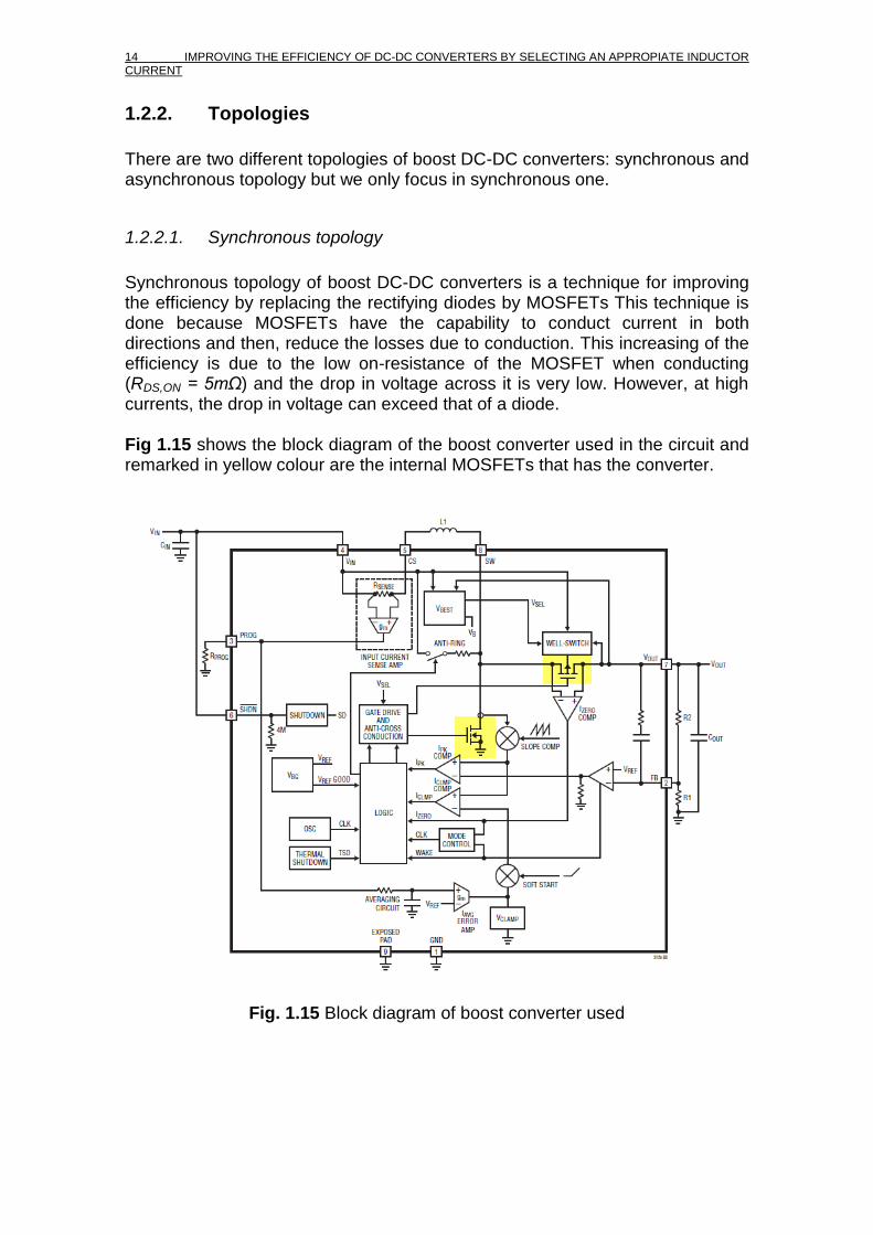
Synchronous topology of boost DC-DC converters is a technique for improving the efficiency by replacing the rectifying diodes by MOSFETs This technique is done because MOSFETs have the capability to conduct current in both directions and then, reduce the losses due to conduction. This increasing of the efficiency is due to the low on-resistance of the MOSFET when conducting (RDS,ON = 5mΩ) and the drop in voltage across it is very low. However, at high currents, the drop in voltage can exceed that of a diode. Fig 1.15 shows the block diagram of the boost converter used in the circuit and remarked in yellow colour are the internal MOSFETs that has the converter.
Fig. 1.15 Block diagram of boost converter used
PROPOSED OPERATING PRINCIPLE 15
CHAPTER 2. PROPOSED OPERATING PRINCIPLE
2.1. Proposal circuit
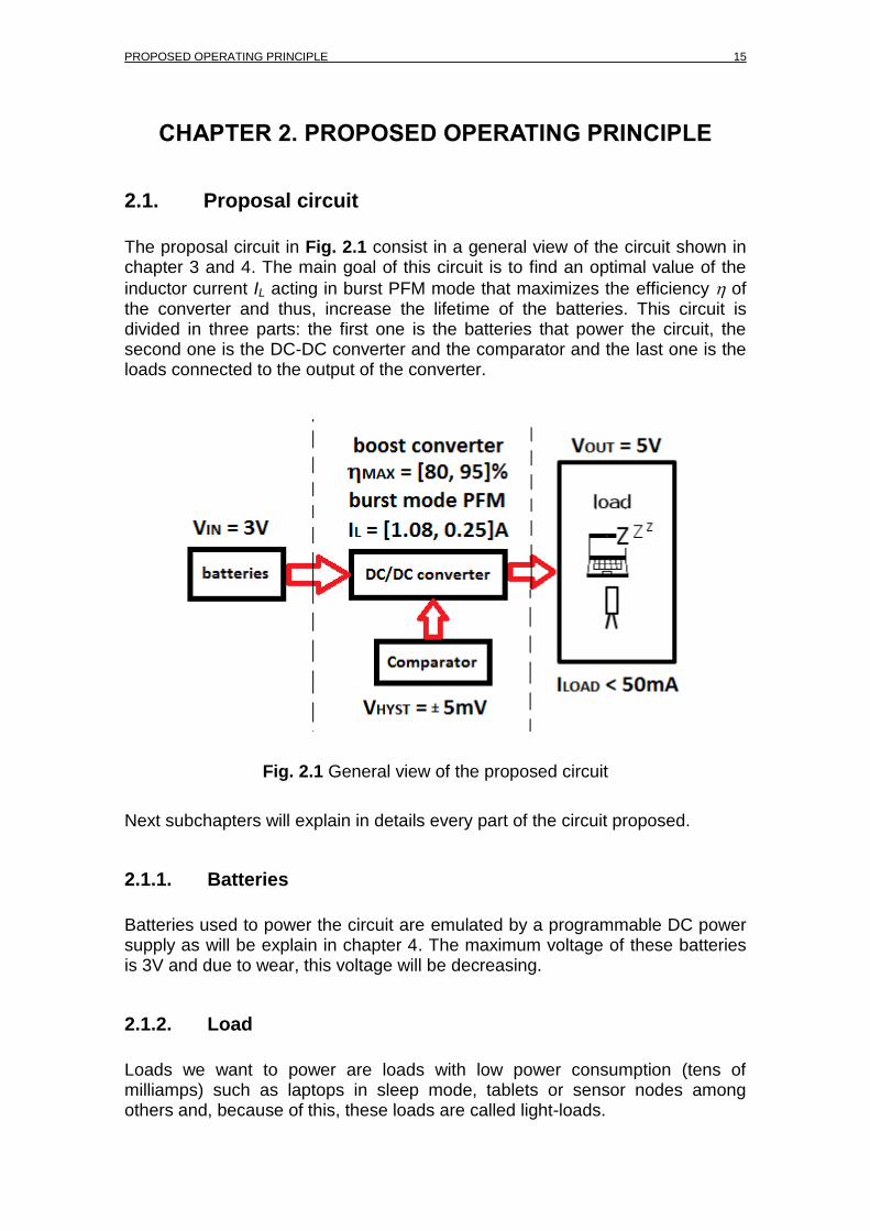
The proposal circuit in Fig. 2.1 consist in a general view of the circuit shown in chapter 3 and 4. The main goal of this circuit is to find an optimal value of the
inductor current IL acting in burst PFM mode that maximizes the efficiency of the converter and thus, increase the lifetime of the batteries. This circuit is divided in three parts: the first one is the batteries that power the circuit, the second one is the DC-DC converter and the comparator and the last one is the loads connected to the output of the converter.
Fig. 2.1 General view of the proposed circuit
Next subchapters will explain in details every part of the circuit proposed.
2.1.1. Batteries
Batteries used to power the circuit are emulated by a programmable DC power supply as will be explain in chapter 4. The maximum voltage of these batteries is 3V and due to wear, this voltage will be decreasing.
2.1.2. Load
Loads we want to power are loads with low power consumption (tens of milliamps) such as laptops in sleep mode, tablets or sensor nodes among others and, because of this, these loads are called light-loads.
16 IMPROVING THE EFFICIENCY OF DC-DC CONVERTERS BY SELECTING AN APPROPIATE INDUCTOR CURRENT
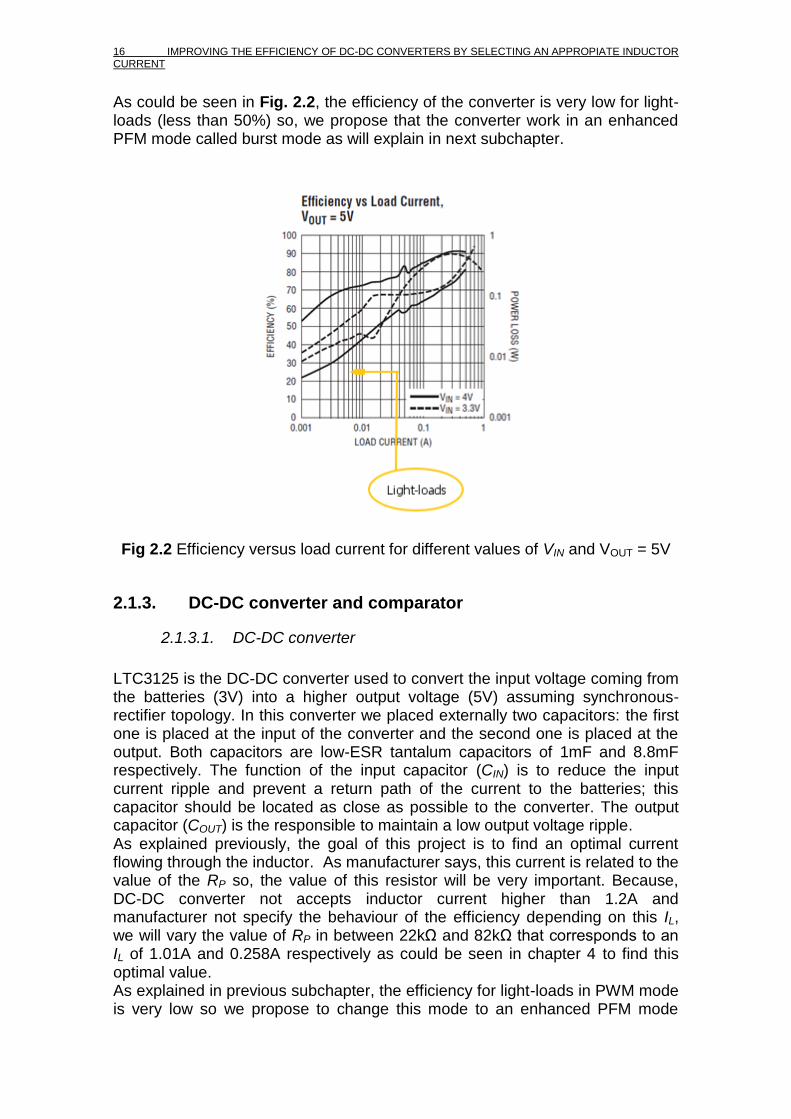
As could be seen in Fig. 2.2, the efficiency of the converter is very low for light-loads (less than 50%) so, we propose that the converter work in an enhanced PFM mode called burst mode as will explain in next subchapter.
Fig 2.2 Efficiency versus load current for different values of VIN and VOUT = 5V
2.1.3. DC-DC converter and comparator
2.1.3.1. DC-DC converter
LTC3125 is the DC-DC converter used to convert the input voltage coming from the batteries (3V) into a higher output voltage (5V) assuming synchronous-rectifier topology. In this converter we placed externally two capacitors: the first one is placed at the input of the converter and the second one is placed at the output. Both capacitors are low-ESR tantalum capacitors of 1mF and 8.8mF respectively. The function of the input capacitor (CIN) is to reduce the input current ripple and prevent a return path of the current to the batteries; this capacitor should be located as close as possible to the converter. The output capacitor (COUT) is the responsible to maintain a low output voltage ripple. As explained previously, the goal of this project is to find an optimal current flowing through the inductor. As manufacturer says, this current is related to the value of the RP so, the value of this resistor will be very important. Because, DC-DC converter not accepts inductor current higher than 1.2A and manufacturer not specify the behaviour of the efficiency depending on this IL, we will vary the value of RP in between 22kΩ and 82kΩ that corresponds to an IL of 1.01A and 0.258A respectively as could be seen in chapter 4 to find this optimal value. As explained in previous subchapter, the efficiency for light-loads in PWM mode is very low so we propose to change this mode to an enhanced PFM mode

PROPOSED OPERATING PRINCIPLE 17
called burst mode and the efficiency will increase. This mode consists in send a burst of pulses when the converter is activated and stops sending the burst pulses when the converter is deactivated. This activating and deactivating of the converter is done in order to save battery and increase the battery lifetime. On the other hand, manufacturer says that this converter is able to convert input voltage from 1.8V to 5.5V into a higher output voltage from 2V to 5.25V but, we try it under our conditions (VIN = 3V and VOUT = 5V) and not works properly. We do not know the reason of this behaviour. Because of this reason, we put an external comparator to realise this comparison as explain in the next subsection.
2.1.3.2. Comparator
This comparator has to consume very low power not to affect too much to the final efficiency so we choose LTC1440 because is an ultra-low power comparator. This comparator is responsible for obtaining the desired hysteresis voltage (±5mV) by connecting a pair of resistors in the comparator according to the explained configuration in chapter 3. The output of the comparator is connected to the feedback pin of the converter in order to know if the converter must enter in ON state or in OFF state.
2.2. Power losses and efficiency
A DC-DC converter has three different types of power losses in active mode: fixed losses, conduction losses and switching losses, so the total DC-DC converter power loss can be expressed as: PL,ACTIVE = PCOND + PSWITCH + PFIX (2.1)
where PFIX are the fixed losses due to the current consumed by the load and not depends on the switching frequency. PCOND are the conduction losses mainly generated by Joule effect involved in the parasitic resistance and are directly dependent on the load current and independent of switching frequency and PSWITCH are the switching losses generated by the switching of the DC-DC converter. On the other hand, in inactive mode there are only fixed losses: PL,INACTIVE = PFIX (2.2)
The overall losses are the sum of the losses due to inactive mode and active mode is:
18 IMPROVING THE EFFICIENCY OF DC-DC CONVERTERS BY SELECTING AN APPROPIATE INDUCTOR CURRENT
PLOSS = PL,ACTIVE + 𝑃𝐿,𝐼𝑁𝐴𝐶𝑇𝐼𝑉𝐸 (2.3)
Combining eq. 2.1 and eq. 2.2 in eq. 2.3 we obtain the overall losses of the circuit as: PLOSS = PCOND,active + PSWITCH,active + PFIX,active + 𝑃𝐹𝐼𝑋,𝑖𝑛𝑎𝑐𝑡𝑖𝑣𝑒 (2.4)
a) Fixed losses As can be seen in eq. 2.4, fixed losses can be divided in two parts: fixed losses in active mode and fixed losses in inactive mode. The fixed losses in active mode can be expressed as: PFIX = 𝑉𝑂𝑈𝑇 ∙ 𝐼𝐿,𝑎𝑐𝑡𝑖𝑣𝑒 (2.5)
where IL,active is the load current consumed by circuits want to power in active mode. We cannot consider the losses due to the leakage current of the comparator because they are negligible (Ileakage = 10pA) The fixed losses in inactive mode can be expressed as: PFIX = 𝑉𝑂𝑈𝑇 ∙ 𝐼𝐿,𝑖𝑛𝑎𝑐𝑡𝑖𝑣𝑒 (2.6)
where IL,inactive is the load current consumed by circuits want to power in inactive mode. This load current is expected to be smaller than IL,active. b) Conduction losses Conduction losses in active mode can be expresses as:
PCOND = 𝑅𝐸𝑄 ∙ 𝐼𝐿02 (2.7)
where REQ is the equivalent resistance series of the circuit and IL0 is the average current flowing through the inductor.
PROPOSED OPERATING PRINCIPLE 19
c) Switching losses There are two types of switching losses: the first one is due to the charge and discharge parasitic capacitances of the circuit and the second one is due to the voltage-current overlap in the transitions between the on-state to the off-state and vice versa. The losses due to the charge and discharge can be expressed as:
PSWITCH,1 = 𝐶𝐸𝑄 ∙ 𝑉𝑂𝑈𝑇2 ∙ 𝑓𝑆𝑊 (2.8)
where CEQ is the equivalent capacitance of the whole circuit and fSW is the switching frequency On the other hand, losses due to the voltage-current overlap can be expressed as: PSWITCH,2 = 𝑉𝑂𝑈𝑇 ∙ 𝐼𝐿0 ∙ 𝑡𝑐 ∙ 𝑓𝑆𝑊 (2.9)
where tc is the average transition time The efficiency of the circuit is:
η =𝑃𝐼𝑁−𝑃𝐿𝑂𝑆𝑆
𝑃𝐼𝑁 (2.10)
where PIN is the input power of the circuit (PIN = VIN·IIN) Taking into account eq. 2.5, eq. 2.6, eq. 2.7, eq. 2.8 and eq. 2.9 that correspond to each power losses involved in the efficiency, we can approximate the overall efficiency of the circuit and find an optimal value of inductor current that maximizes the efficiency and thus, increase the battery lifetime. The expected performance of the efficiency taking into account all previous losses is shown in Fig 2.3.
20 IMPROVING THE EFFICIENCY OF DC-DC CONVERTERS BY SELECTING AN APPROPIATE INDUCTOR CURRENT
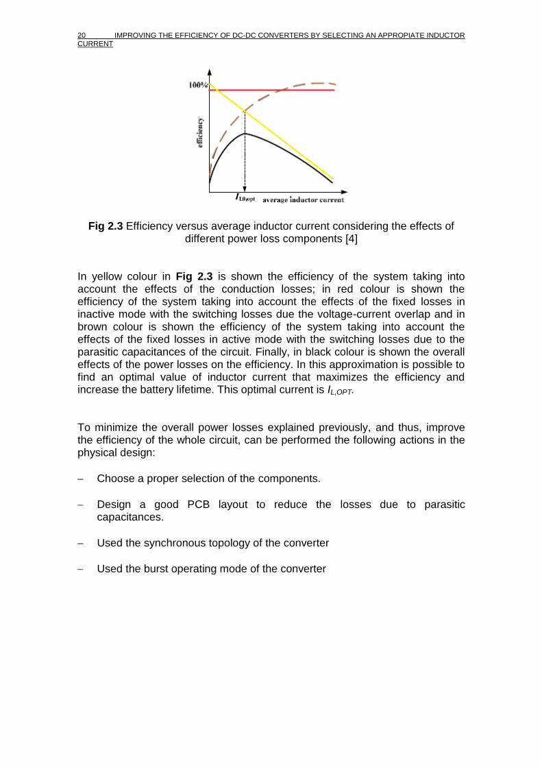
Fig 2.3 Efficiency versus average inductor current considering the effects of different power loss components [4]
In yellow colour in Fig 2.3 is shown the efficiency of the system taking into account the effects of the conduction losses; in red colour is shown the efficiency of the system taking into account the effects of the fixed losses in inactive mode with the switching losses due the voltage-current overlap and in brown colour is shown the efficiency of the system taking into account the effects of the fixed losses in active mode with the switching losses due to the parasitic capacitances of the circuit. Finally, in black colour is shown the overall effects of the power losses on the efficiency. In this approximation is possible to find an optimal value of inductor current that maximizes the efficiency and increase the battery lifetime. This optimal current is IL,OPT. To minimize the overall power losses explained previously, and thus, improve the efficiency of the whole circuit, can be performed the following actions in the physical design:
Choose a proper selection of the components.
Design a good PCB layout to reduce the losses due to parasitic capacitances.
Used the synchronous topology of the converter
Used the burst operating mode of the converter

SIMULATIONS 21
CHAPTER 3. SIMULATIONS This chapter will take a closer look into the software responsible to simulate the whole circuit designed, the software LTspice IV. Afterward, the comparator circuit LTC1440 and the DC-DC converter circuit LTC125 are explained and finally, a simulation of the whole circuit with ideal situations will be done.
3.1. Simulation software
The software used to simulate the circuit is “LTspice IV” manufactured by Linear Technology Corporation. The software is freeware computer implementing SPICE simulator of electronic circuits and was developed to simulate analog circuits fast enough to make simulation of complex SMPS systems.
3.1.1. Hardware requirements
LTspice IV can run on any PC with Windows 98 or above and on Linux is only tested on Linux RedHat 8.0 with WINE version 20030219 platform. Manufacturer recommends that PC has free hard disk space >10GB because simulations can generate many MB of data in a few period of time and large amount of RAM (>1GB), [5].
3.2. Circuit design
The whole design circuit is divided in two different circuits: the first circuit is an ultralow power comparator with a voltage reference (LTC1440) and the second circuit is a synchronous boost DC-DC converter with input current limit and high efficiency (LTC3125). In the designed circuit, we selected an inductor of L =
4.7H, an output capacitor of COUT = 8.8mF and an input capacitor CIN = 1mF. Fig 3.1 shows the whole used circuit in LTspice IV software
22 IMPROVING THE EFFICIENCY OF DC-DC CONVERTERS BY SELECTING AN APPROPIATE INDUCTOR CURRENT
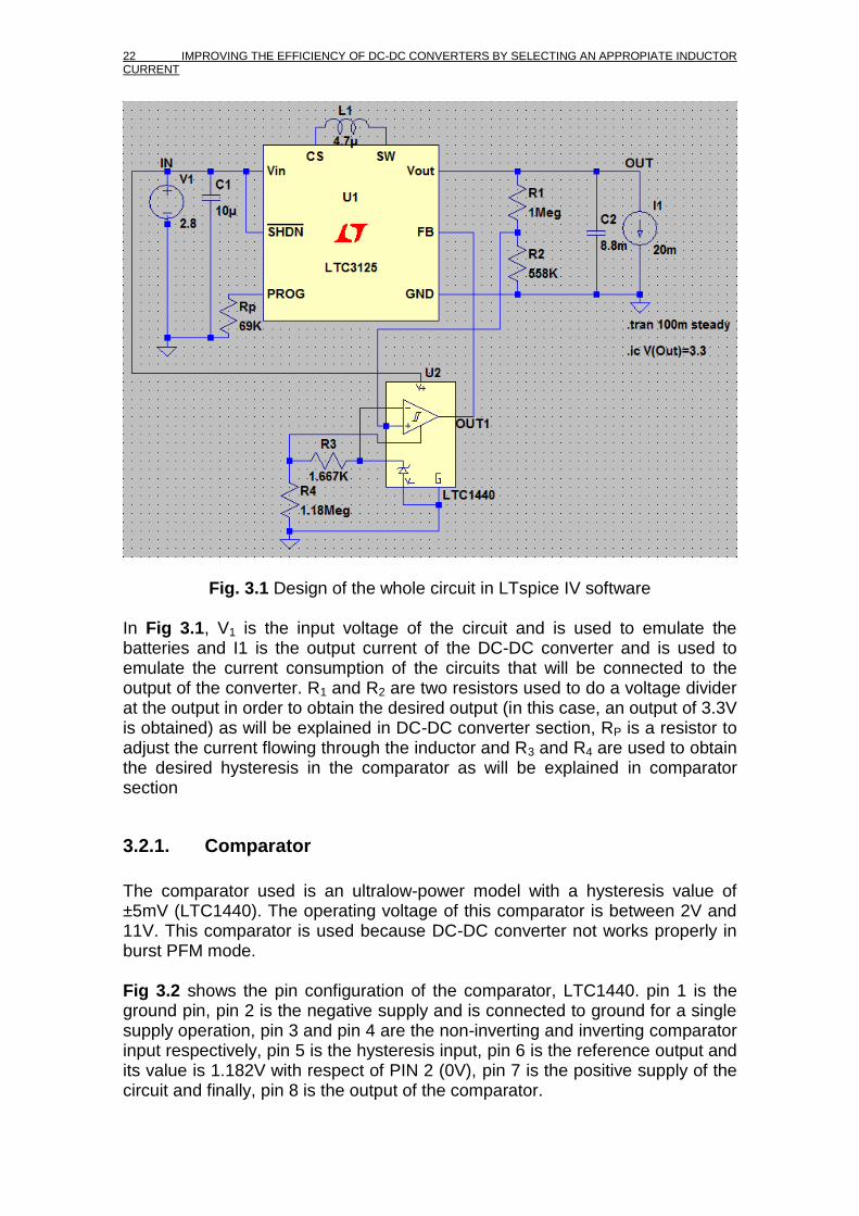
Fig. 3.1 Design of the whole circuit in LTspice IV software In Fig 3.1, V1 is the input voltage of the circuit and is used to emulate the batteries and I1 is the output current of the DC-DC converter and is used to emulate the current consumption of the circuits that will be connected to the output of the converter. R1 and R2 are two resistors used to do a voltage divider at the output in order to obtain the desired output (in this case, an output of 3.3V is obtained) as will be explained in DC-DC converter section, RP is a resistor to adjust the current flowing through the inductor and R3 and R4 are used to obtain the desired hysteresis in the comparator as will be explained in comparator section
3.2.1. Comparator
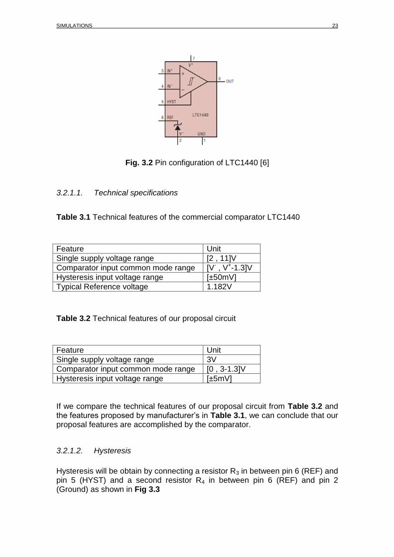
The comparator used is an ultralow-power model with a hysteresis value of ±5mV (LTC1440). The operating voltage of this comparator is between 2V and 11V. This comparator is used because DC-DC converter not works properly in burst PFM mode. Fig 3.2 shows the pin configuration of the comparator, LTC1440. pin 1 is the ground pin, pin 2 is the negative supply and is connected to ground for a single supply operation, pin 3 and pin 4 are the non-inverting and inverting comparator input respectively, pin 5 is the hysteresis input, pin 6 is the reference output and its value is 1.182V with respect of PIN 2 (0V), pin 7 is the positive supply of the circuit and finally, pin 8 is the output of the comparator.
SIMULATIONS 23
Fig. 3.2 Pin configuration of LTC1440 [6]
3.2.1.1. Technical specifications
Table 3.1 Technical features of the commercial comparator LTC1440
Feature Unit
Single supply voltage range [2 , 11]V
Comparator input common mode range [V- , V+-1.3]V
Hysteresis input voltage range [±50mV]
Typical Reference voltage 1.182V
Table 3.2 Technical features of our proposal circuit
Feature Unit
Single supply voltage range 3V
Comparator input common mode range [0 , 3-1.3]V
Hysteresis input voltage range [±5mV]
If we compare the technical features of our proposal circuit from Table 3.2 and the features proposed by manufacturer’s in Table 3.1, we can conclude that our proposal features are accomplished by the comparator.
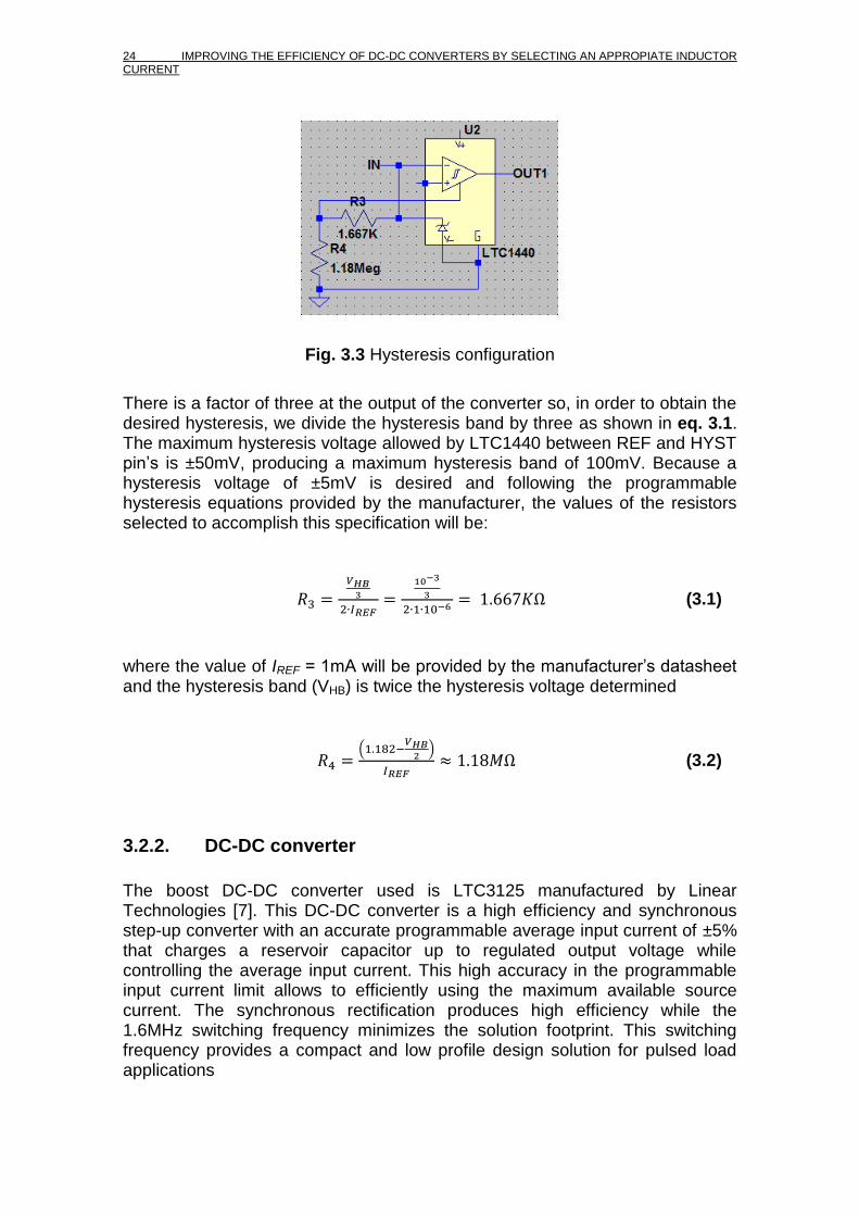
3.2.1.2. Hysteresis
Hysteresis will be obtain by connecting a resistor R3 in between pin 6 (REF) and pin 5 (HYST) and a second resistor R4 in between pin 6 (REF) and pin 2 (Ground) as shown in Fig 3.3
24 IMPROVING THE EFFICIENCY OF DC-DC CONVERTERS BY SELECTING AN APPROPIATE INDUCTOR CURRENT
Fig. 3.3 Hysteresis configuration
There is a factor of three at the output of the converter so, in order to obtain the desired hysteresis, we divide the hysteresis band by three as shown in eq. 3.1. The maximum hysteresis voltage allowed by LTC1440 between REF and HYST pin’s is ±50mV, producing a maximum hysteresis band of 100mV. Because a hysteresis voltage of ±5mV is desired and following the programmable hysteresis equations provided by the manufacturer, the values of the resistors selected to accomplish this specification will be:
𝑅3 =𝑉𝐻𝐵
3
2∙𝐼𝑅𝐸𝐹=
10−3
3
2∙1∙10−6 = 1.667𝐾Ω (3.1)
where the value of IREF = 1mA will be provided by the manufacturer’s datasheet and the hysteresis band (VHB) is twice the hysteresis voltage determined
𝑅4 =(1.182−
𝑉𝐻𝐵2
)
𝐼𝑅𝐸𝐹≈ 1.18𝑀Ω (3.2)
3.2.2. DC-DC converter
The boost DC-DC converter used is LTC3125 manufactured by Linear Technologies [7]. This DC-DC converter is a high efficiency and synchronous step-up converter with an accurate programmable average input current of ±5% that charges a reservoir capacitor up to regulated output voltage while controlling the average input current. This high accuracy in the programmable input current limit allows to efficiently using the maximum available source current. The synchronous rectification produces high efficiency while the 1.6MHz switching frequency minimizes the solution footprint. This switching frequency provides a compact and low profile design solution for pulsed load applications
SIMULATIONS 25
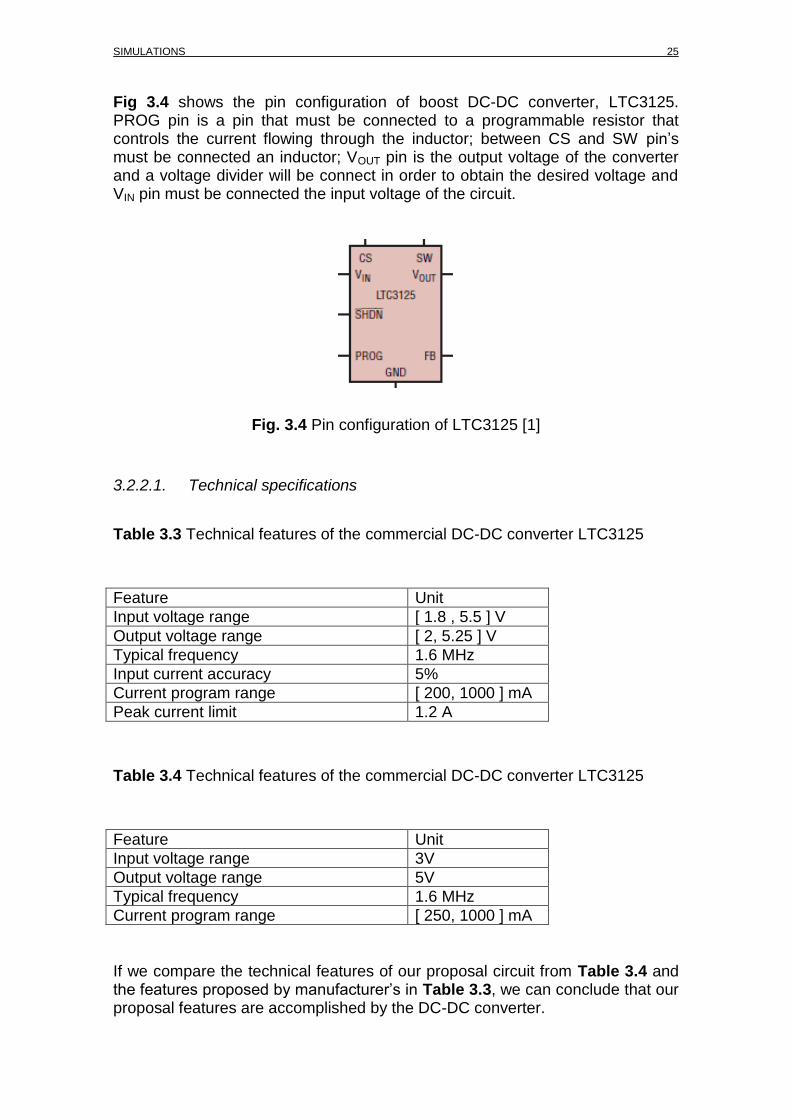
Fig 3.4 shows the pin configuration of boost DC-DC converter, LTC3125. PROG pin is a pin that must be connected to a programmable resistor that controls the current flowing through the inductor; between CS and SW pin’s must be connected an inductor; VOUT pin is the output voltage of the converter and a voltage divider will be connect in order to obtain the desired voltage and VIN pin must be connected the input voltage of the circuit.
Fig. 3.4 Pin configuration of LTC3125 [1]
3.2.2.1. Technical specifications
Table 3.3 Technical features of the commercial DC-DC converter LTC3125
Feature Unit
Input voltage range [ 1.8 , 5.5 ] V
Output voltage range [ 2, 5.25 ] V
Typical frequency 1.6 MHz
Input current accuracy 5%
Current program range [ 200, 1000 ] mA
Peak current limit 1.2 A
Table 3.4 Technical features of the commercial DC-DC converter LTC3125
Feature Unit
Input voltage range 3V
Output voltage range 5V
Typical frequency 1.6 MHz
Current program range [ 250, 1000 ] mA
If we compare the technical features of our proposal circuit from Table 3.4 and the features proposed by manufacturer’s in Table 3.3, we can conclude that our proposal features are accomplished by the DC-DC converter.

26 IMPROVING THE EFFICIENCY OF DC-DC CONVERTERS BY SELECTING AN APPROPIATE INDUCTOR CURRENT
3.2.2.2. Output voltage
To obtain the desired output voltage, a voltage divider must be connected at the output of the DC-DC converter as shown in Fig. 3.5.
Fig. 3.5 Output resistance voltage divider configuration
To find the values of the resistors R1 and R2 that accomplish the desired voltage will be:
𝑉𝐹𝐵 = 𝑉𝑂𝑈𝑇𝑅2
𝑅1+𝑅2 (3.3)
if R1 = 1MΩ, VOUT = 3.3V and VFB = 1.182V (determined by comparator’s manufacturer), a value of R1 will be determined as:
𝑅2 =𝑅1∙𝑉𝐹𝐵
(𝑉𝑂𝑈𝑇−𝑉𝐹𝐵)=
1∙106∙1.182
(3.3−1.182)≈ 558𝐾Ω (3.4)
3.2.2.3. Programmable resistor
RP is a resistor connected between PROG pin and ground and is the responsible of controlling the current flowing through the inductor. In the experimental design, it is important to place this resistor as close as possible to PROG pin in order to minimize parasitic capacitance and noise pick-up. Because the inductor current can range from 200mA and 1000mA, a set of commercials resistors will be selected. Another important thing that manufacturer says is that the resistor tolerance affects directly to the current limit accuracy but in this design, will not affect.
SIMULATIONS 27
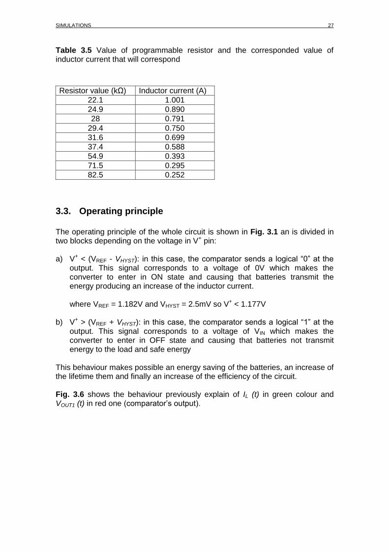
Table 3.5 Value of programmable resistor and the corresponded value of inductor current that will correspond
Resistor value (kΩ) Inductor current (A)
22.1 1.001
24.9 0.890
28 0.791
29.4 0.750
31.6 0.699
37.4 0.588
54.9 0.393
71.5 0.295
82.5 0.252
3.3. Operating principle
The operating principle of the whole circuit is shown in Fig. 3.1 an is divided in two blocks depending on the voltage in V+ pin: a) V+ < (VREF - VHYST): in this case, the comparator sends a logical “0” at the
output. This signal corresponds to a voltage of 0V which makes the converter to enter in ON state and causing that batteries transmit the energy producing an increase of the inductor current. where VREF = 1.182V and VHYST = 2.5mV so V+ < 1.177V
b) V+ > (VREF + VHYST): in this case, the comparator sends a logical “1” at the output. This signal corresponds to a voltage of VIN which makes the converter to enter in OFF state and causing that batteries not transmit energy to the load and safe energy
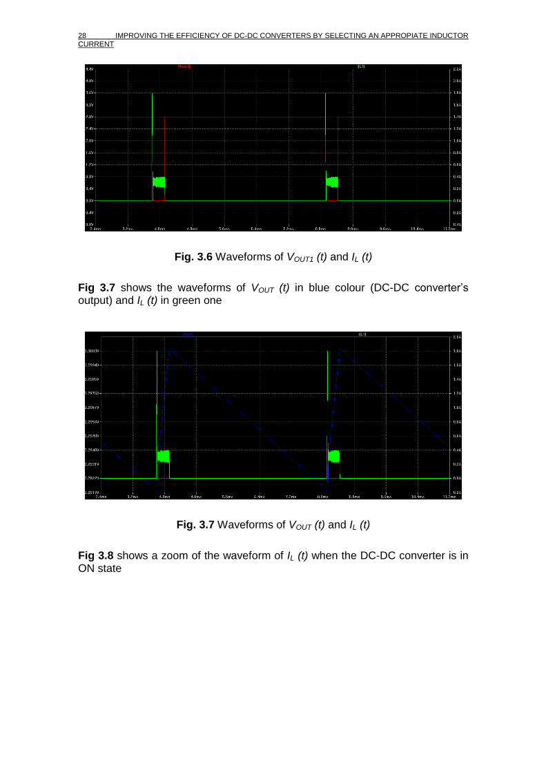
This behaviour makes possible an energy saving of the batteries, an increase of the lifetime them and finally an increase of the efficiency of the circuit. Fig. 3.6 shows the behaviour previously explain of IL (t) in green colour and VOUT1 (t) in red one (comparator’s output).
28 IMPROVING THE EFFICIENCY OF DC-DC CONVERTERS BY SELECTING AN APPROPIATE INDUCTOR CURRENT
Fig. 3.6 Waveforms of VOUT1 (t) and IL (t)
Fig 3.7 shows the waveforms of VOUT (t) in blue colour (DC-DC converter’s output) and IL (t) in green one
Fig. 3.7 Waveforms of VOUT (t) and IL (t)
Fig 3.8 shows a zoom of the waveform of IL (t) when the DC-DC converter is in ON state
SIMULATIONS 29
Fig. 3.8 Zoom in the waveforms of IL (t)
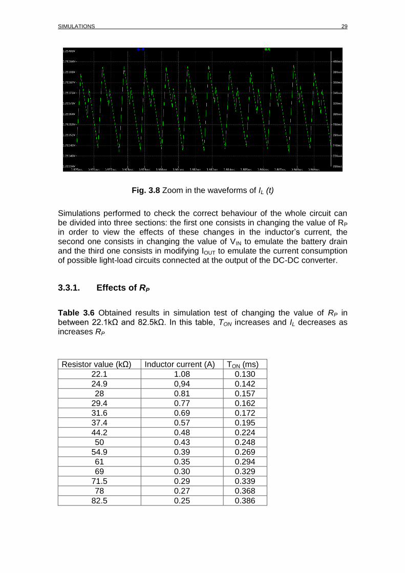
Simulations performed to check the correct behaviour of the whole circuit can be divided into three sections: the first one consists in changing the value of RP in order to view the effects of these changes in the inductor’s current, the second one consists in changing the value of VIN to emulate the battery drain and the third one consists in modifying IOUT to emulate the current consumption of possible light-load circuits connected at the output of the DC-DC converter.
3.3.1. Effects of RP
Table 3.6 Obtained results in simulation test of changing the value of RP in between 22.1kΩ and 82.5kΩ. In this table, TON increases and IL decreases as increases RP
Resistor value (kΩ) Inductor current (A) TON (ms)
22.1 1.08 0.130
24.9 0,94 0.142
28 0.81 0.157
29.4 0.77 0.162
31.6 0.69 0.172
37.4 0.57 0.195
44.2 0.48 0.224
50 0.43 0.248
54.9 0.39 0.269
61 0.35 0.294
69 0.30 0.329
71.5 0.29 0.339
78 0.27 0.368
82.5 0.25 0.386
30 IMPROVING THE EFFICIENCY OF DC-DC CONVERTERS BY SELECTING AN APPROPIATE INDUCTOR CURRENT
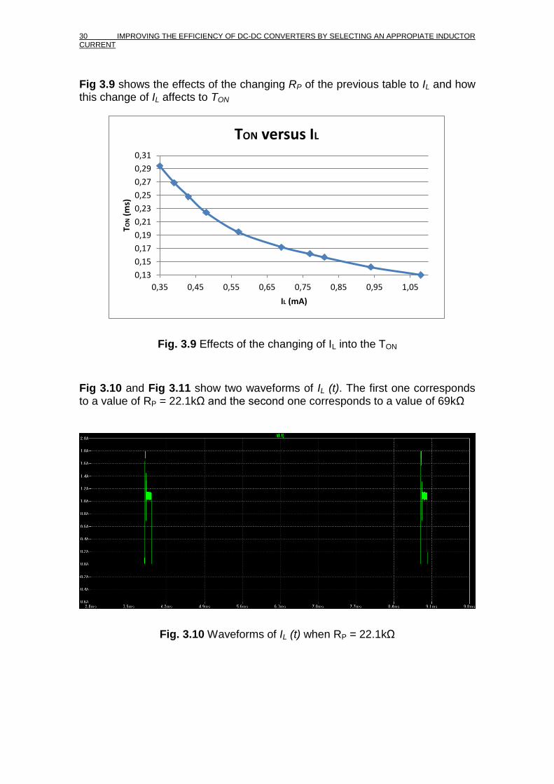
Fig 3.9 shows the effects of the changing RP of the previous table to IL and how this change of IL affects to TON
Fig. 3.9 Effects of the changing of IL into the TON
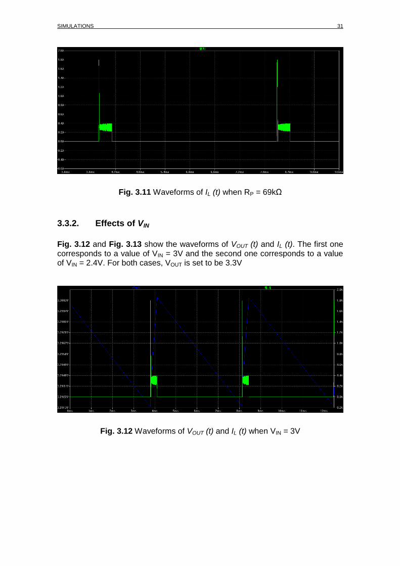
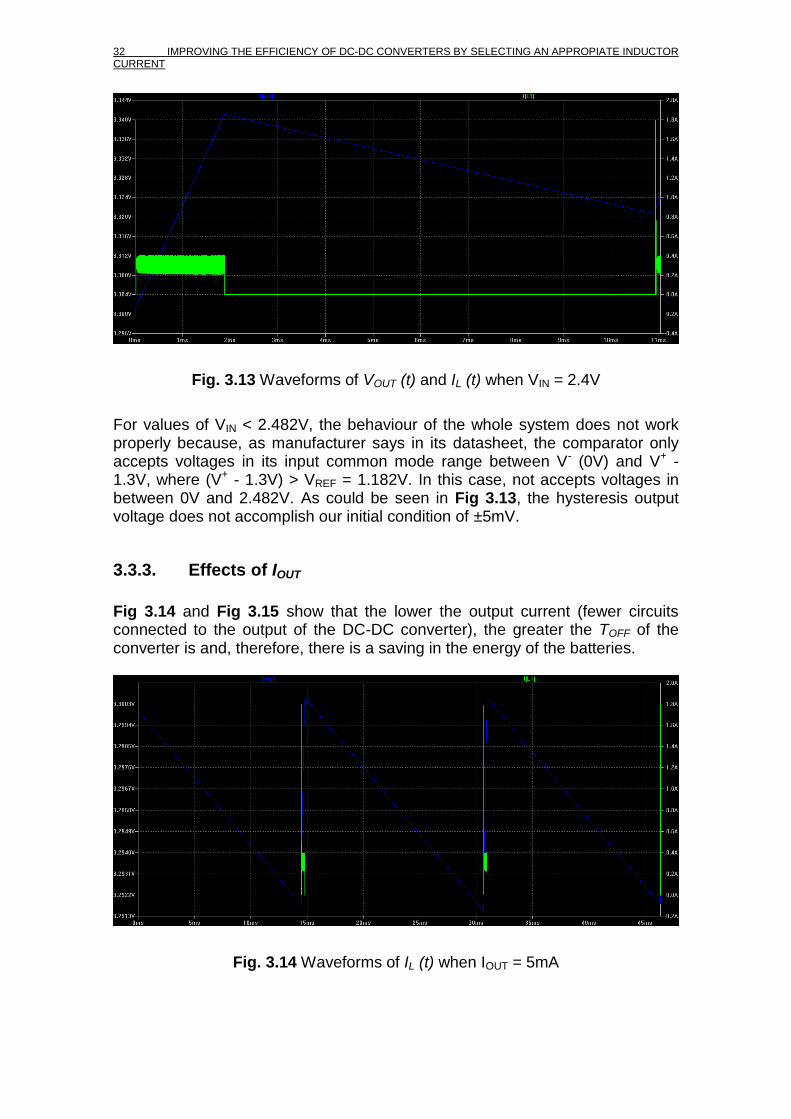
Fig 3.10 and Fig 3.11 show two waveforms of IL (t). The first one corresponds to a value of RP = 22.1kΩ and the second one corresponds to a value of 69kΩ
Fig. 3.10 Waveforms of IL (t) when RP = 22.1kΩ
0,13
0,15
0,17
0,19
0,21
0,23
0,25
0,27
0,29
0,31
0,35 0,45 0,55 0,65 0,75 0,85 0,95 1,05
TON
(m
s)
IL (mA)
TON versus IL
SIMULATIONS 31
Fig. 3.11 Waveforms of IL (t) when RP = 69kΩ
3.3.2. Effects of VIN
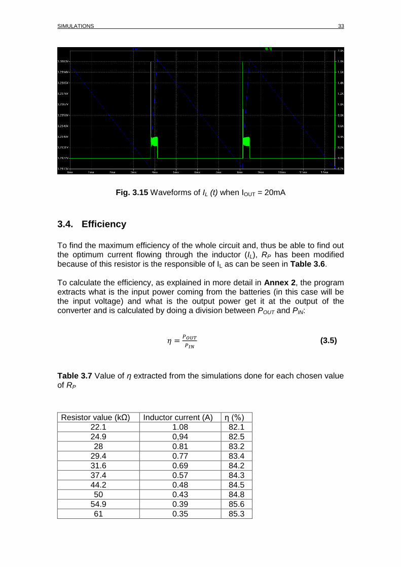
Fig. 3.12 and Fig. 3.13 show the waveforms of VOUT (t) and IL (t). The first one corresponds to a value of VIN = 3V and the second one corresponds to a value of VIN = 2.4V. For both cases, VOUT is set to be 3.3V
Fig. 3.12 Waveforms of VOUT (t) and IL (t) when VIN = 3V
32 IMPROVING THE EFFICIENCY OF DC-DC CONVERTERS BY SELECTING AN APPROPIATE INDUCTOR CURRENT
Fig. 3.13 Waveforms of VOUT (t) and IL (t) when VIN = 2.4V
For values of VIN < 2.482V, the behaviour of the whole system does not work properly because, as manufacturer says in its datasheet, the comparator only accepts voltages in its input common mode range between V- (0V) and V+ -1.3V, where (V+ - 1.3V) > VREF = 1.182V. In this case, not accepts voltages in between 0V and 2.482V. As could be seen in Fig 3.13, the hysteresis output voltage does not accomplish our initial condition of ±5mV.
3.3.3. Effects of IOUT
Fig 3.14 and Fig 3.15 show that the lower the output current (fewer circuits connected to the output of the DC-DC converter), the greater the TOFF of the converter is and, therefore, there is a saving in the energy of the batteries.
Fig. 3.14 Waveforms of IL (t) when IOUT = 5mA
SIMULATIONS 33
Fig. 3.15 Waveforms of IL (t) when IOUT = 20mA
3.4. Efficiency
To find the maximum efficiency of the whole circuit and, thus be able to find out the optimum current flowing through the inductor (IL), RP has been modified because of this resistor is the responsible of IL as can be seen in Table 3.6. To calculate the efficiency, as explained in more detail in Annex 2, the program extracts what is the input power coming from the batteries (in this case will be the input voltage) and what is the output power get it at the output of the converter and is calculated by doing a division between POUT and PIN:
𝜂 =𝑃𝑂𝑈𝑇
𝑃𝐼𝑁 (3.5)
Table 3.7 Value of η extracted from the simulations done for each chosen value of RP
Resistor value (kΩ) Inductor current (A) η (%)
22.1 1.08 82.1
24.9 0,94 82.5
28 0.81 83.2
29.4 0.77 83.4
31.6 0.69 84.2
37.4 0.57 84.3
44.2 0.48 84.5
50 0.43 84.8
54.9 0.39 85.6
61 0.35 85.3

34 IMPROVING THE EFFICIENCY OF DC-DC CONVERTERS BY SELECTING AN APPROPIATE INDUCTOR CURRENT
69 0.30 85.7
71.5 0.29 85.2
78 0.27 85
82.5 0.25 84.8
Fig 3.16 shows the efficiency obtained versus IL. An optimal value of this current is obtained (IOPT = 300mA) and a maximum efficiency of η = 85.7%
Fig. 3.16 Efficiency versus IL (t) when VIN = 2.8V, VOUT = 3.3V and IOUT = 20mA
Table 3.8 Efficiency report of power dissipated by each element if RP = 22.1kΩ
Efficiency report
Efficiency: 81.3%
Input: 81.1mW @2.8V
Output: 65,9mW @3.3V
Ref. IRMS (mA) IPEAK (mA) Dissipation (mW)
C1 0 0 0
C2 155 1773 0
L1 189 1796 0
R1 0 0 0.4
R2 0 0 0.2
R3 0 0 0
R4 0 0 0.1
RP 0 0 0.2
U1 189 1823 15
U2 0 0 0
81,5
82
82,5
83
83,5
84
84,5
85
85,5
86
0,25 0,45 0,65 0,85 1,05
(
%)
IL (mA)
SIMULATIONS 35
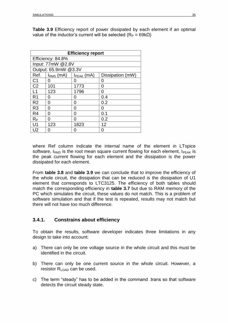
Table 3.9 Efficiency report of power dissipated by each element if an optimal value of the inductor’s current will be selected (RP = 69kΩ)
Efficiency report
Efficiency: 84.8%
Input: 77mW @2.8V
Output: 65.9mW @3.3V
Ref. IRMS (mA) IPEAK (mA) Dissipation (mW)
C1 0 0 0
C2 101 1773 0
L1 123 1796 0
R1 0 0 0.4
R2 0 0 0.2
R3 0 0 0
R4 0 0 0.1
RP 0 0 0.2
U1 123 1823 12
U2 0 0 0
where Ref column indicate the internal name of the element in LTspice software, IRMS is the root mean square current flowing for each element, IPEAK is the peak current flowing for each element and the dissipation is the power dissipated for each element. From table 3.8 and table 3.9 we can conclude that to improve the efficiency of the whole circuit, the dissipation that can be reduced is the dissipation of U1 element that corresponds to LTC3125. The efficiency of both tables should match the corresponding efficiency in table 3.7 but due to RAM memory of the PC which simulates the circuit, these values do not match. This is a problem of software simulation and that if the test is repeated, results may not match but there will not have too much difference.
3.4.1. Constrains about efficiency
To obtain the results, software developer indicates three limitations in any design to take into account: a) There can only be one voltage source in the whole circuit and this must be
identified in the circuit.
b) There can only be one current source in the whole circuit. However, a resistor RLOAD can be used.
c) The term “steady” has to be added in the command .trans so that software detects the circuit steady state.
36 IMPROVING THE EFFICIENCY OF DC-DC CONVERTERS BY SELECTING AN APPROPIATE INDUCTOR CURRENT
CHAPTER 4. EXPERIMENTAL ANALYSIS This chapter explains the materials used in the set-up configuration, the method used to obtain the efficiency of the circuit and finally the results of these tests and the maximum efficiency find and the optimal inductor current obtained that makes possible the maximum efficiency previously mentioned.
4.1. Materials & method
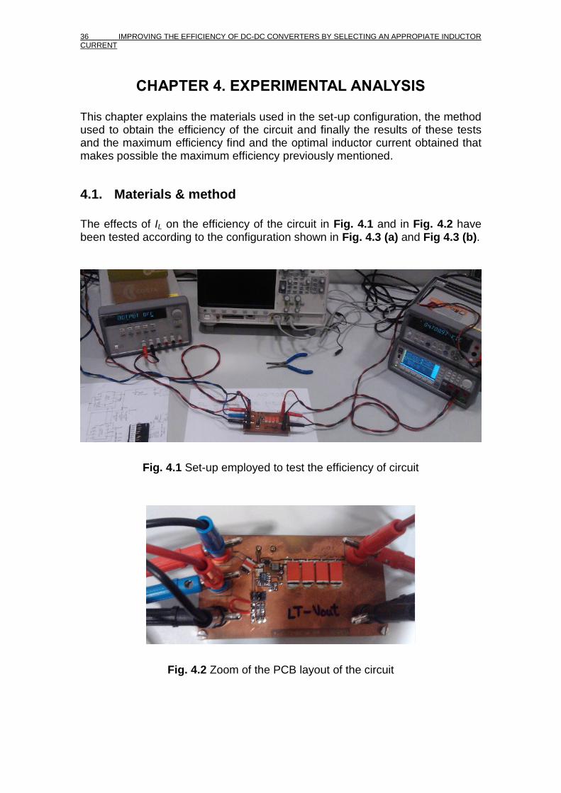
The effects of IL on the efficiency of the circuit in Fig. 4.1 and in Fig. 4.2 have been tested according to the configuration shown in Fig. 4.3 (a) and Fig 4.3 (b).
Fig. 4.1 Set-up employed to test the efficiency of circuit
Fig. 4.2 Zoom of the PCB layout of the circuit
EXPERIMENTAL ANALYSIS 37
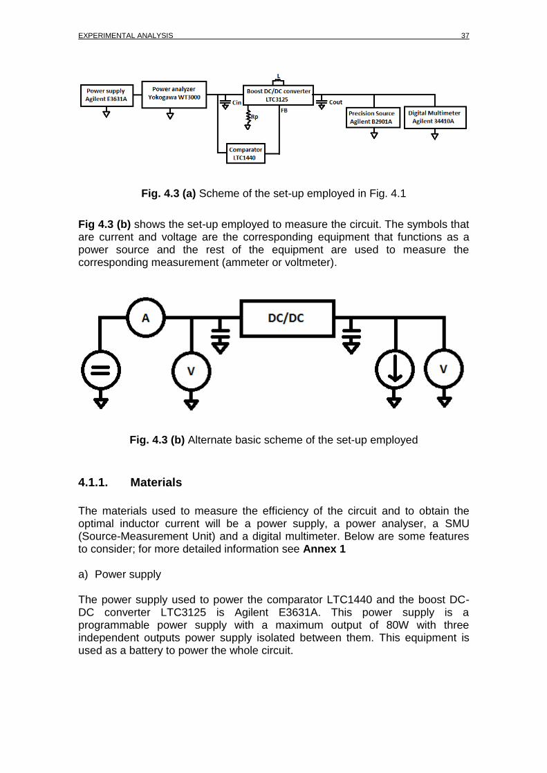
Fig. 4.3 (a) Scheme of the set-up employed in Fig. 4.1
Fig 4.3 (b) shows the set-up employed to measure the circuit. The symbols that are current and voltage are the corresponding equipment that functions as a power source and the rest of the equipment are used to measure the corresponding measurement (ammeter or voltmeter).
Fig. 4.3 (b) Alternate basic scheme of the set-up employed
4.1.1. Materials
The materials used to measure the efficiency of the circuit and to obtain the optimal inductor current will be a power supply, a power analyser, a SMU (Source-Measurement Unit) and a digital multimeter. Below are some features to consider; for more detailed information see Annex 1 a) Power supply The power supply used to power the comparator LTC1440 and the boost DC-DC converter LTC3125 is Agilent E3631A. This power supply is a programmable power supply with a maximum output of 80W with three independent outputs power supply isolated between them. This equipment is used as a battery to power the whole circuit.
38 IMPROVING THE EFFICIENCY OF DC-DC CONVERTERS BY SELECTING AN APPROPIATE INDUCTOR CURRENT
b) Power analyser The power analyser used to measure the input power of the circuit is Yokogawa WT3000. This power analyser has a high accuracy, a wide frequency range and a data update rate between 50ms and 20s. This equipment is used to measure the input power and has been configured with a measuring time of 5s and a sampling frequency of 200kSa/s c) SMU The SMU used to emulate the circuits that could be connected to the output of the DC-DC converter is Agilent B2901A. This SMU has a high resolution, the capability to measure voltage and current and a maximum sample rate of 50000 points/s. This equipment is used as a current source in the circuit and has been limited with an input current to 2A. d) Digital multimeter The digital multimeter used to measure the output voltage of the DC-DC converter in order to estimate the output power multiplying this voltage by the output current selected on the precision source is Agilent 34410A. The integration time of this equipment has been configured as 2s.
4.1.2. Method
The method used to obtain the efficiency report and, thus the optimal current flowing through the inductor is:
Configure the measuring instruments
Interconnect each measuring instrument to the corresponding circuit connection as could be seen in Fig 4.1
Turn-on the power supply and later DMM
Measure PIN, VOUT and POUT
4.1.2.1. Input power
The measurement of PIN is done with the power analyser equipment. To measure this value, only is necessary to view the displayed power value that shows the power analyser in his display and, later do an average of 10 obtained values to obtain a more reliable value.
EXPERIMENTAL ANALYSIS 39
4.1.2.2. Output voltage
The measurement of VOUT is done with the DMM equipment. To obtain the measured value only is necessary to view the displayed value that shows the DMM’s display. Because of the instrument’s accuracy, an average of 10 obtained values has been carried out to obtain a more reliable value. To change the value of VOUT, only is necessary to change the resistors of the voltage divider connected to the output of the boost DC-DC converter. In this case, VOUT only can be changed to three different voltages (4V, 5V and 5.5V).
4.1.2.3. Output current
The value of IOUT is always fixed on the SMU equipment because it acts as a source. All tests are realised with three different output current values (5 mA, 10 mA and 20 mA).
4.1.2.4. Output power
The measurement of POUT is done manually and is necessary to multiply the IOUT by VOUT obtained previously. Eq. 4.1 is used to obtain the output power of the circuit:
𝑃𝑂𝑈𝑇 = 𝑉𝑂𝑈𝑇 ∙ 𝐼𝑂𝑈𝑇 (4.1)
4.2. Efficiency
The measurement of η is calculated by the division of the output power and the input power as shown in eq. 4.2.
Ƞ =𝑃𝑂𝑈𝑇
𝑃𝐼𝑁 (4.2)
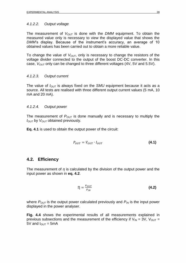
where POUT is the output power calculated previously and PIN is the input power displayed in the power analyser. Fig. 4.4 shows the experimental results of all measurements explained in previous subsections and the measurement of the efficiency if VIN = 3V, VOUT = 5V and IOUT = 5mA
40 IMPROVING THE EFFICIENCY OF DC-DC CONVERTERS BY SELECTING AN APPROPIATE INDUCTOR CURRENT
Fig. 4.4 Experimental results if VIN = 3V, VOUT = 5V and IOUT = 5mA
To view the behaviour of the efficiency depending of the critical changed values, IOUT, VIN and VOUT, three different tests have been done: the first one is to change the value of IOUT and maintain VIN and VOUT at a constant value, the second one is to change the value of VIN and maintain IOUT and VOUT at a constant value and the last test is to change the value of VOUT and maintain IOUT and VIN at a constant value.
4.2.1. Effects of IOUT
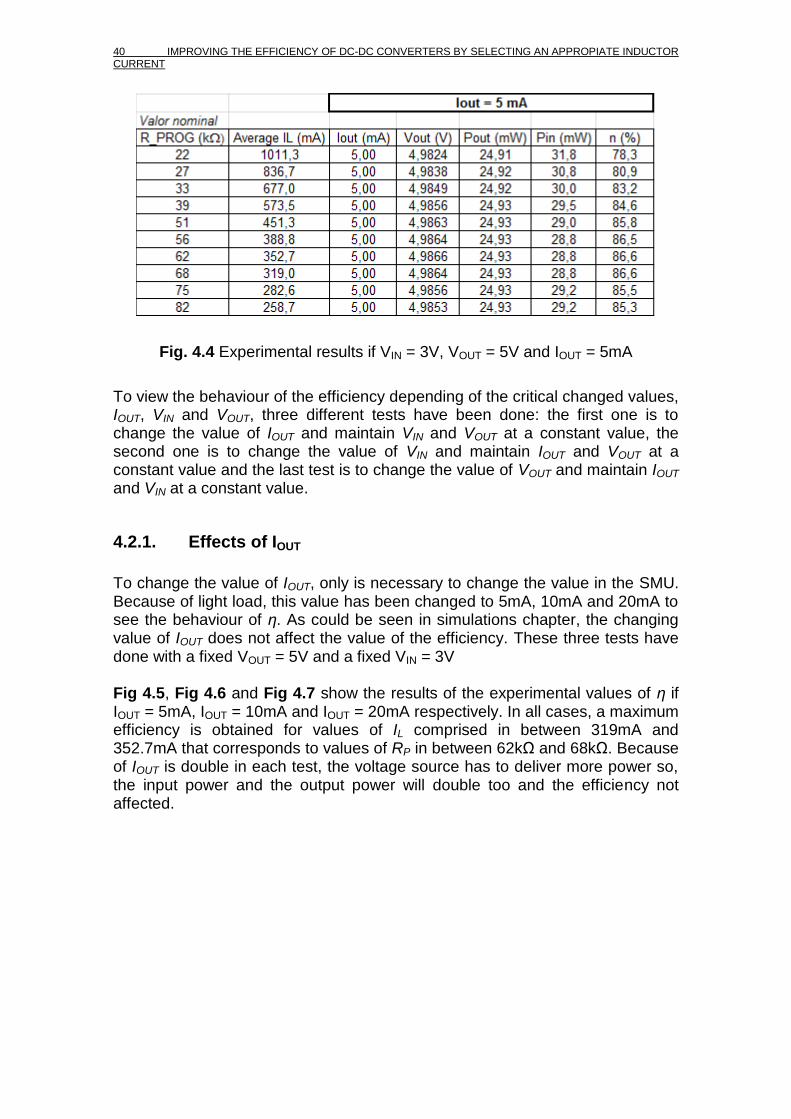
To change the value of IOUT, only is necessary to change the value in the SMU. Because of light load, this value has been changed to 5mA, 10mA and 20mA to see the behaviour of η. As could be seen in simulations chapter, the changing value of IOUT does not affect the value of the efficiency. These three tests have done with a fixed VOUT = 5V and a fixed VIN = 3V Fig 4.5, Fig 4.6 and Fig 4.7 show the results of the experimental values of η if IOUT = 5mA, IOUT = 10mA and IOUT = 20mA respectively. In all cases, a maximum efficiency is obtained for values of IL comprised in between 319mA and 352.7mA that corresponds to values of RP in between 62kΩ and 68kΩ. Because of IOUT is double in each test, the voltage source has to deliver more power so, the input power and the output power will double too and the efficiency not affected.
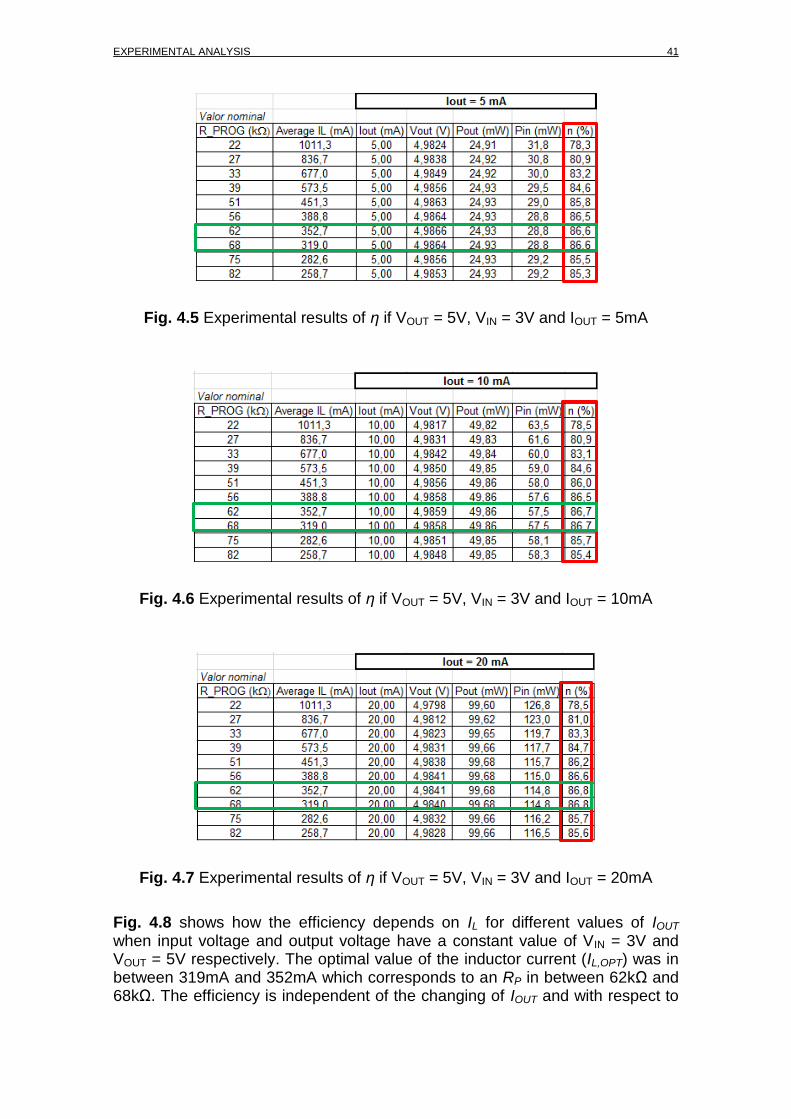
EXPERIMENTAL ANALYSIS 41
Fig. 4.5 Experimental results of η if VOUT = 5V, VIN = 3V and IOUT = 5mA
Fig. 4.6 Experimental results of η if VOUT = 5V, VIN = 3V and IOUT = 10mA
Fig. 4.7 Experimental results of η if VOUT = 5V, VIN = 3V and IOUT = 20mA
Fig. 4.8 shows how the efficiency depends on IL for different values of IOUT when input voltage and output voltage have a constant value of VIN = 3V and VOUT = 5V respectively. The optimal value of the inductor current (IL,OPT) was in between 319mA and 352mA which corresponds to an RP in between 62kΩ and 68kΩ. The efficiency is independent of the changing of IOUT and with respect to
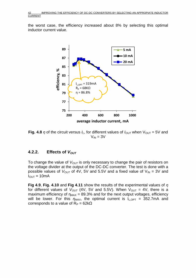
42 IMPROVING THE EFFICIENCY OF DC-DC CONVERTERS BY SELECTING AN APPROPIATE INDUCTOR CURRENT
the worst case, the efficiency increased about 8% by selecting this optimal inductor current value.
Fig. 4.8 η of the circuit versus IL, for different values of IOUT when VOUT = 5V and VIN = 3V
4.2.2. Effects of VOUT
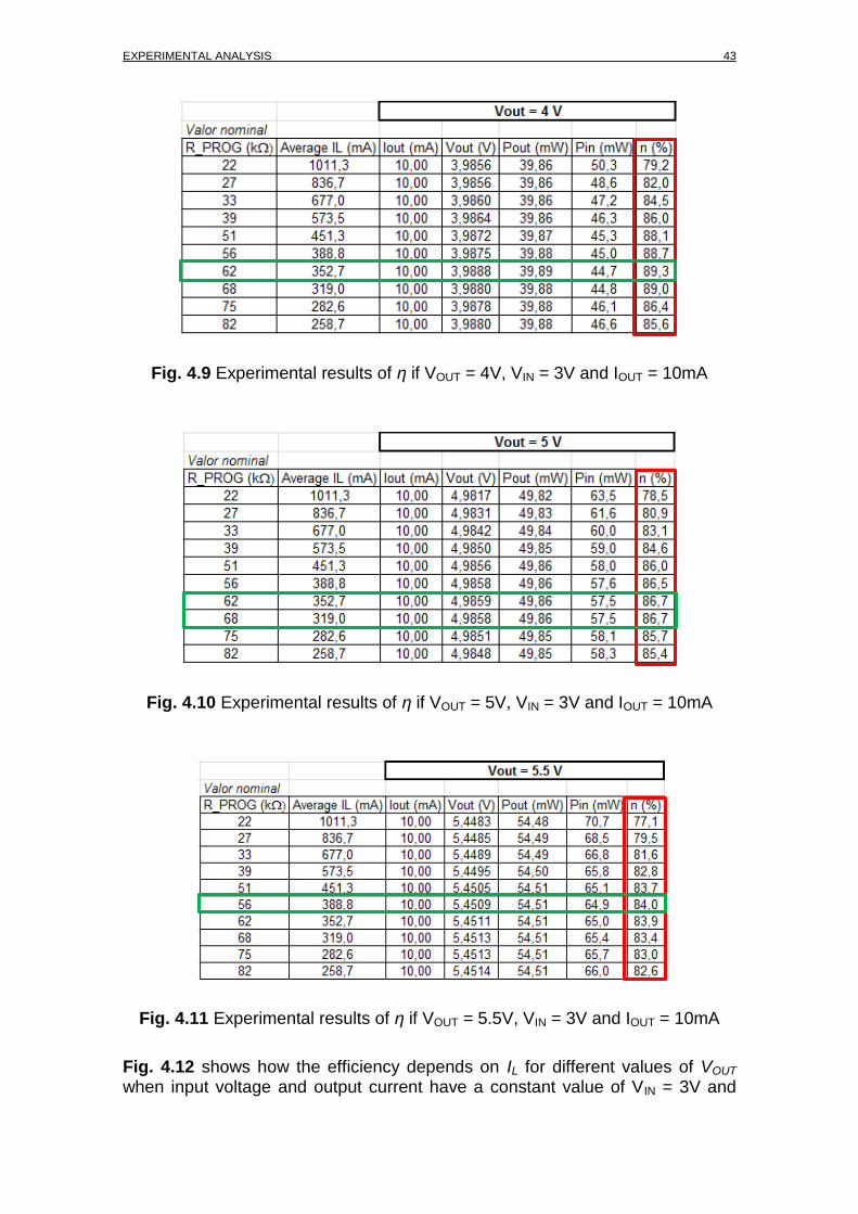
To change the value of VOUT is only necessary to change the pair of resistors on the voltage divider at the output of the DC-DC converter. The test is done with a possible values of VOUT of 4V, 5V and 5.5V and a fixed value of VIN = 3V and IOUT = 10mA Fig 4.9, Fig. 4.10 and Fig 4.11 show the results of the experimental values of η for different values of VOUT (4V, 5V and 5.5V). When VOUT = 4V, there is a maximum efficiency of ηMAX = 89.3% and for the next output voltages, efficiency will be lower. For this ηMAX, the optimal current is IL,OPT = 352.7mA and corresponds to a value of RP = 62kΩ
75
77
79
81
83
85
87
89
200 400 600 800 1000
effi
cien
cy,
%
average inductor current, mA
5 mA
10 mA
20 mA
IL,OPT = 319mA RP = 68KΩ η = 86.8%
EXPERIMENTAL ANALYSIS 43
Fig. 4.9 Experimental results of η if VOUT = 4V, VIN = 3V and IOUT = 10mA
Fig. 4.10 Experimental results of η if VOUT = 5V, VIN = 3V and IOUT = 10mA
Fig. 4.11 Experimental results of η if VOUT = 5.5V, VIN = 3V and IOUT = 10mA
Fig. 4.12 shows how the efficiency depends on IL for different values of VOUT when input voltage and output current have a constant value of VIN = 3V and
44 IMPROVING THE EFFICIENCY OF DC-DC CONVERTERS BY SELECTING AN APPROPIATE INDUCTOR CURRENT
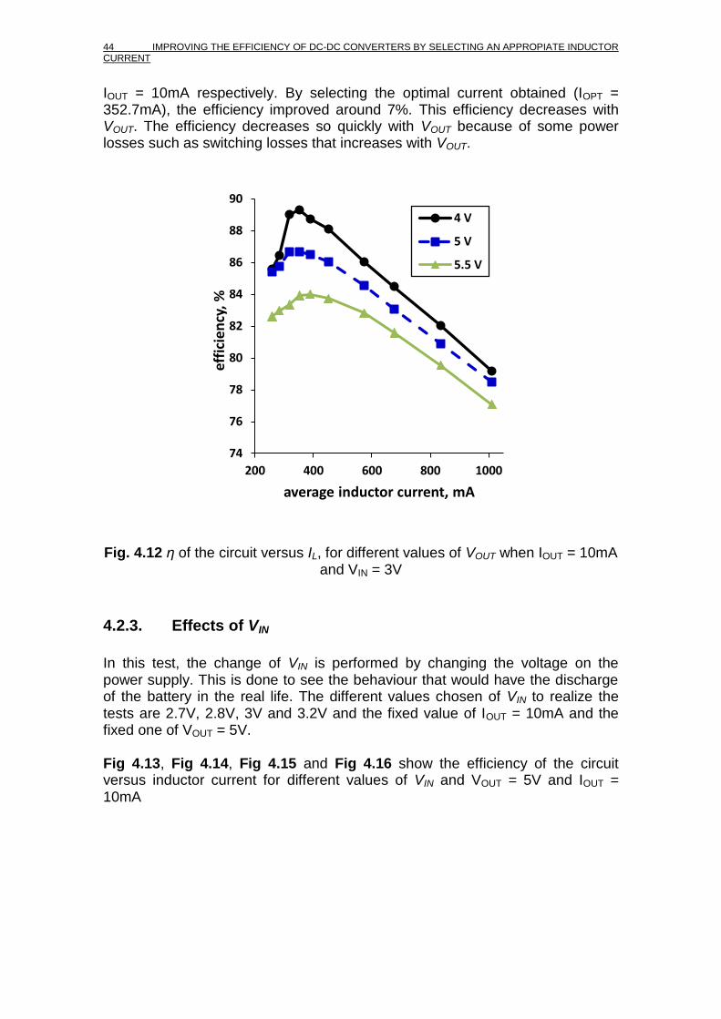
IOUT = 10mA respectively. By selecting the optimal current obtained (IOPT = 352.7mA), the efficiency improved around 7%. This efficiency decreases with VOUT. The efficiency decreases so quickly with VOUT because of some power losses such as switching losses that increases with VOUT.
Fig. 4.12 η of the circuit versus IL, for different values of VOUT when IOUT = 10mA and VIN = 3V
4.2.3. Effects of VIN
In this test, the change of VIN is performed by changing the voltage on the power supply. This is done to see the behaviour that would have the discharge of the battery in the real life. The different values chosen of VIN to realize the tests are 2.7V, 2.8V, 3V and 3.2V and the fixed value of IOUT = 10mA and the fixed one of VOUT = 5V. Fig 4.13, Fig 4.14, Fig 4.15 and Fig 4.16 show the efficiency of the circuit versus inductor current for different values of VIN and VOUT = 5V and IOUT = 10mA
74
76
78
80
82
84
86
88
90
200 400 600 800 1000
effi
cien
cy,
%
average inductor current, mA
4 V
5 V
5.5 V

EXPERIMENTAL ANALYSIS 45
Fig. 4.13 Experimental results of η if VIN = 2.7V, VOUT = 5V and IOUT = 10mA
Fig. 4.14 Experimental results of η if VIN = 2.8V, VOUT = 5V and IOUT = 10mA
Fig. 4.15 Experimental results of η if VIN = 3V, VOUT = 5V and IOUT = 10mA

46 IMPROVING THE EFFICIENCY OF DC-DC CONVERTERS BY SELECTING AN APPROPIATE INDUCTOR CURRENT
Fig. 4.16 Experimental results of η if VIN = 3.2V, VOUT = 5V and IOUT = 10mA
Fig 4.17 shows how the efficiency depends on IL for different values of VIN when output voltage and output current have a constant value of VOUT = 5V and IOUT = 10mA respectively. For value of VIN in between 2.7V and 3V, the optimal inductor current remains significantly constant at a value of IL,OPT = 352.7mA and for values higher than 3V, seems that the optimal inductor current (IL,OPT) should increase with the increasing of VIN.
Fig. 4.17 Efficiency of the circuit versus IL, for different values of VIN when IOUT = 10mA and VOUT = 5V
For values of VIN between 2.7V and 3.2V, IL,OPT goes from 352mA to 389mA. In the best case (VIN = 2.7V) and selecting this optimal current, the efficiency will
75
77
79
81
83
85
87
89
200 400 600 800 1000
effi
cie
ncy
, %
average inductor current, mA
2.7 V
2.8 V
3 V
3.2 V

EXPERIMENTAL ANALYSIS 47
increase up to 9.2% with respect to the worst case. This improving efficiency by selecting the optimal current also decreases with the increasing of VIN as can be seen in Table 4.1
Table 4.1. Δη of the whole system for different values of VIN
VIN (V) Δη (%)
2.7 9.2
2.8 8.8
3 8.3
3.2 7.6

48 IMPROVING THE EFFICIENCY OF DC-DC CONVERTERS BY SELECTING AN APPROPIATE INDUCTOR CURRENT
CONCLUSIONS LTC3125 is a boost DC-DC converter that could work in two different modes: PWM and PFM but in this project we were unable to verify the proper operation in PFM mode and, therefore, we placed an external comparator to force the DC-DC converter working in this mode. Depending on the selected mode, the efficiency could be better or not but, under the conditions of light load, PFM would have higher efficiency than PWM. This efficiency not only depends on the selected mode, it depends too on the power losses that affect to the DC-DC converter. There are three types of power losses such as conduction losses associated to the Joule effect involved in the parasitic resistance and dependent on the load current, switching losses associated to the switching frequency of the DC-DC converter and finally fixed losses that not depends on the switching frequency. A set of experimental test has realised by changing certain critical values such as IOUT, VOUT and VIN to find an optimal inductor current (IL,OPT) that minimizes the power losses. Depending on the critical value changed this IL,OPT can change because of the dependence of this current in the efficiency. If the change occurs in load current (IOUT), this IL,OPT will not be affected because is independent of the IOUT change’s and a value of IL,OPT = 319mA will be obtained
that implies MAX = 86.8%. If the change occurs in VOUT the efficiency is affected increasing with the decreasing of VOUT because power losses increases as
increases VOUT. The maximum efficiency obtained when VOUT = 4V is MAX = 89.3%. Finally, if the change occurs in VIN there is an optimal value of this current (IL,OPT = 352.7mA) for values in between 2.7V and 3V and an optimal value of (IL,OPT = 388.8mA) for VIN = 3.2V so, it seem that IL,OPT increases with
VIN. An efficiency of MAX = 87.5% and MAX = 86.7% are obtained for each case respectively. As shown in LTC3125 datasheet, it has an efficiency of around 40% if PWM mode is selected and work with light load. If the mode is change to burst-mode PFM, DC-DC converter experiments an improvement of the efficiency and can reach values up to 80%. Furthermore, if an optimal inductor current is selected, the efficiency increases more and can reach values up to 89.3%. All tests realised show that if LTC3125 works in burst-mode PFM with an optimal inductor current, the improvement of the efficiency with respect PWM mode is about 49%, thus, the lifetime of the batteries will increase.

REFERENCES 49
REFERENCES [1] Linear Technology. LTC1325. 1.2A synchronous step-up DC/DC converter with input current limit. http://www.linear.com/product/LTC3125 [2] Sengupta, U. PWM and PFM operation of DC-DC converters for portable applications. [3] Keeping, S. The Advantages of Pulse Frequency Modulation for DC/DC Switching Voltage Converters. May, 2014. Hearst Electronic Product http://www.digikey.com/en/articles/techzone/2014/mar/the-advantages-of-pulse-frequency-modulation-for-dc-dc-switching-voltage-converters [4] Reverter, F. and Gasulla, M. Improving the efficiency of PV low-power processing circuits by selecting an optimal inductor current of the DC-DC converter. Eurosensors 2014, Brescia, Italy [5] Linear Technology. LTSpice IV. http://www.linear.com/designtools/software/ [6] Linear Technology. LTC1440. Ultralow power single/dual comparator with reference. http://cds.linear.com/docs/en/datasheet/144012fd.pdf [7] Linear Technology http://www.linear.com/ [8] Agilent Technologies. http://www.keysight.com/main/home.jspx?cc=ES&lc=eng [9] Agilent Technologies. E363xA Series Programmable DC power supplies. http://cp.literature.agilent.com/litweb/pdf/5968-9726EN.pdf [10] Yokogawa. Digital power meter WT300 series. http://tmi.yokogawa.com/files/uploaded/WT300Series_Final.pdf [11] Agilent Technologies. B2900A Series Precision source/measure unit. http://cp.literature.agilent.com/litweb/pdf/5990-7009EN.pdf [12] Agilent Technologies. Agilent 34410A and 34410A Multimeter. http://cp.literature.agilent.com/litweb/pdf/5989-3738EN.pdf [13] Linear Technology. LTSpice Manual. http://ecee.colorado.edu/~mathys/ecen1400/pdf/scad3.pdf
50 IMPROVING THE EFFICIENCY OF DC-DC CONVERTERS BY SELECTING AN APPROPIATE INDUCTOR CURRENT
[14] Werns, M. and Steyaert, M. Basic DC-DC Converter Theory. 2011, Springer. http://www.springer.com/cda/content/document/cda_downloaddocument/9789400714359-c2.pdf?SGWID=0-0-45-1132048-p174109472 [15] Maxim Integrated How to Design an Efficient DC-DC Converter Using the DS1875 PWM Controller. October 2012, Maxim Integrated. http://www.maximintegrated.com/en/app-notes/index.mvp/id/4332 [16] Laurier, S. Experimental analysis of photovoltaic energy scavengers for sensor nodes. 2006, Ghent, Belgium. [17] Erickson, R. and Maksimovic, D. High Efficiency DC-DC converter for battery-operated Systems. Power Electronics Specialists Conf., Atlanta, GA, 1995 [18] Duka, I. and Noble, C. High Efficiency DC/DC Boost Converter. April 2011, Worcester, England https://www.wpi.edu/Pubs/E-project/Available/E-project-042711-220800/unrestricted/High_Frequency_DC_DC_Boost_Converter_MQP_Final_Duka_Noble.pdf [19] Gurbuz, Y., Parlak, M. and Sahin, E. High-Efficiency Low-Voltage DC-DC Conversion for portable Applications using VLSI circuits – ASIC approach. Istanbul, Turkey http://www.researchgate.net/publication/237632431_High-Efficiency_Low-Voltage_DC-DC_Conversion_for_Portable_Applications_using_VLSI_circuits_-_ASIC_approach [20] Sourdif, T. Compact Power Solution Overcomes Peak Power Limitations in PCMCIA-Based Pulsed-Load GSM and GPRS Applications. June 2008. Linear Technology Magazine http://cds.linear.com/docs/en/lt-journal/LTMag-V18N2-aa-LTC3125-Tim_Sourdif.pdf [21] Maxim Integrated. DC-DC converter tutorial. November 2001 http://pdfserv.maximintegrated.com/en/an/AN2031.pdf [22] Slobodan, M. Modelling, analysis and design of switching converters. November 1976. California Institute of Technology http://thesis.library.caltech.edu/1157/1/Cuk_sm_1977.pdf [23] Mohan, N. Power electronics. A first course. Novembre 2011. John Wiley & Sons, Inc. [24] Kosmatin, P., Petkovsek, M. and Voncina, D. High-efficiency DC/DC converter for low-voltage applications. 2010, Ljubljana, Slovenia [25] van Dijk, E., J. N. Spruijt, H., M. O’sullivan, D. and Ben Klaassens, J. PWM-Switch modelling of DC-DC converters. November 1995. IEEExplorer
REFERENCES 51
http://ieeexplore.ieee.org/xpl/login.jsp?tp=&arnumber=471285&url=http%3A%2F%2Fieeexplore.ieee.org%2Fxpls%2Fabs_all.jsp%3Farnumber%3D471285 [26] TOREX. Basics of DC/DC Converters. 2011. Springer www.springer.com [27] Yokogawa. Precision power analyser WT3000. http://tmi.yokogawa.com/products/digital-power-analyzers/digital-power-analyzers/wt3000-precision-power-analyzer/ [28] Linear Technology. Synchronous Rectification in High-Performance Power Converter Design. Texas Instruments 2001. Dallas, Texas http://www.ti.com/lit/an/snva595/snva595.pdf [29] Vishay Siliconix. DC-to-DC design guide. Visahy October 2002. http://www.vishay.com/docs/71917/71917.pdf [30] Bell, B. and Lee, E. Boost Power Converters Finally Get Some Respect!. Texas Instruments June 2013, Phoenix, Arizona [31] Rincon-Mora, G. and Keskar, N. Unscrambling the power losses in switching boost converters. August 2006. IEEExplorer
52 IMPROVING THE EFFICIENCY OF DC-DC CONVERTERS BY SELECTING AN APPROPIATE INDUCTOR CURRENT
ABBREVIATONS AC Alternating Current DC Direct Current SMPS Switching-Mode Power Supply IL Inductor current VOUT Output voltage PWM Pulse Width Modulation PFM Pulse Frequency Modulation L Inductor C Capacitor R Resistor D Duty Cycle TON On-time TOFF Off-time T Period of the pulse VIN Input voltage ID Diode current RDS,ON On-resistance of the MOSFET PLOSS Power loss PCOND Power losses due to conduction loss PSWITCH Power due to switching of converter PFIX Power losses due to fixed losses RAM Random-Access Memory COUT Output capacitor CIN Input capacitor VFB Feedback voltage of the converter VHYST Hysteresis voltage VREF Voltage reference VOUT1 Output voltage of the comparator IIN Input current at the DC-DC converter IOUT Output current at the converter IL,OPT Inductor current IRMS Root Mean Square current RP Programmable resistor η Efficiency PIN Input power POUT Output power EMI Electro Magnetic Interference PC Personal Computer DMM Digital Multimeter SMU Source-Measurement Unit CMRR Common Mode Rejection Ratio
ANNEX 1. MATERIALS 53
ANNEX 1. MATERIALS This annex explains the main specifications of all used materials in the whole circuit.
1.1. Boost DC-DC converter LTC3125
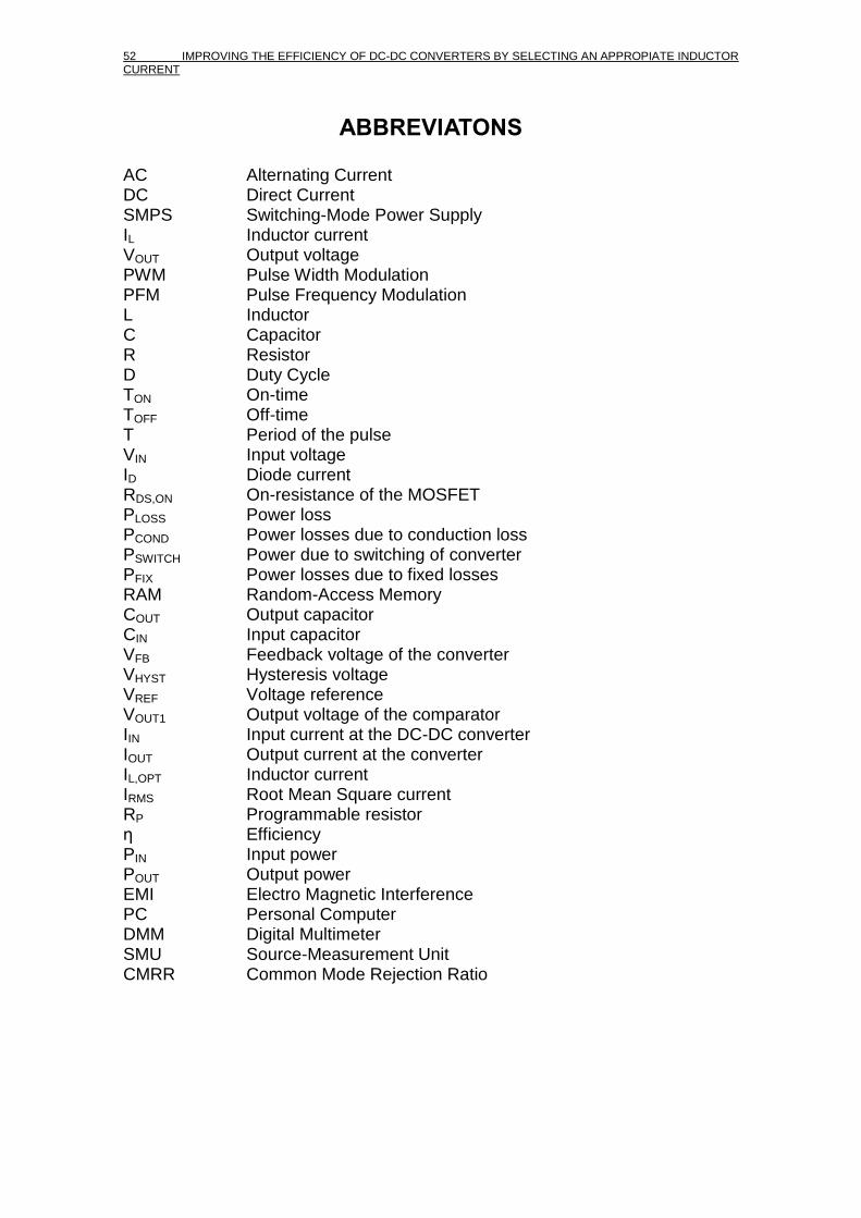
The commercial boost DC-DC converter used is LTC3125. This DC-DC converter is a high efficiency and a synchronous step-up DC-DC converter with an accurate programmable input current limit. This DC-DC converter has an internal oscillator that sets the switching frequency to 1.6MHz. As could be seen previously, the efficiency of the DC-DC converter depends on the load current as follows
Fig. 1.1 Efficiency versus load current for different VIN and VOUT = 5V [1]
Table 1.1 Features of the boost DC-DC converter LTC3125
Feature Unit
Input current accuracy 5%
Average input current range [200 – 1000] mA
Input voltage range [1.8 – 5.5] V
Output voltage range [2 – 5.25] V
Frequency operation 1.6MHz
Peak current limit 1.2A
Efficiency < 93%
feedback voltage [1.176 – 1.229] V
54 IMPROVING THE EFFICIENCY OF DC-DC CONVERTERS BY SELECTING AN APPROPIATE INDUCTOR CURRENT
Maximum duty cycle (VFB = 1.15 V) [ 85 – 92] %
Maximum duty cycle (VFB = 1.3 V) 0 %
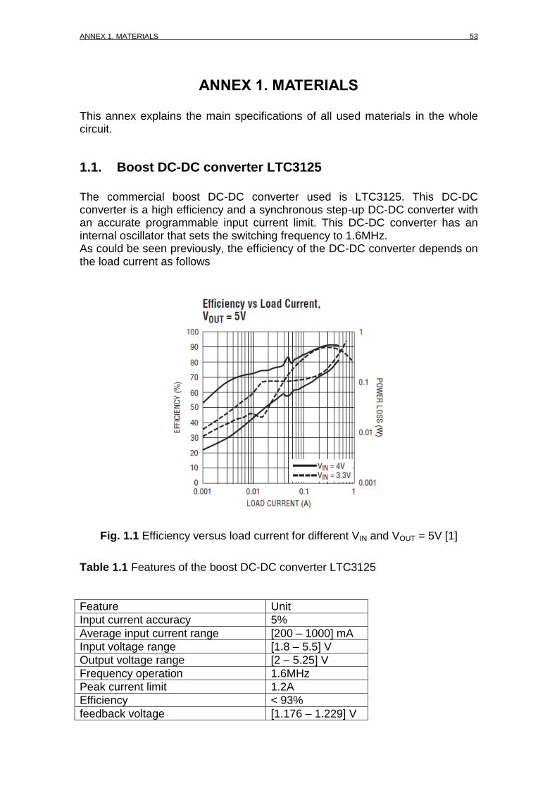
Fig 1.2 shows the average input current limit versus RP with the values proportioned by the manufacturer in its datasheet [1]
Fig. 1.2 Average inductor current versus programmable resistor
1.2. Comparator LTC1440
The commercial comparator used is an ultralow power single comparator with a voltage reference of 1.182V ±1%, a programmable hysteresis. The comparator operates from the negative supply to the positive supply minus 1.3V. This comparator can be used as a level detector by creating a voltage divider from VIN to the non-inverting comparator input (V+) Table 1.2 Features of the ultra-low comparator LTC1440
Feature Unit
Single Voltage supply range [2 , 11] V
Input leakage current (IN+, IN-) ±0.01nA
Input leakage current (HYST) ±0.02nA
Dual Voltage supply range [±1 , ±5.5] V
Comparator input common mode range [V- , V+ - 1.3] V
Hysteresis input voltage range [VREF-50m , VREF] V
0,000
0,250
0,500
0,750
1,000
1,250
20 30 40 50 60 70 80 90
IL (
A)
RP (KΩ)
IL
ANNEX 1. MATERIALS 55
Typical voltage reference 1.182V
Propagation delay 12s
Bypass capacitor < 0.01F
Voltage noise 100VRMS
1.3. Power supply Agilent E3631A
The commercial power supply used is E3631A and is manufactured by Agilent Technologies [8]. This power supply is used to power the boost DC-DC converter and the comparator; it has a maximum power of 80W with a triple output supply and has an excellent regulation and low noise interference. These three outputs are independent in terms of isolation between them to minimize the interference between circuits. Table 1.3 Features of the programmable power supply Agilent E3631A [9]
Feature Unit
DC output voltage [0 – 6] V [0 – 25] V [-25 – 0] V
DC output current [0 – 5] A [0 – 1] A [0 – 1] A
Measure resolution 1mV / 1mA
Transient response < 50 s
1.4. Power analyser Yokogawa WT3000
Power analyser used is Yokogawa WT3000 and is manufactured by Yokogawa [10]. This power analyser is a high accuracy and wide frequency range power analyser It has a low power factor error and is used to measure the power delivered to the circuit that later will be used to calculate the efficiency. Table 1.4 Features of the power analyser Yokogawa WT3000
Feature Unit
Power accuracy 0.02% reading + 0.4% of range
Input current 2A
DC frequency range 0.1Hz to 1MHz
Sampling Frequency ≈ 200KS/s
Guaranteed accuracy range for voltage and current range
1% to 130%
Data update rate 50ms to 20s
56 IMPROVING THE EFFICIENCY OF DC-DC CONVERTERS BY SELECTING AN APPROPIATE INDUCTOR CURRENT
Power factor error 0.03% reading
1.5. SMU Agilent B2901A
SMU used is B2901A and is manufactured by Agilent Technologies [8]. This SMU equipment combines the capabilities of measure voltage and current simultaneously. It has a broad voltage and current sourcing capability, high precision and high measurement throughput. It is used to emulate the possible current which might be consumed by the circuits connected at the output of the DC-DC converter. Table 1.5 Features of the SMU Agilent B2901A [11]
Feature Unit
Output voltage [6 – 210]V
Output current [0.105 - 3.03]A
Maximum output power 31.8W
Maximum sample rate 50000pts/s
Noise 3mVRMS
1.6. Digital Multimeter Agilent 34410A
DMM used is 34410A and is manufactured by Agilent Technologies [8]. This DMM is used to known the output voltage of the DC-DC converter in order to later calculate the efficiency of the converter following eq. 1
𝜂 =𝑃𝑂𝑈𝑇
𝑃𝐼𝑁=
𝑉𝑂𝑈𝑇∙𝐼𝑂𝑈𝑇
𝑃𝐼𝑁 (1)
where VOUT is measured in DMM equipment, IOUT is set in SMU equipment and PIN is measured in power analyser equipment. This DMM has a high performance (high accuracy and high throughput among others) Table 1.6 Features of the DMM Agilent 34410A [12]
Feature Unit
DC voltage range 0.1V, 1V, 10V, 100V, 1000V
DC current range 100A, 1mA, 10mA, 1A, 3A
DC CMRR 140 dB
Accuracy (% reading + % range) 0.0002% + 0.0001% range
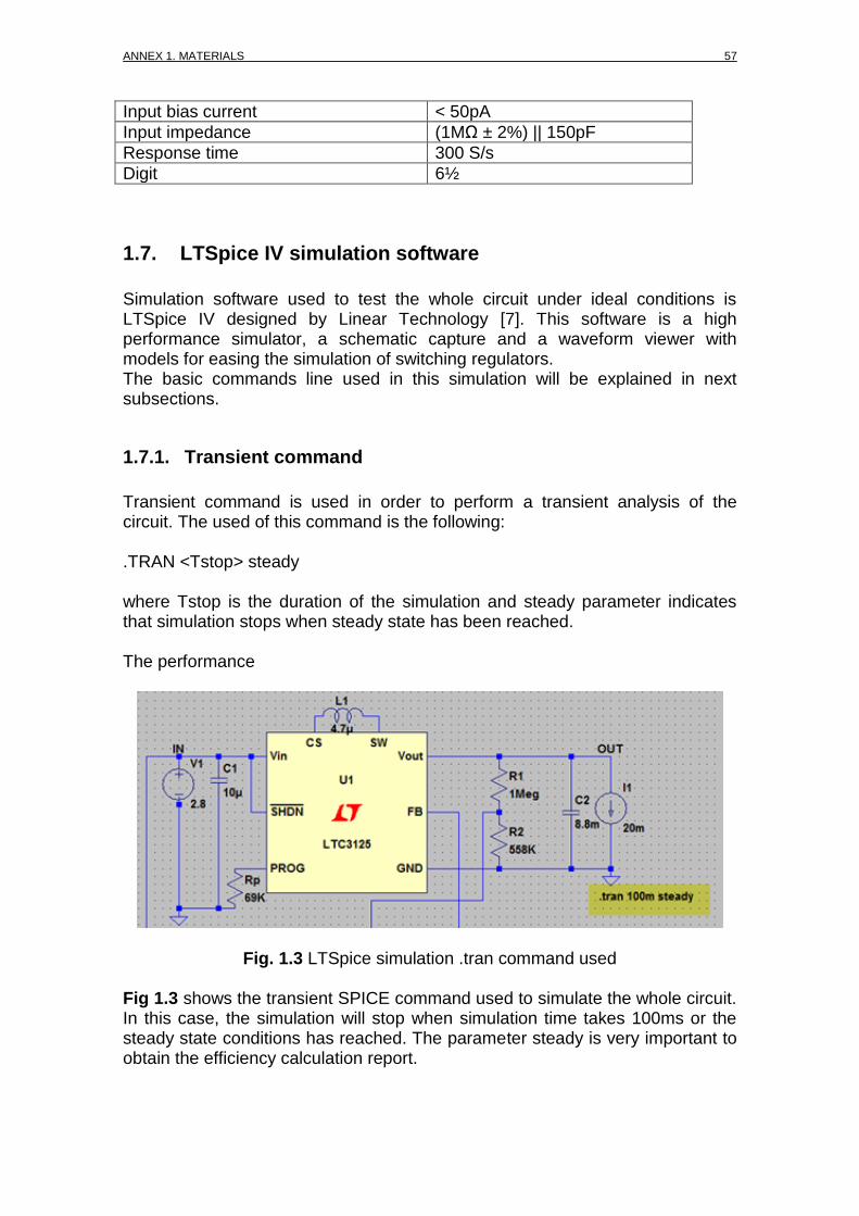
ANNEX 1. MATERIALS 57
Input bias current < 50pA
Input impedance (1MΩ ± 2%) || 150pF
Response time 300 S/s
Digit 6½
1.7. LTSpice IV simulation software
Simulation software used to test the whole circuit under ideal conditions is LTSpice IV designed by Linear Technology [7]. This software is a high performance simulator, a schematic capture and a waveform viewer with models for easing the simulation of switching regulators. The basic commands line used in this simulation will be explained in next subsections.
1.7.1. Transient command
Transient command is used in order to perform a transient analysis of the circuit. The used of this command is the following: .TRAN <Tstop> steady where Tstop is the duration of the simulation and steady parameter indicates that simulation stops when steady state has been reached. The performance
Fig. 1.3 LTSpice simulation .tran command used Fig 1.3 shows the transient SPICE command used to simulate the whole circuit. In this case, the simulation will stop when simulation time takes 100ms or the steady state conditions has reached. The parameter steady is very important to obtain the efficiency calculation report.
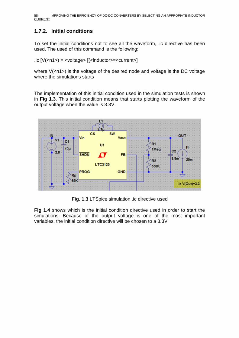
58 IMPROVING THE EFFICIENCY OF DC-DC CONVERTERS BY SELECTING AN APPROPIATE INDUCTOR CURRENT
1.7.2. Initial conditions
To set the initial conditions not to see all the waveform, .ic directive has been used. The used of this command is the following: .ic [V(<n1>) = <voltage> [(<inductor>=<current>] where V(<n1>) is the voltage of the desired node and voltage is the DC voltage where the simulations starts The implementation of this initial condition used in the simulation tests is shown in Fig 1.3. This initial condition means that starts plotting the waveform of the output voltage when the value is 3.3V.
Fig. 1.3 LTSpice simulation .ic directive used Fig 1.4 shows which is the initial condition directive used in order to start the simulations. Because of the output voltage is one of the most important variables, the initial condition directive will be chosen to a 3.3V

ANNEX 2. EFFICIENCY 59
ANNEX 2. EFFICIENCY This annex explains which are the steps to follow to obtain the efficiency in the software simulation.
2.1. Efficiency simulation
To obtain the efficiency simulation of the circuit, we have to do the following steps: a) Simulate the circuit. To do this, go to “Simulate” → “Run” as shown in Fig.
3.17
Fig. 2.1 Simulation of the circuit in LTspice IV software
b) Go the schematic window
c) Right click on schematic window and select “Efficiency Calculation” →
“Mark Start” as shown in Fig. 2.2
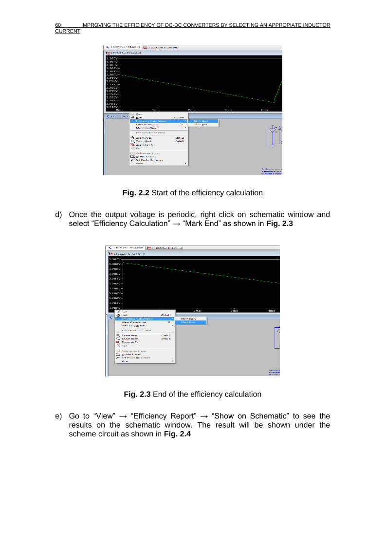
60 IMPROVING THE EFFICIENCY OF DC-DC CONVERTERS BY SELECTING AN APPROPIATE INDUCTOR CURRENT
Fig. 2.2 Start of the efficiency calculation
d) Once the output voltage is periodic, right click on schematic window and
select “Efficiency Calculation” → “Mark End” as shown in Fig. 2.3
Fig. 2.3 End of the efficiency calculation
e) Go to “View” → “Efficiency Report” → “Show on Schematic” to see the
results on the schematic window. The result will be shown under the scheme circuit as shown in Fig. 2.4
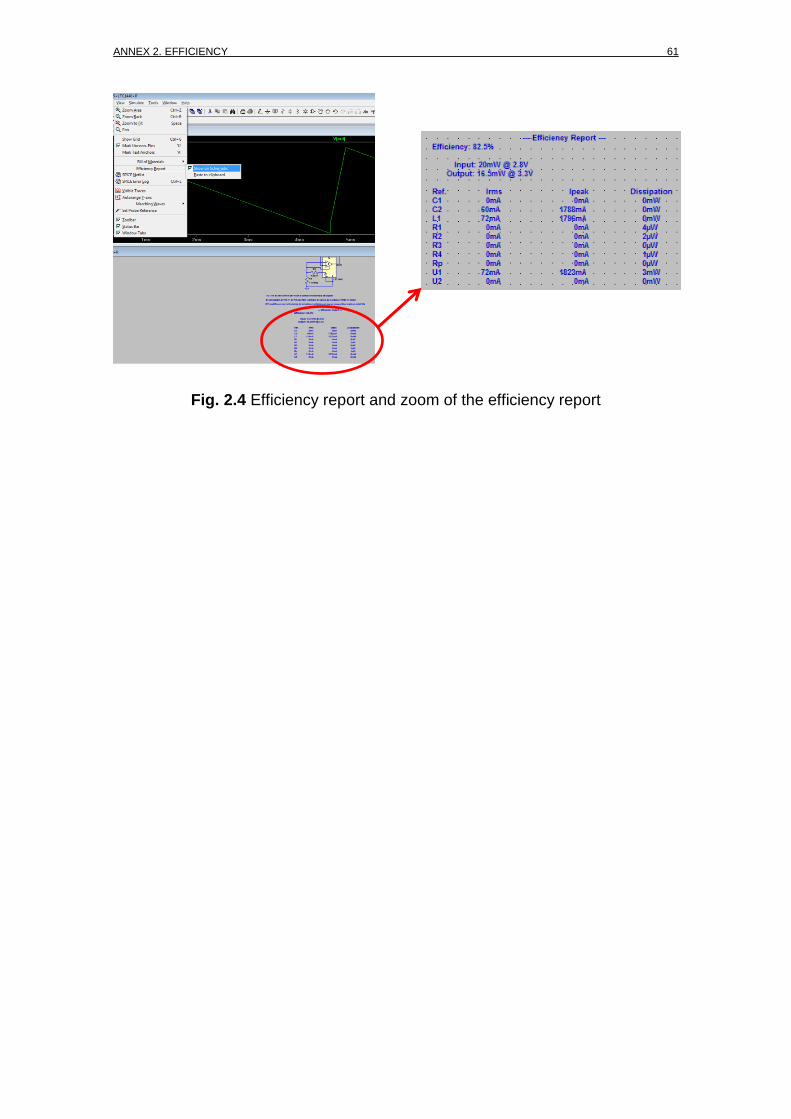
ANNEX 2. EFFICIENCY 61
Fig. 2.4 Efficiency report and zoom of the efficiency report