Embed Size (px)
Citation preview

IEEE TRANSACTIONS ON COMPONENTS, PACKAGE AND MANUFACTURING TECHNOLOGY, 2016
1
Abstract— This paper investigates the performance and
reliability of micro-contacts under low frequency, low amplitude,
alternating current (AC) test conditions. Current micro-contact
theory is based on DC tests adapted to RF applications. To help
better apply DC theory to RF applications, frequencies between 100
Hz to 100 kHz were experimentally investigated. Micro-contacts
designed to conduct performance and reliability measurements
were used, which in prior DC testing typically lasted 100 million
cycles or more. Under AC loads, at similar power levels, eight
devices were tested under cold-switched conditions and only one
was still operational at 10 million cycles. The effect of external
circuitry on DC loaded devices was also considered. Experimental
data was presented for DC conditions which demonstrated that both
a parallel capacitance with a micro-contact as well as a series
inductance were both highly detrimental. For all six tested devices,
failure occurred typically in 100 thousand cycles or less. However,
utilizing series resistive/capacitive circuits as well as parallel
resistor/inductive which resulted in improved performance, with
only one device of the four tested failing prematurely, but those
which lasted showed less variation in measure contact resistance
throughout the lifetime of the device. Two devices were tested with
passive contact protection using parallel and series resistance, and
both devices lasted the full test duration. Finally, the effects of
applying circuit protection to micro-contacts and repeating AC test
conditions was investigated. Reliability and device lifetime was
extended significantly (9.1% success rate without protection was
increased to 87% success rate). It was also observed in several
instances that devices which failed showed subtle signs of variance
during contact closure measurements in the range of 5 to 30 µN,
indicating a possible means for accurately predicting device failure.
For these failed devices, noticeable physical damage was observed
using a scanning electron microscope (SEM).
Index Terms— Contact Resistance, Low-frequency noise,
Microswitches, Microelectromechanical Systems, Prediction
Theory, Reliability, RF Micro-Contacts, Switching Frequency
Submitted 31 January 2016 to IEEE Transactions on Components,
Packaging and Manufacturing Technology (TCPMT). T.V. Laurvick is a PhD candidate with the Air Force Institute of
Technology. Department of Electrical and Computer Engineering, Wright-
Patterson AFB, OH, 45433USA (e-mail: [email protected]). R.A. Coutu, Jr. is an Associate Professor with the Air Force Institute of
Technology. Department of Electrical and Computer Engineering, Wright-
Patterson AFB, OH, 45433USA (e-mail: [email protected]). The views expressed in this article are those of the authors and do not
reflect the official policy or position of the United States Air Force,
Department of Defense, or the U.S. Government.
I. INTRODUCTION
ICRO-switches have been under investigation for years,
and a great deal of research has occurred recently to
address specific concerns in applying these devices to RF
applications [1][2][3]. The many benefits of using these
microelectromechanical (MEMS) devices are apparent, yet
reliability remains an issue [4]. Most of our most current
theory is based on results obtain under DC conditions. Thus,
application of this theory may not directly relate to RF
application. Until performance and reliability are better
understood, mitigation is difficult and until we are able to
apply mitigation, utilization on a large scale will be limited.
To help break this barrier, we need an understanding of how to
apply our DC based predictions, starting with low-frequency
AC applications. Then with this understanding we can better
predict the effects of increased frequency and understand
device breakdown under these conditions. Thus,
investigations such as this are crucial to understanding how
best to mitigate these failures.
At the heart of this study is the observations that the polarity
of a DC load applied to a micro-contact can be critical to its
long-term performance and that material transfer due to
electromigration [5] can be induced under low frequency AC
loads. During closure, asperities due to the roughness of the
surface may induce high current densities [6], which then
promote extremely localized joule heating, which can change
contact geometry [7], increasing contact resistance, which then
promotes more heating [8]. Typically, a combination of these
two effects (high current densities ultimately leading to
electromigration) has been observed repeatedly and attributed
to contact failure. Under any AC conditions, devices are
exposed to a constantly alternating polarity. However, if
polarity is critical to micro-contact reliability, then we are
operating these devices in a manner where favorable and
unfavorable polarity is constantly imposed. Understanding the
effects of this mode of operation, and effective mitigation
techniques for this becomes critical and investigating lower
frequencies helps simplify the task.
Looking to prior efforts in mitigating these device failures,
it has been demonstrated that external circuitry can have a
significant effect under DC conditions [9]. While the
motivation for this protective circuitry has been to address hot-
switching damage, testing the effectiveness of this sort of
protection with low-frequency AC loads is the next task.
Improving Gold/Gold Micro-Contact Performance and
Reliability under Low Frequency AC through Circuit
Loading
Tod V. Laurvick and Ronald A. Coutu, Jr., Senior Member, IEEE
M
IEEE TRANSACTIONS ON COMPONENTS, PACKAGE AND MANUFACTURING TECHNOLOGY, 2016
2
Thus, the goal is to investigate not only how micro-contacts
behave during closure with an AC load, but also the effects of
this polarity reversal during cold-switching in a closed micro-
contact, how is performance and reliability altered under these
conditions, and can these effects be mitigated.
II. TEST SETUP
A. Test Stand
To better control experimental complexity and minimize
the number of variables affecting the results, these
experiments utilized micro-contacts which were designed to
be externally actuated. A test stand designed specifically to
gather data on the contacting surfaces was used under
controlled test conditions. This stand applied a known,
controllable contact force throughout all stages of the
experiment, calculating contact resistance measurements from
currents and voltages measured using an NI-4070
FlexDMM™ module (+/- 110 nΩ of accuracy). Actuation
position was controlled with a ThorLAB™ PAZ005 actuator,
and force was measured using a FemptoTools™ model FT-
5270 sensor. MEMS micro-contacts were fabricated for use
with this test stand, allowing for several controlled tests to be
conducted, each evaluating variables of interest.
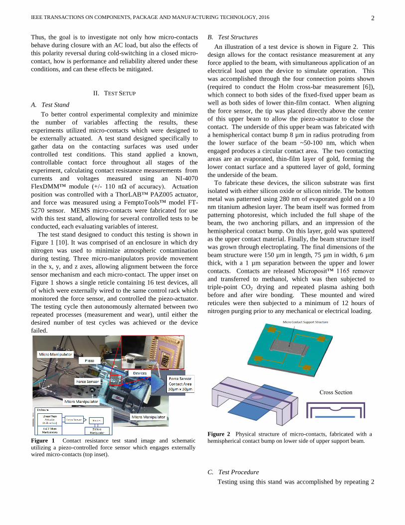
The test stand designed to conduct this testing is shown in
Figure 1 [10]. It was comprised of an enclosure in which dry
nitrogen was used to minimize atmospheric contamination
during testing. Three micro-manipulators provide movement
in the x, y, and z axes, allowing alignment between the force
sensor mechanism and each micro-contact. The upper inset on
Figure 1 shows a single reticle containing 16 test devices, all
of which were externally wired to the same control rack which
monitored the force sensor, and controlled the piezo-actuator.
The testing cycle then autonomously alternated between two
repeated processes (measurement and wear), until either the
desired number of test cycles was achieved or the device
failed.
B. Test Structures
An illustration of a test device is shown in Figure 2. This
design allows for the contact resistance measurement at any
force applied to the beam, with simultaneous application of an
electrical load upon the device to simulate operation. This
was accomplished through the four connection points shown
(required to conduct the Holm cross-bar measurement [6]),
which connect to both sides of the fixed-fixed upper beam as
well as both sides of lower thin-film contact. When aligning
the force sensor, the tip was placed directly above the center
of this upper beam to allow the piezo-actuator to close the
contact. The underside of this upper beam was fabricated with
a hemispherical contact bump 8 µm in radius protruding from
the lower surface of the beam ~50-100 nm, which when
engaged produces a circular contact area. The two contacting
areas are an evaporated, thin-film layer of gold, forming the
lower contact surface and a sputtered layer of gold, forming
the underside of the beam.
To fabricate these devices, the silicon substrate was first
isolated with either silicon oxide or silicon nitride. The bottom
metal was patterned using 280 nm of evaporated gold on a 10
nm titanium adhesion layer. The beam itself was formed from
patterning photoresist, which included the full shape of the
beam, the two anchoring pillars, and an impression of the
hemispherical contact bump. On this layer, gold was sputtered
as the upper contact material. Finally, the beam structure itself
was grown through electroplating. The final dimensions of the
beam structure were 150 µm in length, 75 µm in width, 6 µm
thick, with a 1 µm separation between the upper and lower
contacts. Contacts are released Microposit™ 1165 remover
and transferred to methanol, which was then subjected to
triple-point CO2 drying and repeated plasma ashing both
before and after wire bonding. These mounted and wired
reticules were then subjected to a minimum of 12 hours of
nitrogen purging prior to any mechanical or electrical loading.
C. Test Procedure
Testing using this stand was accomplished by repeating 2
Figure 2 Physical structure of micro-contacts, fabricated with a
hemispherical contact bump on lower side of upper support beam.
Figure 1 Contact resistance test stand image and schematic
utilizing a piezo-controlled force sensor which engages externally
wired micro-contacts (top inset).
IEEE TRANSACTIONS ON COMPONENTS, PACKAGE AND MANUFACTURING TECHNOLOGY, 2016
3
processes in succession: the measurement process and wear
process.
The measurement process was conducted by applying a 1
volt DC load to the beam and slowing advancing the force
sensor in 20 nm increments until contact was made between
the sensor and the beam. The sensor continued to advance
until current was detected through the contact, and a voltage
drop was observed. At this point the force on the sensor
reading was marked, and treated as an offset, effectively
resetting the force measurement to zero. The piezo actuator
continued to advance until the desired contact force was
obtained (200 µN for all results presented here), all while
recording the current through the micro-contact, the voltage
across it, and the force applied to it. A sample of one of these
measurement cycles will be shown in (Figure 12), but the final
resistance which the contact settles to was used as the single
reportable value when plotting contact resistance vs. number
of cycles. Contact resistance was calculated from these
measured values by using the Holm crossbar technique [6].
This technique uses a known current flowing through the
contact while measuring the voltage across the contact, and
from these two values, contact resistance was calculated. As
the voltage measurement was performed with a high
impedance volt meter, this effectively isolated the voltage
measured to the contact itself. This produces a detailed set of
data relating contact resistance to contact force.
The wear process was used to induce wear upon the contact
in the shortest period of time feasible. Knowing the position
required to achieve contact closure from the last measurement
allowed for the piezo-actuator to be positioned and cycled at
high frequencies (up to 2.5 kHz) to impose repeated wear on
the device. At the correct time during contact closure, a load
was applied and then removed to simulate contact operation.
The stand was designed for this load to be a low voltage DC
load but this signal can be used as a waveform trigger to
instead test with an AC load. Failure during this part of the
process results in recording the number of cycles induced up
to that point, along with the failure type (either failure to open
or failure to close). Contact resistance data was not collected
during this process.
The frequency of data collection can be run in two modes.
For testing to a low number of cycles (< ~100,000), data can
be collected repeatedly every certain number of cycles.
However, this becomes impractical for longer tests as the test
measurement process alone can take anywhere between 2 to
10 minutes per data point depending on the device and how it
is set up. For a small number of measurements this is trivial,
but becomes overwhelming at large numbers of cycles. So for
devices tested to higher lifetimes, it becomes necessary to
collect data a set number of times per decade. Note that
measuring a set number of times per decade requires that as
the devices ages, more cycles are imposed between
measurements, which makes short-term changes difficult to
detect. Balancing the desired number of cycles, the number of
devices to be tested, data resolution, and accomplishing this in
the time permitted requires a tradeoff which then must be
accounted for when analyzing the results.
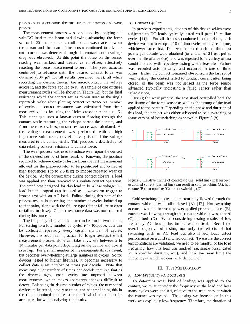
D. Contact Cycling
In previous experiments, devices of this design which were
subjected to DC loads typically lasted well past 10 million
cycles [11]. For all the tests conducted in this effort, each
device was operated up to 10 million cycles or device failure,
whichever came first. Data was collected such that three test
points per decade were obtained (or a total of 21 test points
over the life of a device), and was repeated for a variety of test
conditions and with repetitive testing where feasible. Failure
was recorded automatically, and occurred in one of three
forms. Either the contact remained closed from the last set of
wear testing, the contact failed to conduct current after being
closed, or the beam was not sensed as the force sensor
advanced (typically indicating a failed sensor rather than
failed device).
During the wear process, the test stand controlled both the
oscillation of the force sensor as well as the timing of the load
applied to the contact. Depending on the phase and duration of
this load, the contact was either subjected to cold switching or
some version of hot switching as shown in Figure 3 [9].
Cold switching implies that current only flowed through the
contact while it was fully closed (A) [12]. Hot switching
occurred when either voltage was applied prior to closure (B),
current was flowing through the contact while it was opened
(C), or both (D). When considering testing results of low
frequency AC loads, this timing was critical. Recall the
overall objective of testing not only the effects of hot
switching with an AC load but also if AC loads affect
performance on a cold switched contact. To ensure the correct
test conditions are validated, we need to be mindful of the load
frequency, how this load was applied (i.e. single burst, gated
for a specific duration, etc.), and how this may limit the
frequency at which we can cycle the contact.
III. TEST METHODOLOGY
A. Low Frequency AC Load Tests
To determine what kind of loading was applied to the
contact, we must consider the frequency of the load and how
many cycles were applied, relative to the frequency at which
the contact was cycled. The testing we focused on in this
work was explicitly low-frequency. Therefore, the duration of
Figure 3 Relative timing of contact closure (solid line) with respect
to applied current (dashed line) can result in cold switching (A), hot
closure (B), hot opening (C), or hot switching (D).

IEEE TRANSACTIONS ON COMPONENTS, PACKAGE AND MANUFACTURING TECHNOLOGY, 2016
4
even a single cycle of the load requires the switch be closed
during its duration if we wish to maintain cold-switching
conditions. In order to accommodate this timing requirement,
the frequency at which testing could occur was limited. The
relative timing of these events is shown in Figure 4.
In part (A), a test frequency of 2 kHz was used, which
required a beam actuation signal as shown in relation to a
single cycle of a 10 kHz pulse. As the beam actuation signal
oscillated, contact was made at point (a) in Figure 4, part A.
Contact force continued to increase until point (b) where we
considered the contact fully closed. The exact width of this
region of full closure depends on precisely how far the force
sensor was from the device during test setup, but normally was
controlled to approximately this range of closure. Force
continues to increase and reaches its maximum (200 µN)
when the beam actuation signal peaks, then decreases once
again to point (c). Lightly loaded contact closure occurs
between points (c) and (d), and outside this region, the contact
is open. This means that during full contact closer, the contact
force does vary, however as will be shown in the results
section (Figure 12), a stable contact of this design reaches a
value close to the steady state value at only ~30-50 μN, with
very minimal change in contact resistance beyond this contact
force.
The second condition (B), shows the same two relative
frequencies but with an inverted load. The third case (C),
demonstrates trailing edge hot switching due to a second cycle
imposed on the load and the contact cycling frequency
remains unchanged.
These distinctions were not only relevant because the
contacts were hot or cold switched, but also because they
experienced current flow in both directions while contact
closure occurred. When testing a contact under DC
conditions, it has been demonstrated that two identical
contacts tested in the same manner but with an opposite
polarity on the applied load can drastically affect the longevity
of the contact [10], even if both contact materials are similar
materials, such as gold/gold as relevant properties such as
hardness and elasticity vary depending upon the method of
deposition of the two contacting layers. If we then subject a
contact to hot-switching conditions as in part (C) of Figure 4,
the contact is thus subjected to repeated reverse biasing in
addition to any potential damage caused by hot-switching the
device [8].
This then leads us to consider how to mitigate damage
caused by this manner of operation. To accomplish this, we
investigated external circuit loading effects, and specifically if
certain configurations may aid in prolonging device life [13].
We will start with considering these external circuit loading
effects perform under DC conditions.
B. External Circuit Loading Tests
To investigate this concept, we will build on work
previously published which theorizes on the effects of external
inductance, capacitance, and resistance on micro-contact
behavior [13]. To briefly summarize the theory, potential
damage caused during leading edge hot switching was due to
transient charge on the contacting surface. During contact
closure, this charge leads to regions of extremely high current
density followed by contact closure over the weakened
material. This charge results from the capacitive nature of a
pair of contacts prior to closure, and any external capacitance
in parallel with such a contact can in theory amplify the effect
[13].
Similarly, during trailing edge hot switching, this theory
predicts that damage results from the transient current flowing
through a contact which attempts to continue to flow after the
contact begins to open, which can similarly lead to regions of
extremely high current density. In this case, any external
series inductance can similarly exaggerate these kinds of
effects.
This work also postulates that these effects may be
mitigated by applying these active components in the opposite
manner (i.e. parallel inductance to mitigate pre-closure surface
charge, series capacitance to mitigate maintained current
flow), or even if the addition of passive components could
produce a similar effect by applying voltage and current
limiting elements during operation.
To experimentally validate this theory, testing was
Figure 4 Timing of test signals relative to beam actuation signal (voltage vs.
msec). In case A, a single cold-switched cycle was induced, starting with
unfavorable polarity for half the cycle and favorable for the second half, where load was applied within window of contact closure (between (b) and
(c)). Point (a) represented where the contact gap closed and contact was
made, but at zero contact force, and between (c) and (d) the contact was opening. Outside these regions, the contact was opened fully. Part B is the
‘inverted’ signal, and C was an extended signal which intentionally induce
AC hot switching conditions.
IEEE TRANSACTIONS ON COMPONENTS, PACKAGE AND MANUFACTURING TECHNOLOGY, 2016
5
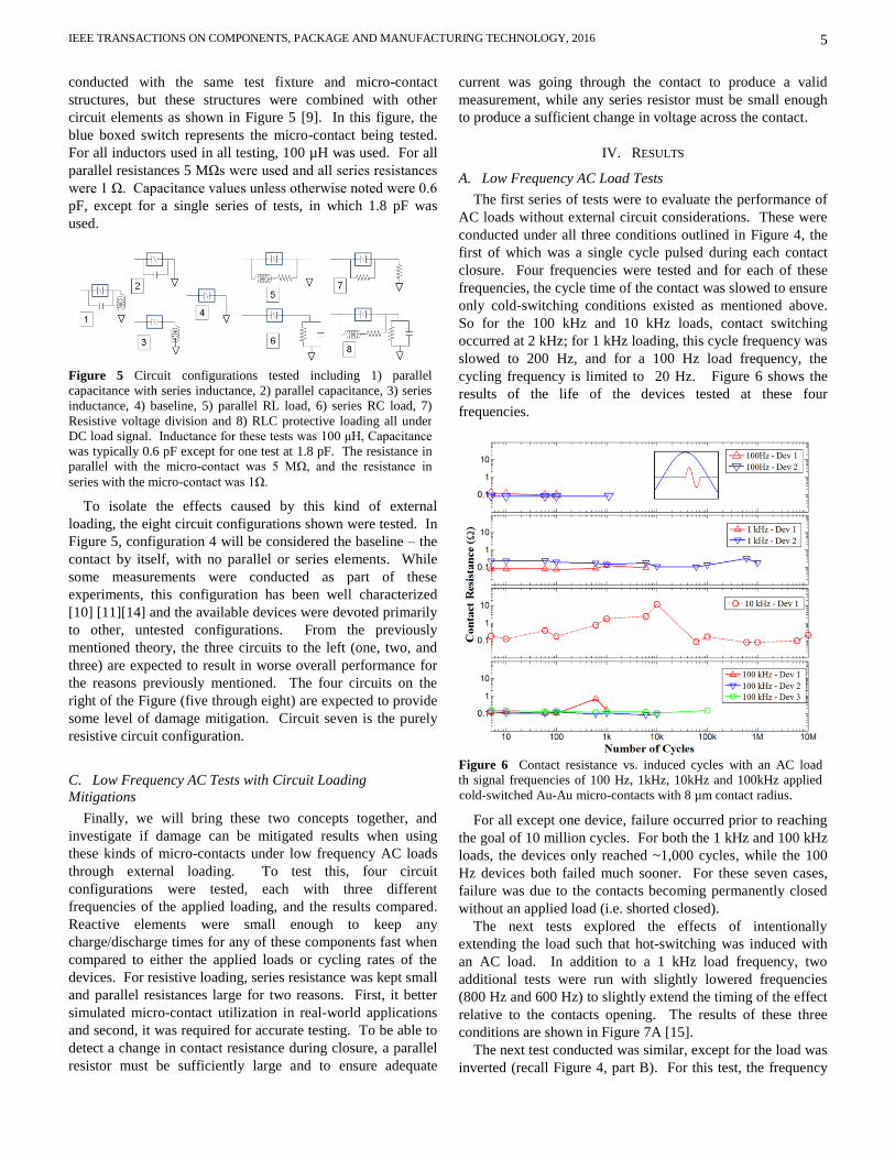
conducted with the same test fixture and micro-contact
structures, but these structures were combined with other
circuit elements as shown in Figure 5 [9]. In this figure, the
blue boxed switch represents the micro-contact being tested.
For all inductors used in all testing, 100 µH was used. For all
parallel resistances 5 MΩs were used and all series resistances
were 1 Ω. Capacitance values unless otherwise noted were 0.6
pF, except for a single series of tests, in which 1.8 pF was
used.
To isolate the effects caused by this kind of external
loading, the eight circuit configurations shown were tested. In
Figure 5, configuration 4 will be considered the baseline – the
contact by itself, with no parallel or series elements. While
some measurements were conducted as part of these
experiments, this configuration has been well characterized
[10] [11][14] and the available devices were devoted primarily
to other, untested configurations. From the previously
mentioned theory, the three circuits to the left (one, two, and
three) are expected to result in worse overall performance for
the reasons previously mentioned. The four circuits on the
right of the Figure (five through eight) are expected to provide
some level of damage mitigation. Circuit seven is the purely
resistive circuit configuration.
C. Low Frequency AC Tests with Circuit Loading
Mitigations
Finally, we will bring these two concepts together, and
investigate if damage can be mitigated results when using
these kinds of micro-contacts under low frequency AC loads
through external loading. To test this, four circuit
configurations were tested, each with three different
frequencies of the applied loading, and the results compared.
Reactive elements were small enough to keep any
charge/discharge times for any of these components fast when
compared to either the applied loads or cycling rates of the
devices. For resistive loading, series resistance was kept small
and parallel resistances large for two reasons. First, it better
simulated micro-contact utilization in real-world applications
and second, it was required for accurate testing. To be able to
detect a change in contact resistance during closure, a parallel
resistor must be sufficiently large and to ensure adequate
current was going through the contact to produce a valid
measurement, while any series resistor must be small enough
to produce a sufficient change in voltage across the contact.
IV. RESULTS
A. Low Frequency AC Load Tests
The first series of tests were to evaluate the performance of
AC loads without external circuit considerations. These were
conducted under all three conditions outlined in Figure 4, the
first of which was a single cycle pulsed during each contact
closure. Four frequencies were tested and for each of these
frequencies, the cycle time of the contact was slowed to ensure
only cold-switching conditions existed as mentioned above.
So for the 100 kHz and 10 kHz loads, contact switching
occurred at 2 kHz; for 1 kHz loading, this cycle frequency was
slowed to 200 Hz, and for a 100 Hz load frequency, the
cycling frequency is limited to 20 Hz. Figure 6 shows the
results of the life of the devices tested at these four
frequencies.
For all except one device, failure occurred prior to reaching
the goal of 10 million cycles. For both the 1 kHz and 100 kHz
loads, the devices only reached ~1,000 cycles, while the 100
Hz devices both failed much sooner. For these seven cases,
failure was due to the contacts becoming permanently closed
without an applied load (i.e. shorted closed).
The next tests explored the effects of intentionally
extending the load such that hot-switching was induced with
an AC load. In addition to a 1 kHz load frequency, two
additional tests were run with slightly lowered frequencies
(800 Hz and 600 Hz) to slightly extend the timing of the effect
relative to the contacts opening. The results of these three
conditions are shown in Figure 7A [15].
The next test conducted was similar, except for the load was
inverted (recall Figure 4, part B). For this test, the frequency
Figure 6 Contact resistance vs. induced cycles with an AC load
with signal frequencies of 100 Hz, 1kHz, 10kHz and 100kHz applied
to cold-switched Au-Au micro-contacts with 8 µm contact radius.
Figure 5 Circuit configurations tested including 1) parallel
capacitance with series inductance, 2) parallel capacitance, 3) series
inductance, 4) baseline, 5) parallel RL load, 6) series RC load, 7)
Resistive voltage division and 8) RLC protective loading all under
DC load signal. Inductance for these tests was 100 μH, Capacitance
was typically 0.6 pF except for one test at 1.8 pF. The resistance in
parallel with the micro-contact was 5 MΩ, and the resistance in
series with the micro-contact was 1Ω.

IEEE TRANSACTIONS ON COMPONENTS, PACKAGE AND MANUFACTURING TECHNOLOGY, 2016
6
selected was 10 kHz, which provided the best results in the
first set of testing. Figure 7B [15] shows both the non-
inverted results from the first test along with the results of the
inverted test. This device also lasted to 10 million cycles and
showed little difference when compared to the non-inverted
tests.
If we bend back the upper beams for some of these failed
devices, we can investigate the damaged surfaces with an
SEM, as shown in Figure 8 [15].
The left side of each pair of images shows the
hemispherical bump discussed previously, and the profile of
this feature becomes apparent in the shadowing of the surface.
The right images show the corresponding lower contact
surfaces. The top two images are from the 100 kHz device
from the first test series and the second two images from the
10 kHz device from same tests. The bottom two images are
from a previous device subjected to DC testing [10]. This
unloaded DC device showed stable performance up to 10
million cycles, at which point testing was halted so the device
could be examined to look for any signs of wear. Note that
the failed devices (in some cases with only a few thousand
cycles), showed significant damage due to material being
transferred between contacts, with pits where material was
removed and the debris produced in some cases still evident.
In both cases, the contact location on the lower surface (which
was the center of the patterned circle) shows very little signs
of wear, indicating the damage was inflicted primarily to the
sputtered upper contact and not the evaporated lower contact.
B. External Circuit Loading Tests
To discuss the results of external loading on micro-contact
performance, recall the eight circuits presented in Figure 5.
These circuits were ordered by expected performance, where
circuit configurations one, two, and three incorporated all the
elements which were expected to be detrimental. Circuit four
was the baseline with no external elements. Configurations
five, six, and eight included reactive elements in what was
theorized as beneficial configurations, and circuit
configuration seven was purely resistive. A single baseline
was run (circuit four) to ensure performance was comparable
to results from previous studies conducted with this design. In
~40 devices previously tested under identical baseline
conditions, typical contact resistance between ~0.1 Ωs to ~2
Ωs was common, with greater variance under 1,000 cycles
occasionally occurring as the device was worn in [10]
[11][14]. For the other seven circuits, two devices were tested
with each setup.
First, consider the three detrimental circuit configurations
(one, two, and three). The worst of these three circuits was the
circuit which contained an inductor in series with the micro-
contact. While the other two configurations all failed well
short of the 10 million cycle goal, series inductance failed
much sooner. Figure 9 [9] shows a comparison of the two
devices tested in this configuration with a 1 VDC load,
compared to the baseline device (circuit configuration 4),
which lasted to 10 million cycles and was still functional at the
point of test termination.
Figure 8 Exposed contacts after folding back the upper beams (left)
and their corresponding lower pads (right) from three devices
exposed to cold switched loads, at 100 kHz, 10 kHz AC loads (as
labeled), compared to identical device tested with cold switched DC
to 10M cycles of operation. The circular shape on the pad side is an
intentional conformal feature in the bottom evaporated gold layer
which marks the corresponding outer radius of the mating bump (in
which the same circular shape can be seen, but is diminished during
the photoresist reflow process which gives the upper beam contacts
a hemispherical shape.
Figure 7 (A) Comparison of hot-switched, AC loads of frequencies
1 kHz, 800 Hz, and 600 Hz where all three devices eventually failed
to open. (B) Comparison of cold-switched loading of inverted and
non-inverted single cycle, 10 kHz loads applied to 8 µm contact
radius Au-Au micro-contact cycled at 2 kHz.

IEEE TRANSACTIONS ON COMPONENTS, PACKAGE AND MANUFACTURING TECHNOLOGY, 2016
7
Next, consider the three reactive, damage mitigating circuits
from Figure 5 (configurations five, six, and eight). For all
three of these tests, all devices tested lasted to the 10 million
cycle goal and were still functional upon test termination. The
configuration in which both devices appears to be the most
stable was the series RC configuration (Figure 5, circuit six).
The comparison of the two devices tested in this configuration
along with the same unloaded element as shown previously,
are shown in Figure 10 [9].
While some variance was still present in the contact
resistance, the reactive element circuit devices all recovered
from any of these fluctuations and were able to ‘dial in’ to a
final contact resistance very effectively. Next, consider the
purely resistive configuration as shown in Figure 11 [9].
Recall from section II, part C where the measurement
process was described for these devices. As the force sensor
assembly was advanced and applied an ever increasing
external force to the upper beam of the contact support
structure, contact resistance was measured at each step
providing a detailed profile of contact resistance vs. contact
force. If we look closely at data collected from a device which
failed prematurely, we observed the last few measurements
taken showed signs of the impending failure. To illustrate
this, consider Figure 12 [9].
The two curves in this plot show data from two different
devices, one which lasted to 10M cycles without incident
(‘Stable Contact’ in Figure 12) and one which failed before
that point (‘Failing Contact’ in Figure 12). This particular
measurement is from the device shown in Figure 9(B), device
(b) - parallel capacitance. This is the data from the
measurement taken at ~1,000 cycles (two measurements
before failing at ~10,000 cycles), which is when this abnormal
curve first appeared. The second device shown in Figure 12,
labeled ‘stable contact’ was the last test measurement from a
device that had reached 10 million cycles and was still
operational. The variation between the smooth, exponential
Figure 9 Comparison of the contact resistance of Au-Au 8μm
radius micro-contacts to three detrimental circuits. Series inductance
of 100 µH was added for (A), parallel capacitance of 0.6 pF was
added for (B), and both elements were added to (C). All six devices
were tested with a 1 volt, cold-switched DC load, and all failed due
to shorting at the number of cycles shown.
Figure 11 Comparison of the contact resistance of Au-Au 8μm
radius micro-contacts showing an unloaded device along with both a
5 MΩ parallel resistance, capable of immediately dissipating any
charge during contact opening, and a series resistance of 1 Ω,
providing the ability to limit current while contact was closed.
Figure 10 Comparison of the contact resistance of unloaded Au-
Au 8μm radius micro-contacts with two protective circuits. The
first (A) shows two series RC external loads (a) and (b), the second
(B) shows both series RC and parallel RL. The one failed device
was due to shorting, the rest all lasted to the target 10M cycles.
The external resistor used was 1 Ω , the capacitor was 0.6 pF and
inductor was 100 µH.
Figure 12 Comparison of two single contact resistance
measurements cycles, one at 10 million cycles for a device that
remained stable, the second shows a measurement shortly before
the device failed, where it no longer conducted current upon
closing.

IEEE TRANSACTIONS ON COMPONENTS, PACKAGE AND MANUFACTURING TECHNOLOGY, 2016
8
decay of the stable device vs. the irregularity in the failing
device may prove to be a viable method to monitor the
“health” of these devices during operation.
As in the last set of experiments, one of the contacts was
imaged using SEM imagery. The device selected had purely
resistive protection and was investigated after it appeared to
recover and settle (device (a) shown in Figure 11). The SEM
results are shown in Figure 13 [9]. In the larger image on the
bottom, an expanded view is provided of a beam folded back
with a probe, and on the top are close-up views of both sides
of the micro-contact. This was the same method which was
used to image the contacts shown in Figure 8. While there
was signs of transferred material, note that this material does
not have the same jagged appearance as the failed devices
from Figure 8. While there was one small spot of material on
the bottom of the contact bump, overall this image shows little
signs of damage.
C. Low Frequency AC Tests with Circuit Loading
Mitigations
Finally, we investigated the effects of combining this idea
of protecting a circuit through external loading, and test
devices with these external circuits while exposing them to the
same AC loads as we used earlier and see if we can get
improved results.
For this series of tests, we used three frequency loads - 1
kHz, 10 kHz, and 100 kHz. For each, the cycle rate during
testing was adjusted to ensure only cold cycling conditions
applied. For each of these three frequencies, devices were
tested with each of the 4 protective circuit configurations
shown in Figure 5, parts 5-8, and additionally for the series
capacitance circuit configuration, two different capacitances
were investigated for a total of 15 tests conducted.
Of the 15 tests ran, 13 devices ran to 10 million cycles and
were still operation. The first failed test was the 1 kHz load
using parallel inductance which failed at just over 8,000
cycles. The second premature failure was also with a 1 kHz
load but with both series capacitance and parallel inductance
and failed at 4.88 million cycles. All three of these failures
were due to contact shorting during the wear cycling. All
other tests showed very little variation in contact resistance
early in testing, until just after 100,000 cycles. At that point,
in almost every case the contact resistance began to climb with
device life. The results from the purely resistive test are
shown in Figure 14.
The next two tests involved the addition of parallel resistive
loading along with series capacitance. Both tests used 5 MΩ
parallel resistance and a 1 Ω series resistance, but with two
different capacitances (0.6 pF and 1.8 pF). The results are
shown in Figure 15.
Finally, reactive protection was tested which not only
Figure 15 Comparison of contact resistance vs. device life of Au-
Au 8μm radius micro-contacts for two test circuits (both with a 5
MΩ parallel resistance, and an RC circuit in series, using a 1 Ω
series resistance, and along with two different sized capacitances as
shown). The tests were conducted at the three frequencies listed, all
of which were still operational at the 10 million cycle target.
Figure 14 Comparison of contact resistance vs. device life of Au-
Au 8μm radius micro-contacts under the three AC loads shown, all
cold switched with a parallel 5 MΩ resistor and 1 Ω series resistance
added external. All three devices remained operational at the 10
million cycles target.
Figure 13 SEM investigation of contact surfaces after testing to
10M cycles with a DC, cold-switched load to investigate level of
induced wear by folding upper contact beam back after separating
from anchor. This device was tested with passive external circuit
loading, with a 50 MΩ parallel resistance and 1 Ω series resistance.

IEEE TRANSACTIONS ON COMPONENTS, PACKAGE AND MANUFACTURING TECHNOLOGY, 2016
9
utilized series capacitance, but also parallel inductance. The
same resistances were used as in the last two tests, the series
capacitor was 0.6 pF and the parallel inductance was 100 µH.
The results of these tests are shown in Figure 16.
V. CONCLUSIONS
From these results several conclusions can be drawn by
stepping through the experiments performed, considering the
incremental changes applied between tests, and evaluating the
results of these changes.
First consider the history of performance of these devices
under DC loads, with no external loading. While a few
representative devices were tested with each test series
presented here, if we look at data collected over the past
several years, in ~40 devices previously tested under identical
baseline conditions, typical contact resistance between ~0.1
Ωs to ~2 Ωs was common, with greater variance under 1,000
cycles occurring as the device were worn in. Of these 40
devices, the failure rate prior to 20 million cycles was ~5%.
This data was taken with devices fabricated at the same time
(and in some cases, on the same wafer) as the data collected
here, so based on this performance record, it was assumed that
if there was significant premature failure it was due to test
conditions imposed and not inherent in the devices
themselves.
Next, consider the results of replacing the DC load with
AC. Due to the limited number of tests for frequency
inversion and hot switching, it would be unreliable to draw too
many correlations to specific frequencies, but overall for all
three devices tested under hot switching conditions, all three
failed prior to the 10 million cycle target. Under cold
switched conditions however, of the eight devices tested, only
one survived to the 10 million cycle point which overall was
an 87.5% failure rate. SEM imagery confirmed that
comparing devices which failed under these AC loads showed
substantial damage when compared to identical contacts
exposed to 10 million cycles of DC loading and were still
operable.
Following this was the investigation of the effects of
external circuits on micro-contact performance, under DC
loading conditions. Theory predicted that series inductance
and parallel capacitance can accelerate premature failure in
micro-contacts, which was validated in all 6 of the test devices
which failed prematurely in these destructive circuit
configurations. Conversely, it was expected that while series
capacitance, and parallel inductance should aid in device
performance. Three of the four devices tested under these
conditions lasted the full test duration. Additionally, passive
protection also behaved as expected and both devices tested
again lasted the full 10 million cycles.
This culminated into the investigation of mitigating the
failure rate of AC load tests by applying external protective
circuit elements. Under test conditions which were identical
to those used in the initial AC testing, of the 12 devices tested,
only one failed. In other words, applying external circuit
protection reduced the failure rate from 87.5% to 8.3%. As
before, drawing specific conclusions on which configurations
performed better than others may not be substantiated given
the limited number of tests for each circuit, but when the
entire data set was considered, these more general
observations are apparent.
One side observation when investigating the detailed data
collected during a single contact resistance measurement, the
'smoothness' of the resistance-force curve produced a
distinctive behavior in devices which failed shortly after
producing these abnormal measurements. By evaluating a
deviation from the idea, smooth curve which contact
resistance theory predicts, one indicator of premature contact
failure becomes available.
REFERENCES
[1] V. S. Cortes and G. Fischer, “Shunt MEMS Switch Requirements
for Tunable Matching Network at 1 . 9 GHz in Composite
Substrates,” GeMiC, vol. March 16–1, pp. 422–425, 2015. [2] A. K. Chaurasia and R. Mehra, “Robust Design of RF MEMS
Switch Design with Reduced Buckeling Effect,” Int. J. Comput.
Appl., vol. 119, no. 24, 2015. [3] V. Mulloni, B. Margesin, F. B. Kessler, R. Marcelli, G. De Angelis,
C. Roma, and P. Farinelli, “Cycling reliability of RF-MEMS
switches with Gold-Platinum multilayers as contact material,” in Symposium on Design Test Integration and packaging of MEMS
and MOEMS, 2015.
[4] G. M. Rebeiz, C. D. Patel, S. K. Han, C. H. Ko, and K. Ho, “The search for a reliable MEMS switch?: Metal-contact switches,” IEEE
Microw. Mag., vol. 14, no. 1, pp. 57–67, 2013.
[5] A. Basu, R. P. Hennessy, G. G. Adams, and N. E. McGruer, “Hot switching damage mechanisms in MEMS contacts—evidence and
understanding,” J. Micromechanics Microengineering, vol. 24, no. 10, pp. 1–16, 2014.
[6] R. Holm, “Electric Contacts,” Springer-Verlag
Berlin/Heidelberg/New York, pp. 1–55,367–397, 1967. [7] M. Braunovic, N. K. Myshkin, and V. V Konchits, Electrical
contacts: fundamentals, applications and technology. CRC press,
2006. [8] Z. Yang, D. Lichtenwalner, a Morris, J. Krim, and a I. Kingon,
“Contact degradation in hot/cold operation of direct contact micro-
switches,” J. Micromechanics Microengineering, vol. 20, p. 105028, 2010.
[9] T. V. Laurvick and R. A. Coutu, “Experimental validation of
external load effects on micro-contact performance and reliability,” 2015 IEEE 61st Holm Conf. Electr. Contacts, pp. 353–357, 2015.
[10] C. Stilson and R. Coutu, “Reliability Evolution of Au-Au, Au-Ru
Figure 16 Comparison of contact resistance vs. device life of Au-
Au 8μm radius micro-contacts for the test circuit shown. The
inductance used was 100 µH along with a 5 MΩ parallel resistance,
as well as an RC circuit in series, using a 1 Ω series resistance, and
0.6 pF of capacitance). The tests were conducted at the three
frequencies listed, two of which were still operational at the 10
million cycle target and one which failed to close just prior to
reaching 10 million cycles.

IEEE TRANSACTIONS ON COMPONENTS, PACKAGE AND MANUFACTURING TECHNOLOGY, 2016
10
and Au-RuO2 Micro-Contacts,” in Proceedings of the 27th
International Conference on Electrical Contacts; ICEC 2014, 2014, pp. 1–6.
[11] C. Stilson and R. Coutu Jr, “Contact resistance evolution of highly
cycled, lightly loaded micro-contacts,” in Reliability, Packaging, Testing, and Characterization of MOEMS/MEMS, Nanodevices, and
Nanomaterials XIII, February 3, 2014 - February 4, 2014, 2014,
vol. 8975, p. Samsung Advanced Institute of Technology; The Soci. [12] G. M. Rebeiz, RF MEMS: Theory, Design, and Technology. 2003.
[13] B. F. Toler and R. A. Coutu Jr., “Characterizing external resistive,
inductive and capacitive loads for micro-switches,” MEMS Nanotechnology, Vol. 6 Proc. 2012 Annu. Conf. Exp. Appl. Mech.,
vol. Costa Mesa, pp. 11–18, 2013.
[14] T. Laurvick, C. Stilson, and R. A. Coutu Jr., “Experimental investigation of thin film spreading resistance in micro-contacts,”
Electr. Contacts (Holm), 2014 IEEE 60th Holm Conf., pp. 1–6,
2014. [15] T. V. Laurvick and R. A. Coutu, “Micro-contact performance and
reliability under low frequency, low amplitude, alternating current
(AC) test conditions,” 2015 IEEE 61st Holm Conf. Electr. Contacts, pp. 222–226, 2015.
Tod V. Laurvick is a PhD student at the Air
Force Institute of Technology (AFIT). He
received his B.S. in electrical engineering
from Michigan Technological University
(MTU) in 1995 and his M.S. in electrical
engineering from AFIT in 2009. During his
time with the Air Force, he has worked as a
flight test engineer for the Airborne Laser
Program as well as a program manager for
the sodium guidestar program (NGAS) at
Starfire Optical Range (SOR). Prior to
receiving his commission, he has over eight
years of industry experience in research and development,
manufacturing, and optimization of factory automation for multiple
industries. He is a member SPIE, Tau Beta Pi and Eta Kappa Nu.
His current research interests are microelectromechanical systems
(MEMS), specifically applied to micro-electrical contact
characterization and optimization, and MEMS energy distribution
and storage. He is also interested advanced fabrication techniques
applications such as atomic layer deposition (ALD) and nano-scale
patterning techniques.
Ronald A. Coutu, Jr. is a Professor of
Electrical Engineering and V. Clayton
Lafferty Endowed Chair in Micro-Sensors
and Smart Sensors at Marquette University,
Milwaukee, WI. He received his B.S. in
electrical engineering from the University of
Massachusetts at Amherst in 1993, his M.S.
in electrical engineering from the California
Polytechnic State University (CalPoly) in
San Luis Obispo in 1995 and his Ph.D. in
electrical engineering from the Air Force
Institute of Technology (AFIT) in 2004. In
2009, he retired from active duty Air Force after serving honorably
for 25 years. He is a California registered Professional Engineer in
electrical engineering and a Senior Member of the IEEE and SPIE.
He is also a Life Member of Tau Beta Pi and Eta Kappa Nu. His
current research interests include microelectromechanical systems
(MEMS), smart sensors, device fabrication, micro-electrical contacts
and phase-change materials. He is also very interested in energy
harvesting, renewable energy, micro-grids and energy storage.


![Improving the process performance of gold cyanide leaching ... · Improving the process performance of gold cyanide leaching reactors 3 literature (Equation [1]) shows that k L a](https://img.pdfslide.us/doc/110x75/5ad34b757f8b9abd6c8dbd36/improving-the-process-performance-of-gold-cyanide-leaching-the-process-performance.jpg)