Embed Size (px)
Citation preview
8/12/2019 Improvement o Fpf
http://slidepdf.com/reader/full/improvement-o-fpf 1/6
2011 IEEE PES Innovative Smart Grid Technologies – India
Abstract —Power electronics systems are non-linear systems,
which consume more reactive power and also the loads they feed
are mostly inductive loads which leads to a poor power factor.
Various compensation techniques are available to bring the
power factor nearer to unity. In this paper, a novel compensator
is proposed, where in-phase and quadrature components of the
supply current are vector-controlled. Implementation of this
compensator in a power electronic system operating with a very
poor power factor (and hence high THD), shows that the systemthen draws a leading current. A conventional power electronic
system with one of the traditional static VAR compensators and
the conventional power electronic system incorporated with the
proposed compensator are simulated and the simulation results
are obtained. It is shown that the proposed method offers only
0.7% THD, which also implies that the power factor is improved.
Index Terms —Total Harmonic Distortion, Vector Control,
Compensator, Switching, Power Electronic Converters
I. I NTRODUCTION
HE Power Electronics converters have been increasingly
employed in recent years owing to their advanced featuresincluding sinusoidal input current at unity power factor. Power
electronic devices that have rapid and frequent load variations
have become abundant today due to their many process
control Supply side is developed. The in-phase component of
the supply current IP is kept constant, whereas the quadrature
component of the supply current IQ is controlled from the
output of the speed loop. The vector control is formulated in
d-q axis coordinated frame, the method requires on-line
coordinate transformations that convert the line current in
three related and energy saving benefits. These features are
not necessarily achieved under the operating conditions of
unbalanced input supply and input impedances. Such a
N. Venkateswarlu is with the Electrical and Electronics Engineering
Department, Audisankara College of Engineering and Technology, Nellore,A.P,INDIA-524101 phone: 0-8624-221942; fax: 0-8624-221942; (e-mail:
venki280@ gmail.com).
M. Vel Murugan is with the Electrical and Electronics EngineeringDepartment, Audisankara College of Engineering and Technology, Nellore,
A.P,INDIA-524101; (e-mail: [email protected]).
J. Suresh is with with the Electrical and Electronics Engineering
Department, Audisankara College of Engineering and Technology, Nellore,
A.P,INDIA-524101; (e-mail: jntu703@ gmail.com).
978-1-4673-0315-6/11/$26.00©2011 IEEE
generalized unbalanced operating condition is quite common
in power systems, as the electrical energy is generated,
transmitted in the form of alternating current. To meet this
requirement, it is customary to add a power factor correction
circuit. The low power factor is due to the power loads that are
inductive which take lagging currents and hence lagging
power factor [4]. To improve the power factor, device
supplying reactive power are connected in parallel to thesystem at desired location. The capacitor draws a leading
current and neutralizes the lagging reactive component of load
current. This raises the power factor of the load. However they
do not regulate the instantaneous power explicitly. So that it is
not suitable for implementation. Various methods of VAR
compensation are synchronous condensers, mechanically
switched capacitors etc.,[7,8].With the advent of power
electronic switches, TSC-Thyristor switched capacitor, has
been used to absorb or inject reactive power[5,6].
This paper proposes a new control scheme in which a vector
control method on the phase rotating frame to two phase
synchronously rotating frame representation and vice versa
[2], [3]. The d-q components of the input voltages and currents
are employed to accurately describe the behavior of the
converter. The proposed vector control scheme [1] allows the
system to draw a leading current. Because the current is
leading, THD is drastically reduced.
Because of the growing concern about harmonic pollution
there is a need to reduce the harmonic contents of the AC line
current of power supplies. Harmonics may disrupt normal
operation of devices. Therefore rapid reactive power changes
demand timely reactive VAR compensation. Even with that,
the THD is not up to the specified standards.
II. CONVENTIONAL METHOD
Fig. 1. A Power Electronics System with No Compensation Technique.
Improvement of Power Factor in Power
Electronic Systems by using a Method of
compensation
N. Venkateswarlu, M. Velmurugan, and J. Suresh
T
8/12/2019 Improvement o Fpf
http://slidepdf.com/reader/full/improvement-o-fpf 2/6
2011 IEEE PES Innovative Smart Grid Technologies – India
A power electronics system with no compensator is shown
in fig 1.
The three phase supply is fed to the three phase rectifier
which further, through a DC link feeds a three phase inverter.
The load used is inductive or non-linear which will draw
lagging current and hence poor power factor results.
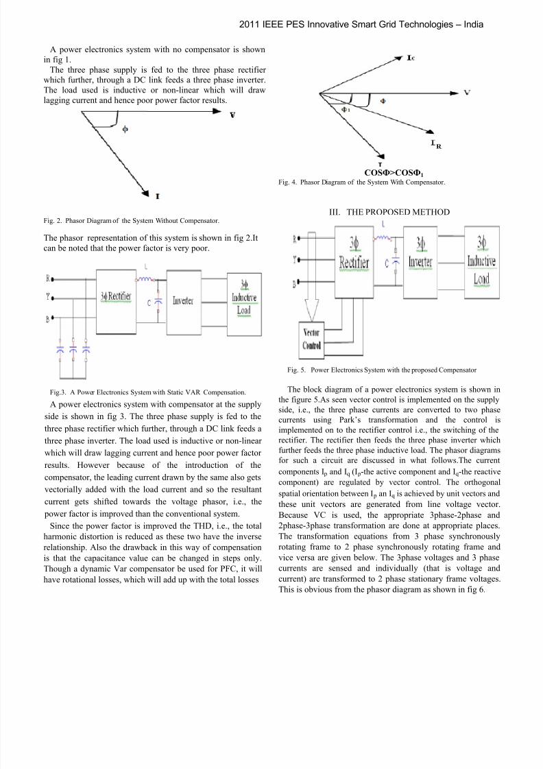
Fig. 2. Phasor Diagram of the System Without Compensator.
The phasor representation of this system is shown in fig 2.It
can be noted that the power factor is very poor.
Fig.3. A Power Electronics System with Static VAR Compensation.
A power electronics system with compensator at the supplyside is shown in fig 3. The three phase supply is fed to the
three phase rectifier which further, through a DC link feeds a
three phase inverter. The load used is inductive or non-linear
which will draw lagging current and hence poor power factor
results. However because of the introduction of the
compensator, the leading current drawn by the same also gets
vectorially added with the load current and so the resultant
current gets shifted towards the voltage phasor, i.e., the
power factor is improved than the conventional system.
Since the power factor is improved the THD, i.e., the total
harmonic distortion is reduced as these two have the inverserelationship. Also the drawback in this way of compensation
is that the capacitance value can be changed in steps only.
Though a dynamic Var compensator be used for PFC, it will
have rotational losses, which will add up with the total losses
COSФ>COSФ1 Fig. 4. Phasor Diagram of the System With Compensator.
III. THE PROPOSED METHOD
Fig. 5. Power Electronics System with the proposed Compensator
The block diagram of a power electronics system is shown in
the figure 5.As seen vector control is implemented on the supply
side, i.e., the three phase currents are converted to two phase
currents using Park’s transformation and the control is
implemented on to the rectifier control i.e., the switching of the
rectifier. The rectifier then feeds the three phase inverter which
further feeds the three phase inductive load. The phasor diagrams
for such a circuit are discussed in what follows.The current
components I p and Iq (I p-the active component and Iq-the reactive
component) are regulated by vector control. The orthogonal
spatial orientation between I p an Iq is achieved by unit vectors and
these unit vectors are generated from line voltage vector.
Because VC is used, the appropriate 3phase-2phase and
2phase-3phase transformation are done at appropriate places.
The transformation equations from 3 phase synchronouslyrotating frame to 2 phase synchronously rotating frame and
vice versa are given below. The 3phase voltages and 3 phase
currents are sensed and individually (that is voltage and
current) are transformed to 2 phase stationary frame voltages.
This is obvious from the phasor diagram as shown in fig 6.
8/12/2019 Improvement o Fpf
http://slidepdf.com/reader/full/improvement-o-fpf 3/6
Fig .6. Phasor diagram of the proposed sch
implementation
From this,
Vds = Vs Cosθ
Vqs = Vs sinθ
Cosθ = Vds / Vs
sin θ = Vqs / Vs
Also in the 2 phase synchronously rota
id = IP
iq = IQ = 0
ids = IP cosθ
iqs = IP sinθ
2011 IEEE PES Innovative Smart Grid T
eme during
(1)
(2)
(3)
(4)
ing frame
(5)
(6)
(7)
(8)
Because of the particular switch
fig, the thyristors in the rectifier
certain period at regular intervals.
Fig.7. Resultant phasor digram of the pro
This leads to reduced conduction
heat losses. This adds to the i
system. The current component rea
. iq* is the command value is set to
the reactive current component of
loop control will always try to mak
to be zero. Because an additional e
circuit and as a whole effect of vethe power factor is improved much
power factor or in other words, th
voltage phasor as shown in fig 7.
IV. SIMULINK C
Fig.8. Conventional system with no com
A conventional power system is sh
phase rectifier is fed by a three phase
the output of the rectifier is fed to
universal bridge is used in the inver
vector generator circuit generates t
signals which is fed as the input t bridge. A highly inductive load is co
inverter. For this typical system th
waveforms are obtained and also the
discussed in the later sections.
echnologies – India
ing, as apparent from the
nit will conduct only for
osed scheme
losses and hence reduced
proved efficiency of the
tive power i.e. iq* , where,
zero and so, what-ever be
he system (IQ), the closed
the total re-active current
f is also injected into the
tor con-trol and this emf,, i.e. it becomes a leading
cur-rent phasor leads the
IRCUITS
pensator
own in fig. in which a three
supply. Through a DC link
a three phase inverter. A
ter mode. A separate space
e space vector modulated
the gates if the universal-nected to the output of the
input voltage and current
THD is obtained which are
8/12/2019 Improvement o Fpf
http://slidepdf.com/reader/full/improvement-o-fpf 4/6
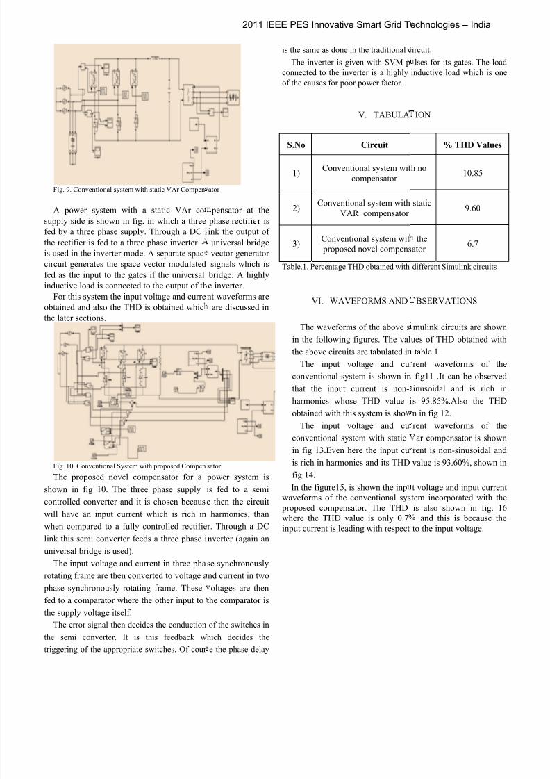
Fig. 9. Conventional system with static VAr Compen
A power system with a static VAr co
supply side is shown in fig. in which a three
fed by a three phase supply. Through a DC l
the rectifier is fed to a three phase inverter.
is used in the inverter mode. A separate spac
circuit generates the space vector modulated
fed as the input to the gates if the universalinductive load is connected to the output of th
For this system the input voltage and curre
obtained and also the THD is obtained whic
the later sections.
Fig. 10. Conventional System with proposed Compen
The proposed novel compensator for a
shown in fig 10. The three phase supply
controlled converter and it is chosen becaus
will have an input current which is rich in
when compared to a fully controlled rectifie
link this semi converter feeds a three phase i
universal bridge is used).
The input voltage and current in three pha
rotating frame are then converted to voltage a
phase synchronously rotating frame. These
fed to a comparator where the other input to
the supply voltage itself.
The error signal then decides the conduction
the semi converter. It is this feedback w
triggering of the appropriate switches. Of cour
2011 IEEE PES Innovative Smart Grid T
ator
pensator at the
phase rectifier is
ink the output of
universal bridge
vector generator
signals which is
bridge. A highlye inverter.
nt waveforms are
are discussed in
sator
power system is
is fed to a semi
e then the circuit
harmonics, than
r. Through a DC
nverter (again an
se synchronously
nd current in two
oltages are then
the comparator is
of the switches in
hich decides the
e the phase delay
is the same as done in the traditional c
The inverter is given with SVM p
connected to the inverter is a highly
of the causes for poor power factor.
V. TABULA
S.No Circuit
1)Conventional system wit
compensator
2)Conventional system with
VAR compensator
3)Conventional system wit
proposed novel compens
Table.1. Percentage THD obtained with
VI. WAVEFORMS AND
The waveforms of the above s
in the following figures. The val
the above circuits are tabulated i
The input voltage and cu
conventional system is shown in
that the input current is non-
harmonics whose THD value i
obtained with this system is sho
The input voltage and cu
conventional system with static
in fig 13.Even here the input cu
is rich in harmonics and its THD
fig 14.
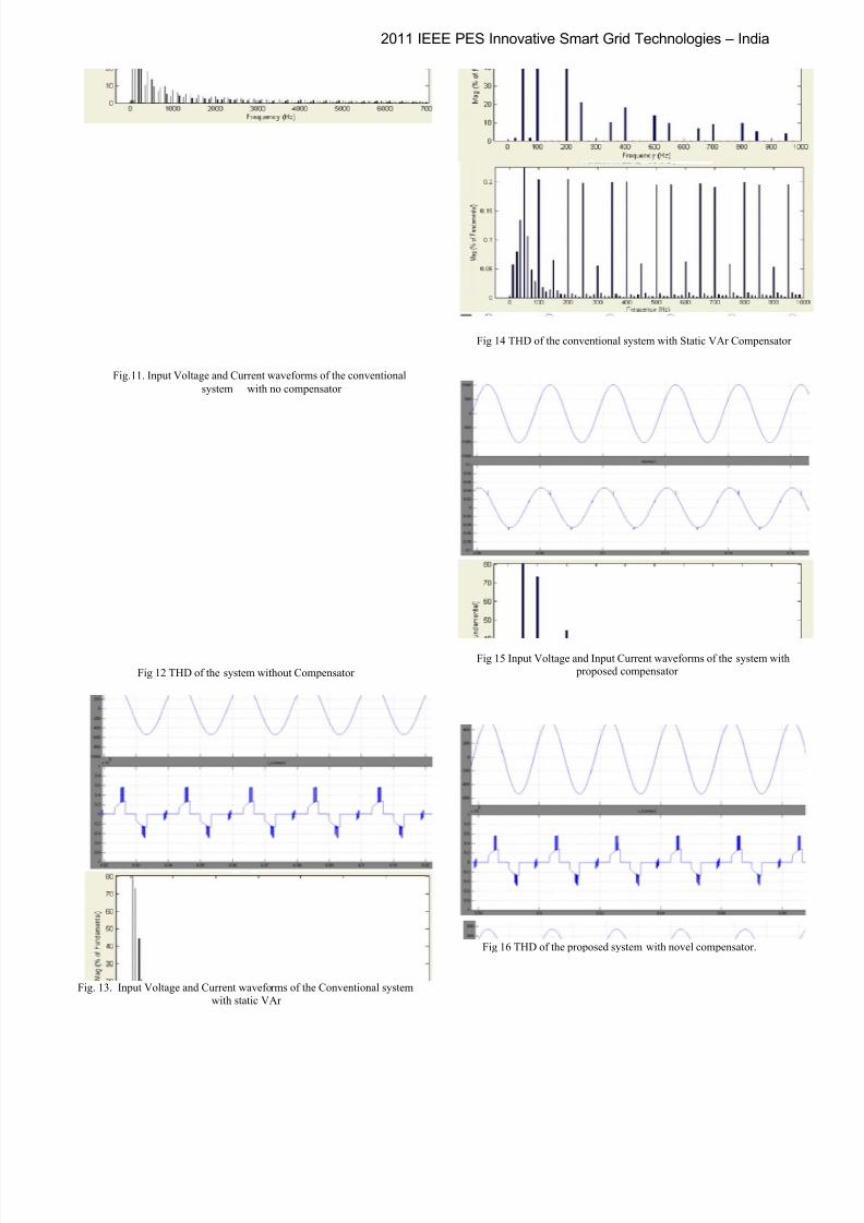
In the figure15, is shown the inp
waveforms of the conventional sys
proposed compensator. The THD
where the THD value is only 0.7
input current is leading with respect
echnologies – India
ircuit.
lses for its gates. The load
inductive load which is one
ION
% THD Values
h no10.85
static9.60
the
ator6.7
different Simulink circuits
BSERVATIONS
mulink circuits are shown
ues of THD obtained with
table 1.
rent waveforms of the
fig11 .It can be observed
inusoidal and is rich in
s 95.85%.Also the THD
n in fig 12.
rent waveforms of the
ar compensator is shown
rent is non-sinusoidal and
value is 93.60%, shown in
t voltage and input current
tem incorporated with the
is also shown in fig. 16
and this is because the
to the input voltage.
8/12/2019 Improvement o Fpf
http://slidepdf.com/reader/full/improvement-o-fpf 5/6
2011 IEEE PES Innovative Smart Grid Technologies – India
Fig.11. Input Voltage and Current waveforms of the conventional
system with no compensator
Fig 12 THD of the system without Compensator
Fig. 13. Input Voltage and Current waveforms of the Conventional system
with static VAr
Fig 14 THD of the conventional system with Static VAr Compensator
Fig 15 Input Voltage and Input Current waveforms of the system with proposed compensator
Fig 16 THD of the proposed system with novel compensator.

8/12/2019 Improvement o Fpf
http://slidepdf.com/reader/full/improvement-o-fpf 6/6
2011 IEEE PES Innovative Smart Grid Technologies – India
VII. CONCLUSIONS
A novel compensating technique for the improvement of
power factor in non-linear electrical systems such as power
electronic systems is presented in this paper. Vector control is
implemented at the supply side of the system. .The reactive
component of the supply current is set to zero which is then
compared with the actual reactive component of current that isdrawn by the system. With the closed loop control the system
starts drawing a leading current which implies that the power
factor is improved and so the Total Harmonic Distortion is
reduced. A conventional system, a conventional power system
with static Var Compensator, and a typical power system with
the proposed technique are simulated using MATLAB/
SIMULINK and the waveforms of input voltage and input
current and the THD for each of them are obtained and
compared. It is observed that with the proposed method, the
entire system starts drawing a leading current inspite of the
non-linear loads connected to the system(the system itself is a
non-linear one).The THD value is also found to be reduced toa great extent.
R EFERENCES
[1] Bimal K.Bose,” Modern Power Electronics and AC drives” PHI
publications 2005.
[2] Yongsug Suh, Valentin Tijeras, and Thomos A.Li “A Control method indq Synchronous Frame for PWM Boost Rectifier under Generalized
Unbalanced Operating conditions”, IEEE PESC
Conference,Queensland, Australia, June 23-27, 2002.[3] H Enjeti, P.N.Zioga. P.D.Lindsay.J.F. Rashid, M.H A new PWM speed
control system for high Performance AC motor drive “IEEE
Transactions on Industrial electronics, 1997.[4] Holtz.J; Springob L, “Reduced harmonics PWM controlled line-
side converts for electric drives”,IEEE transactions on Industry
applications. Volume 29, No.4, July 1993. PP 814-819.[5] Akagi,.H.—Kanazawa,Y.—Nabae, “Instantaneous Reactive Power
Compensators Comprising Switching Devices without Energy Storage
Components”, IEEE Trans on Ind. Appl. IA-20 No. 3 (May/June 1984).[6] Akagi,H.—Kanazawa,Y.—abae,A.,”Generalized Theory of the
Instantaneous Reactive Power in Three-Phase Circuits”, IPEC,
Tokyo’83, pp. 1375– 1386.Bowes, S. R.—Clements, R. R., “Computer Aided Design of PWM
Inverter Systems”, IEE. Proc.129, Pt. B No1 (Jan1982).
[7] Patel, H. S.—Hoft, R. G. “Generalized Technique of HarmonicElimination and Voltage Control in Thyristor Inverters Part I-Harmonic
Elimination”, IEEE Trans. On Ind. Appl. IA-9(May/ June 1973), 310–
317.


![Pakistan iSC Improvement Roadmap Final draft...D'& ^ >/ W/ ' ' ] o P ] r o ] v ',^ ]^ : : } ] v ] o](https://img.pdfslide.us/doc/110x75/5f416c2cd5498860566ca85e/pakistan-isc-improvement-roadmap-final-draft-d-w-o-p-.jpg)


![c 2014 Shane T. Ghiotto - Illinois: IDEALS Home · 2.1 Feedback Particle Filter In [16, 14], the algorithm for the feedback particle filter (FPF) was introduced. FPF is a novel algorithm](https://img.pdfslide.us/doc/110x75/5b904cfb09d3f2e6728babd7/c-2014-shane-t-ghiotto-illinois-ideals-home-21-feedback-particle-filter.jpg)