Embed Size (px)
Citation preview
1726 IEEE SENSORS JOURNAL, VOL. 11, NO. 8, AUGUST 2011
Improved Sensitivity of AlGaN/GaN FieldEffect Transistor Biosensors by Optimized
Surface FunctionalizationXuejin Wen, Michael L. Schuette, Samit Kumar Gupta, Theodore R. Nicholson, III, Stephen Craig Lee, and
Wu Lu, Senior Member, IEEE
Abstract—In this paper, we optimize the AlGaN surface oxida-tion methods for AlGaN/GaN heterostructure field effect transistor(HFET) biological sensors. Reactive ion etching oxygen plasma, in-ductively coupled oxygen plasma, and piranha solution are used tooxidize AlGaN surface. After oxidation, X-ray photoelectron spec-troscopy and water contact angle measurements are used to checkoxidation effectiveness. Labeled streptavidin (SA) molecules arebound to the oxidized surface through linker molecules for com-parison of surface modification effectiveness. Schottky diodes arefabricated to investigate the impacts of oxidation processes on elec-trical properties, such as Schottky barrier heights, sheet carrierconcentrations, and interface trap densities. The results show thatthe inductively coupled plasma oxidation process has a superiorbehavior compared to the reactive ion etching oxygen plasma andpiranha solution oxidation processes. AlGaN/GaN HFET proteinsensors fabricated using the inductively coupled plasma oxidationprocess have exhibited improved sensitivity. An SA solution withthe concentration as low as 4.73 pM were successfully detected.
Index Terms—Biosensor, field-effect transistor (FET), GaN, sur-face functionalization.
I. INTRODUCTION
AlGaN/GaN HFETs have demonstrated excellent power andhigh frequency performance for wireless and microwave ap-plications because of the high sheet carrier concentration inthe GaN channel at the AlGaN and GaN interface, the highsaturation velocity, and high breakdown field in GaN [1], [2].Transistors fabricated on the AlGaN/GaN material system canalso be used as high-sensitivity gas, chemical, and biologicalsensors because of the unique material and device properties
Manuscript received August 09, 2010; revised October 19, 2010; acceptedNovember 06, 2010. Date of publication November 29, 2010; date of currentversion May 25, 2011. This work was supported in part by the National ScienceFoundation under Grants ECCS-0702191, CBET-0756594, ECCS-0824170,CMMI-0928888, and OSU Institute for Materials Research. The work of W.Lu was supported by the WCU program by Korean Ministry of Education,Science, and Technology. The associate editor coordinating the review of thispaper and approving it for publication was Prof. E. H. Yang.
X. Wen and M. L. Schuette are with the Department of Electrical and Com-puter Engineering, The Ohio State University, Columbus, OH 43210 USA.
S. K. Gupta and T. R. Nicholson, III, are with the Department of Biomed-ical Engineering and the Dorothy Davis Heart and Lung Research Institute, TheOhio State University, Columbus, OH 43210 USA.
S. C. Lee is with the Department of Biomedical Engineering and the DorothyDavis Heart and Lung Research Institute, The Ohio State University, Columbus,OH 43210 USA, and also with the Department of Chemical Engineering, TheOhio State University, Columbus, OH 43210 USA.
Color versions of one or more of the figures in this paper are available onlineat http://ieeexplore.ieee.org.
Digital Object Identifier 10.1109/JSEN.2010.2095458
such as chemical inertness, non-toxicity, and high transconduc-tance gm [3]–[6]. For AlGaN/GaN HFET sensors, the opengate surface properties are critical for selectivity or specificity.For gas sensors, a catalytic metal thin film layer such as Ptor Pd is deposited as the catalyst for hydrogen detection [3].For ion-selective field-effect transistors (ISFET), the selectivityof ions is determined by the selection of the open gate sur-face materials [6], [7]. For biological sensors, surface modifi-cation and functionalization is critical for biomolecular immo-bilization and sensing specificity [4], [8], [9]. To immobilizebiomolecules on AlGaN/GaN surfaces, two typical strategieshave been used. One strategy is to deposit a thin metal film onthe AlGaN surface, e.g., Au or Ag, and link probe moleculesthrough a self-assembly process. A widely used process is tolink the gold surface to the molecules, one end of which is mod-ified with thiol groups and the other end is modified with spe-cific biological functional groups [10]. The other strategy is tooxidize the AlGaN surface and link the next layer of functionalmolecules to surface oxygen atoms by covalent bonding, i.e.,silane molecules [4]. These two strategies can be designed fordetection of different target molecules. From the device point ofview, the deposition of metals or surface oxidation has differentimpacts on the electrical properties of devices, e.g., carrier con-centration in the channel, surface morphology, and trap prop-erties on the semiconductor surfaces. In this paper, we system-atically investigate the impacts of different oxidation methodson AlGaN/GaN device electrical properties and detection sen-sitivity under the approach of protein detection through silanelinkers.
To immobilize probe molecules on electrical biosensors bycovalent bonding to oxygen atoms, an ideal surface oxidationprocess is expected to increase the surface reactivity to biolog-ical molecules, improve device electrical performance, and becompatible with the microelectronic fabrication processes. Tooxidize the AlGaN surface, there are a few candidate methodsthat can be implemented for evaluation. As a traditional wetchemical approach, piranha solution treatment on AlGaNsurface has demonstrated the capability of achieving oxidationand hydrophilicity at the same time, which is essential forsilanization [11]. On the other hand, plasma treatment hasalso been studied for biocompatibility. Reactive ion etching(RIE)/inductive-coupled plasma (ICP) treatments are widelyused in semiconductor device fabrication. RIE plasma gener-ally creates a high bias to the substrate or a high ion kineticenergy whereas ICP plasma generated under a high coil power
1530-437X/$26.00 © 2010 IEEE
WEN et al.: IMPROVED SENSITIVITY OF AlGaN/GaN FIELD EFFECT TRANSISTOR BIOSENSORS 1727
has a higher plasma density. With different gases and powerconditions, the plasma can be used for different purposes suchas ashing photoresist residues and etching materials selectively[12]. When oxygen plasma is used, it can also be used foroxidizing semiconductor surfaces, such as AlGaN [13]. Thesurface properties, such as morphology, hydrophilicity, charges,and traps etc., could be affected largely by these processes. Thesurface charges and surface potential can be changed by theintroduction of charged oxygen atoms. The barrier height ofSchottky diodes fabricated on these materials can be increasedor decreased which will affect the gate leakage current. Thetwo-dimensional electron gas (2DEG) carrier concentrationwill also be affected [14]. The properties of AlGaN surface trapstates can also be changed due to the plasma ion bombardment,which has large impacts on the device performance becausesurface and interface states can respond to the gate potential bycharging and discharging. For sensors, the chemical/biologicalspecies induced signals could be weakened, resulting in adecreased sensitivity. The dynamic response of the sensors isalso affected by traps that are introduced during the processing[15]. To achieve high sensor sensitivity, it is very important tooxidize AlGaN surface with minimum degradation of deviceperformance.
In this paper, we evaluate the effectiveness and impact oftechniques for oxidizing III-nitride materials for biosensing ap-plications. Three different methods of oxidation are character-ized by X-ray photoelectron spectroscopy (XPS), water contactangle, and Schottky diodes capacitance-voltage (C-V), and cur-rent-voltage (I-V) measurements. The chemical structures of ox-idized AlGaN surfaces are analyzed by XPS study [16], [17].Water contact angle measurement is used to compare the changeof AlGaN surface hydrophilicity which is important for silaniza-tion. The specificity and surface coverage are characterized byfluorescence images. An enzyme-linked immunosorbent assay(ELISA) is performed to quantitatively characterize the absorp-tion concentrations of SA on the functionalized AlGaN surfaces.C-V and I-V characteristics of AlGaN/GaN Schottky diodes areused for analysis of the electronic properties such as 2DEG den-sities, and surface and interface trap densities and lifetimes etc.The discussion of oxidation and trap properties is followed byelectrical detection results of SA solutions. The conclusions aresummarized last.
II. MATERIAL AND OXIDATION METHODS
A. Materials
For XPS, water contact angle, and fluorescence imagingcharacterization, Al Ga N wafer (TDII Inc.) with a thick-ness of 0.5 m and a Si doping concentration of cmon a (0001) SiC substrate. The Al concentration of this AlGaNlayer is the same with the AlGaN barrier of device AlGaN/GaNheterostructure to study the chemical properties for differentoxidation methods. Because of the low doping level, Si atomsshould not have an appreciable effect on the chemical prop-erties. For electrical devices such as Schottky diodes andbiosensor devices, AlGaN/GaN heterostructure structure wasused. The heterostructure was grown by metal-organic chem-ical-vapor deposition (MOCVD) on a (0001) SiC substrate. A
40 nm AlN nucleation layer was firstly grown on the substrate,followed by a 3 m undoped GaN buffer layer. A 23 nm un-doped Al Ga N layer was grown on the GaN layer to formthe heterostructure. Hall measurements at room temperatureshowed a sheet carrier density of cm and a carriermobility of 2100 cm V s.
B. Oxidization Methods
For piranha solution treatment, the sample was rinsed in pi-ranha solution made from H SO H O for 20 min-utes [11], rinsed in de-ionized (DI) water with ultrasonic agita-tion for 5 minutes, and blown dry by N . An Oxford PlasmaLab100 system was used to oxidize AlGaN surfaces at RIE and ICPmodes separately. For the RIE method, 25 W radio frequency(RF) power with a 5 mTorr chamber pressure, 50 sccm O and0 W ICP plasma coil power was applied. The plasma-inducedbias to substrate was 110 V. For ICP method, 1000 W ICPplasma coil power with 20 mTorr chamber pressure, 50-sccmO , and 0 W RF power was applied. For ICP treatment, thereis no bias induced between the plasma and substrate. The dura-tion of both RIE and ICP treatments was 30 seconds. The RIEplasma condition was optimized for minimum surface damageand with reasonable oxidation effects on sample surfaces. TheICP plasma condition was optimized for high-density oxygenplasma. The condition was chosen based on our experience foran AlGaN/GaN HFET gate recession process [12]. For compar-ison, together with an unoxidized reference sample, three dif-ferently oxidized AlGaN samples were studied by XPS, watercontact angle, fluorescence, ELISA, and diode measurements.The four samples are referred later in this paper as REF, PS,RIE, and ICP, respectively corresponding to nontreatment, pi-ranha solution, RIE plasma, and ICP plasma treatments.
C. XPS Measurements
For XPS study, the samples were transferred into an ultrahighvacuum (UHV) Kratos Axis Ultra XPS system chamber imme-diately after oxidation. Overnight vacuum pump was performedto achieve a base pressure of Torr before measure-ments. A monochromatic Al anode X-ray gun was used for de-tection of C 1s, Al 2p, Ga 3d, and Ga 2p peaks. C 1s peak wasaligned to 284.5 eV as a reference peak. A Mg anode X-ray gunwas used to measure O 1s and and Ga 2p peaks. Since deep levelGa 2p peak is not sensitive to oxidation, it is used as a referencepeak to align Mg anode activated peaks to Al anode activatedpeaks.
D. Water Contact Angle Measurements
For water contact angle measurements, four samples wereplaced separately on a horizontal flat stage. A syringe was usedto apply the same volume of de-ionized (DI) water drops ontoeach of the samples. The water profile image was captured im-mediately after the application of DI water drops, without no-ticeably evaporation. The contact angle is extracted from the im-ages with a developed Matlab program.
E. Diodes Fabrication and Measurements
For fabrication of Schottky diodes, Ti/Al/Ti/Au metal layerswere deposited with a lift-off process followed by rapid thermal
1728 IEEE SENSORS JOURNAL, VOL. 11, NO. 8, AUGUST 2011
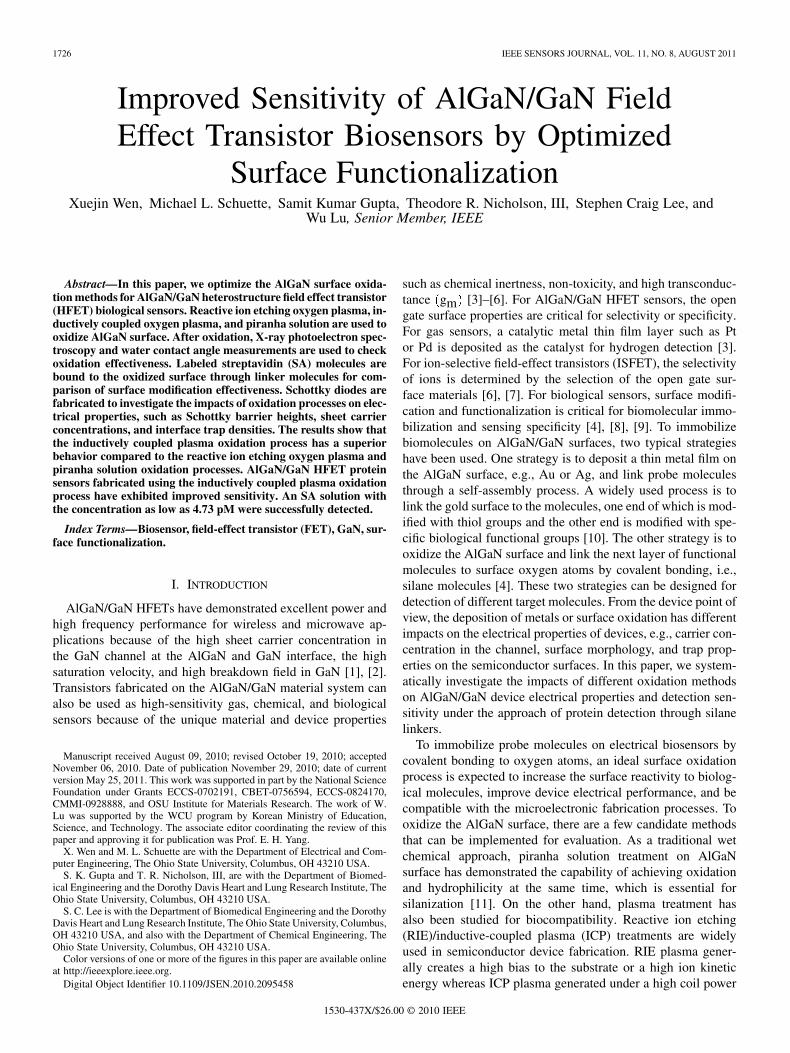
Fig. 1. (a) The molecular structure of modified AlGaN surface bonding with SA molecules. (b) The schematic of AlGaN/GaN HFET biosensor structure withtest setup.
annealing (RTA) to form Ohmic contacts. The devices werethen deposited with a 200 nm SiO layer. Schottky patternswere opened by a negative photoresist photolithography stepand etching of oxide layer in diluted HF. Photoresist were thenremoved and three of the samples were oxidized by piranha so-lution, RIE, and ICP methods separately while the fourth samplewas kept as the reference. During the treatment, only the openarea that is to be deposited by Schottky contacts was oxidizedwhile the rest area remains protected by the thick SiO film. TheSiO protection layer was then removed by diluted HF after theSchottky metal Ni/Au was deposited by another lift-off process.The fabricated diodes have a dimension of 120 m in diameter.After fabrication, I-V measurements were performed using anAgilent 4156C semiconductor parameter analyzer and C-V mea-surements were performed using an Agilent 4284 LCR meter.For C-V measurements, the frequency range was from 100 Hzto 1 MHz and the applied ac signal amplitude was 100 mV.
F. Biotinylation
To immobilize SA molecules, the treated AlGaN surfaceswere oxidized, silanized, and biotinylated [4]. During thesilanization step, the samples were deposited with 3-amino-propyltriethoxysilane (3-APTES) to modify the surface withamine groups. After oxidation, the samples were boiled inDI water for 30 min at 100 C and then blown dry by a ni-trogen gun. 2% 3-APTES in acetone was used to treat thesamples for 30 min. The silanized samples were washed inacetone, propanol, dried by nitrogen gun and then baked at120 C for 5 min. For biotinylation, Sulfo-NHS-biotin (PierceBiotechnology, Rockford, IL) was dissolved in DI water ata concentration of 1 mg/ml. The solution was dropped tosilanized AlGaN surfaces and covered by a glass slide to spreadthe solution all over the sample surfaces. The samples werethen incubated in a humid chamber to avoid evaporation atroom temperature. After 2 hours, the samples were rinsed inPBS three times and immersed in superblock buffer (PierceBiotechnology, Rockford, IL) for 1 hour to block the exposedarea where the APTES or Sulfo-NHS-biotin coverage wasnot complete. After biotinylation, the modified surfaces are
ready to bind with SA molecules. The molecular structure withbinding to SA molecules is shown in Fig. 1(a).
G. Protein Binding and Detection on AlGaN Surface
SA labeled by Alexa Fluor 488 in PBS solution was usedfor fluorescent imaging. AlGaN samples that experienced nospecial oxidation protocol (i.e., with only native oxide, REF),and experienced ICP, RIE, and PS oxidations were 3-APTEStreated and biotinylated, as described. Drops of 10 mg/ml SA(Pierce Biotechnology, Rockford, IL) in PBS were placed onbiotinylated AlGaN surfaces and incubated at room tempera-ture for 20 min. The samples were rinsed exhaustively withPBS to remove any unbound SA molecules. A second set of3-APTES-treated AlGaN samples were left unbiotinylated, butthereafter treated exactly as above to determine background flu-orescence/SA binding in the absence of biotin on the polymerfilm. After capture of fluorescent images of AlGaN chips treatedwith SA labeled by Alexa Fluor 488 as photomicrographs, aMatlab program was used to determine the average intensity ofthe florescent images. Fluorescence data are presented as unit-less ratios of the fluorescence intensity of 3-APTES-treated, bi-otinylated (ICP, RIE, PS oxidized or with native oxide, REF)to identically oxidized samples that had been silane and SAtreated, but not biotinylated.
In preparation for an ELISA, AlGaN wafers were diced intochips and treated with the three oxidation protocols: ICP, RIE,and PS. Chips were treated for biotinylation as described exceptthat the chips were incubated for 50 min with 2% 3-APTES,incubated for 2 hours at 37 C with 10 mg/ml sulfo-NHS-biotinand superblock was omitted. Chips were then treated with 10
g/ml streptavidin (Pierce Biotechnology, Rockford, IL) for30 min at 37 C, rinsed three times in PBS containing 0.1%Tween-20, and placed in a solution of biotinylated horseradishperoxidase (biotin-HRP) (Pierce Biotechnology, Rockford, IL)at 1 g/ml for 30 min. Following rinsing three times in 0.1%Tween-20 PBS, chips were incubated in the dark for 20 minwith the enzymatic substrate for biotin-HRP, -phenylene-diamine (Sigma-Aldrich, St. Louis, MO). The reaction wasstopped using 3 M H SO and the absorbance was read at 492
WEN et al.: IMPROVED SENSITIVITY OF AlGaN/GaN FIELD EFFECT TRANSISTOR BIOSENSORS 1729
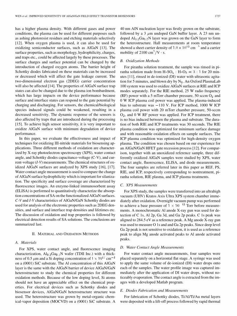
Fig. 2. XPS Ga3d spectra and de-convoluted Ga–O, Ga–N, and N 2s peaks of samples oxidized by three different methods. The increase of Ga–O peak areascompared to REF sample indicates that surface Al atoms are oxidized by all the methods.
nm using the Victor X3 Multilabel Plate Reader (PerkinElmer,Waltham, MA). Absorbance data was then normalized usingindividual chip surface area in m .
H. HFET Biosensor Fabrication
The device isolation of AlGaN/GaN HFET biosensors wasobtained by chlorine-based plasma dry etching. The Ohmiclayer formation is the same as described in diodes fabrication.A Ni/Au overlay layer was deposited by a lift-off process foron-wafer probing measurements. A silicone layer was appliedto form the reservoir for solutions as well as to isolate elec-trodes from buffer solution. The open gate dimension is 2 mmwide and 1 mm long. The cross-sectional view of the devicestructure, as well as the test setup, is shown in Fig. 1(b).
III. RESULTS AND DISCUSSIONS
A. XPS Characteristics
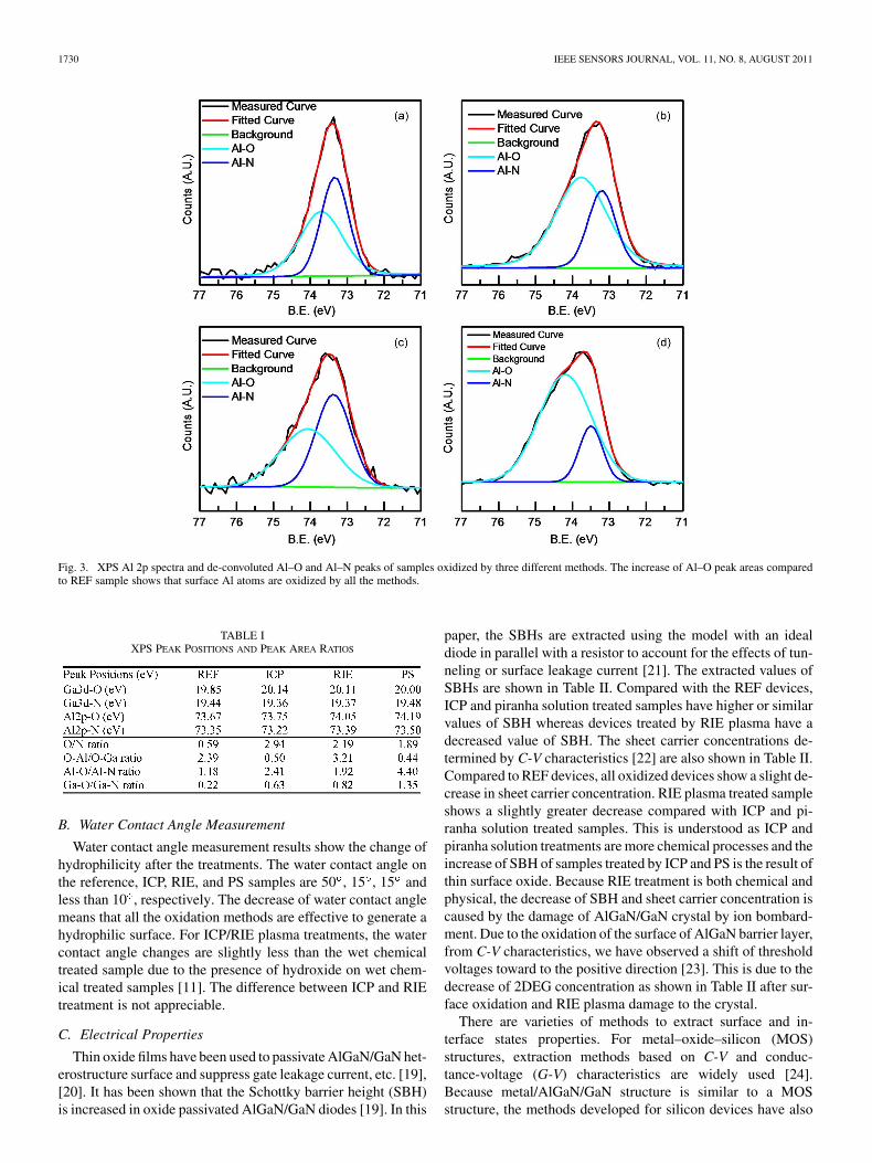
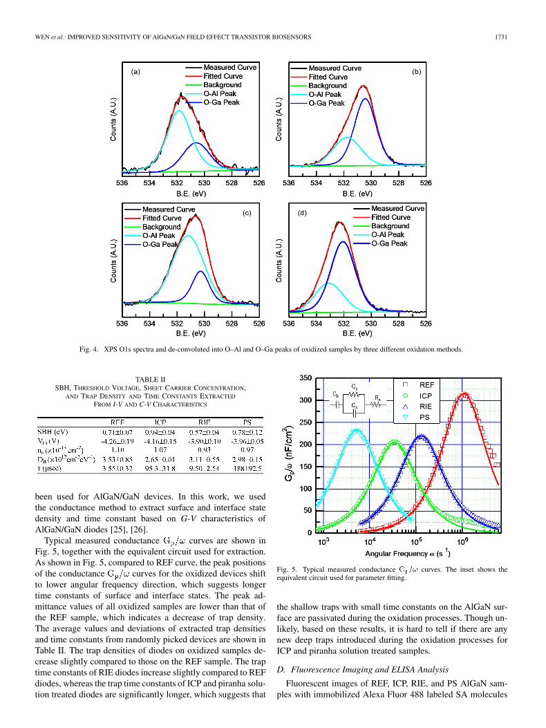
The core level electron spectra are shown in Figs. 2 and 3. Ga3d peaks are de-convoluted into Ga-O, Ga-N, and N 1s peaks[18] and Al 2p peaks are de-convoluted into peaks of Al–O andAl–N bonds. The de-convoluted peak positions and the area ra-tios are summarized in Table I. As shown in the table, both theGa 3d(O) and Al 2p(O) peak areas increased for all the oxidizedsamples compared to the REF sample. The ratios of O 1s/N 1s,Ga 3d(O)/Ga 3d (N) and Al 2p(O)/Al 2p(N) increased comparedto the REF sample, suggesting that the oxide fraction increasedwhereas nitride fraction decreased and oxidation of both Ga
and Al elements happened for all the oxidation methods. FromTable I, the peak positions of Ga 3d(O) and Al 2p(O) shift tohigher bonding energy, indicating that the newly formed oxideshave higher bonding energy than native oxide. The Ga 3d(N)and Al 2p(N) positions remain constant for all samples.
As shown in Fig. 4, the O 1s spectra are de-convoluted intoO 1s(Ga) and O 1s(Al) bonding peaks. As shown in Table I, thepeak area ratio change between O 1s(Al) and O 1s(Ga) bondsshows clear differences for different oxidation methods, sug-gesting that surface Al and Ga atoms are oxidized at differentratios because of different oxidation mechanisms. For ICP andpiranha solution treated samples, O 1s(Al)/O 1s(Ga) ratio de-creases whereas for RIE treated sample, O 1s(Al)/O 1s(Ga) ratioincreases. This suggests that on the ICP and piranha solutiontreated samples, there is more gallium oxide formed whereas onthe RIE treated sample there is more aluminum oxide formed.Under the coupling between ICP coil and plasma, since theplasma induced substrate bias is essentially zero at zero RFpower, there is no physical ion bombardment process during theoxidation process by the high density plasma. Hence, the oxi-dation is more chemical and isotropic [12], which is somewhatsimilar to the wet chemical treatment process. For RIE treat-ment, the dc bias between plasma and substrate is induced. Theoxygen ions in plasma are accelerated by the bias to substrate togain kinetic energy. Therefore, the AlGaN surface experiencesion bombardment as well as oxidation. Because gallium oxideis more volatile than aluminum oxide, with high kinetic oxygenions bombardment, some of the gallium oxide was sputtered andevacuated. As a result, there exists more Al oxide on the surface.
1730 IEEE SENSORS JOURNAL, VOL. 11, NO. 8, AUGUST 2011
Fig. 3. XPS Al 2p spectra and de-convoluted Al–O and Al–N peaks of samples oxidized by three different methods. The increase of Al–O peak areas comparedto REF sample shows that surface Al atoms are oxidized by all the methods.
TABLE IXPS PEAK POSITIONS AND PEAK AREA RATIOS
B. Water Contact Angle Measurement
Water contact angle measurement results show the change ofhydrophilicity after the treatments. The water contact angle onthe reference, ICP, RIE, and PS samples are 50 , 15 , 15 andless than 10 , respectively. The decrease of water contact anglemeans that all the oxidation methods are effective to generate ahydrophilic surface. For ICP/RIE plasma treatments, the watercontact angle changes are slightly less than the wet chemicaltreated sample due to the presence of hydroxide on wet chem-ical treated samples [11]. The difference between ICP and RIEtreatment is not appreciable.
C. Electrical Properties
Thin oxide films have been used to passivate AlGaN/GaN het-erostructure surface and suppress gate leakage current, etc. [19],[20]. It has been shown that the Schottky barrier height (SBH)is increased in oxide passivated AlGaN/GaN diodes [19]. In this
paper, the SBHs are extracted using the model with an idealdiode in parallel with a resistor to account for the effects of tun-neling or surface leakage current [21]. The extracted values ofSBHs are shown in Table II. Compared with the REF devices,ICP and piranha solution treated samples have higher or similarvalues of SBH whereas devices treated by RIE plasma have adecreased value of SBH. The sheet carrier concentrations de-termined by C-V characteristics [22] are also shown in Table II.Compared to REF devices, all oxidized devices show a slight de-crease in sheet carrier concentration. RIE plasma treated sampleshows a slightly greater decrease compared with ICP and pi-ranha solution treated samples. This is understood as ICP andpiranha solution treatments are more chemical processes and theincrease of SBH of samples treated by ICP and PS is the result ofthin surface oxide. Because RIE treatment is both chemical andphysical, the decrease of SBH and sheet carrier concentration iscaused by the damage of AlGaN/GaN crystal by ion bombard-ment. Due to the oxidation of the surface of AlGaN barrier layer,from C-V characteristics, we have observed a shift of thresholdvoltages toward to the positive direction [23]. This is due to thedecrease of 2DEG concentration as shown in Table II after sur-face oxidation and RIE plasma damage to the crystal.
There are varieties of methods to extract surface and in-terface states properties. For metal–oxide–silicon (MOS)structures, extraction methods based on C-V and conduc-tance-voltage (G-V) characteristics are widely used [24].Because metal/AlGaN/GaN structure is similar to a MOSstructure, the methods developed for silicon devices have also
WEN et al.: IMPROVED SENSITIVITY OF AlGaN/GaN FIELD EFFECT TRANSISTOR BIOSENSORS 1731
Fig. 4. XPS O1s spectra and de-convoluted into O–Al and O–Ga peaks of oxidized samples by three different oxidation methods.
TABLE IISBH, THRESHOLD VOLTAGE, SHEET CARRIER CONCENTRATION,
AND TRAP DENSITY AND TIME CONSTANTS EXTRACTED
FROM I-V AND C-V CHARACTERISTICS
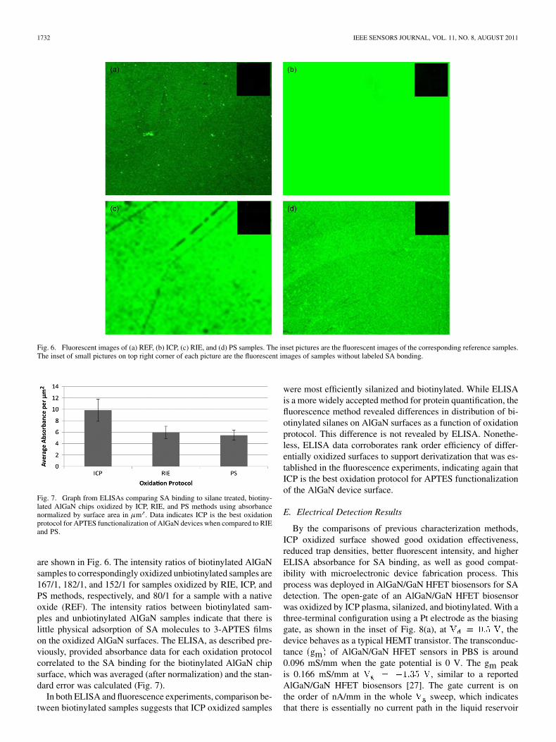
been used for AlGaN/GaN devices. In this work, we usedthe conductance method to extract surface and interface statedensity and time constant based on G-V characteristics ofAlGaN/GaN diodes [25], [26].
Typical measured conductance curves are shown inFig. 5, together with the equivalent circuit used for extraction.As shown in Fig. 5, compared to REF curve, the peak positionsof the conductance curves for the oxidized devices shiftto lower angular frequency direction, which suggests longertime constants of surface and interface states. The peak ad-mittance values of all oxidized samples are lower than that ofthe REF sample, which indicates a decrease of trap density.The average values and deviations of extracted trap densitiesand time constants from randomly picked devices are shown inTable II. The trap densities of diodes on oxidized samples de-crease slightly compared to those on the REF sample. The traptime constants of RIE diodes increase slightly compared to REFdiodes, whereas the trap time constants of ICP and piranha solu-tion treated diodes are significantly longer, which suggests that
Fig. 5. Typical measured conductance � �� curves. The inset shows theequivalent circuit used for parameter fitting.
the shallow traps with small time constants on the AlGaN sur-face are passivated during the oxidation processes. Though un-likely, based on these results, it is hard to tell if there are anynew deep traps introduced during the oxidation processes forICP and piranha solution treated samples.
D. Fluorescence Imaging and ELISA Analysis
Fluorescent images of REF, ICP, RIE, and PS AlGaN sam-ples with immobilized Alexa Fluor 488 labeled SA molecules
1732 IEEE SENSORS JOURNAL, VOL. 11, NO. 8, AUGUST 2011
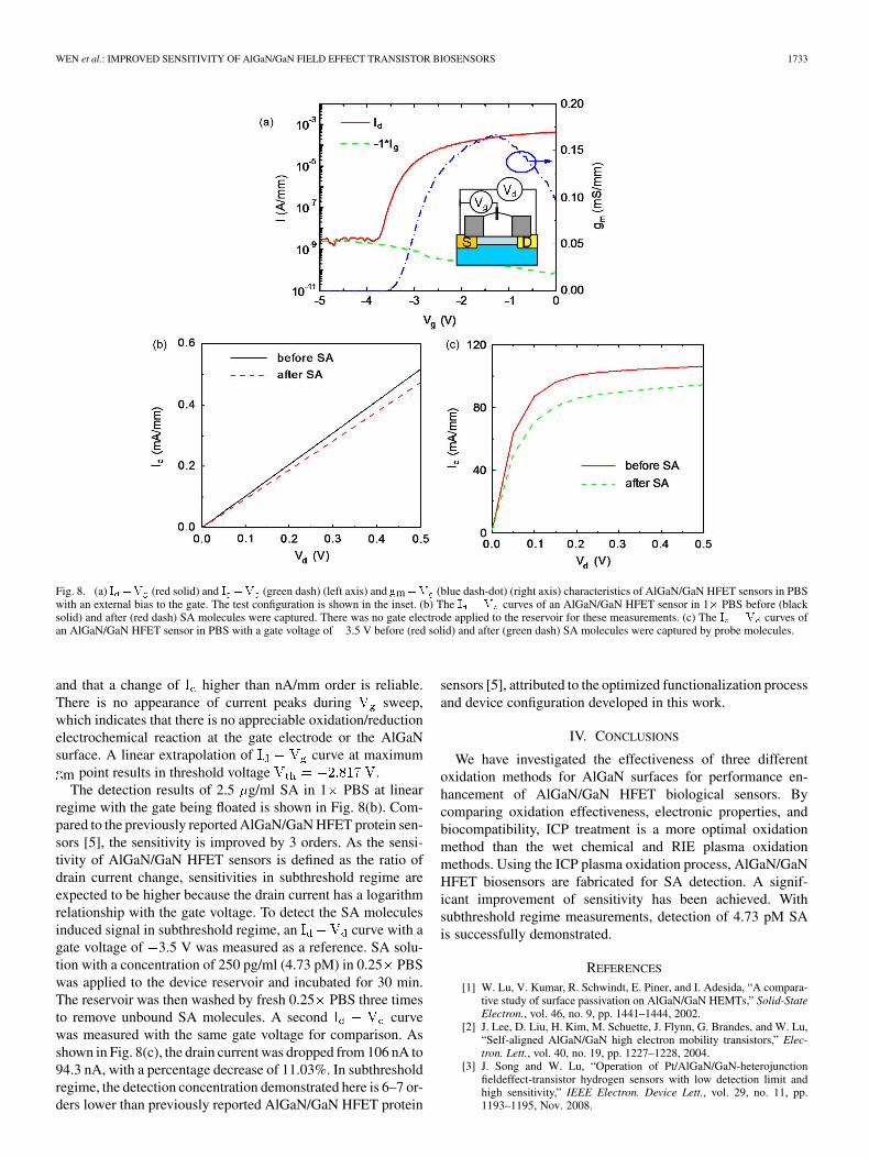
Fig. 6. Fluorescent images of (a) REF, (b) ICP, (c) RIE, and (d) PS samples. The inset pictures are the fluorescent images of the corresponding reference samples.The inset of small pictures on top right corner of each picture are the fluorescent images of samples without labeled SA bonding.
Fig. 7. Graph from ELISAs comparing SA binding to silane treated, biotiny-lated AlGaN chips oxidized by ICP, RIE, and PS methods using absorbancenormalized by surface area in �m . Data indicates ICP is the best oxidationprotocol for APTES functionalization of AlGaN devices when compared to RIEand PS.
are shown in Fig. 6. The intensity ratios of biotinylated AlGaNsamples to correspondingly oxidized unbiotinylated samples are167/1, 182/1, and 152/1 for samples oxidized by RIE, ICP, andPS methods, respectively, and 80/1 for a sample with a nativeoxide (REF). The intensity ratios between biotinylated sam-ples and unbiotinylated AlGaN samples indicate that there islittle physical adsorption of SA molecules to 3-APTES filmson the oxidized AlGaN surfaces. The ELISA, as described pre-viously, provided absorbance data for each oxidation protocolcorrelated to the SA binding for the biotinylated AlGaN chipsurface, which was averaged (after normalization) and the stan-dard error was calculated (Fig. 7).
In both ELISA and fluorescence experiments, comparison be-tween biotinylated samples suggests that ICP oxidized samples
were most efficiently silanized and biotinylated. While ELISAis a more widely accepted method for protein quantification, thefluorescence method revealed differences in distribution of bi-otinylated silanes on AlGaN surfaces as a function of oxidationprotocol. This difference is not revealed by ELISA. Nonethe-less, ELISA data corroborates rank order efficiency of differ-entially oxidized surfaces to support derivatization that was es-tablished in the fluorescence experiments, indicating again thatICP is the best oxidation protocol for APTES functionalizationof the AlGaN device surface.
E. Electrical Detection Results
By the comparisons of previous characterization methods,ICP oxidized surface showed good oxidation effectiveness,reduced trap densities, better fluorescent intensity, and higherELISA absorbance for SA binding, as well as good compat-ibility with microelectronic device fabrication process. Thisprocess was deployed in AlGaN/GaN HFET biosensors for SAdetection. The open-gate of an AlGaN/GaN HFET biosensorwas oxidized by ICP plasma, silanized, and biotinylated. With athree-terminal configuration using a Pt electrode as the biasinggate, as shown in the inset of Fig. 8(a), at , thedevice behaves as a typical HEMT transistor. The transconduc-tance gm of AlGaN/GaN HFET sensors in PBS is around0.096 mS/mm when the gate potential is 0 V. The gm peakis 0.166 mS/mm at , similar to a reportedAlGaN/GaN HFET biosensors [27]. The gate current is onthe order of nA/mm in the whole sweep, which indicatesthat there is essentially no current path in the liquid reservoir
WEN et al.: IMPROVED SENSITIVITY OF AlGaN/GaN FIELD EFFECT TRANSISTOR BIOSENSORS 1733
Fig. 8. (a) � �� (red solid) and � �� (green dash) (left axis) and �m�� (blue dash-dot) (right axis) characteristics of AlGaN/GaN HFET sensors in PBSwith an external bias to the gate. The test configuration is shown in the inset. (b) The � � � curves of an AlGaN/GaN HFET sensor in 1� PBS before (blacksolid) and after (red dash) SA molecules were captured. There was no gate electrode applied to the reservoir for these measurements. (c) The � � � curves ofan AlGaN/GaN HFET sensor in PBS with a gate voltage of �3.5 V before (red solid) and after (green dash) SA molecules were captured by probe molecules.
and that a change of higher than nA/mm order is reliable.There is no appearance of current peaks during sweep,which indicates that there is no appreciable oxidation/reductionelectrochemical reaction at the gate electrode or the AlGaNsurface. A linear extrapolation of curve at maximumm point results in threshold voltage .The detection results of 2.5 g/ml SA in 1 PBS at linear
regime with the gate being floated is shown in Fig. 8(b). Com-pared to the previously reported AlGaN/GaN HFET protein sen-sors [5], the sensitivity is improved by 3 orders. As the sensi-tivity of AlGaN/GaN HFET sensors is defined as the ratio ofdrain current change, sensitivities in subthreshold regime areexpected to be higher because the drain current has a logarithmrelationship with the gate voltage. To detect the SA moleculesinduced signal in subthreshold regime, an curve with agate voltage of 3.5 V was measured as a reference. SA solu-tion with a concentration of 250 pg/ml (4.73 pM) in 0.25 PBSwas applied to the device reservoir and incubated for 30 min.The reservoir was then washed by fresh 0.25 PBS three timesto remove unbound SA molecules. A second curvewas measured with the same gate voltage for comparison. Asshown in Fig. 8(c), the drain current was dropped from 106 nA to94.3 nA, with a percentage decrease of 11.03%. In subthresholdregime, the detection concentration demonstrated here is 6–7 or-ders lower than previously reported AlGaN/GaN HFET protein
sensors [5], attributed to the optimized functionalization processand device configuration developed in this work.
IV. CONCLUSIONS
We have investigated the effectiveness of three differentoxidation methods for AlGaN surfaces for performance en-hancement of AlGaN/GaN HFET biological sensors. Bycomparing oxidation effectiveness, electronic properties, andbiocompatibility, ICP treatment is a more optimal oxidationmethod than the wet chemical and RIE plasma oxidationmethods. Using the ICP plasma oxidation process, AlGaN/GaNHFET biosensors are fabricated for SA detection. A signif-icant improvement of sensitivity has been achieved. Withsubthreshold regime measurements, detection of 4.73 pM SAis successfully demonstrated.
REFERENCES
[1] W. Lu, V. Kumar, R. Schwindt, E. Piner, and I. Adesida, “A compara-tive study of surface passivation on AlGaN/GaN HEMTs,” Solid-StateElectron., vol. 46, no. 9, pp. 1441–1444, 2002.
[2] J. Lee, D. Liu, H. Kim, M. Schuette, J. Flynn, G. Brandes, and W. Lu,“Self-aligned AlGaN/GaN high electron mobility transistors,” Elec-tron. Lett., vol. 40, no. 19, pp. 1227–1228, 2004.
[3] J. Song and W. Lu, “Operation of Pt/AlGaN/GaN-heterojunctionfieldeffect-transistor hydrogen sensors with low detection limit andhigh sensitivity,” IEEE Electron. Device Lett., vol. 29, no. 11, pp.1193–1195, Nov. 2008.
1734 IEEE SENSORS JOURNAL, VOL. 11, NO. 8, AUGUST 2011
[4] S. Gupta, M. Elias, X. Wen, J. Shapiro, L. Brillson, W. Lu, and S. C.Lee, “Detection of clinically relevant levels of protein analyte underphysiologic buffer using planar field effect transistors,” Biosens. Bio-electron., vol. 24, no. 4, pp. 505–511, 2008.
[5] B. S. Kang, F. Ren, L. Wang, C. Lofton, W. W. Tan, S. J. Pearton,A. Dabiran, A. Osinsky, and P. P. Chow, “Electrical detection of im-mobilized proteins with ungated AlGaN/GaN high-electron-mobilitytransistors,” Appl. Phys. Lett., vol. 87, no. 2, p. 023508, 2005.
[6] G. Steinhoff, M. Hermann, W. J. Schaff, L. F. Eastman, M. Stutzmann,and M. Eickhoff, “pH response of GaN surfaces and its application forpH-sensitive field-effect transistors,” Appl. Phys. Lett., vol. 83, no. 1,pp. 177–179, 2003.
[7] K. Izutsu and H. Yamamoto, “Response of an iridium comparison withother oxide pH sensor in pH-sensors nonaqueous solutions. Compar-ison with other oxide pH-sensors,” Anal. Sci., vol. 12, pp. 905–909,1996.
[8] G. Steinhoff, O. Purrucker, M. Tanaka, M. Stutzmann, and M. Eick-hoff, “AlxGa1-xN—A new material system for biosensors,” Adv.Funct. Mater., vol. 13, pp. 841–846, 2003.
[9] I. Cimalla, F. Will, K. Tonisch, M. Niebelschuz, V. Cimalla, V. Lebedev,G. Kittler, M. Himmerlich, S. Krischok, J. Schaefer, M. Gebinoga, A.Schober, T. Friedrich, and O. Ambacher, “AlGaN/GaN biosensor-ef-fect of device processing steps on the surface properties and biocompat-ibility,” Sens. Actuators, B, vol. 123, no. 2, pp. 740–748, 2007.
[10] B. S. Kang, S. J. Pearton, J. J. Chen, F. Ren, J. W. Johnson, R. J.Therrien, P. Rajagopal, J. C. Roberts, E. L. Piner, and K. J. Linthicum,“Electrical detection of deoxyribonucleic acid hybridization withAlGaN/GaN high electron mobility transistors,” Appl. Phys. Lett., vol.89, no. 12, p. 122102, 2006.
[11] B. Baur, G. Steinhoff, J. Hernando, O. Purrucker, M. Tanaka, B. Nickel,M. Stutzmann, and M. Eickhoff, “Chemical functionalization of GaNand AlN surfaces,” Appl. Phys. Lett., vol. 87, no. 26, p. 263901, 2005.
[12] M. L. Schuette and W. Lu, “Highly selective zero-bias plasma etchingof GaN over AlGaN,” J. Vac. Sci. Technol. B, vol. 25, pp. 1870–1874,2007.
[13] R. Dimitrov, V. Tilak, W. Yeo, B. Green, H. Kim, J. Smart, E.Chumbes, J. R. Shealy, W. Schaff, L. F. Eastman, C. Miskys, O. Am-bacher, and M. Stutzmann, “Influence of oxygen and methane plasmaon the electrical properties of undoped AlGaN/GaN heterostructuresfor high power transistors,” Solid-State Electron., vol. 44, no. 8, pp.1361–1365, 2000.
[14] D. Mistele, O. Katz, A. Horn, G. Bahir, and J. Salzman, “Impact ofnative oxides beneath the gate contact of AlGaN/GaN HFET devices,”Phys. Stat. Sol. (c), vol. 2, no. 7, pp. 2627–2630, 2005.
[15] G. Meneghesso, G. Verzellesi, R. Pierobon, F. Rampazzo, A. Chini,U. K. Mishra, C. Canali, and E. Zanoni, “Surface-related drain currentdispersion effects in AlGaN/GaN HEMTs,” IEEE Trans. Electron. De-vices, vol. 51, pp. 1554–1561, Oct. 2004.
[16] N. J. Watkins, G. W. Wicks, and Y. Gao, “Oxidation study of GaNusing X-ray photoemission spectroscopy,” Appl. Phys. Lett., vol. 75,no. 17, pp. 2602–2604, 1999.
[17] T. Hashizume, S. Ootomo, S. Oyama, M. Konishi, and H. Hasegawa,“Chemistry and electrical properties of surfaces of GaN andGaN/AlGaN heterostructures,” J. Vac. Sci. Technol. B, vol. 19(4),no. 4, pp. 1675–1681, 2001.
[18] T. Hashizume and H. Hasegawa, “Effects of nitrogen deficiency onelectronic properties of AlGaN surfaces subjected to thermal andplasma processes,” Appl. Surf. Sci., vol. 234, pp. 387–394, 2004.
[19] T. Hashizume, S. Ootomo, and H. Hasegawa, “Al2O3-based surfacepassivation and insulated gate structure for AlGaN/GaN HFETs,” Phys.Stat. Sol. (c), vol. 7, pp. 2380–2384, 2003.
[20] B. P. Gila, M. Hlad, A. H. Onstine, R. Frazier, G. T. Thaler, A. Her-rero, E. Lambers, C. R. Abernathy, S. J. Pearton, T. Anderson, S. Jang,F. Ren, N. Moser, R. C. Fitch, and M. Freund, “Improved oxide passi-vation of AlGaN/GaN high electron mobility transistors,” Appl. Phys.Lett., vol. 87, no. 16, p. 163503, 2005.
[21] M. L. Schuette and W. Lu, “Electrical transport in the copper ger-manide-n-GaN system: Experiment and numerical model,” J. Appl.Phys., vol. 101, no. 11, p. 113702, 2007.
[22] Z. Lin, W. Lu, J. Lee, D. Liu, J. S. Flynn, and G. R. Brandes, “Barrierheights of schottky contacts on strained AlGaN/GaN heterostructures:Determination and effect of metal work functions,” Appl. Phys. Lett.,vol. 82, no. 24, pp. 4364–4366, 2003.
[23] B. Green, K. Chu, E. Chumbes, J. Smart, J. Shealy, and L. Eastman,“The effect of surface passivation on the microwave characteristics ofundoped AlGaN/GaN HEMTs,” IEEE Electron. Device Lett., vol. 21,no. 6, pp. 268–270, Jun. 2000.
[24] D. K. Schroder, Semiconductor Material and Device Characteriza-tion. New York: Wiley-IEEE press, 2006, ch. 6.
[25] E. J. Miller, X. Z. Dang, H. H. Wieder, P. M. Asbeck, E. T. Yu, G.J. Sullivan, and J. M. Redwing, “Trap characterization by gate-drainconductance and capacitance dispersion studies of an AlGaN/GaN het-erostructure field-effect transistor,” J. Appl. Phys., vol. 87, no. 11, pp.8070–8073, 2000.
[26] R. M. Chu, Y. G. Zhou, K. J. Chen, and K. M. Lau, “Admittance charac-terization and analysis of trap states in AlGaN/GaN heterostructures,”Phys. Stat. Sol. (c), vol. 0, pp. 2400–2403, 2003.
[27] G. Steinhoff, B. Baur, G. Wrobel, S. Ingebrandt, A. Offenhausser, A.Dadgar, A. Krost, M. Stutzmann, and M. Eickhoff, “Recording of cellaction potentials with AlGaN/GaN field-effect transistors,” Appl. Phys.Lett., vol. 86, no. 3, p. 033901, 2005.
Xuejin Wen was born in Hubei, China, in 1979.He received the B.S. and M.S. degree in opticalengineering from Zhejiang University, Hangzhou, China. He is currently pursuing the Ph.D. degreein the Department of Electrical and ComputerEngineering, The Ohio State University, Columbus.
His research interests include GaN- and Si-basedelectrical biosensors for low-concentration pro-tein and DNA detection, bioelectronic devices forbiomedical applications, novel plasmonic devices,and nano-fabrication.
Michael L. Schuette was born in Delaware, Ohio, in1979. He received the B.S. degree in electrical engi-neering from Ohio Northern University, Ada, in 2002and the Ph.D. degree in electrical engineering fromThe Ohio State University, Columbus, in 2010.
At Ohio State, he studied GaN-based high elec-tron mobility transistor scaling as well as nanofab-rication. Since 2010, he has been at TriQuint Semi-conductor, Richardson, TX, where he continues todevelop deeply scaled GaN-based microwave tran-sistors. His other interests include electronic material
characterization, plasma processing, and electron-beam lithography.
Samit Kumar Gupta received the B.S. degree in computer engineering (withhonors) from the University of Maryland, College Park, in 2006 and the Ph.D.degree in biomedical engineering from The Ohio State University, Columbus,in 2010.
His research interests including field-effect-transistor biosensors, in vivo pro-tein detection, and nanobiotechnology. He has published work in Biosensorsand Bioelectronics, Journal of the Royal Society: Interface, and others and hasalso provided review services for Applied Physics Letters and Biosensors andBioelectronics.
Dr. Gupta is a current member of the Biomedical Engineering Society andAmerican Chemical Society.
Theodore R. Nicholson III received the B.S. degreein chemistry from Oakwood College, Huntsville, AL,in 2004. He is currently pursuing the Ph.D. degree atThe Ohio State University, Columbus, in the Biomed-ical Engineering Department where his field of re-search is biomedical nanotechnology and biomedicalmicrodevices.
Currently, he is working on the development of aprotein sensing device that will be used for real-timedetection of native proteins of interest via theirelectrical properties at the Davis Heart and Lung
Research Institute on the Ohio State University Medical Center campus.Mr. Nicholson III is a student member of the Biomedical Engineering Society.
WEN et al.: IMPROVED SENSITIVITY OF AlGaN/GaN FIELD EFFECT TRANSISTOR BIOSENSORS 1735
Stephen Craig Lee was born in Davenport, IA,on August 11, 1956. He received the B.S. degreein biology and chemistry from St. Ambrose Col-lege, Davenport,s in 1978 and the Ph.D. degree inmicrobiology from the University of Minnesota,Minneapolis, in 1984.
He served a postdoctoral fellowship in the Depart-ment of Genetics, Leland J. Stanford University, PaloAlto, CA, from 1984 to 1989, after which he wasemployed at Pharmacia Corporation (and its variousheritage companies), until 2001, when he joined The
Ohio State University, Columbus, as an Associate Professor of BiomedicalEngineering. He has served on numerous journal editorial boards includingthat of Biomedical Microdevices (2001–2009) as well as the editorial boards ofThe Journals of Biomedical Nanotechnology, The Journal of Nanoengineeringand Nanosystems-Part N, The Open Biotechnology Journal, and CurrentNanoscience, all of which he currently serves. His primary expertise resides inprotein engineering, genetics, and bioconjugate chemistry, which he applies tothe incorporation of protein functional components into nanoscale devices andstructures.
Dr. Lee is a past member of the American Society for Microbiology, and acurrent member of the Biomedical Engineering Society.
Wu Lu (M’97–SM’01) received the Ph.D. degree inphysical electronics and optoelectronics from South-east University, Nanjing, China, in 1994.
He is currently a tenured Associate Professorof the Department of Electrical and ComputerEngineering, The Ohio State University (OSU),Columbus. Before he joined OSU, he was a Post-doctoral Research Engineer at the Electronics andTelecommunication Research Institute (ETRI),Korea, from 1995 to 1996, a Research Fellow at theMicroelectronics Center, Nanyang Technological
University, Singapore, from 1996 to 1998, and a Research Associate in theDepartment of Electrical and Computer Engineering, University of Illinoisat Urbana-Champaign (UIUC), from 1998 to 2001, working on III-V, SiGe,and III-nitrides high electron mobility transistors (HEMT) and heterojunctionbipolar transistors (HBT). Dr. Lu has been on the OSU faculty since 2002.His current research interests focus on nano-fabrication and nano-electronics,III-nitride high-power and low-noise electronics, solid-state chemical/biosen-sors, bionanotechnology, and high-speed III-V compound semiconductordevices and circuits for microwave and optoelectronic applications.
Prof. Lu is a member of OSA and AAAS.