Embed Size (px)
Citation preview

Turk J Elec Eng & Comp Sci
(2016) 24: 1847 – 1862
c⃝ TUBITAK
doi:10.3906/elk-1311-210
Turkish Journal of Electrical Engineering & Computer Sciences
http :// journa l s . tub i tak .gov . t r/e lektr ik/
Research Article
Improved direct power control for 3-level AC/DC converter under unbalanced
and/or distorted voltage source conditions
Imad MERZOUK1,∗, Mohamed Lokmane BENDAAS2
1Applied Automation and Industrial Diagnostic Laboratory, Faculty of Science and Technology,University of Djelfa, Algeria
2Department of Electrical Engineering, Faculty of Science and Technology, University of Batna, Algeria
Received: 25.11.2013 • Accepted/Published Online: 01.07.2014 • Final Version: 23.03.2016
Abstract: In this paper, an improved direct power control with space vector modulation for a 3-phase 3-level neutral
point clamped converter supplied by unbalanced and/or distorted grid voltage is proposed. The main objective of the
control scheme is to obtain balanced and sinusoidal input current with unity power factor under nonideal voltage supply.
To achieve the control objectives, compensated active and reactive powers are calculated and added to the referencing
one. A theoretical analysis of active and reactive power under a nonideal source is clearly demonstrated. In order to
calculate the compensated powers, the extraction of positive, negative, and harmonic sequences of voltage and current is
needed and a multiple-complex coefficient filter-based method is used for rapid and accurate extraction. The proposed
controller also ensures voltage balance in DC-link capacitors using redundant vectors in the space vector modulation
block without the need for additional components. Simulation results verified the effectiveness of the modified control
strategy.
Key words: Direct power control with space vector modulation, 3-level neutral point clamped converter, unbalanced
and/or distorted voltage supply, DC-link, active and reactive powers
1. Introduction
Three-phase pulse-width modulation (PWM) converters have been widely used in recent years due to their
low line current distortion and high power factor [1]. The application of multilevel converters brings further
advantages: higher voltage output with the same device rating, lower harmonic content, and reduced converter
losses [2].
However, the presence of an unbalance and/or harmonics in the voltage supply creates undesired pulsation
terms in the output DC-link voltage. The reflected pulsations combined with the fundamental of the space vector
modulation generate low frequency harmonics in input currents [3–5].
To overcome the effect of the unbalanced and distorted voltage supply on the performance of the converter,
several methods were proposed based on both vector control [1,5–8] and direct power control [9–12]. An example
of these methods is a selective harmonic compensation method based on an improved multiple reference frame
algorithm, which decouples signals of different frequencies before reference frame transformation [1]. In addition,
a modified voltage-oriented control was proposed, in which the reference current is calculated from the power
expressions with selected goals [7]. These methods give good results but their major drawback is the tuning of
PI parameters regulators.
∗Correspondence: [email protected]
1847

MERZOUK and BENDAAS/Turk J Elec Eng & Comp Sci
Direct power control (DPC) is simpler and more robust than voltage-oriented control, but one drawback
of DPC controllers is that they do not have a constant switching frequency. However, this can be solved by
using predictive control strategies with constant switching frequency, PWM, or space vector modulation (SVM)
[13].
In [9,10] a modified DPC for AC/DC converter was proposed to achieve one of 3 selective control targets:
obtaining sinusoidal and symmetrical grid current, removing reactive power ripples, or removing active power
ripples. The results obtained were good, but the method was applied only on a 2-level converter and the
distorted voltage was not examined.
This paper proposes improved direct power control with space vector modulation (DPC-SVM) applied
for a 3-level 3-phase neutral point clamped rectifier (3L-NPC) to achieve constant commutation frequency. The
proposed controller also ensures voltage balance in DC-link capacitors using redundant vectors in the space
vector modulation block without the need of additional components [14]. See the Appendix for more details
about the SVM.
The main contribution of this work is the introduction of both unbalanced and harmonically distorted
voltage supply to the 3-level AC/DC converter. The modified DPC is based on the elimination of undesired
terms in active and reactive powers resulting from unbalanced and harmonically distorted voltage supply.
Compensated active and reactive powers are calculated and added to the referencing one to achieve the control
objectives. MATLAB/Simulink simulations are used to examine the proposed strategy.
2. Three-phase source analysis and sequence extractions
In the following sections, the voltage containing the 5th harmonic is referred to as the distorted voltage.
Assuming a 3-phase system without the neutral connection, the fundamental and harmonic components
of the voltage source are described by:
eabc =
Ea sin (wt+ ∅1) + E5 sin (5wt+ ∅5)
Eb sin(wt− 2
3π + ∅1)+ E5 sin
(5wt+ 2
3π + ∅5)
Ec sin(wt+ 2
3π + ∅1)+ E5 sin
(5wt− 2
3π + ∅5) , (1)
where the subscript 1 represents the fundamental component and the subscript 5 represents the 5th harmonic
component.
The total source voltage is expressed as:
eabc = e+abc + e−abc + e5abc, (2)
where the superscripts (+) and (–) represent the positive and negative sequences, respectively.
The space vector of the 3-phase voltages in a stationary frame is defined as:
Eαβ =2
3(ea + aeb + a2ec). (3)
Plugging the symmetrical components represented in Eq. (2) for unbalanced and distorted voltage into Eq. (3)
yields the following:
Eαβ =2
3
[(e+a + e−a + e5a
)+ a
(e+b + e−b + e5b
)+ a2
(e+c + e−c + e5c
)]. (4)
1848

MERZOUK and BENDAAS/Turk J Elec Eng & Comp Sci
After collecting and simplifying similar terms, we have the following:
Eαβ =2
3
(e+a + ae+b + a2e
+c
)+
2
3
(e−a + ae−b + a2e
−c
)+
2
3(e5a + ae5b + a2e
5c), (5)
Eαβ = E+αβ + E−
αβ + E5αβ . (6)
As noted in Eq. (6), the space vector of the unbalanced and distorted voltages is made up of 3 space vectors:
one is generated by positive sequence voltages, the second is by negative sequence voltages, and the last one by
the 5th harmonic component.
In this section we illustrate the real-time extraction of positive, negative, and 5th harmonic sequences
from the 3-phase voltages. To achieve that, several methods have been proposed in the literature. We are
interested in the multiple-complex coefficient-filter (MCCF) methods proposed in [15]. Without the need of
using the symmetrical component method or the complicated rotating frame transformations, the fundamental
positive and negative sequences and other harmonic components can be accurately and rapidly estimated under
the distorted and/or unbalanced grid voltage conditions. The mathematical model of the MCCF is shown as
follows: E+
αβ = ωc
s−jω0+ωc
[Eαβ − E−
αβ − E5αβ
]E−
αβ = ωc
s+jω0+ωc
[Eαβ − E+
αβ − E5αβ
]E5
αβ = ωc
s+j5ω0+ωc
[Eαβ − E+
αβ − E−αβ
] , (7)
where ωc is the cutoff frequency of the filter and ω0 is the frequency of the fundamental sequence.
In order to illustrate the effectiveness of the MCCF, time-domain simulations are carried out using
MATLAB/Simulink. Initially 3-phase voltages are sinusoidal and balanced. At 1.4 s, the negative sequence and
the 5th harmonic component are superposed on the initial voltage. The simulation results are shown in Figure
1, from which it can be observed that the MCCF can achieve an accurate extraction of the positive, negative,
and 5th harmonic sequences. The transient response time is within 0.01 s with the cutoff frequency of ωc set
to 222 rad/s.
3. Control strategy
Figure 2 shows the structure of the 3-phase 3-level PWM rectifier.
DPC-SVM has the same advantages as the well-known switching table-based DPC. In DPC-SVM, active
and reactive powers are used as control variables. However, instead of hysteresis controllers and switching tables,
it uses PI controllers in internal control loops and the SVM, which guarantees constant switching frequency.
The referenced active power is generated by an outer DC-link voltage controller. To fulfill unity power factor
conditions, referenced reactive power is set to 0. These values are compared with the calculated instantaneous
active and reactive powers [16]. Power errors are then delivered to PI controllers, which generate referenced
voltages, and after that they are used for switching signal generated by the SVM block.
1849

MERZOUK and BENDAAS/Turk J Elec Eng & Comp Sci
1.3 1.32 1.34 1.36 1.38 1.4 1.42 1.44 1.46 1.48 1.5−1000
0
1000
eabc
1.3 1.32 1.34 1.36 1.38 1.4 1.42 1.44 1.46 1.48 1.5−500
0
500
e alpha +,ebeta+
1.3 1.32 1.34 1.36 1.38 1.4 1.42 1.44 1.46 1.48 1.5−50
0
50
ealpha−,ebeta−
1.3 1.32 1.34 1.36 1.38 1.4 1.42 1.44 1.46 1.48 1.5−200
0
200
t (s)
ealpha5,ebeta5
Figure 1. Simulation results of MCCF under unbalanced and distorted voltage supply.
Ra
Rb
Rc
La
Lb
Lc
ia
ic
ib
ea
eb
ec
va
vb
vc
T1a
T2a
T3a
T4a T4b
T3b
T2b
T1b T1c
T2c
T3c
T4c
n
Cdc1
Cdc2
id0
id2
icap1
icap2
id1
ich
Figure 2. Three-phase 3-level AC/DC converter.
1850

MERZOUK and BENDAAS/Turk J Elec Eng & Comp Sci
3.1. Classical DPC
When the voltage source supply is balanced and harmonic-free, the apparent power is given by:
S = P + jQ =3
2E
αβ× Iαβ , (8)
where:Eαβ = Eα + jEβ/ Iαβ = Iα + jIβ . (9)
After substituting voltage and current by their values shown in Eq. (9), we get a real part shown in Eq. (10)
and an imaginary part shown in Eq. (11).
P =3
2(EαIα + EβIβ) (10)
Q = −3
2(E
αIβ − EβIα) (11)
The instantaneous active and reactive powers in Eqs. (10) and (11) are compared with the referenced
one; the referenced active power determines the DC-link voltage level. The referenced reactive power is set to
0 to achieve the unity power factor.
3.2. Proposed strategy
Classical DPC shows good performance under ideal voltage supply, but even slightly unbalanced or harmonically
distorted or both unbalanced and harmonically distorted grid voltages will result in an unbalance and significant
low-order harmonic components in the grid currents, which are caused by the negative sequence and harmonic
components in the voltages. Thus, a modified strategy is proposed in this paper to improve the behavior of the
3-phase 3-level rectifier under unbalanced and/or distorted voltage supply.
The space vector of unbalanced and harmonically distorted voltage and current is given by the following
equations:
Eαβ =(E+
α + E−α + E5
α
)+ j(E+
β + E−β + E5
β), (12)
Iαβ =(I+α + I−α + I5α
)+ j(I+β + I−β + I5β). (13)
The apparent power is given by Eq. (8). After substituting the voltage and current by their values shown in
Eqs. (12) and (13) we get a real part shown in Eq. (14) and an imaginary part shown in Eq. (15).
P = 32 (E
+α I+α + E+
β I+β + E−α I−α + E−
β I−β + E5αI
5α + E5
βI5β + E+
α I−α + E+β I−β + E−
α I+α + E−β I+β
+E+α I5α + E+
β I5β + E5αI
+α + E5
βI+β + E5
αI−α + E5
βI−β + E−
α I5α + E−β I5β)
(14)
Q = − 32 (E
+α I+β − E+
β I+α + E−α I−β − E−
β I−α + E5αI
5β − E5
βI5α + E+
α I−β − E+β I−α + E−
α I+β − E−β I+α
+E+α I5β − E+
β I5α + E5αI
+β − E5
βI+α + E5
αI−β − E5
βI−α + E−
α I5β − E−β I5α)
(15)
Compared with active and reactive powers obtained under ideal voltage supply, many additional terms
appear under unbalanced and distorted voltage supply. These terms result from the interaction between each
1851

MERZOUK and BENDAAS/Turk J Elec Eng & Comp Sci
sequence of the voltage (positive, negative, and 5th harmonic) with the sequences of the current separately; for
example, the negative sequence of the voltage interacts with the negative, positive, and 5th harmonic sequences
of the current separately. These additional terms are responsible for the poor performance of the rectifier,
especially the unbalanced and distorted line currents.
According to Eqs. (14) and (15), the active and reactive powers can be regrouped in four terms:
P = P1 + P2 + P3 + P4, (16)
where:
P1 =3
2(E+
α I+α + E+β I+β + E−
α I−α + E−β I−β + E5
αI5α + E5
βI5β), (17)
P2 =3
2(E
+
αI−α + E+
β I−β + E−α I+α + E−
β I+β ), (18)
P3 =3
2(E+
α I5α + E+β I5β + E5
αI+α + E5
βI+β ), (19)
P4 =3
2(E
5
αI−α + E5
βI−β + E−
α I5α + E−β I5β). (20)
P1 is the average active power delivered to the DC-link voltage and it is a constant power.
P2 represents the interaction between the positive and negative sequences of the voltages and currents
that generates an oscillation in the active power with a frequency that is twice the fundamental frequency.
P3 represents the interaction between the positive and the 5th harmonic sequences of the voltages and
currents that generates an oscillation in the active power with a frequency that is 4 times the fundamental
frequency.
P4 represents the interaction between the negative and 5th harmonic sequences of the voltages and
current that generates an oscillation in the active power with a frequency that is 6 times the fundamental
frequency.
The same analysis was carried out for the reactive power.
Q = Q1 +Q2 +Q3 +Q4 (21)
Q1 = −3
2(E
+
αI+β − E+
β I+α + E−α I−β − E−
β I−α + E5αI
5β − E5
βI5α) (22)
Q2 = −3
2(E
+α I
−β − E+
β I−α + E−α I+β − E−
β I+α ) (23)
Q3 = −3
2(E+
α I5β − E+β I5α + E5
αI+β − E5
βI+α ) (24)
Q4 = −3
2(E5
αI−β − E5
βI−α + E−
α I5β − E−β I5α) (25)
There are many control laws that can be applied in the proposed control, but we choose the most beneficial law
that serves our objective, which is to get balanced and harmonics-free line currents.
1852

MERZOUK and BENDAAS/Turk J Elec Eng & Comp Sci
Then I−α = I−β = I5α = I5β = 0, and at the end Eqs. (14) and (15) can be written as Eqs. (26) and (27).
P =3
2(E+
α I+α + E+β I+β + E−
α I+α + E−β I+β + E5
αI+α + E5
βI+β ) (26)
Q = −3
2(E+
α I+β − E+β I+α + E−
α I+β − E−β I+α +E5
αI+β − E5
βI+α ) (27)
Under the balanced and perfectly sinusoidal grid voltage supply, there only exists a positive sequence component,
and the powers can be described as:
P =3
2(E
+
αI+α + E+
β I+β ), (28)
Q = −3
2(E
+
αI+β − E+
β I+α ). (29)
It can be seen from Eqs. (26)–(29) that if we want to eliminate the effect of the negative and the 5th harmonic
component of the distorted grid, the active and reactive power compensated components can be obtained as:
Pcomp = −3
2(E
−
αI+α + E−
β I+β + E5αI
+α + E5
βI+β ), (30)
Qcomp =3
2(E
−
αI+β − E−
β I+α +E5αI
+β − E5
βI+α ). (31)
The modified DPC strategy is based on the idea of injecting the active and reactive power compensated
components in the original referenced power to achieve control objectives. Figure 3 shows the control diagram.
RLGrid
abcαβ MCCF
P,Q
calculation
Pcomp,Qcomp
calculation
SVM
PI PI PI
Pref
Qcomp
Pcomp
Pcal
Qcal +
+
+
++
+
-
-
Vdc
R
Qref
+
-
Figure 3. Control diagram of the proposed DPC-SVM.
1853

MERZOUK and BENDAAS/Turk J Elec Eng & Comp Sci
4. Simulation results
Simulation studies of the 3-phase 3-level PWM rectifier under unbalanced and distorted voltage supply con-
ditions were carried out for both conventional and modified strategies using MATLAB/Simulink. The system
parameters and AC voltage are given in Table 1; a 6 kHz converter switching frequency was set.
Table 1. Power circuit parameters.
Variable Value Variable ValueLaLbLc 12 mH ea 480 sin(ωt)VRaRbRc 0.3 Ω eb 480 sin(ωt− 2
3π)VCdc 5000 µ F ec 480 sin(ωt+ 2
3π)VR 240 Ω Vdc 1200 V
First, the proposed control scheme is tested as the voltage changes from the balanced stage to the
unbalanced one. The unbalanced voltage source in this case is that the voltage dips by 15% in phase c. This
type of unbalanced supply is very common in weak AC systems where single-phase loads are unevenly distributed
or transformers with nonsymmetrical windings are used [5].
Figure 4 shows the dynamic behavior of the 3-phase 3-level PWM rectifier controlled initially by classical
DPC under balanced voltage supply and then switched to unbalanced voltage supply at instant 1.5 s, and then
the proposed DPC with the proposed control law was introduced at 1.55 s.
1.45 1.5 1.55 1.6
−500
0
500
eabc(V)
1.45 1.5 1.55 1.6
−10
0
10
iabc(A)
1.45 1.5 1.55 1.6−500
0
500
ea,12xia
1.45 1.5 1.55 1.61190
1200
1210
Vdc(V)
1.45 1.5 1.55 1.6599
600
601
t(s)
vdc1,vdc2(V)
Figure 4. Simulation results from the top to the bottom: 3-phase voltage supply, grid currents, 1st phase voltage and
current, DC-link voltage, 1st and 2nd capacitor voltages.
1854

MERZOUK and BENDAAS/Turk J Elec Eng & Comp Sci
It can be noted that the classical control strategy offers balanced and sinusoidal grid currents under
balanced conditions. However, under unbalanced voltage supply, there are many 3rd order harmonics and
unbalanced grid currents. The objective of the improved DPC is to obtain sinusoidal and balanced grid currents
under unbalanced voltage supply. It is obvious that after the application of the proposed control strategy at
1.55 s, the low-order harmonics in line currents were eliminated and balanced currents were generated, and
unity power factor was obtained under unbalanced grid voltage conditions. Figure 4 shows the DC-link voltage
regulation and the voltage balance results for the converter. It is shown that the voltage regulation loop works
correctly, achieving the voltage reference for each part of the DC-link, while the voltage balance is always kept
around 0. This figure also demonstrates the fast transient response time and the robustness of the control
scheme under supply variation.
In order to quantify the effectiveness of the proposed control scheme, the harmonic spectrum of input
currents has been illustrated in Figures 5a–5c. The frequency spectrum for the ideal case with classical control
strategy is shown as a benchmark for other cases.
0 50 100 150 200 250 300 350 400 4500
1
2
3
4
5
6
7
8
9
Frequency (Hz)
Fundamental (50Hz) = 8.392 , THD= 3.84%
Mag
50 100 150 200 250 300 350 400 4500
1
2
3
4
5
6
7
8
9
Frequency (Hz)
Fundamental (50Hz) = 9.004 , THD= 8.30%
ab
c
Mag
50 100 150 200 250 300 350 400 4500
1
2
3
4
5
6
7
8
9
Frequency (Hz)
Fundamental (50Hz) = 8.857 , THD= 4.11%
Mag
Figure 5. Frequency spectra of input current ia: (a) classical strategy under ideal conditions, (b) classical strategy
under unbalanced voltage supply, (c) proposed control under unbalanced voltage supply.
The presence of an unbalance in voltage supply creates pulsation terms in output DC-link voltage; the
frequency of the resulting oscillations is twice the input frequency. The reflected pulsations combined with the
fundamental of the SVM generate the 3rd harmonic input current that is clearly observed in Figure 5b.
1855

MERZOUK and BENDAAS/Turk J Elec Eng & Comp Sci
The frequency spectra of these 3 different cases clearly show that the low-order harmonics can be reduced
by employing the proposed control under unbalanced voltage supply. The total harmonic distortion (THD) of
input currents under ideal supply is 3.84% and it is increased to 8.85% under unbalanced supply, and after
applying the proposed strategy the THD is decreased to 4.11%.
Second, the proposed control scheme is tested under distorted voltage supply. The distorted voltage
supply in this case is 20% of the amplitude of fundamental of the 5th harmonic superposed on the fundamental
voltage at time 1.5 s. The simulated waveforms in Figure 6 show the behavior of the different control methods,
classical and proposed strategies, under both ideal and distorted cases.
1.45 1.5 1.55 1.6
−500
0
500
eab
c(V
)
1.45 1.5 1.55 1.6
−10
0
10
iab
c(A
)
1.45 1.5 1.55 1.6
−500
0
500
ea,1
2x
ia
1.45 1.5 1.55 1.61190
1200
1210
Vd
c(V
)
1.45 1.5 1.55 1.6599
600
601
t (s)
Vd
c1,V
dc2
(V)
Figure 6. Simulation results from the top to the bottom: 3-phase voltage supply, grid currents, 1st phase voltage and
current, DC-link voltage, 1st and 2nd capacitor voltages.
It can be seen from Figure 6 that the 3-level AC/DC converters lose their advantages when the supply is
distorted. A modified control strategy is needed to improve the behavior of the 3-level AC/DC converter. The
proposed strategy also proves its capability as the waveform of input current is significantly improved after the
introduction of the proposed strategy at 1.55 s, as illustrated in Figure 6.
The presence of the 5th harmonic in the voltage supply creates pulsation terms in output DC-link voltage;
the frequency of the resulting oscillations is 6 times the input frequency. The reflected pulsations combined
with the fundamental of the SVM generate the 7th harmonic in input current, clearly observed in Figure 7a.
This newly generated harmonic can be eliminated by applying the proposed strategy as shown in Figure 7b.
The THD of input currents for the proposed strategy is only 5.67% and it is 20.6% for the classical DPC.
1856

MERZOUK and BENDAAS/Turk J Elec Eng & Comp Sci
50 100 150 200 250 300 350 400 4500
1
2
3
4
5
6
7
8
9
Frequency (Hz)
Fundamental (50Hz) = 8.364 , THD= 5.67%
Mag
50 100 150 200 250 300 350 400 450
ab
0
1
2
3
4
5
6
7
8
9
Frequency (Hz)
Fundamental (50Hz) = 8.381 , THD= 20.60%
Mag
Figure 7. Frequency spectra of input current ia: (a) classical strategy under distorted voltage supply, (b) proposed
control under distorted voltage supply.
For simplification of the study we considered the existence of the 5th harmonic only in the grid voltage,
though the method is applicable for all harmonics, and to demonstrate that we tested the control strategy
under other harmonics, with 20% of fundamental amplitude of the 7th harmonic and 5th and 7th together. The
compensating powers are calculated with the same philosophy for the 5th harmonic developed in Section 2.
1.45 1.5 1.55 1.6
−500
0
500
eab
c(V
)
1.45 1.5 1.55 1.6
−10
0
10
iab
c(A
)
1.45 1.5 1.55 1.6
−500
0
500
ea,1
2x
ia
1.45 1.5 1.55 1.61190
1200
1210
Vd
c(V
)
1.45 1.5 1.55 1.6599
600
601
t (s)
Vd
c1,V
dc2
(V)
Figure 8. Simulation results from the top to the bottom: 3-phase voltage supply, grid currents, 1st phase voltage and
current, DC-link voltage, 1st and 2nd capacitor voltages.
1857

MERZOUK and BENDAAS/Turk J Elec Eng & Comp Sci
Figure 8 shows the behavior of the different control methods under the 7th harmonic and Figure 9 shows
the behavior of the different control methods under the 5th and 7th harmonics together.
The results shown in Figures 8 and 9 prove that the proposed control strategy is extendable to any order
of harmonics.
1.45 1.5 1.55 1.6
−500
0
500ea
bc(
V)
1.45 1.5 1.55 1.6
−10
0
10
iab
c(A
)
1.45 1.5 1.55 1.6
−500
0
500
ea,1
2x
ia
1.45 1.5 1.55 1.61190
1200
1210
Vd
c(V
)
1.45 1.5 1.55 1.6599
600
601
t (s)
Vd
c1,V
dc2
(V)
Figure 9. Simulation results from the top to the bottom: 3-phase voltage supply, grid currents, 1st phase voltage and
current, DC-link voltage, 1st and 2nd capacitor voltages.
To prove the strong validity of the proposed control scheme, the proposed control scheme is tested
simultaneously under unbalanced and distorted voltage supply. Figure 10 shows the behavior of the 3-level
PWM converter controlled by the proposed strategy under totally unbalanced distorted voltage supply. It can
be clearly noted from the waveform of the input current that the effect of the unbalanced and distorted voltage
supply has been eliminated, so a balanced and harmonics-free input current has been achieved.
The presence of both an unbalance and a 5th harmonic in the voltage supply creates pulsation terms
in the output DC-link voltage; the frequency of the resulting oscillations is 6 times the input frequency. The
reflected pulsations combined with the fundamental of the SVM generate the 3rd and the 7th harmonics in the
input current, which are clearly observed in Figure 11a.
The frequency spectra of this case clearly show that the low-order harmonics of the current, and especially
the most dominant 3rd and 7th harmonics, can be reduced by employing the proposed strategy under unbalanced
and distorted voltage supply conditions.
As expected from the characteristics of the instantaneous active and reactive power under the balanced
3-phase system, all of the waveforms of the instantaneous active and reactive power are constant, free of any
1858

MERZOUK and BENDAAS/Turk J Elec Eng & Comp Sci
1.45 1.5 1.55 1.6
−500
0
500
eab
c(V
)
1.45 1.5 1.55 1.6
−10
0
10
iab
c(A
)
1.45 1.5 1.55 1.6
−500
0
500
ea,1
2x
ia
1.45 1.5 1.55 1.61190
1200
1210
Vd
c(V
)
1.45 1.5 1.55 1.6599
600
601
t (s)
Vd
c1,V
dc2
(V)
Figure 10. Simulation results from the top to the bottom: 3-phase voltage supply, grid currents, 1st phase voltage and
current, DC-link voltage, 1st and 2nd capacitor voltages.
50 100 150 200 250 300 350 400 4500
2
4
6
8
Frequency (Hz)
a
Fundamental (50Hz) = 8.969 , THD= 24.01%
Mag
50 100 150 200 250 300 350 400 4500
1
2
3
4
5
6
7
8
9
Frequency (Hz)
b
Fundamental (50Hz) = 8.83 , THD= 5.62%
Mag
Figure 11. Frequency spectra of input current ia: (a) classical strategy under unbalanced and distorted voltage supply,
(b) proposed control under unbalanced and distorted voltage supply.
1859
MERZOUK and BENDAAS/Turk J Elec Eng & Comp Sci
ripples. However, under unbalanced and/or distorted voltage supply, there are many oscillations in active and
reactive power as given in Eqs. (16)–(25).
Figure 12 shows the waveforms of different active powers (calculated active power, compensated active
power, and their sum) after the introduction of the proposed strategy under unbalanced and distorted voltage
source. It is clearly observed that the calculated power at the input of the converter is very oscillating. The
objective of the control strategy is to get balanced and harmonics-free input current, so the compensated power
is deduced and added to the calculated one. The resulting power is compared with the referenced one.
Figure 12. Simulation results of different active powers.
From Figure 12, we see that the resulting active power from the sum of the compensated and calculated
powers is approximately constant. However, the oscillation of the power at the input of the converter is
unavoidable if we are taking the balanced and harmonics-free grid currents as the control law under an
unbalanced and distorted voltage source.
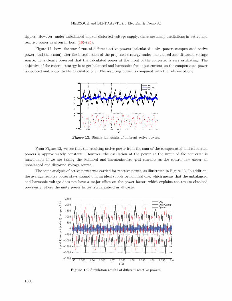
The same analysis of active power was carried for reactive power, as illustrated in Figure 13. In addition,
the average reactive power stays around 0 in an ideal supply or nonideal one, which means that the unbalanced
and harmonic voltage does not have a major effect on the power factor, which explains the results obtained
previously, where the unity power factor is guaranteed in all cases.
1.55 1.555 1.56 1.565 1.57 1.575 1.58 1.585 1.59 1.595 1.6−2500
−2000
−1500
−1000
−500
0
500
1000
1500
2000
2500
t (s)
Q cal, Q
comp, Q
cal + Q comp (VAR) Qcal
Qcal+QcompQcomp
Figure 13. Simulation results of different reactive powers.
1860

MERZOUK and BENDAAS/Turk J Elec Eng & Comp Sci
Figure 14 shows the frequency spectra of active and reactive powers demonstrated by black color in
Figures 12 and 13. It is observed that the 2nd and the 6th harmonics still exist in instantaneous powers.
This is consistent with the theoretical derivation in Section 2. After applying the proposed control target,
I−α=I−β =I5α=I5β= 0, the active and reactive powers are given by Eqs. (26) and (27). The interaction between
the negative sequence of the voltage and the fundamental of the current generates the 2nd harmonic in active
and reactive powers, and the interaction of the 5th sequence of voltage with the fundamental of current generates
the 6th harmonic in active and reactive powers.
0 50 100 150 200 250 300 350 400 450 250 300 350 400 4500
1000
2000
3000
4000
5000
6000
Frequency (Hz)
a
Mag
0 50 100 150 2000
200
400
600
800
1000
1200
1400
Frequency (Hz)
b
Mag
Figure 14. Frequency spectra of input powers: (a) active power, (b) reactive power.
5. Conclusion
This paper has proposed a modified DPC-SVM strategy for a 3-phase 3-level neutral point clamped converter
supplied by an unbalanced and/or harmonically polluted voltage source. In order to obtain balanced and
sinusoidal grid currents under unbalanced and/or harmonically polluted voltage conditions, compensated powers
are calculated and added to the original referenced power to achieve balanced and high quality input current.
The positive, negative, and harmonic sequences of the voltage and the current are extracted using the MCCF
filter. The modified strategy is verified by simulation for three cases, which are unbalanced voltage, distorted
voltage, and simultaneously unbalanced and distorted voltage. It proves its capability of yielding sinusoidal and
balanced grid current with unity power factor under a severe nonideal source. The control scheme also took
into consideration the DC-link voltage balance at the output of the converter.
References
[1] Xiao P, Corzine KA, Venayagamoorthy GK. Multiple reference frame-based control of three-phase PWM boost
rectifiers under unbalanced and distorted input conditions. IEEE T Power Electron 2008; 23: 2006-2017.
[2] Busquets-Monge S, Ortega JD, Bordonau J, Beristain JA, Rocabert J. Closed-loop control of a three-phase neutral-
point-clamped inverter using an optimized virtual-vector-based pulsewidth modulation. IEEE T Ind Electron
2008;55: 2061-2071.
[3] Moran L, Ziogas PD, Joos G. Design aspects of synchronous PWM rectifier-inverter systems under unbalanced
input voltage conditions. IEEE T Ind Appl 1992; 28: 1286-1293.
[4] Rioual P, Pouliquen H, Louis JP. Regulation of a PWM rectifier in the unbalanced network using a generalized
model. IEEE T Power Electron 1996;11: 495-502.
[5] Suh YS, Lipo TA. Control scheme in hybrid synchronous stationary frame for PWM AC/DC converter under
generalized unbalanced operating conditions. IEEE T Ind Appl 2006; 42: 825-835.
1861

MERZOUK and BENDAAS/Turk J Elec Eng & Comp Sci
[6] Etxeberria-Outadui I, Viscarret U, Caballero M, Rufer A, Bacha S. New optimized PWM VSC control structures
and strategies under unbalanced voltage transients. IEEE T Ind Electron 2007; 54: 2902-2914.
[7] Hu J, Zhang W, Wang H, He Y, Xu L. Proportional and integral plus multi-frequency resonant current controller
for grid-connected voltage source converter under imbalanced and distorted supply voltage conditions. J Zhejiang
Univ-SCA 2009; 10: 1532-1540.
[8] Alepuz S, Busquets-Monge S, Bordonau J, Martınez-Velasco JA, Silva CA, Pontt J, Rodrıguez J. Control strategies
based on symmetrical components for grid-connected converters under voltage dips. IEEE T Ind Electron 2009; 56:
2162-2173.
[9] Eloy-Garcia J, Arnaltes S, Redriguez-Amenedo JL. Direct power control of voltage source inverters with unbalanced
grid voltages. IET Power Electron 2007; 1: 395-407.
[10] Shang L, Sun D, Hu J. Sliding-mode-based direct power control of grid connected voltage-sourced inverters under
unbalanced network conditions. IET Power Electron 2011; 4: 570-579.
[11] Shang L, Hu J. Sliding-mode-based direct power control of grid-connected wind- turbine-driven doubly fed induction
generators under unbalanced grid voltage conditions. IEEE T Energy Conver 2012; 27: 362-373.
[12] Merzouk I, Bendaas ML, Gaafazi A, Rizaoui M. Improved direct power control for three-level AC/DC converter
under unbalanced voltage source conditions. In: 1st International Conference on Power Electronics and Their
Applications; 6–7 November 2013; Djelfa, Algeria.
[13] Portillo R, Vazquez S, Leon JI, Parts MM, Franquelo LG. Model based adaptive direct power control for three-level
NPC converters. IEEE T Ind Inform 2013; 9: 1148-1157.
[14] Lalili D, Berkouk EM, Boudjema F , Lourci N, Taleb T, Petzold J. Simplified space vector PWM algorithm for
three-level inverter with neutral point potential control. Mediterranean Journal of Measurement and Control 2007;
3: 30-39.
[15] Guo X, Wu W, Chen Z. Multiple-complex coefficient-filter-based phase-locked loop and synchronization technique
for three-phase grid-interfaced converters in distributed utility networks. IEEE T Ind Electron 2011; 58: 1194-1204.
[16] Antoniewicz P. Predictive control of three phase AC/DC converters. PhD, Warsaw University of Technology,
Warsaw, Poland, 2009.
1862

MERZOUK and BENDAAS/Turk J Elec Eng & Comp Sci
Appendix SVM block
A simplified SVM algorithm for a three-level PWM converter is used in this work proposed by [14].
Figure 15 shows the space vector diagram of the 3-level rectifier.
d
q
PNNPOO
ONN
PNO
PON
PNPONP
PPNOPN
PPO
OON
PPP
OOO
NNN
NPN
NPO
NPP
NOP
NNP
OPO
NON
OPP
NOO
OOP
NNO
POP
ONO
Figure 15. Space vector diagram of 3-level converter.
The simplification is made by noting that the space vector diagram of a three-level converter is composed
of six small hexagons that are the space vector diagrams of two-level converters as shown in Figure 16.
2
1
3
4
56
Figure 16. Simplification of a 3-level space vector diagram.
To reach this simplification, two steps have to be done. First, from the location of the given reference
voltage, one hexagon has to be selected among the 6 small hexagons of the 3-level space vector diagram. There
1

MERZOUK and BENDAAS/Turk J Elec Eng & Comp Sci
exist some regions that are overlapped by 2 adjacent small hexagons. These regions will be divided in equality
between the 2 hexagons as shown in Figure 16. Each hexagon is identified by a number S, defined in Table 2.
Table 2. Sector selection.
S 1 2 3 4 5 6θ −π
6 < θ < π6
π6 < θ < π
2π2 < θ < 5π
65π6 < θ < 7π
67π6 < θ < 3π
23π2 < θ < 11π
6
Second, we translate the origin of the reference voltage vector towards the center of the selected hexagon
as indicated in Figure 17. This translation is done by subtracting the center vector of the selected hexagon
from the original reference vector. This translation is done by subtracting the center vector of the selected
hexagon from the original reference vector. Table 3 gives the components d and q of the reference voltage Vs
after translation.
d’
d
q’
q
POO
OON
Vs* ’Vs*
θ
Figure 17. Translation of 3-level reference voltage vector.
Table 3. Correction of three-level vectors.
s 1 2 3 4 5 6
V ∗′sd V ∗
sd − (Vdc/2) V ∗sd − (Vdc/4) V ∗
sd + (Vdc/4) V ∗sd + (Vdc/2) V ∗
sd + (Vdc/4) V ∗sd + (Vdc/4)
V ∗′sq V ∗
sq V ∗sq − (
√3/4)Vdc V ∗
sq − (√3/4)Vdc V ∗
sq V ∗sq + (
√3/4)Vdc V ∗
sq + (√3/4)Vdc
In the space vector diagram of the 3-level rectifier in Figure 15, we can distinguish four types of vectors:
large vectors, medium vectors, small vectors, and zero vectors.
To ensure the voltage balance of the DC-link capacitor we change between positive and negative small
redundant vectors depending on the values of Vdc1 and Vdc2. Taking the example of the first vector, if current
ia >0 and Vdc1-Vdc2 >0, we use the first redundancy (POO) to make the difference equal 0; if Vdc1-Vdc2 <0,
we use the second redundancy (ONN); and the opposite if the current ia <0 and the same philosophy for the
other vectors is illustrated in Table 4.
2

MERZOUK and BENDAAS/Turk J Elec Eng & Comp Sci
Table 4. Selection of redundant voltage vectors.
Redundancy Current Uc1 Uc2 Redundancy Current Uc1 Uc2
V1
A POOi1 >0 + -
V4
A OPPi1 >0 + -
i1 <0 - + i1 <0 - +
B ONNi1 >0 - +
B NOOi1 >0 - +
i1 <0 + - i1 <0 + -
V2
A PPOi3 >0 + -
V5
A OOPi3 >0 + -
i3 <0 - + i3 <0 - +
B OONi3 >0 - +
B NNOi3 >0 - +
i3 <0 + - i3 <0 + -
V3
A OPOi2 >0 + -
V6
A POPi2 >0 + -
i2 <0 - + i2 <0 - +
B NONi2 >0 - +
B ONOi2 >0 - +
i2 <0 + - i2 <0 + -
3


![Efficient features for smartphone-based iris recognitionjournals.tubitak.gov.tr/elektrik/issues/elk-19-27-3/elk-27-3-3-1809-98.pdf · nition. Poornima and Subramanian [22] employed](https://img.pdfslide.us/doc/110x75/5e03ec254100d8748d06cff2/efficient-features-for-smartphone-based-iris-nition-poornima-and-subramanian-22.jpg)