Embed Size (px)
Citation preview
XAPP1290 (v1.3) March 9, 2018 1www.xilinx.com
SummaryThis application note describes a module containing control logic to couple the Xilinx® SMPTE SD/HD/3G-SDI LogiCORE™ IP core with the Kintex® UltraScale™ GTH transceivers to form a complete SDI interface. An example SDI design that runs on the Xilinx KCU105 evaluation board is also provided.
Reference DesignThe Society of Motion Picture and Television Engineers (SMPTE) serial digital interface (SDI) standards are widely used in professional broadcast video equipment. SDI interfaces are used in broadcast studios and video production centers to carry uncompressed digital video, along with embedded ancillary data such as multiple audio channels.
The SMPTE SD/HD/3G-SDI LogiCORE IP core (SDI core) is a generic SDI receive/transmit datapath that does not have any device-specific control functions. It can be connected to a GTH transceiver to implement an SDI interface capable of supporting the SMPTE SD-SDI, HD-SDI and 3G-SDI standards. The SDI core and GTH transceiver must be supplemented with some additional logic to connect them and implement a fully functional SDI interface. This application note describes the additional control and interface logic and a reference design (example SDI design). This document uses the term SDI to refer to the SMPTE interface standards including SD-SDI, HD-SDI and 3G-SDI. Additional information for these interfaces is available from SMPTE [Ref 1].
Kintex UltraScale GTH transceivers can support all SDI bit rates up to, and including, 3G-SDI. The maximum line rates supported by GTH transceivers for each combination of speed grade and device package are described in Kintex UltraScale FPGAs Data Sheet: DC and AC Switching Characteristics (DS892) [Ref 2].
Hardware
The primary functions of the device-specific control logic are:
• Reset logic for GTH transceivers
• Dynamic switching of the RX and TX serial clock dividers to support SD-SDI, HD-SDI and 3G-SDI
Application Note: Kintex UltraScale FPGAs
XAPP1290 (v1.3) March 9, 2018
Implementing SMPTE 3G-SDI Interfaces with Kintex UltraScale GTH TransceiversAuthors: Kalyanchakravathy Podalakuri, S Shreesh
Reference Design
XAPP1290 (v1.3) March 9, 2018 2www.xilinx.com
• Dynamic TX reference clock switching to support two different bit rates in each of the HD-SDI and 3G-SDI standards:
° 1.485 Gb/s and 1.485/1.001 Gb/s in HD-SDI mode
° 2.97 Gb/s and 2.97/1.001 Gb/s in 3G-SDI mode
• Data recovery unit for recovering data in SD-SDI mode
• RX bit-rate detection to determine if the receiver is receiving integer frame-rate signals (line rates such as 1.485 Gb/s and 2.97 Gb/s) or fractional frame-rate signals (line rates such as 1.485/1.001 Gb/s and 2.97/1.001 Gb/s)
To simplify the process of creating an SDI interface, the example SDI design supplies a wrapper file that contains an instance of the control module for the GTH transceiver, one GTH transceiver channel instance, and the SDI core with the necessary connections between them.
The IP cores and modules used in the example SDI design are listed here. Xilinx IP cores are available in the Vivado Design Suite IP catalog:
• The SDI core refers to the SMPTE SD/HD/3G-SDI LogiCORE IP that is available in the Vivado IP catalog. The SDI core implements SMPTE SD-SDI, HD-SDI and 3G-SDI standards. See the SMPTE SMPTE SD/HD/3G-SDI 3.0 LogiCORE IP Product Guide (PG071) [Ref 3] for reference information.
• The control module implements the various device-specific functions required when using the GTH transceiver and the SDI core to implement an SDI interface. The control module is supplied as source code with the example SDI design.
• The UltraScale FPGAs Transceivers Wizard IP core generates a GTH transceiver wrapper that includes an instance of a single GTHE3_CHANNEL primitive and a corresponding control module. See UltraScale FPGAs Transceivers Wizard LogiCORE IP Product Guide (PG182) [Ref 4] for reference information.
• The SDI wrapper instantiates and interconnects the SDI core, GTH wizard IP core, and the control module. The SDI wrapper is supplied as source code with the example SDI design.
• The SDI wrapper support module contains one SDI wrapper instance and a GTHE3_COMMON primitive for a GTH Quad. This wrapper is instantiated once per Quad. The associated QPLL clock, reference clock, and lock outputs should be connected to the SDI wrapper residing in the same Quad but in a different channel. If the QPLL is not used in the SDI application, this wrapper is not required.
Reference Design
XAPP1290 (v1.3) March 9, 2018 3www.xilinx.com
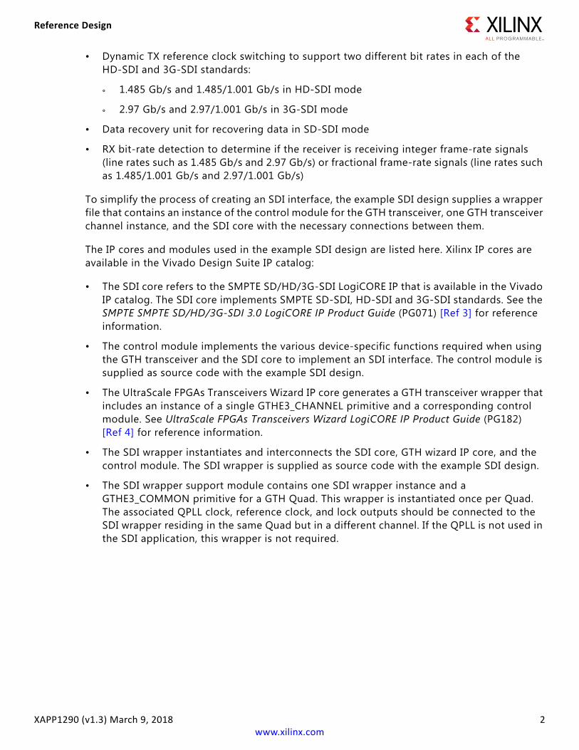
Figure 1 shows a block diagram of a typical SDI interface.
Note: The optional audio embedder shown in Figure 1 is a separate core and is not included with the SDI core or with the example SDI design.
Features
Refer to the SMPTE SD/HD/3G-SDI 3.0 LogiCORE IP Product Guide (PG071) [Ref 3] for reference information including descriptions of the SDI core features, supported SMPTE standards, and timing diagrams of the core in the various SDI modes.
This document uses the term elementary data streams to refer to an SDI data stream that is not multiplexed. For example, an HD-SDI signal consists of two elementary data streams, usually referred to as the Y and C data streams, that are multiplexed onto the virtual 10-bit HD-SDI interface. Likewise, a 3G-SDI level A signal also consists of two elementary data streams, called data stream 1 and data stream 2, that are multiplexed onto the 10-bit virtual 3G-SDI interface. A 3G-SDI level B signal, however, consists of four elementary data streams, a Y and a C data stream for each of the HD-SDI signals that are aggregated together onto the 3G-SDI level B
X-Ref Target - Figure 1
Figure 1: Block Diagram of a Typical SDI Interface
Audio Embedder(Optional)
SDI Wrapper
SMPTE SDI Core
Control Module
40
32
2
2
GTH Wizard IP
20
20
GTH Common
Reference Clock Source
Cable Driver
EQ
Cable Equalizer
SDI Wrapper Support
40
40
40
32
Reference Design
XAPP1290 (v1.3) March 9, 2018 4www.xilinx.com
interface. These four elementary streams get interleaved in a 4-way multiplex onto the 10-bit virtual 3G-SDI interface.
The SDI core TX only accepts, and the RX only outputs, elementary, non-multiplexed, data streams on its data stream inputs and outputs. Multiplexing and demultiplexing data streams occur internally to the SDI core and requires no consideration outside of the SDI core. SD-SDI is an exception to this. The ST 259 SD-SDI standard defines a single data stream that carries both the Y and C components. This is considered to be an elementary data stream by the SDI core because multiple EAVs and SAVs are not interleaved.
The SDI core does no mapping between native video formats and elementary data streams. The user application must do any necessary mapping of video to elementary data streams prior to providing those streams to the SDI transmitter and must reconstruct the video image from the elementary streams output by the SDI receiver. For all video formats on SD-SDI, single-link HD-SDI, and for 1080p 50 Hz, 1080p 59.94 Hz, and 1080p 60 Hz 4:2:2 YCBCR 10-bit video on 3G-SDI level A, no mapping is necessary because there is a one-to-one correspondence between the data streams of these formats and the elementary data streams into and out of the SDI core. This is also true for 3G-SDI level B-DS, the dual stream mode where two HD-SDI video formats are aggregated onto a single 3G-SDI interface. For dual-link HD-SDI, 3G-SDI level B-DL, mapping of the video formats to and from elementary data streams is required and is not done in the SDI core.
The SDI RX automatically determines how many elementary data streams are present in the incoming SDI signal, demultiplexes the data stream appropriately, and indicates on the rx_active_streams port how many elementary data streams are present in the incoming signal.
Using GTH Transceivers for SDI Interfaces
The information in this section supplements the information in the UltraScale Architecture GTH Transceivers User Guide (UG576) [Ref 5]. This information highlights features and operating requirements of GTH transceivers that are of particular importance for SDI applications.
This document uses same GTH transceiver port naming convention used in [Ref 5] which is to use only the base name of a port. When the UltraScale FPGAs Transceiver Wizard is used to create a GTH Wizard module, all input ports names have a suffix of _in and all outputs have a suffix of _out. For example, when a port named txpllclksel is discussed in this document, the actual name of that port in the GTH wrapper would be txpllclksel_in.
GTH transceiver applications require several clocks. The SDI protocol does not allow for clock correction by stuffing and removing extra data in the data stream. For this reason, how these clocks are generated and used in the application requires careful attention. GTH transceivers also require reference clocks to operate. The reference clocks are used by phase-locked loops (PLLs) in the GTH Quad to generate serial clocks for the receiver and transmitter sections of each transceiver. As described in GTH Transceiver Reference Clocks, the serial bit rate of the GTH transmitter is an integer multiple of the reference clock frequency it is using. Also, the data rate of the video provided to the input of the SDI transmitter datapath must exactly match (or be a specific multiple of) the frequency of the reference clock used by the GTH transmitter. Consequently, you must determine how to generate the transmitter reference clock so that it is frequency-locked exactly with the data rate of the video stream being transmitted.
Reference Design
XAPP1290 (v1.3) March 9, 2018 5www.xilinx.com
GTH transmitter clocking is handled by the transmitter user clocking network helper block when enabled during GTH IP core generation from the UltraScale FPGAs Transceiver Wizard. The txusrclk and txusrclk2 output is driven by a BUFG_GT within the helper block and its frequency is exactly equal to the word rate of the data that must enter the txdata port of the GTH transmitter. The txusrclk and txusrclk2 are generated in the GTH transmitter by dividing the serial clock from the PLL down to the word rate. See UltraScale FPGAs Transceivers Wizard LogiCORE IP Product Guide (PG182) [Ref 4] for reference information on the transmitter user clocking network helper block.
The GTH receiver reference clock does not need an exact relationship with the bit rate of the incoming SDI signals. This is because the clock and data recovery (CDR) unit in the GTH receiver can receive bit rates that are up to ±1,250 ppm (<6.6 Gb/s) or ±200 ppm (> 8.0 Gb/s) away from the nominal bit rate as set by the reference clock frequency. This allows the receiver reference clock to be generated by local oscillators that have no exact frequency relationship to the incoming SDI signal. The GTH receiver generates a recovered clock that is frequency-locked to the incoming SDI bit rate. These clocks are output as rxusrclk and rxusrclk2 ports of the receiver user clocking network helper block from the GTH wizard IP and are driven by BUFG_GT. As is described in more detail later in this application note, rxusrclk and rxusrclk2 are true recovered clocks when receiving all SDI line rates except when receiving SD-SDI signals.
One additional clock is required for SDI applications. This is a free-running, fixed-frequency clock that is used as the clock for the dynamic reconfiguration port (DRP) of the GTH transceiver. This same clock is also usually supplied to the control module in the SDI wrapper where it is used for timing purposes. The valid frequency range for this clock is stated in UltraScale FPGAs Transceivers Wizard LogiCORE IP Product Guide (PG182) [Ref 4] and normally ranges from 3.125 to 200 MHz. The frequency of this clock does not require any specific relationship relative to other clocks or data rates of the SDI application. This clock must not change frequencies when the SDI mode changes. It must always remain running at the same nominal frequency at all times. It also must never stop while the SDI application is active. This clock can be used for all SDI interfaces in the device.
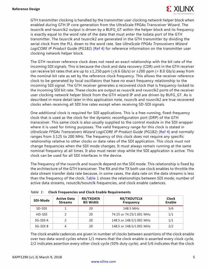
The frequency of the rxusrclk and txusrclk depend on the SDI mode. This relationship is fixed by the architecture of the GTH transceiver. The RX and the TX both use clock enables to throttle the data stream transfer data rate because, in some cases, the data rate on the data streams is less than the frequency of the clock. Table 1 shows the relationships between SDI mode, number of active data streams, rxoutclk/txoutclk frequencies, and clock enable cadences.
The clock enable cadences are given in number of clocks between assertions of the clock enable over two data-word cycles where 1/1 means that the clock enable is asserted every clock cycle, 2/2 indicates assertion every other clock cycle (50% duty cycle), and 5/6 indicates that the clock
Table 1: Clock Frequencies and Clock Enable Requirements
SDI-ModeActive Data
StreamsRX/TXDATABit Width
RX/TXOUTCLKFrequency
ClockEnable
SD-SDI 1 20 148.5 MHz 5/6
HD-SDI 2 20 74.25 or 74.25/1.001 MHz 1/1
3G-SDI A 2 20 148.5 or 148.5/1.001 MHz 1/1
3G-SDI B 4 20 148.5 or 148.5/1.001 MHz 2/2
Reference Design
XAPP1290 (v1.3) March 9, 2018 6www.xilinx.com
enable alternates between assertion every 5 or 6 clock cycles, to average once every 5.5 clock cycles (one instance of 5 clock cycles between logic High pulses on the clock enabled followed by one instance of 6 clock cycles between logic High pulses on the clock enable, with this pattern repeating).
GTH Transceiver Reference Clocks
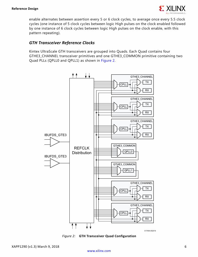
Kintex UltraScale GTH transceivers are grouped into Quads. Each Quad contains four GTHE3_CHANNEL transceiver primitives and one GTHE3_COMMON primitive containing two Quad PLLs (QPLL0 and QPLL1) as shown in Figure 2.
X-Ref Target - Figure 2
Figure 2: GTH Transceiver Quad Configuration
IBUFDS_GTE3
IBUFDS_GTE3
Reference Design
XAPP1290 (v1.3) March 9, 2018 7www.xilinx.com
The clock generated by the QPLL0 and QPLL1 are distributed to all four transceivers in the Quad. Each GTHE3_CHANNEL has its own PLL called the Channel PLL (CPLL), which can provide a clock to the RX and TX of that transceiver only. Each RX and TX unit in the Quad can be individually configured to use either or both QPLL0 or/and QPLL1 or the CPLL as its clock source. Furthermore, any RX or TX unit can dynamically switch its clock source between QPLL0, QPLL1 and CPLL. This configuration and the dynamic switching capability are particularly useful for SDI applications.
Typical SDI applications require the GTH transceivers to support five different bit rates:
• 270 Mb/s for SD-SDI
• 1.485 Gb/s for HD-SDI
• 1.485/1.001 Gb/s for HD-SDI
• 2.97 Gb/s for 3G-SDI
• 2.97/1.001 Gb/s for 3G-SDI
The CDR unit in the RX section of the GTH transceiver can support receiving bit rates that are up to ±1,250 ppm from the reference frequency at bit rates less than 6.6 Gb/s. HD-SDI and 3G-SDI have two bit rates that differ by exactly 1,000 ppm. For HD-SDI and 3G-SDI, both bit rates can be received using a single reference clock frequency. That same reference clock frequency can also support reception of SD-SDI. Thus, for all SDI modes, just a single RX reference clock frequency is required.
The source of the GTH transceiver reference clocks is very application specific. The receiver reference clock source can be a local oscillator because it does not need to match the incoming SDI bit rate exactly. However, because the GTH transmitter line rate is always an integer multiple of the reference clock frequency, the frequency of the transmitter reference clock must be exactly related to the data rate of the transmitted data. Most often, the transmitter reference clocks are generated by genlock PLLs, thereby deriving the GTH transmitter line rate from the studio video reference signal. In some cases, such as the SDI pass-through connection, the transmitter line rate is derived from the recovered clock of the GTH receiver that is receiving the SDI signal. In such cases, an external PLL is required to reduce the jitter on the recovered clock before using it as the transmitter reference clock.
In a typical SDI application, the two reference clocks are connected to the QPLL0 and QPLL1. The RX and TX units of each transceiver in the Quad dynamically switch between the PLL clocks, depending on the bit rate that is required at the moment. The GTH txsysclksel and rxsysclksel ports are used to select the TX and RX units serial clock source between the PLLs. This common configuration for SDI applications is shown in Figure 3. In this figure, multiplexers that are not used dynamically in the implementation have been replaced with wires and the reference clock routing between Quads is not shown.
Therefore, most SDI applications provide two separate reference clocks to the GTH Quad. Usually, the supplied reference frequency pair are 148.5 MHz and 148.5/1.001 MHz or 74.25 MHz and 74.25/1.001 MHz.
Reference Design
XAPP1290 (v1.3) March 9, 2018 8www.xilinx.com
IMPORTANT: This application note always refers to the reference clock frequency pair 148.5 MHz and 148.5/1.001 MHz. However, the alternative reference clock frequency pair of 74.25 MHz and 74.25/1.001 MHz, even though not specifically mentioned, is supported.
Each GTH RX and TX unit has a serial clock divider that divides the selected clock by several selectable integer powers of two. This allows all of the RX units in the Quad to use the same clock frequency from the QPLL but operate at different lines rates by using different serial clock divider values. This is useful for SDI interfaces because the 3G-SDI bit rate is exactly twice as fast the HD-SDI bit rate. For 270 Mb/s SD-SDI, the GTH transceiver runs at the 3G-SDI line rate using 11X oversampling techniques. The ability of the RX and TX units to locally divide the clock source by four divisors that differ by a factor of two is important, allowing reception and transmission of all SDI bit rates using just two reference clock frequencies.
The serial clock divider value of each RX and TX unit can be changed dynamically through the DRP, by using the RXOUT_DIV and TXOUT_DIV attributes.
X-Ref Target - Figure 3
Figure 3: Typical GTH Reference Clock Implementation for SDI
Reference Design
XAPP1290 (v1.3) March 9, 2018 9www.xilinx.com
The configuration shown in Figure 3 is an optimal solution for most SDI applications for several reasons:
• The receivers can receive all SDI bit rates when using QPLL0 and QPLL1 to provide the serial clock derived from that reference clocks to all receivers in the Quad.
• The transmitters have the flexibility to dynamically switch between the clocks from QPLL0 and QPLL1 to get both frequencies they need to transmit all supported SDI bit rates.
• All four receivers and all four transmitters in the Quad are fully independent and can each be running at different SDI bit rates and can dynamically switch between bit rates without disrupting the other RX or TX units.
• For genlocked applications, modern genlock PLLs usually can simultaneously provide both required reference clock frequencies from the synchronization reference input signal.
In some SDI applications, it might be necessary for different transmitters to be running at slightly different bit rates even though they are transmitting at the same nominal bit rate. This is often the case with SDI routers where the bit rate of each TX must exactly match the bit rate of the SDI signal received by the SDI RX to which the TX is currently connected. In these cases, two transmitters that are transmitting at the same nominal bit rate have bit rates that differ by a few ppm. Supporting such applications is possible with the Kintex UltraScale GTH Quad architecture because each TX unit has exclusive use of its own CPLL. But to accomplish this, each CPLL must be provided with its own individual reference clock frequency, and the number of GTH reference clock inputs is limited. There are two reference clock inputs per GTH Quad. A Quad can use reference clocks from the Quad above and the Quad below. Thus, it is possible to provide some GTH Quads in the device with five different reference clock frequencies (one for the RX and four for the four TX units), but overall, there are obviously not enough reference clock inputs to allow every GTH TX in the device to have its own reference clock. The PICXO technique can be very useful in these cases because it allows a GTH TX to be pulled by a few hundred ppm away from the frequency of its serial clock. Thus, applications where the bit rate of each SDI TX needs to be individually locked to the bit rate of the received SDI signal can be implemented by using common reference clocks as in Figure 3 and then using the PICXO technique with each GTH TX to set the exact bit rate of each SDI transmitter individually. This application note does not cover the PICXO technique. For further information about using PICXO, contact Xilinx technical support.
Resets
The GTH transceiver has very specific reset requirements as described in the UltraScale Architecture GTH Transceivers User Guide (UG576) [Ref 5]. The GTH transceiver requires careful coordination of resets of the PLLs, GTH transceiver resets (gttxreset and gtrxreset). Such coordination is simplified when the GTH transceiver is generated using the UltraScale FPGAs Transceivers Wizard with the clocking network and reset controller helper blocks enabled. The reset controller helper block handles the complicated GTH transceiver reset sequence. The control module supplied with the example SDI design handles the reset assertions for all SDI core configuration updates to ensure proper operation of the GTH transceiver.
Reference Design
XAPP1290 (v1.3) March 9, 2018 10www.xilinx.com
GTH TX Resets
The UltraScale FPGAs Transceiver Wizard offers three ways to reset the TX portion of the GTH transceiver.
• gtwiz_reset_all_in: Asserted logic High. User signal to reset the TX portion and RX portion phase-locked loops (PLLs) and the active data direction of the GTH transceiver. This reset is normally asserted during startup condition.
• gtwiz_reset_tx_pll_and_datapath_in: Asserted logic High. User signal to reset the TX data direction and associated PLLs of GTH transceiver. This reset is particularly useful if the reference clock to the TX PLL changes.
• gtwiz_reset_tx_datapath_in: Asserted logic High. User signal to reset the TX data direction of transceiver primitives. This reset is asserted for SDI TX applications when at least one of the tx_mode, tx_m and tx_mux_pattern ports change.
For applications that use one QPLL and one CPLL, these two PLL types have different operating frequency ranges. For SDI applications, the serial clocks from the QPLLs are twice the frequency of the serial clock from the CPLL. Thus, when the tx_m input port of the SDI wrapper changes to request a dynamic switch of the GTH TX between the two PLLs, a dynamic change of the serial clock divider through the TXOUT_DIV DRP attribute must also be done at the same time if the transmitter is staying in the same SDI mode. For example, when switching from an HD-SDI bit rate of 1.485 Gb/s using the QPLL as the serial clock source to an HD-SDI bit rate of 1.485/1.001 Gb/s using the CPLL as the serial clock source, both the txsysclksel port and TXOUT_DIV DRP attribute must be changed. However, if the SDI mode, as selected by the tx_mode input port of the SDI wrapper, changes at the same time as the tx_m port, the serial clock divider may or may need to be changed. For example, if changing from HD-SDI mode using the CPLL to the 3G-SDI mode using the QPLL, the txrate port does not need to change because changing from the CPLL to the QPLL inherently increases the serial clock frequency and the resulting line rate by a factor of two.
Because tx_mode and tx_m are separate input ports to the SDI wrapper, when one of these ports changes, a small settling delay is implemented before the txsysclksel port, TXOUT_DIV DRP attribute is dynamically changed. This settling delay allows a short window of time for the other port to also change before the TX control logic decides whether these port and DRP attributes need to change.
The SDI wrapper has two reset inputs for the TX section:
• tx_rst_in: When asserted logic High, this input resets the SDI TX data path in the SDI core, TX controller module and TX portion of GTH transceiver
• gth_wiz_reset_tx_pll_and_datapath_in: When asserted logic High, this input resets both the PLL associated with the TX and then the TX section of the GTH transceiver
GTH RX Resets
As with GTH TX resets discussed in GTH TX Resets, an application should rely on the SDI control module to carefully coordinate all of the RX reset and dynamic change activities described here in order to prevent them from interfering with each other.
Reference Design
XAPP1290 (v1.3) March 9, 2018 11www.xilinx.com
The UltraScale FPGAs Transceiver Wizard offers three ways to reset the RX portion of the GTH Transciever.
• gtwiz_reset_all_in: Asserted logic High. User signal to reset the TX portion and RX portion phase-locked loops (PLLs) and the active data direction of the GTH transceiver. This reset is normally asserted during startup condition.
• gtwiz_reset_rx_pll_and_datapath_in: Asserted logic High. User signal to reset the RX data direction and associated PLLs of GTH transceiver. This reset is particularly useful if the reference clock to the RX PLL changes.
• gtwiz_reset_rx_datapath_in: Asserted logic High. User signal to reset the RX data direction of transceiver primitives. This reset is asserted for SDI RX applications when at least one of the tx_mode, rx_m and rx_mux_pattern ports change.
All bit rates (0 ppm and 1,000 ppm) from SD-SDI to 3G-SDI can be supported by one CPLL or QPLL since these PLLs offer ±1,250 ppm for bit rates <6.6 Gb/s.
Changes in the SDI mode between SD-SDI, HD-SDI and 3G-SDI require changes to one or more of the following four items:
• The rxcdrhold port
• Enabling or disabling equalization (LPM and DFE)
• The RXCDR_CFG attribute
• RXOUT_DIV attributes
The RXCDR_CFG2 and RXOUT_DIV attributes are changed through the DRP. The rxcdrhold port must be asserted logic High when the RX SDI mode is SD-SDI. The LPM and DFE must be disabled for SD-SDI and enabled for other SDI line rates. The RXCDR_CFG2 attribute is modified when switching into HD-SDI and 3G-SDI modes to optimize the CDR for the current line rate. The RXOUT_DIV attribute control the serial clock divider for the GTH RX. The GTH RX must be reset using the gtwiz_reset_rx_datapath_in port of GTH wizard IP after dynamic changes are made to any of these four items. If more than one of these item changes during the same SDI mode change sequence, only a single gtwiz_reset_rx_datapath_in is required after all changes have been made.
The SDI wrapper has two reset inputs for the RX section:
• rx_rst_in: When asserted logic High, this input resets the SDI RX data path in the SDI core, RX controller module and RX portion of GTH transceiver
• gth_wiz_reset_rx_pll_and_datapath_in: When asserted logic High, this input resets both the PLL associated with the RX and then the RX section of the GTH transceiver
GTH PLL Usage Models for SDI Applications
This section describes several typical configurations of PLLs and transceivers used in SDI applications. Not every possible configuration is described, but the configurations shown here are sufficient to describe the proper connection of the PLL reset and locked signals.
Reference Design
XAPP1290 (v1.3) March 9, 2018 12www.xilinx.com
The SDI wrapper has four static parameters that specify which serial clock sources come from the QPLLs and which come from the CPLL. These attributes do not control the routing of PLL clocks. They are only used to calculate the correct RX and TX serial clock divider values and, for the TX, the value to drive onto the GTH wizard IP rxpllclksel_in and txpllclksel_in ports based on the current value of rx_m and tx_m respectively. These four parameters are two bit binary values and must be assigned values as described here:
• The RXPLLCLKSEL_RX_M_0 parameter must be set to 2'b00 (CPLL) or 2'b11 (QPLL0) or 2'b10 (QPLL1) depending on the clock source for the GTH RX when rx_m is logic Low.
• The RXPLLCLKSEL_RX_M_1 parameter must be set to 2'b00 (CPLL) or 2'b11 (QPLL0) or 2'b10 (QPLL1). For this Application note and reference design, this parameter is not used. The value for this parameter can be set same as RXPLLCLKSEL_RX_M_0.
• The TXPLLCLKSEL_TX_M_0 parameter must be set to 2'b00 (CPLL) or 2'b11 (QPLL0) or 2'b10 (QPLL1) depending on the clock source for the GTH TX when tx_m is logic Low.
• The TXPLLCLKSEL_TX_M_1 parameter must be set to 2'b00 (CPLL) or 2'b11 (QPLL0) or 2'b10 (QPLL1) depending on the clock source for the GTH TX when tx_m is logic High.
There are two parameters for the TX clock to support dynamic switching of the TX between the two PLL clock sources using the tx_m port of the SDI wrapper. TXPLLCLKSEL_TX_M_0 is used to drive the txpllclksel_in when tx_m is logic Low and TXPLLCLKSEL_TX_M_1 is used when tx_m is logic High. In applications where the TX PLL is not dynamically switched, set the same value for both TXPLLCLKSEL_TX_M_0 and TXPLLCLKSEL_TX_M_1 depending on clock source to TX PLL.
Usage Model One
Usage model one consists of a single transceiver active in the Quad, RX is clocked by QPLL1 and TX is dynamically clocked by QPLL1 and CPLL.
In this usage model, only one QPLL is used. Both bit rates for 3G-SDI and lower line rates are supported by TX and RX. Since TX can switch between QPLL1 and CPLL. RX uses QPLL1 which has ±1,250 ppm tolerance for bit rates <6.6 Gb/s. Usage model one is shown in Figure 4.
Reference Design
XAPP1290 (v1.3) March 9, 2018 13www.xilinx.com
These connections must be made:
• Connect one reference clock to the gth_qpll1_refclk_p_in and gth_qpll1_refclk_n_in ports
• Connect one reference clock to the gth_cpll_refclk_p_in and gth_cpll_refclk_n_in ports
• The gth_qpll0_refclk_p_in and gth_qpll0_refclk_n_in ports must be connected to logic Low
• The gth_drpclk_in must be connected to clock specified during GTH Wizard IP generation, in this application note it is 27 MHz
• The gth_wiz_reset_tx_pll_and_datapath_in input port must be logic Low only when the reference clock source to the QPLL1 and CPLL are stable
• The gth_wiz_reset_rx_pll_and_datapath_in input port must be logic Low only when the reference clock source to the QPLL1 is stable
• The RXPLLCLKSEL_RX_M_0 parameter of the SDI wrapper support must be set to 2'b10 (QPLL1)
• The RXPLLCLKSEL_RX_M_1 parameter of the SDI wrapper support must be set to 2'b10 (QPLL1)
• The TXPLLCLKSEL_TX_M_0 parameter of the SDI wrapper support must be set to either 2'b10 (QPLL1) or 2'b00 (CPLL)
• The TXPLLCLKSEL_TX_M_1 parameter of the SDI wrapper support must be set to either 2'b00 (CPLL) or 2'b10 (QPLL1) depending on the reference clock connection and which is not used on TXPLLCLKSEL_TX_M_0
X-Ref Target - Figure 4
Figure 4: PLL Usage Model One and Two
Reference Design
XAPP1290 (v1.3) March 9, 2018 14www.xilinx.com
• When the QPLL1 needs to be reset due to a reference clock change or interruption, assert the gth_qpll1_reset_in input of the SDI wrapper support
Note: The usage model can also use QPLL0 instead of QPLL1. In this case parameter should be set to 2'b11 (QPLL0). Reference clock ports should be connected accordingly.
Usage Model Two
Usage model two consists of a single transceiver active in the Quad, RX is clocked by CPLL and TX is dynamically clocked by QPLL1 and CPLL.
In this usage model, only one QPLL is used. Both bit rates for 3G-SDI and lower line rates are supported by TX and RX. Since TX can switch between QPLL1 and CPLL. RX uses CPLL which has ±1250 ppm tolerance for bit rates <6.6 Gb/s. Usage model two is shown in Figure 4.
These connections must be made:
• Connect one reference clock to the gth_qpll1_refclk_p_in and gth_qpll1_refclk_n_in ports
• Connect one reference clock to the gth_cpll_refclk_p_in and gth_cpll_refclk_n_in ports
• The gth_qpll0_refclk_p_in and gth_qpll0_refclk_n_in ports must be connected to logic Low
• The gth_drpclk_in must be connected to clock specified during GTH Wizard IP generation, in this application note it is 27 MHz
• The gth_wiz_reset_tx_pll_and_datapath_in input port must be logic Low only when the reference clock source to the QPLL1 and CPLL are stable
• The gth_wiz_reset_rx_pll_and_datapath_in input port must be logic Low only when the reference clock source to the QPLL1 is stable
• The RXPLLCLKSEL_RX_M_0 parameter of the SDI wrapper support must be set to 2'b00 (CPLL)
• The RXPLLCLKSEL_RX_M_1 parameter of the SDI wrapper support must be set to 2'b00 (CPLL).
• The TXPLLCLKSEL_TX_M_0 parameter of the SDI wrapper support must be set to either 2'b10 (QPLL1) or 2'b00 (CPLL)
• The TXPLLCLKSEL_TX_M_1 parameter of the SDI wrapper support must be set to either 2'b00 (CPLL) or 2'b10 (QPLL1) depending on the reference clock connection and which is not used on TXPLLCLKSEL_TX_M_0
• When the QPLL1 needs to be reset due to a reference clock change or interruption, assert the gth_qpll1_reset_in input of the SDI wrapper support.
Note: The usage model can also use QPLL0 instead of QPLL1. In this case parameter should be set to 2'b11 (QPLL0). Reference clock ports should be connected accordingly.
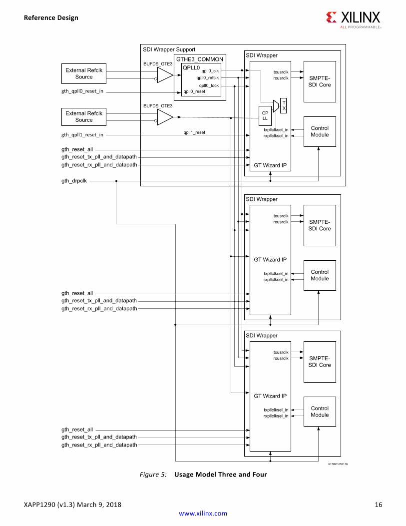
Usage Model Three
Usage model three consists of multiple transceivers active in a Quad, all RX is clocked by QPLL1 and all TX is dynamically clocked by QPLL1 and CPLL.
Reference Design
XAPP1290 (v1.3) March 9, 2018 15www.xilinx.com
In this usage model, there are multiple transceivers active in the Quad. All of the receivers are clocked by the QPLL1. Each transmitter is dynamically clocked by QPLL1 and CPLL. Usage model three is shown in Figure 5.
These connections must be made:
• Connect the reference clocks, to the gth_qpll0_refclk_p/n_in and gth_qpll1_refclk_p/n_in ports
• The gth_cpll_refclk_p_in and gth_cpll_refclk_n_in ports must be connected to logic Low
• The gth_drpclk_in must be connected to clock specified during GTH Wizard IP generation, in the example SDI design it is 27 MHz
• The gth_wiz_reset_tx_pll_and_datapath_in input port must be logic Low only when the reference clock source to the QPLL1 and CPLL are stable
• The gth_wiz_reset_rx_pll_and_datapath_in input port must be logic Low only when the reference clock source to the QPLL1 is stable
• The RXPLLCLKSEL_RX_M_0 parameter of the SDI wrapper support and SDI wrapper must be set to 2'b10 (QPLL1)
• The RXPLLCLKSEL_RX_M_1 parameter of the SDI wrapper support and SDI wrapper must be set to 2'b10 (QPLL1)
• The TXPLLCLKSEL_TX_M_0 parameter of the SDI wrapper support and SDI wrapper must be set to either 2'b10 (QPLL1) or 2'b00 (CPLL)
• The TXPLLCLKSEL_TX_M_1 parameter of the SDI wrapper support and SDI wrapper must be set to either 2'b10 (QPLL1) or 2'b00 (CPLL)
• When the QPLL1 needs to be reset due to a reference clock change or interruption, assert the gth_qpll1_reset_in input of the SDI wrapper support
The SDI wrapper support qpll0/1_clk, qpll0/1_refclk and qpll0/1_lock output ports must be connected to their corresponding ports in the SDI wrapper
Note: The usage model can also use QPLL0 instead of QPLL1. In this case parameter should be set to 2'b11 (QPLL0). Reference clock ports should be connected accordingly.
Reference Design
XAPP1290 (v1.3) March 9, 2018 16www.xilinx.com
X-Ref Target - Figure 5
Figure 5: Usage Model Three and Four
External Refclk Source qpll0_refclk
qpll0_lock
SDI Wrapper
qpll0_clkQPLL0
qpll0_reset
External Refclk Source
IBUFDS_GTE3
qpll1_reset
GT Wizard IP
SMPTE-SDI Core
Control Module
txusrclkrxusrclk
gth_reset_allgth_reset_tx_pll_and_datapathgth_reset_rx_pll_and_datapath
gth_drpclk
SDI Wrapper Support
gth_qpll0_reset_in
gth_qpll1_reset_in txpllclksel_inrxpllclksel_in
SDI Wrapper
GT Wizard IP
SMPTE-SDI Core
Control Module
txusrclkrxusrclk
gth_reset_allgth_reset_tx_pll_and_datapathgth_reset_rx_pll_and_datapath
txpllclksel_inrxpllclksel_in
SDI Wrapper
GT Wizard IP
SMPTE-SDI Core
Control Module
txusrclkrxusrclk
gth_reset_allgth_reset_tx_pll_and_datapathgth_reset_rx_pll_and_datapath
txpllclksel_inrxpllclksel_in
IBUFDS_GTE3GTHE3_COMMON
CPLL
TX
Reference Design
XAPP1290 (v1.3) March 9, 2018 17www.xilinx.com
Usage Model Four
Usage model four consists of multiple transceivers active in a Quad, all RX are clocked by CPLL and all TX are dynamically clocked by QPLL1 and CPLL.
In this usage model, multiple transceivers are active in the Quad. All receivers are clocked by the QPLL1. Each transmitter is dynamically clocked by QPLL1 and CPLL. Usage model four is shown in Figure 5.
These connections must be made:
• Connect the reference clocks, to the gth_qpll0_refclk_p/n_in and gth_qpll1_refclk_p/n_in ports
• The gth_cpll_refclk_p_in and gth_cpll_refclk_n_in ports must be connected to logic low
• The gth_drpclk_in must be connected to clock specified during GTH Wizard IP generation, in the example SDI design it is 27 MHz
• The gth_wiz_reset_tx_pll_and_datapath_in input port must be logic Low only when the reference clock source to the CPLL is stable
• The gth_wiz_reset_rx_pll_and_datapath_in input port must be logic Low only when the reference clock source to the QPLL1 is stable
• The RXPLLCLKSEL_RX_M_0 parameter of the SDI wrapper support and SDI wrapper must be set to 2'b00 (CPLL)
• The RXPLLCLKSEL_RX_M_1 parameter of the SDI wrapper support and SDI wrapper must be set to 2'b00 (CPLL)
• The TXPLLCLKSEL_TX_M_0 parameter of the SDI wrapper support and SDI wrapper must be set to either 2'b10 (QPLL1) or 2'b00 (CPLL)
• The TXPLLCLKSEL_TX_M_1 parameter of the SDI wrapper support and SDI wrapper must be set to either 2'b10 (QPLL1) or 2'b00 (CPLL)
• When the QPLL1 needs to be reset due to a reference clock change or interruption, assert the gth_qpll1_reset_in input of the SDI wrapper support
Note: The usage model can also use QPLL0 instead of QPLL1. In this case parameter should be set to 2'b11 (QPLL0). Reference clock ports should be connected accordingly.
Usage Model Five
Usage model five consists of a single transceiver active in the Quad, RX is clocked by QPLL1 and TX is dynamically clocked by QPLL0 and QPLL1.
Usage model five uses two QPLLs. Bit rates for 3G-SDI and lower line rates are supported by TX and RX. TX can switch between QPLL0 and QPLL1. RX uses QPLL1 which has ±1,250 pm tolerance for bit rates <6.6 Gb/s. Usage model five is shown in Figure 3 and Figure 6.
Reference Design
XAPP1290 (v1.3) March 9, 2018 18www.xilinx.com
These connections must be made:
• Connect one reference clock to the gth_qpll1_refclk_p_in and gth_qpll1_refclk_n_in ports
• Connect one reference clock to the gth_qpll0_refclk_p_in and gth_qpll0_refclk_n_in ports
• The gth_drpclk_in must be connected to clock specified during GTH Wizard IP generation, in the example SDI design it is 27 MHz
• The gth_wiz_reset_tx_pll_and_datapath_in input port must be logic Low only when the reference clock source to the QPLL0 and QPLL1 are stable
• The gth_wiz_reset_rx_pll_and_datapath_in input port must be logic Low only when the reference clock source to the QPLL1 is stable
• The RXPLLCLKSEL_RX_M_0 parameter of the SDI wrapper support must be set to 2'b10 (QPLL1)
• The RXPLLCLKSEL_RX_M_1 parameter of the SDI wrapper support must be set to 2'b10 (QPLL1)
• The TXPLLCLKSEL_TX_M_0 parameter of the SDI wrapper support must be set to either 2'b10 (QPLL1) or 2'b11 (QPLL0)
• The TXPLLCLKSEL_TX_M_1 parameter of the SDI wrapper support must be set to either 2'b11 (QPLL0) or 2'b10 (QPLL1) depending on the reference clock connection and which is not used on TXPLLCLKSEL_TX_M_0
• When the QPLL1 needs to be reset due to a reference clock change or interruption, assert the gth_qpll1_reset_in input of the SDI wrapper support.
X-Ref Target - Figure 6
Figure 6: Usage Model Five
Reference Design
XAPP1290 (v1.3) March 9, 2018 19www.xilinx.com
• When the QPLL0 needs to be reset due to a reference clock change or interruption, assert the gth_qpll0_reset_in input of the SDI wrapper support
SDI Electrical Interface
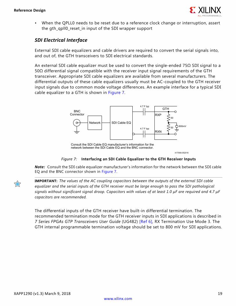
External SDI cable equalizers and cable drivers are required to convert the serial signals into, and out of, the GTH transceivers to SDI electrical standards.
An external SDI cable equalizer must be used to convert the single-ended 75Ω SDI signal to a 50Ω differential signal compatible with the receiver input signal requirements of the GTH transceiver. Appropriate SDI cable equalizers are available from several manufacturers. The differential outputs of these cable equalizers usually must be AC-coupled to the GTH receiver input signals due to common mode voltage differences. An example interface for a typical SDI cable equalizer to a GTH is shown in Figure 7.
Note: Consult the SDI cable equalizer manufacturer's information for the network between the SDI cable EQ and the BNC connector shown in Figure 7.
IMPORTANT: The values of the AC coupling capacitors between the outputs of the external SDI cable equalizer and the serial inputs of the GTH receiver must be large enough to pass the SDI pathological signals without significant signal droop. Capacitors with values of at least 1.0 µF are required and 4.7 µF capacitors are recommended.
The differential inputs of the GTH receiver have built-in differential termination. The recommended termination mode for the GTH receiver inputs in SDI applications is described in 7 Series FPGAs GTP Transceivers User Guide (UG482) [Ref 6], RX Termination Use Mode 3. The GTH internal programmable termination voltage should be set to 800 mV for SDI applications.
X-Ref Target - Figure 7
Figure 7: Interfacing an SDI Cable Equalizer to the GTH Receiver Inputs
4.7 F typ
50
504.7 F typ800mV
Reference Design
XAPP1290 (v1.3) March 9, 2018 20www.xilinx.com
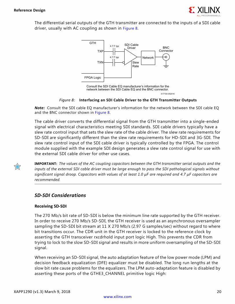
The differential serial outputs of the GTH transmitter are connected to the inputs of a SDI cable driver, usually with AC coupling as shown in Figure 8.
Note: Consult the SDI cable EQ manufacturer's information for the network between the SDI cable EQ and the BNC connector shown in Figure 8.
The cable driver converts the differential signal from the GTH transmitter into a single-ended signal with electrical characteristics meeting SDI standards. SDI cable drivers typically have a slew rate control input that sets the slew rate of the cable driver. The slew rate requirements for SD-SDI are significantly different than the slew rate requirements for HD-SDI and 3G-SDI. The slew rate control input of the SDI cable driver is typically controlled by the FPGA. The control module supplied with the example SDI design generates a slew rate control signal for use with the external SDI cable driver for other use cases.
IMPORTANT: The values of the AC coupling capacitors between the GTH transmitter serial outputs and the inputs of the external SDI cable driver must be large enough to pass the SDI pathological signals without significant signal droop. Capacitors with values of at least 1.0 µF are required and 4.7 µF capacitors are recommended.
SD-SDI Considerations
Receiving SD-SDI
The 270 Mb/s bit rate of SD-SDI is below the minimum line rate supported by the GTH receiver. In order to receive 270 Mb/s SD-SDI, the GTH receiver is used as an asynchronous oversampler sampling the SD-SDI bit stream at 11 X 270 Mb/s (2.97 G samples/sec) without regard to where bit transitions occur. The CDR unit in the GTH receiver is locked to the reference clock by asserting the GTH transceiver rxcdrhold input port logic High. This prevents the CDR from trying to lock to the slow SD-SDI signal and results in more uniform oversampling of the SD-SDI signal.
When receiving an SD-SDI signal, the auto adaptation feature of the low power mode (LPM) and decision feedback equalization (DFE) equalizer must be disabled. The long run lengths at the slow bit rate cause problems for the equalizers. The LPM auto-adaptation feature is disabled by asserting these ports of the GTHE3_CHANNEL primitive logic High:
X-Ref Target - Figure 8
Figure 8: Interfacing an SDI Cable Driver to the GTH Transmitter Outputs
4.7 F typ
4.7 F typ
Reference Design
XAPP1290 (v1.3) March 9, 2018 21www.xilinx.com
• RXLPMGCOVRDEN
• RXLPMHFOVRDEN
• RXLPMLFKLOVRDEN
• RXLPMOSOVRDEN
• RXOSOVRDEN
The DFE equalization is disabled by asserting these ports of the GTHE3_CHANNEL primitive logic High:
• RXDFEAGCOVRDEN
• RXDFELFOVRDEN
• RXDFETAP2OVRDEN
• RXDFETAP3OVRDEN
• RXDFETAP4OVRDEN
• RXDFETAP5OVRDEN
• RXDFETAP6OVRDEN
• RXDFETAP7OVRDEN
• RXDFETAP8OVRDEN
• RXDFETAP9OVRDEN
• RXDFETAP10OVRDEN
• RXDFETAP11OVRDEN
• RXDFETAP12OVRDEN
• RXDFETAP13OVRDEN
• RXDFETAP14OVRDEN
• RXDFETAP15OVRDEN
• RXDFEUTOVRDEN
The UltraScale FPGAs Transceivers Wizard does not enable these ports by default on the GTH Wizard IP and must be manually enabled. These ports are located in the Structural Options tab of the wizard with _in suffixes as port names. Connect the rxcdrhold_in port of the GTH transceiver wrapper to these ports of the GTH Wizard IP. The rxcdrhold_in port is driven logic High by the SDI control logic when the receiver is in SD-SDI mode, so these three ports are driven logic High in SD-SDI mode if connected in this manner.
A data recovery unit (DRU), implemented in the programmable logic of the FPGA, examines the oversampled SD-SDI data from the GTH RX, determines the most likely value for each bit, and outputs the recovered data. This DRU is not part of the SDI core, but is provided as part of the example SDI design SDI control module.
Reference Design
XAPP1290 (v1.3) March 9, 2018 22www.xilinx.com
The DRU provided with the example SDI design is described in Dynamically Programmable DRU for High-Speed Serial I/O (XAPP875) [Ref 7]. This application note describes operation of the DRU, an understanding of operation is not required when using the DRU in the SDI reference design.
The SMPTE SD-SDI standard ST 259 [Ref 1] specifies several bit rates besides 270 Mb/s. The DRU is instantiated into the SDI control module to support only 11X oversampling of 270 Mb/s serial data. If other SD-SDI bit rates must be supported by the application, the DRU can receive other bit rates. Because the DRU supports fractional oversampling, it can receive the other SD-SDI bit rates without requiring additional RX reference clock frequencies. Note that the 540 Mb/s SD-SDI bit rate specified by SMPTE standard ST 344 [Ref 1] is within the supported line rate range of the GTH transceiver. For this reason, the GTH receiver does not require the DRU to receive 540 Mb/s. However, receiving the 540 Mb/s bit rate without the DRU requires a different reference clock frequency than is used for the other SDI bit rates. For this reason, it is convenient to use the DRU to receive the 540 Mb/s ST 344 signal using 5.5X oversampling so that the standard SDI reference clock frequency can be used. The example SDI design does not support additional SD-SDI bit rates.
The DRU does not recover a clock and, because the CDR unit in the GTH receiver is locked to its reference clock, the rxusrclk is not locked to the incoming bit rate in SD-SDI mode. The DRU does produce a data strobe indicating when a 10-bit data word is ready on its output. This data strobe is used by the SDI core to generate a clock enable that is asserted at a 27 MHz rate, typically with a 5/6/5/6 cadence relative to the rxusrclk clock from the GTH Transceiver. The rx_ce_out output of the v_smpte_3gsdi_rxtx wrapper during SD-SDI operations is derived from the DRU data strobe and has the same cadence. Occasionally the cadence of the DRU data strobe and the rx_ce_sd signal will vary from the typical 5/6/5/6 cadence. This occurs when the DRU needs to make up for the slight difference between the actual SD-SDI bit rate and the frequency of the local reference clock provided to the PLL used by the GTH receiver.
Reference Design
XAPP1290 (v1.3) March 9, 2018 23www.xilinx.com
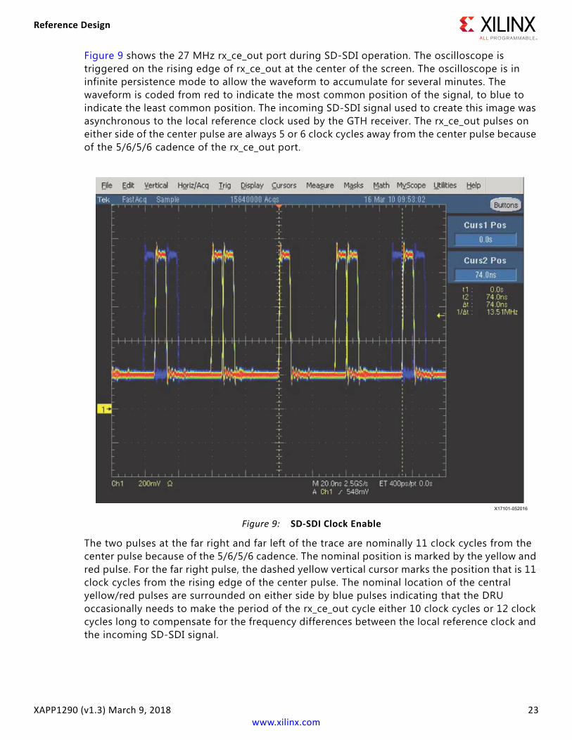
Figure 9 shows the 27 MHz rx_ce_out port during SD-SDI operation. The oscilloscope is triggered on the rising edge of rx_ce_out at the center of the screen. The oscilloscope is in infinite persistence mode to allow the waveform to accumulate for several minutes. The waveform is coded from red to indicate the most common position of the signal, to blue to indicate the least common position. The incoming SD-SDI signal used to create this image was asynchronous to the local reference clock used by the GTH receiver. The rx_ce_out pulses on either side of the center pulse are always 5 or 6 clock cycles away from the center pulse because of the 5/6/5/6 cadence of the rx_ce_out port.
The two pulses at the far right and far left of the trace are nominally 11 clock cycles from the center pulse because of the 5/6/5/6 cadence. The nominal position is marked by the yellow and red pulse. For the far right pulse, the dashed yellow vertical cursor marks the position that is 11 clock cycles from the rising edge of the center pulse. The nominal location of the central yellow/red pulses are surrounded on either side by blue pulses indicating that the DRU occasionally needs to make the period of the rx_ce_out cycle either 10 clock cycles or 12 clock cycles long to compensate for the frequency differences between the local reference clock and the incoming SD-SDI signal.
X-Ref Target - Figure 9
Figure 9: SD-SDI Clock Enable
Reference Design
XAPP1290 (v1.3) March 9, 2018 24www.xilinx.com
The SD-SDI DRU is supplied with the example SDI design as the encrypted, pre-generated file nidru_20_wrapper.vhd. The encryption used on the DRU is compatible with most synthesis and simulation software.
Transmitting SD-SDI
As with reception of SD-SDI, transmission of the slow 270 Mb/s SD-SDI bit rate is not directly supported by the GTH transmitter.To transmit the SD-SDI signal, the GTH TX is configured for a line rate of 2.97 Gb/s. The SDI core replicates each bit to be transmitted 11 times so that the data out of the SDI core and into the gth_txn_out port of the GTH Wizard IP contains 11 consecutive copies of each bit. The resulting signal output by the GTH transmitter is a valid 270 Mb/s SD-SDI signal.
Generating an SD-SDI Recovered Clock
In SD-SDI mode, the rxusrclk of the GTH receiver is not a recovered clock because the CDR unit is locked to the frequency of the reference clock, not to the SD-SDI bit stream. The only signal available that indicates the data rate of the incoming SD-SDI bit stream is the 27 MHz rx_ce_out output of the SDI wrapper.
For some video applications, particularly those that do not need to retransmit the recovered video over an SDI interface, the rx_ce_out port might be sufficient as a recovered clock. Typically, this signal is used as a clock enable to downstream modules that are clocked with the rxusrclk from the GTH RX. This is how the SDI data path in the SDI core works - using the rx_ce_out port as a clock enable.
If the received video data is to be retransmitted as an SD-SDI signal using a GTH transmitter, a low-jitter recovered clock is required. The recovered clock must have low-enough jitter that it can be used as a reference clock for the PLL generating the serial clock for the GTH transmitter. The frequency of the recovered clock must be 148.5 MHz so that the GTH transmitter can use 11X oversampling to transmit the 270 Mb/s SD-SDI data. This requires the use of an external low-bandwidth PLL. The bandwidth of the mixed-mode clock manager (MMCM) in a Kintex UltraScale FPGA is too high to adequately filter out the large amounts of low-frequency jitter present on the rx_ce_out port from the SDI receiver. The Texas Instruments LMH1983 and the Silicon Labs Si5328 can both perform this function. Both of these devices can take in the rx_ce_out port as a 27 MHz reference and multiply it up to 148.5 MHz while also filtering out the jitter. The resulting clock is suitable for use as a reference clock for the GTH transmitter. The pass-through demo included with the example SDI design uses an Si5328 to generate a 148.5 MHz reference clock for the GTH transmitter from the 27 MHz rx_ce_out port in this manner in SD-SDI mode. When retransmitting HD-SDI or 3G-SDI the Si5328 is reprogrammed to filter jitter from the rxusrclk output of the GTH receiver, doubling its frequency in the case of HD-SDI, producing a low-jitter 148.5 MHz reference clock for the GTH transmitter.
Another option is to use an external genlock PLL and lock it to the video sync signals from the recovered video. The output of the genlock PLL will be an SD-SDI recovered clock.
Sometimes a recovered clock is required to drive external video application-specific standard product (ASSP) devices. In SD-SDI mode, such a clock will probably need a frequency of 27 MHz and have lower jitter than is present on the rx_ce_out port, but doesn't require very low jitter as is the case when producing a GTH TX reference clock. The techniques mentioned previously can
Reference Design
XAPP1290 (v1.3) March 9, 2018 25www.xilinx.com
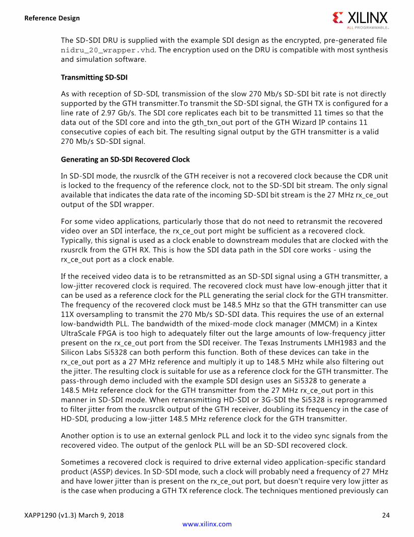
be used, but it may be preferable to generate such a recovered clock entirely in the FPGA without requiring external components. Unfortunately, the jitter on the rx_ce_out port is too high to allow it to be used directly as a reference clock input to a Kintex UltraScale FPGA MMCM. However, there is a way to generate a recovered SD-SDI clock using a spare GTH TX as shown in Figure 10.
The control module's recclk_txdata port can be connected to the gtwiz_userdata_tx_in port of a spare GTH TX of GTH Wizard IP. The GTH TX must use the same reference clock as the GTH RX that is receiving the SDI input signal. The rxusrclk can be routed to gtrefclk0_in of the GT Wizard IP and the txpllclksel_in must be set to use CPLL. The GTH TX must be configured for a line rate of 2.97 Gb/s with no encoding and with a 20-bit gtwiz_userdata_tx_in port.
When configured in this manner, the serial output of the GTH TX will be a 270 MHz clock that is frequency locked to the incoming SD-SDI signal, providing a true recovered clock for SD-SDI. The GTH TX serial output pins can be connected to a global or regional clock LVDS input of the Kintex UltraScale FPGA, with appropriate care to properly terminate the CML outputs and translate them to LVDS. Then the 270 MHz clock can be used in whatever manner is required in the FPGA. For example, it can be divided by 10 to get a 27 MHz recovered clock to drive internal or external video data paths. The signal has low enough jitter that it can be used as a reference clock to an MMCM.
X-Ref Target - Figure 10
Figure 10: Using a GTH TX to Generate an SD-SDI Recovered Clock
Reference Design
XAPP1290 (v1.3) March 9, 2018 26www.xilinx.com
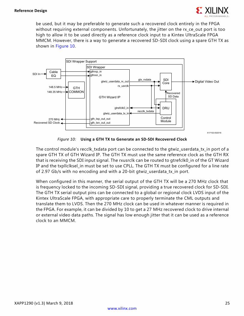
The recclk_txdata port of the DRU is not wired from the SDI control module to an output port of the SDI wrapper. However, if an application needs to use this feature, the SDI wrapper can be edited to add this output port. Figure 11 shows the use of a GTH transmitter to generate a SD-SDI recovered clock.
The GTH TX that is used to generate the recovered SD-SDI clock does not have to be configured for SDI. It only needs to be configured to always run a line rate of 2.97 Gb/s with no encoding. The data supplied to the gtwiz_userdata_tx_in port of the GTH Wizard IP from the recclk_txdata port of the control module creates a 270 MHz clock on the GTH TX serial output pins. The edges of the generated clock vary by plus or minus one bit time of the 2.97 Gb/s line rate to modify the frequency of the output signal so as to exactly match the bit rate of input SD-SDI signal. Thus, the cycle-to-cycle jitter on the 270 MHz clock generated by the GTH TX will be ±337 ps plus whatever jitter is inherent in the GTH TX output signal (1 bit time at 2.97 Gb/s is 337 ps). This can be seen in Figure 11. The top trace is the 270 MHz clock generated by the GTH TX. The scope was triggered on the rising edge of the recovered clock at the center of the screen. Looking at the rising edges of the cycles on either side of the trigger point, it is easy to see the ±337 ps cycle-to-cycle jitter because these rising edges each have three discrete rising points. The bottom trace in Figure 11 is the SD-SDI that is being retransmitted by another GTH TX.
X-Ref Target - Figure 11
Figure 11: Recovered SD-SDI Clock from GTH Transceiver
Reference Design
XAPP1290 (v1.3) March 9, 2018 27www.xilinx.com
Automatic RX SDI Mode Detection
The SDI core can automatically determine the SDI mode (SD, HD, or 3G-SDI) of the SDI signal coming into the GTH RX. When it is not locked to the current SDI input signal, the SDI core sequences the GTH RX through the three different SDI modes until it detects recognizably good SDI data on the rxdata output port of the GTH. At that point, the SDI core indicates that the GTH CDR is locked to the SDI signal by asserting its rx_mode_locked_out port. It also indicates which SDI mode the RX is locked to on its sdi_mode_out port.
It is important to understand that the rx_mode_locked signal is an indication of whether or not the SDI core thinks that the GTH RX is locked to the SDI signal, and nothing more. It is really just an indication of whether the SDI core's mode search state machine is still searching for the correct SDI mode or not. Because of this, rx_mode_locked should not be considered as an absolute indicator as to the locked status of the SDI RX.
When the GTH RX is not locked to the input SDI signal and the SDI core is actively controlling GTH RX in an effort to determine the correct SDI mode, the rx_mode_locked signal may briefly become asserted. This will happen if the incoming data randomly appears to be a valid SAV sequence. If an SAV sequence is detected, the SDI core will assert rx_mode_locked and pause the mode search expecting more good data to be received. If, however, good data is not received within a specific timeout period, the rx_mode_locked signal will be negated and the SDI mode search will resume.
The SDI mode search algorithm only attempts to lock to SDI modes that are enabled by the rx_mode_en_in port of the SDI wrapper. This 3-bit port has unary bits that enable HD-SDI (bit 0), SD-SDI (bit 1), 3G-SDI (bit 2).
The rx_mode_en_in port can be changed dynamically. However, if the SDI RX is already locked to a mode that becomes disabled by dynamically clearing its bit on the rx_mode_en_in port, this will not automatically kick the SDI RX out of that mode. The SDI RX will remain locked in the SDI mode until the input SDI signal changes or the SDI RX is reset, forcing the SDI mode search algorithm to try and identify the SDI mode using the new settings of the rx_mode_en_in port.
The automatic SDI mode search algorithm of the SDI core can be disabled. The mode search algorithm will only be enabled when the rx_mode_detect_en_in port is logic High. If this port is logic Low, then the SDI RX must be told what SDI mode to operate in through the rx_forced_mode_in port. When rx_mode_detect_en_in is logic Low and the SDI mode search algorithm is disabled, the SDI RX will be in the mode specified by the rx_forced_mode_in port and the rx_mode_locked output will always be logic High. Thus, rx_mode_locked cannot be used as a locked indicator or a data valid indicator in this mode. When the mode search algorithm is disabled, dynamic changes on rx_forced_mode_in will cause the SDI control logic to dynamically change the settings of the GTH RX as necessary for the new SDI mode.
RX Bit Rate Detection
The SDI core can automatically determine the SDI mode (SD-SDI, HD-SDI or 3G-SDI) of the SDI signal received by the GTH RX. When it is not locked to the current SDI input signal, the SDI core sequences the GTH RX through the three different SDI modes until it detects recognizably good SDI data on the gtwiz_userdata_rx_out output port of the GTH Wizard IP. At that point, the SDI
Reference Design
XAPP1290 (v1.3) March 9, 2018 28www.xilinx.com
core indicates that it is locked to the SDI signal by asserting its rx_mode_locked output. It also indicates which SDI mode the RX is locked to on its rx_mode output port.
When the SDI core is in HD-SDI or 3G-SDI, it has no way of determining if the bit rate of the input SDI signal is bitrate/1 or bitrate/1.001 (e.g for 3G-SDI; 2.97 Gb/s or 2.97/1.001 Gb/s). However, the control module supplied with the example SDI design contains a bit rate detector that can distinguish between 1.485 Gb/s and 1.485/1.001 Gb/s and between 2.97 Gb/s and 2.97/1.001 Gb/s. The SDI wrapper output port rx_m_out is logic Low when the input SDI signal bit rate is bitrate/1 and rx_m_out is logic High when the input SDI signal bit rate is bitrate/1.001.
For the bit rate detection feature to work, the SDI wrapper must be supplied with a fixed-frequency clock on its rx_fxdclk_in input port. The frequency of this clock should be at least 10 MHz. If the frequency is over 150 MHz, it might be difficult to meet timing in the bit rate detection logic. The SDI wrapper parameter FXDCLK_FREQ must be used to specify the frequency of the clock connected to the rx_fxdclk_in port. The value of FXDCLK_FREQ must be set equal to the frequency of the fixed frequency clock in Hz.
Example SDI Demonstrations
This section provides an overview of the example SDI design. The procedures for running the reference design from setup to results are located under Reference Design Steps.
Figure 12 shows the block diagram of the example SDI design, SDI channel 0, which is connected to the first GTH transceiver in the Quad.
X-Ref Target - Figure 12
Figure 12: SDI Example Design Block Diagram
Reference Design
XAPP1290 (v1.3) March 9, 2018 29www.xilinx.com
The example SDI design implements a pair of SDI RX and SDI TX interfaces on the KCU105 board. It uses the Fidus inrevium 6G/12G SDI FPGA Mezzanine Card connected to the HPC FMC connector of the KCU105 board to implement the complete interface. The example SDI design has a single SDI transmitter driven by a video generator. It supports operation at SD-SDI, HD-SDI and 3G-SDI (levels A and B). The SDI transmitter is controlled by the LogiCORE IP Virtual Input/Output core (VIO). The example SDI design also has a single SDI receiver which can operate in the same modes as the transmitter. The status of the SDI receiver is monitored by a Vivado analyzer VIO module. The data streams, line numbers, and video timing signals output by the SDI receiver are captured by the Integrated Logic Analyzer (ILA) IP core and can be inspected in the Vivado logic analyzer tool.
The SDI TX is driven by a video pattern generator. The SDI mode, video format, and video pattern of SDI transmitter can be selected using a Vivado VIO window in the Vivado Hardware Manager. The status of the SDI RX can be monitored using a different Vivado VIO window. And the video data received by the SDI RX can be captured and viewed using a Vivado ILA window.
The Fidus inrevium 6G/12G SDI FPGA Mezzanine Card has 5 connectors for the SDI interfaces. See Figure 13. The two rightmost connectors are the only uni-directional SDI interfaces. The rightmost being the CH0 TX and the other CH0 RX. These connectors are the only ones which are used in this demonstration. The second, third and fourth SDI interfaces have only a single connector each, CH1, CH2 and CH3.These are bidirectional interfaces and can be controlled by F_CHn_DIR pins of the FMC card.
The inrevium SDI FMC board has 148.5 MHz and 148.5/1.001 MHz oscillators which this demo uses to supply reference clocks to the QPLL0 and the QPLL1 that goes to each transceiver. The 148.5 MHz reference clock is used by the QPLL0 and the 148.5/1.001 MHz reference clock is used by the QPLL1. The GTH transmitters are dynamically switched between the serial clock from the QPLL0 and the QPLL1 in order to support all SDI bit rates.
The LMH1983 device on the inrevium board supplies a 27 MHz clock to the FPGA that is used for the DRP clock and fixed frequency clock required by the control module.
To make it easier to increase the SDI interface up to four in this demo, a four SDI channel wrapper (kugth_3gsdi_4ch_wrapper.v) was created which instantiates one SDI wrapper support and three SDI wrapper. The video generator, main and RX Vivado VIOs where all placed inside a Verilog Generate statement to easily increase the number of channels.
Software Application
Fidus inrevium 6G/12G SDI FPGA Mezzanine Card Controller Software
The example SDI design includes IP-integrator based 6G/12G SDI FMC controller software to provide access and control to the I2C and SPI devices on the FMC card. The controller is instantiated in the project hierarchy as system_basic, and is composed of SPI, IIC, and GPIO IP cores and basic IP components in order to run a MicroBlaze™ application. The GPIO allows FMC channel selection during configuration and to gives access to the initialization done state.
To initialize the FPGA on the KCU105 board, The 6G/12G SDI FMC controller software performs three tasks:
Reference Design
XAPP1290 (v1.3) March 9, 2018 30www.xilinx.com
1. Configure and select the GTH transceiver 148.35 MHz and 148.5 MHz reference clocks.
2. Initialize the generic SPI bus devices (cable driver, equalizer and reclocker) which includes setting the output voltage swing, input equalization factor, and muting one of two SDI cable driver outputs.
3. Initialize the Macom cable equalizer and reclocker located on the Fidus inrevium 6G/12G SDI FPGA Mezzanine Card based on the die ID number for these devices. Special SPI register initialization is needed for different die ID numbers to ensure error-free SDI reception.
Note: Errata 235x4-ERR-001-A, 23145-ERR-001-A, 23145-ERR-001-C, 23145-ERR-001-D and M235x4-ERR-001-C were considered when the 6G/12G SDI FMC controller software was written.
The controller software Main Menu allows options to select and modify devices. The controller software interface is shown here:
------------------------- FIDUS Main Menu -------------------------
Select option 1 = Re-Init 2 = IIC Dev Select 3 = SPI CH0 Select 4 = SPI CH1 Select 5 = SPI CH2 Select 6 = SPI CH3 Select ? = help------------------>
Tool Flow and Verification
Table 2 indicates the tool flow and verification procedures used for the provided reference design.
Table 2: Reference Design Matrix
Parameter Description
General
Target deviceKintex UltraScale Devices. The example SDI design targets the KCU105 evaluation board containing the Kintex UltraScale XCKU040-2FFVA1156C FPGA.
Source code provided Yes
Source code format Verilog
Design uses code and IP cores from existing Xilinx application notes and reference designs or third party
Yes, IP cores from the Vivado IP Catalog.
Simulation
Functional simulation performed No
Timing simulation performed No
Test bench used for functional and timing simulations No
Requirements
XAPP1290 (v1.3) March 9, 2018 31www.xilinx.com
RequirementsThis section lists the requirements for running the example SDI design.
Hardware
• KCU105 Evaluation Kit [Ref 8] which includes:
° KCU105 evaluation board, revision 1.0 or later [Ref 9]
° Two USB cables, standard-A plug to micro-B plug
° Power Supply: 100 VAC–240 VAC input, 12 VDC 5.0A output
• Fidus inrevium 6G/12G SDI FPGA Mezzanine Card (6G/12G SDI FMC), part number TB-FMCH-12GSDI, Fidus Systems Inc. [Ref 10]
• Two HD-BNC plug to BNC plug cables
• SDI Source and Sink such as the PHABRIX SxE Eye and Jitter video test generator monitor and analyzer [Ref 14]
Computer
One computer is required for running Vivado Design Suite, configuring the FPGA, and running the GUI interface to control and monitor the example SDI design. It can be a laptop or desktop computer with Microsoft Windows 7 operating system.
Test bench format N/A
Simulator software/version used N/A
SPICE/IBIS simulations N/A
Implementation
Synthesis software tools/versions used Vivado Design Suite 2018.1
Implementation software tools/versions used Vivado Design Suite 2018.1
Static timing analysis performed Yes
Hardware Verification
Hardware verified Yes
Hardware platform used for verification KCU105 evaluation board and TB-FMCH-12GSDI board
Table 2: Reference Design Matrix
Parameter Description
Reference Design Steps
XAPP1290 (v1.3) March 9, 2018 32www.xilinx.com
Software
• Vivado® Design Suite 2018.1
• USB UART drivers (CP210x VCP drivers)
• Tera Term terminal emulator
• 6G/12G SDI FMC software controller (included with the example SDI design) for controlling the 6G/12G SDI FMC
Reference Design Files
Download the reference design files.
Licensing
Ensure that the licenses used by the IP cores used by the example SDI design are installed.
Reference Design Steps
Setup
Set Up Host Computer
If not already installed:
1. Install Vivado Design Suite version 2018.1 or later.
2. Download and install Tera Term. Follow the procedure in Tera Term Terminal Emulator Installation Guide (UG1036) [Ref 11].
3. Download and install the UART drivers. Follow the instructions in Silicon Labs CP210x USB-to-UART Installation Guide (UG1033) [Ref 12]
TIP: The UART communication settings are set up later in this procedure.
Set Up KCU105 Board
Follow these steps to configure the FPGA with a pre-compiled BIT file.
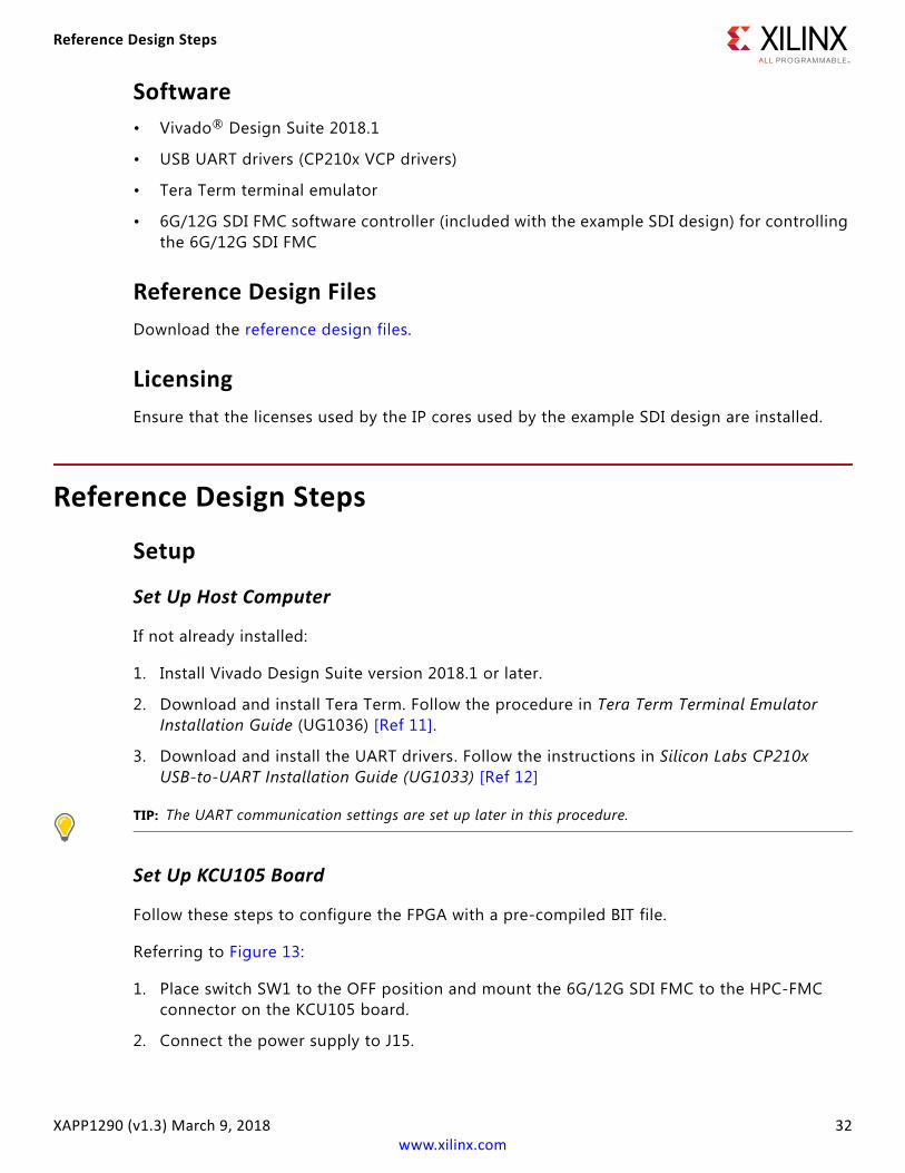
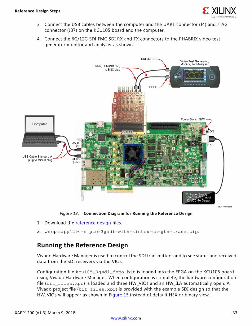
Referring to Figure 13:
1. Place switch SW1 to the OFF position and mount the 6G/12G SDI FMC to the HPC-FMC connector on the KCU105 board.
2. Connect the power supply to J15.
Reference Design Steps
XAPP1290 (v1.3) March 9, 2018 33www.xilinx.com
3. Connect the USB cables between the computer and the UART connector (J4) and JTAG connector (J87) on the KCU105 board and the computer.
4. Connect the 6G/12G SDI FMC SDI RX and TX connectors to the PHABRIX video test generator monitor and analyzer as shown.
1. Download the reference design files.
2. Unzip xapp1290-smpte-3gsdi-with-kintex-us-gth-trans.zip.
Running the Reference Design
Vivado Hardware Manager is used to control the SDI transmitters and to see status and received data from the SDI receivers via the VIOs.
Configuration file kcu105_3gsdi_demo.bit is loaded into the FPGA on the KCU105 board using Vivado Hardware Manager. When configuration is complete, the hardware configuration file (bit_files.xpr) is loaded and three HW_VIOs and an HW_ILA automatically open. A Vivado project file (bit_files.xpr) is provided with the example SDI design so that the HW_VIOs will appear as shown in Figure 15 instead of default HEX or binary view.
X-Ref Target - Figure 13
Figure 13: Connection Diagram for Running the Reference Design
Wally
Reference Design Steps
XAPP1290 (v1.3) March 9, 2018 34www.xilinx.com
To run the reference design:
1. Power on the KCU105 board.
2. Connect to the KCU105 board system controller software and set VADJ to 1.8V:
a. On the computer, run Tera Term. (115200, 8, N, 1) and set the COM port to the one communicating with the KCU105 board system controller.
Note: Connector J4 (UART) provides access to the Zynq®-7000 All Programmable SoC system controller UART and to the FPGA UART. In the Windows Device Manager, the Enhanced COM port associated with the CP210x, is the one connected to the System Controller.
3. After Tera Term is connected to the enhanced COM port, power cycle the KCU105 board to refresh the system controller menu in the UART terminal.
4. Select this option in the system controller menu.
4. Adjust FPGA Mezzanine Card (FMC) Settings
5. In the next menu, select:
4. Set FMC VADJ to 1.8V
6. Look for the VADJ power good on DS19 LED located near the power switch on the KCU105 board (Figure 14).
7. In the Vivado Tcl Console, Enter:
cd <unzip_dir>\ready_for_downloadsource bit_files.tcl
8. Wait for the project to load and the FPGA to program.
Note: If the SDI RX is not locking, verify the VADJ power to FMCH port is at 1.8V VADJ. Power good is indicated by DS19 LED on the KCU105 board. If the LED is off, the VADJ power can be set through the system controller menu.
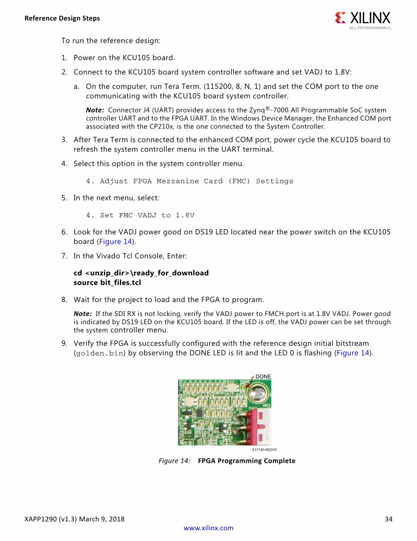
9. Verify the FPGA is successfully configured with the reference design initial bitstream (golden.bin) by observing the DONE LED is lit and the LED 0 is flashing (Figure 14).
X-Ref Target - Figure 14
Figure 14: FPGA Programming Complete
Reference Design Steps
XAPP1290 (v1.3) March 9, 2018 35www.xilinx.com
The example SDI design uses the GPIO LEDs shown in Figure 14 to indicate status. Table 3 shows the status type assigned to each LED.
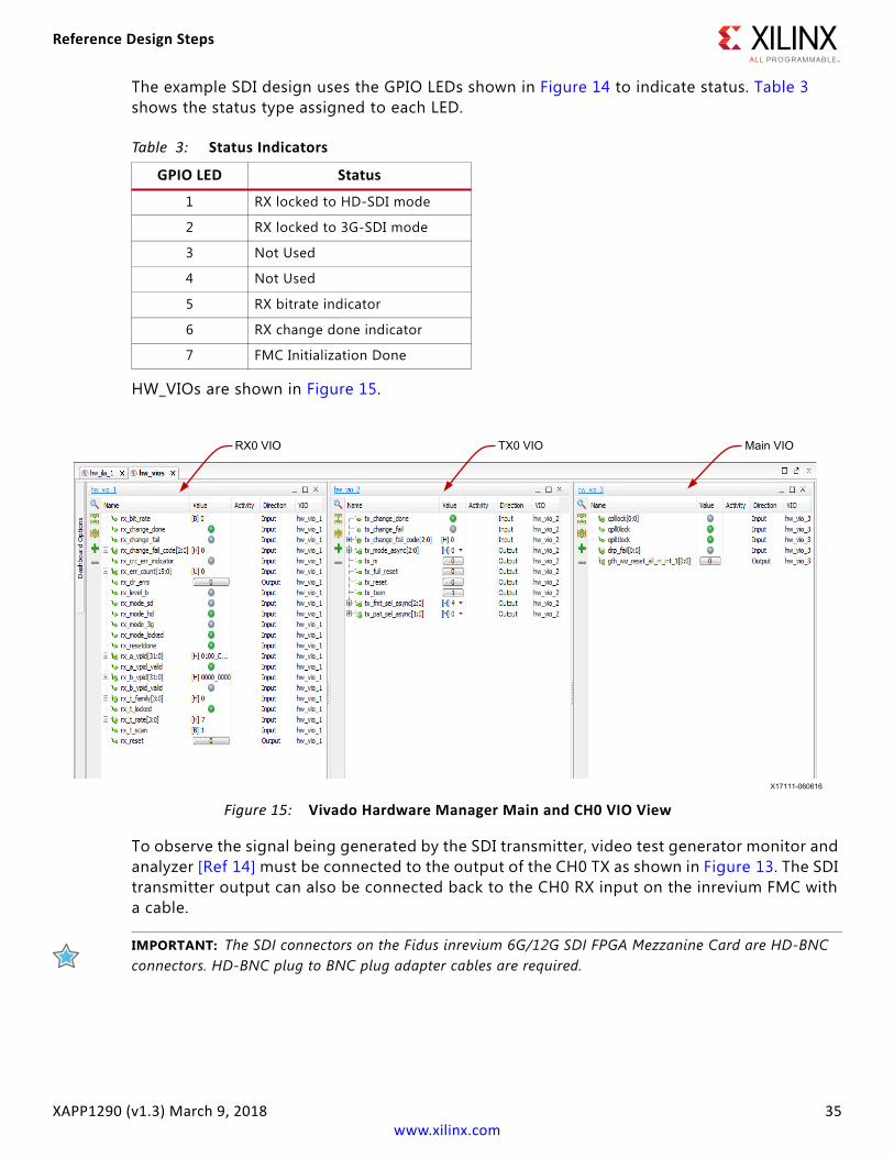
HW_VIOs are shown in Figure 15.
To observe the signal being generated by the SDI transmitter, video test generator monitor and analyzer [Ref 14] must be connected to the output of the CH0 TX as shown in Figure 13. The SDI transmitter output can also be connected back to the CH0 RX input on the inrevium FMC with a cable.
IMPORTANT: The SDI connectors on the Fidus inrevium 6G/12G SDI FPGA Mezzanine Card are HD-BNC connectors. HD-BNC plug to BNC plug adapter cables are required.
Table 3: Status Indicators
GPIO LED Status
1 RX locked to HD-SDI mode
2 RX locked to 3G-SDI mode
3 Not Used
4 Not Used
5 RX bitrate indicator
6 RX change done indicator
7 FMC Initialization Done
X-Ref Target - Figure 15
Figure 15: Vivado Hardware Manager Main and CH0 VIO View
Reference Design Steps
XAPP1290 (v1.3) March 9, 2018 36www.xilinx.com
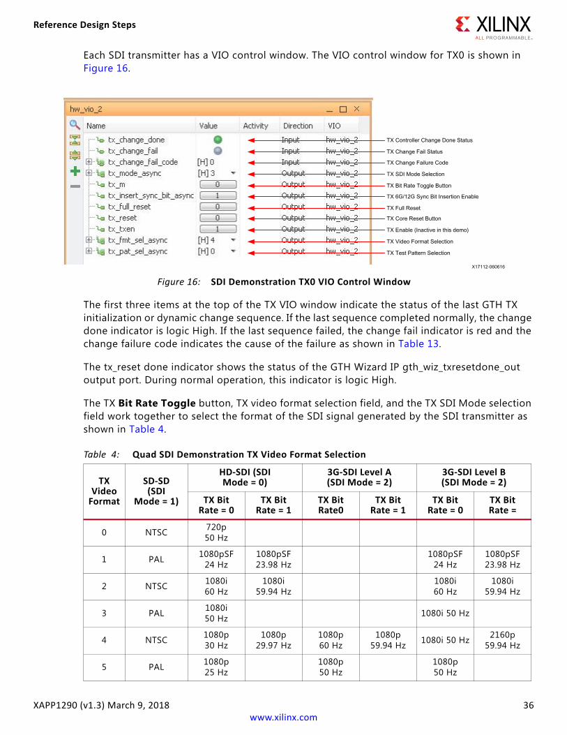
Each SDI transmitter has a VIO control window. The VIO control window for TX0 is shown in Figure 16.
The first three items at the top of the TX VIO window indicate the status of the last GTH TX initialization or dynamic change sequence. If the last sequence completed normally, the change done indicator is logic High. If the last sequence failed, the change fail indicator is red and the change failure code indicates the cause of the failure as shown in Table 13.
The tx_reset done indicator shows the status of the GTH Wizard IP gth_wiz_txresetdone_out output port. During normal operation, this indicator is logic High.
The TX Bit Rate Toggle button, TX video format selection field, and the TX SDI Mode selection field work together to select the format of the SDI signal generated by the SDI transmitter as shown in Table 4.
X-Ref Target - Figure 16
Figure 16: SDI Demonstration TX0 VIO Control Window
Table 4: Quad SDI Demonstration TX Video Format Selection
TX Video
Format
SD-SD(SDI
Mode = 1)
HD-SDI (SDIMode = 0)
3G-SDI Level A(SDI Mode = 2)
3G-SDI Level B(SDI Mode = 2)
TX BitRate = 0
TX BitRate = 1
TX BitRate0
TX BitRate = 1
TX BitRate = 0
TX BitRate =
0 NTSC 720p50 Hz
1 PAL 1080pSF24 Hz
1080pSF23.98 Hz
1080pSF24 Hz
1080pSF23.98 Hz
2 NTSC 1080i60 Hz
1080i59.94 Hz
1080i60 Hz
1080i59.94 Hz
3 PAL 1080i50 Hz 1080i 50 Hz
4 NTSC 1080p30 Hz
1080p29.97 Hz
1080p60 Hz
1080p59.94 Hz 1080i 50 Hz 2160p
59.94 Hz
5 PAL 1080p25 Hz
1080p50 Hz
1080p50 Hz
Reference Design Steps
XAPP1290 (v1.3) March 9, 2018 37www.xilinx.com
The TX video pattern value selects the video test pattern generated by the video pattern generator driving the SDI TX. In HD-SDI and 3G-SDI mode, three test patterns are available:
• 0 = SMPTE RP 219 color bars
• 1 and 3 = SDI pathological checkfield
• 2 = 75% color bars
In SD-SDI mode, two test patterns are available:
• 0 and 2 = SMPTE EG 1 color bars
• 1 and 3 = SDI pathological checkfield
In addition to the tx_mode_in values specified in Table 4, TX_MODE can also be set to 3'b011 to stream 3G-SDI Level B patterns.
6 NTSC 1080p24 Hz
1080p23.98 Hz
7 PAL 720p60 Hz
720p59.94 Hz
Table 4: Quad SDI Demonstration TX Video Format Selection (Cont’d)
TX Video
Format
SD-SD(SDI
Mode = 1)
HD-SDI (SDIMode = 0)
3G-SDI Level A(SDI Mode = 2)
3G-SDI Level B(SDI Mode = 2)
TX BitRate = 0
TX BitRate = 1
TX BitRate0
TX BitRate = 1
TX BitRate = 0
TX BitRate =
Reference Design Steps
XAPP1290 (v1.3) March 9, 2018 38www.xilinx.com
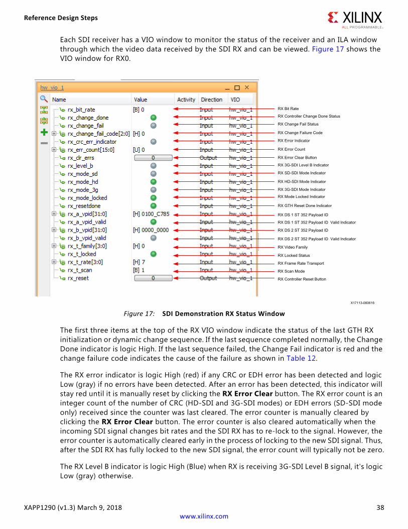
Each SDI receiver has a VIO window to monitor the status of the receiver and an ILA window through which the video data received by the SDI RX and can be viewed. Figure 17 shows the VIO window for RX0.
The first three items at the top of the RX VIO window indicate the status of the last GTH RX initialization or dynamic change sequence. If the last sequence completed normally, the Change Done indicator is logic High. If the last sequence failed, the Change Fail indicator is red and the change failure code indicates the cause of the failure as shown in Table 12.
The RX error indicator is logic High (red) if any CRC or EDH error has been detected and logic Low (gray) if no errors have been detected. After an error has been detected, this indicator will stay red until it is manually reset by clicking the RX Error Clear button. The RX error count is an integer count of the number of CRC (HD-SDI and 3G-SDI modes) or EDH errors (SD-SDI mode only) received since the counter was last cleared. The error counter is manually cleared by clicking the RX Error Clear button. The error counter is also cleared automatically when the incoming SDI signal changes bit rates and the SDI RX has to re-lock to the signal. However, the error counter is automatically cleared early in the process of locking to the new SDI signal. Thus, after the SDI RX has fully locked to the new SDI signal, the error count will typically not be zero.
The RX Level B indicator is logic High (Blue) when RX is receiving 3G-SDI Level B signal, it's logic Low (gray) otherwise.
X-Ref Target - Figure 17
Figure 17: SDI Demonstration RX Status Window
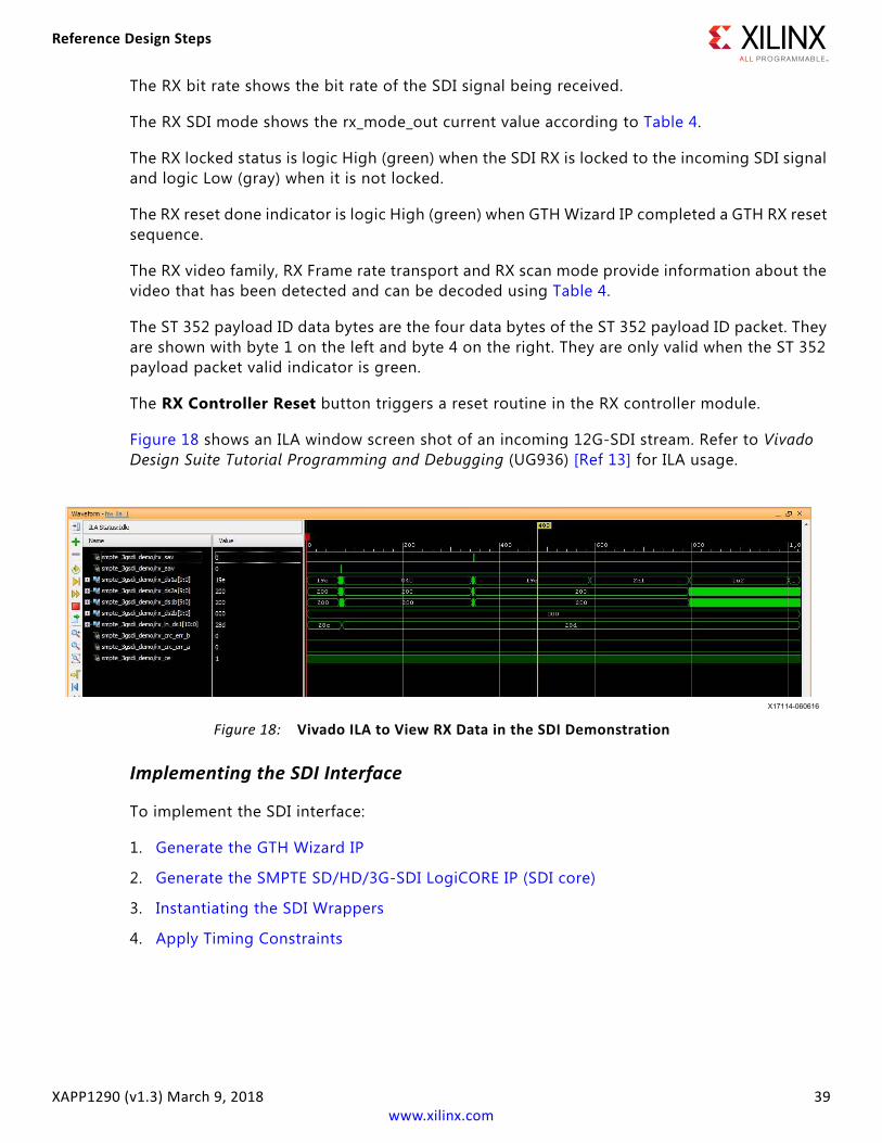
Reference Design Steps
XAPP1290 (v1.3) March 9, 2018 39www.xilinx.com
The RX bit rate shows the bit rate of the SDI signal being received.
The RX SDI mode shows the rx_mode_out current value according to Table 4.
The RX locked status is logic High (green) when the SDI RX is locked to the incoming SDI signal and logic Low (gray) when it is not locked.
The RX reset done indicator is logic High (green) when GTH Wizard IP completed a GTH RX reset sequence.
The RX video family, RX Frame rate transport and RX scan mode provide information about the video that has been detected and can be decoded using Table 4.
The ST 352 payload ID data bytes are the four data bytes of the ST 352 payload ID packet. They are shown with byte 1 on the left and byte 4 on the right. They are only valid when the ST 352 payload packet valid indicator is green.
The RX Controller Reset button triggers a reset routine in the RX controller module.
Figure 18 shows an ILA window screen shot of an incoming 12G-SDI stream. Refer to Vivado Design Suite Tutorial Programming and Debugging (UG936) [Ref 13] for ILA usage.
Implementing the SDI Interface
To implement the SDI interface:
1. Generate the GTH Wizard IP
2. Generate the SMPTE SD/HD/3G-SDI LogiCORE IP (SDI core)
3. Instantiating the SDI Wrappers
4. Apply Timing Constraints
X-Ref Target - Figure 18
Figure 18: Vivado ILA to View RX Data in the SDI Demonstration
Reference Design Steps
XAPP1290 (v1.3) March 9, 2018 40www.xilinx.com
Generate the GTH Wizard IP
The UltraScale FPGAs Transceivers Wizard is used to generate the GTH Wizard IP. The GTH Wizard IP is a hierarchy of wrappers that optionally include the GTH COMMON primitive and helper logic for GTH TX and RX clocking, GTH transceiver reset, and data width sizing. For SDI applications, all helper logic should be included with the GTH Wizard IP. Exclude the GTH COMMON primitive from the GTH Wizard IP because it is instantiated in the SDI wrapper support module. Each instance of GTH Wizard IP is located using a set_property LOC command to a specific GTHE3_CHANNEL location. For this reason, multiple GTH Wizard IP must be generated for each SDI channel in the design. Also, the SDI wrapper support module must be instantiated once for each GTH Quad containing transceivers implementing SDI interfaces. If only the CPLL is used to clock the GTH transceivers, an instance of the SDI wrapper support module is not required. An instance of the IBUFDS_GTE3 primitive must be instantiated to bring the differential reference clock to the CPLL.
TIP: The SDI demonstration applications supplied with the example SDI design provide examples of how to instantiate multiple GTH Wizard IP cores in the SDI wrapper module.
Note: Version 1.7 of the UltraScale FPGAs Transceivers Wizard comes with HD-SDI and 3G-SDI presets, the 3G-SDI presets will be used as baseline moving forward.
To generate the GTH wrapper:
1. In Vivado Design Suite, open the project.
2. Open the IP Catalog and select the IP at FPGA Features and Design > I/O Interfaces > UltraScale FPGAs Transceivers Wizard.
3. Double-click the IP to launch the UltraScale FPGAs Transceivers Wizard. The Wizard launches with the Basic tab open as shown in Figure 19.
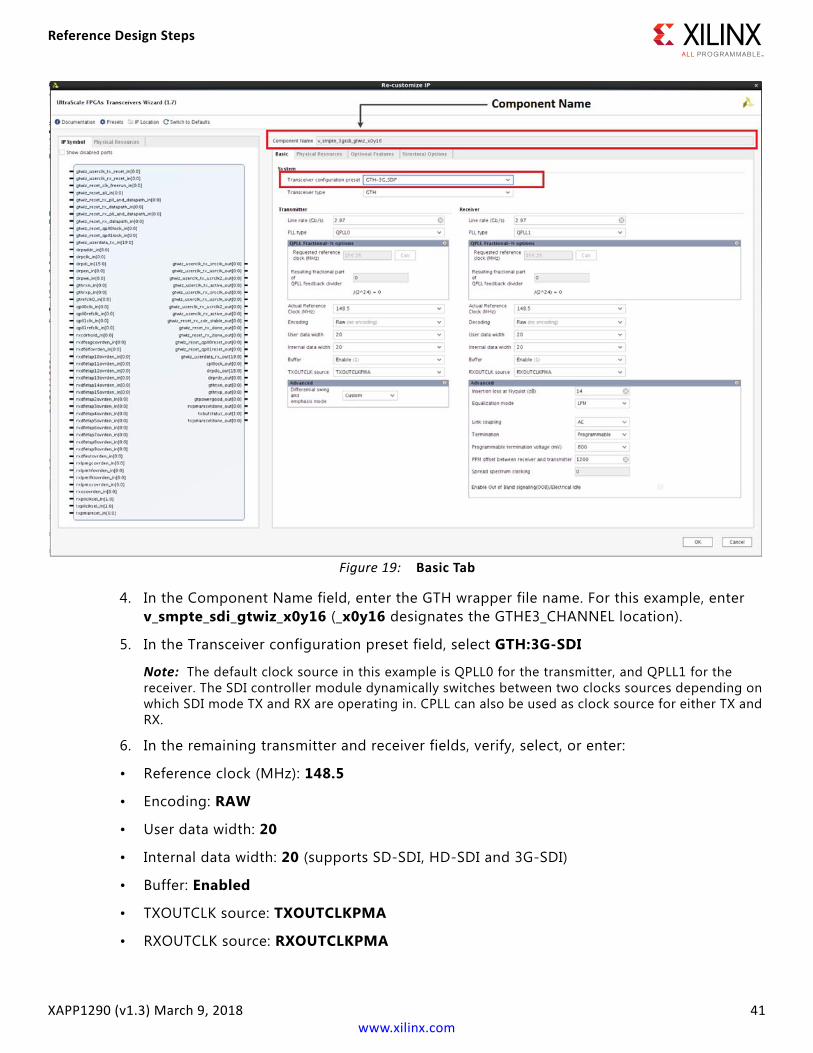
Reference Design Steps
XAPP1290 (v1.3) March 9, 2018 41www.xilinx.com
4. In the Component Name field, enter the GTH wrapper file name. For this example, enter v_smpte_sdi_gtwiz_x0y16 (_x0y16 designates the GTHE3_CHANNEL location).
5. In the Transceiver configuration preset field, select GTH:3G-SDI
Note: The default clock source in this example is QPLL0 for the transmitter, and QPLL1 for the receiver. The SDI controller module dynamically switches between two clocks sources depending on which SDI mode TX and RX are operating in. CPLL can also be used as clock source for either TX and RX.
6. In the remaining transmitter and receiver fields, verify, select, or enter:
• Reference clock (MHz): 148.5
• Encoding: RAW
• User data width: 20
• Internal data width: 20 (supports SD-SDI, HD-SDI and 3G-SDI)
• Buffer: Enabled
• TXOUTCLK source: TXOUTCLKPMA
• RXOUTCLK source: RXOUTCLKPMA
X-Ref Target - Figure 19
Figure 19: Basic Tab
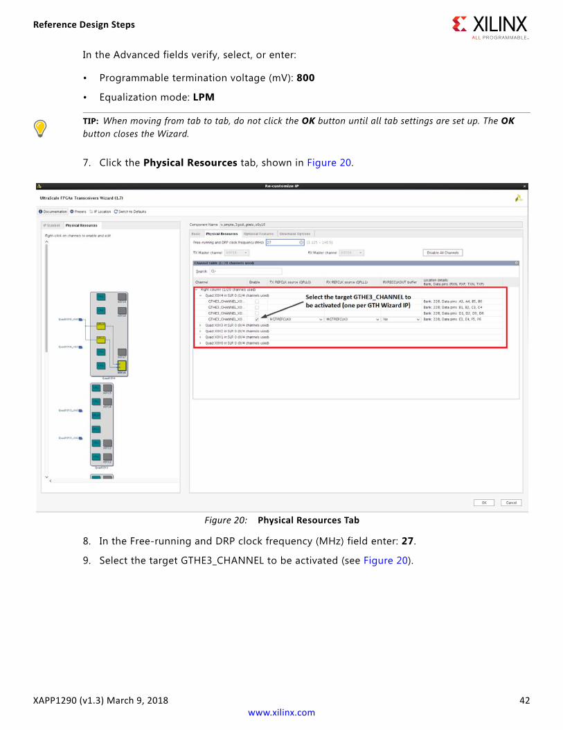
Reference Design Steps
XAPP1290 (v1.3) March 9, 2018 42www.xilinx.com
In the Advanced fields verify, select, or enter:
• Programmable termination voltage (mV): 800
• Equalization mode: LPM
TIP: When moving from tab to tab, do not click the OK button until all tab settings are set up. The OK button closes the Wizard.
7. Click the Physical Resources tab, shown in Figure 20.
8. In the Free-running and DRP clock frequency (MHz) field enter: 27.
9. Select the target GTHE3_CHANNEL to be activated (see Figure 20).
X-Ref Target - Figure 20
Figure 20: Physical Resources Tab
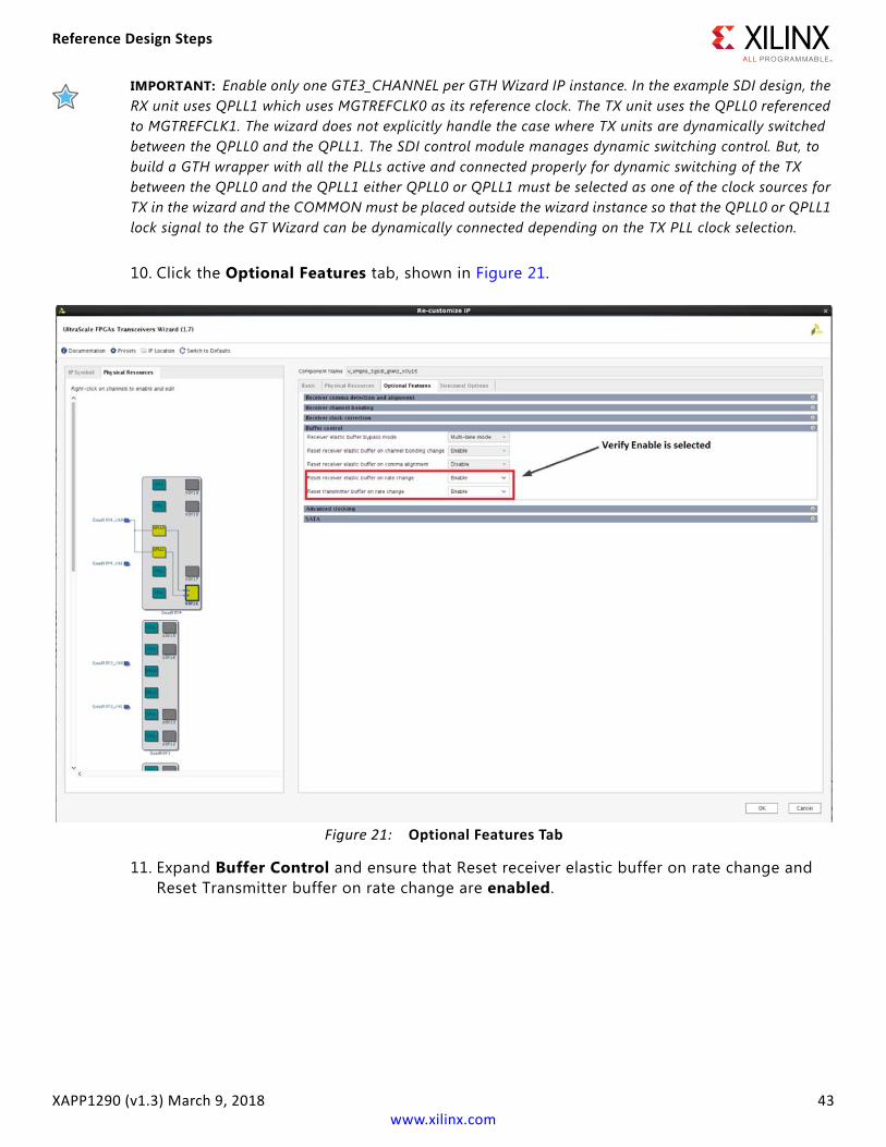
Reference Design Steps
XAPP1290 (v1.3) March 9, 2018 43www.xilinx.com
IMPORTANT: Enable only one GTE3_CHANNEL per GTH Wizard IP instance. In the example SDI design, the RX unit uses QPLL1 which uses MGTREFCLK0 as its reference clock. The TX unit uses the QPLL0 referenced to MGTREFCLK1. The wizard does not explicitly handle the case where TX units are dynamically switched between the QPLL0 and the QPLL1. The SDI control module manages dynamic switching control. But, to build a GTH wrapper with all the PLLs active and connected properly for dynamic switching of the TX between the QPLL0 and the QPLL1 either QPLL0 or QPLL1 must be selected as one of the clock sources for TX in the wizard and the COMMON must be placed outside the wizard instance so that the QPLL0 or QPLL1 lock signal to the GT Wizard can be dynamically connected depending on the TX PLL clock selection.
10. Click the Optional Features tab, shown in Figure 21.
11. Expand Buffer Control and ensure that Reset receiver elastic buffer on rate change and Reset Transmitter buffer on rate change are enabled.
X-Ref Target - Figure 21
Figure 21: Optional Features Tab
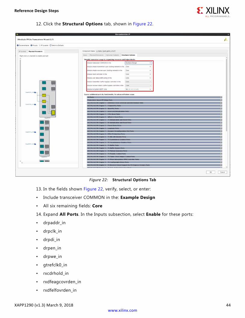
Reference Design Steps
XAPP1290 (v1.3) March 9, 2018 44www.xilinx.com
12. Click the Structural Options tab, shown in Figure 22.
13. In the fields shown Figure 22, verify, select, or enter:
• Include transceiver COMMON in the: Example Design
• All six remaining fields: Core
14. Expand All Ports. In the Inputs subsection, select Enable for these ports:
• drpaddr_in
• drpclk_in
• drpdi_in
• drpen_in
• drpwe_in
• gtrefclk0_in
• rxcdrhold_in
• rxdfeagcovrden_in
• rxdfelfovrden_in
X-Ref Target - Figure 22
Figure 22: Structural Options Tab
Reference Design Steps
XAPP1290 (v1.3) March 9, 2018 45www.xilinx.com
• rxdfetap2ovrden_in
• rxdfetap3ovrden_in
• rxdfetap4ovrden_in
• rxdfetap5ovrden_in
• rxdfetap6ovrden_in
• rxdfetap7ovrden_in
• rxdfetap8ovrden_in
• rxdfetap9ovrden_in
• rxdfetap10ovrden_in
• rxdfetap11ovrden_in
• rxdfetap12ovrden_in
• rxdfetap13ovrden_in
• rxdfetap14ovrden_in
• rxdfetap15ovrden_in
• rxdfeutovrden_in
• rxlpmgcovrden_in
• rxlpmhfovrden_in
• rxlpmlfklovrden_in
• rxlpmosovrden_in
• rxosovrden_in
• rxpllclksel_in
• txpllclksel_in
15. In the Outputs sub-section, select Enable for these ports:
• cplllock_out
• drpdo_out
• drprdy_out
Some ports can be enabled for debugging purposes. For example:
• loopback_in, rxelecidlemode_in, txelecidlemode_in, txpostcursor_in and txprecursor_in. The loopback_in port allows dynamic selection of various loopback modes where data transmitted by the GTH TX is looped back to the GTH RX in the same transceiver. The loopback modes can be useful for debugging purposes, but generally are not used in production applications.
• The rxelecidlemode_in and txelecidlemode_in ports allow the TX and RX to be dynamically idled to save power.
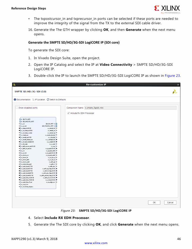
Reference Design Steps
XAPP1290 (v1.3) March 9, 2018 46www.xilinx.com
• The txpostcursor_in and txprecursor_in ports can be selected if these ports are needed to improve the integrity of the signal from the TX to the external SDI cable driver.
16. Generate the The GTH wrapper by clicking OK, and then Generate when the next menu opens.
Generate the SMPTE SD/HD/3G-SDI LogiCORE IP (SDI core)
To generate the SDI core:
1. In Vivado Design Suite, open the project.
2. Open the IP Catalog and select the IP at Video Connectivity > SMPTE SD/HD/3G-SDI LogiCORE IP.
3. Double-click the IP to launch the SMPTE SD/HD/3G-SDI LogiCORE IP as shown in Figure 23.
4. Select Include RX EDH Processor.
5. Generate the The SDI core by clicking OK, and click Generate when the next menu opens.
X-Ref Target - Figure 23
Figure 23: SMPTE SD/HD/3G-SDI LogiCORE IP
Reference Design Steps
XAPP1290 (v1.3) March 9, 2018 47www.xilinx.com
Instantiating the SDI Wrappers
There are two main SDI wrappers in the example SDI design, SDI wrapper support (kugth_3gsdi_wrapper_support.v) and SDI wrapper (kugth_3gsdi_wrapper.v), shown in Figure 5. SDI wrapper support is needed when QPLL0 and/or QPLL1 is/are used by the SDI wrapper and is instantiated only once per Quad.
SDI wrapper support and/or SDI wrapper must be instantiated and interconnected in a design. It is possible to implement the SDI interface without the SDI wrapper supplied with the example SDI design, but the wrapper reduces effort because it interconnects the SDI core, control module, and one channel of GT Wizard IP. If the wrapper is not used, the user must make these connections. The example SDI design provides an alternative SDI wrapper file, kugth_3gsdi_norxedh_wrapper.v that should be used when the SDI core is generated without the RX EDH processor.
The 6 wrappers that are included in the example SDI design are listed below. The example SDI design uses the wrappers highlighted in bold. Instantiation and usage depend entirely upon the SDI core configuration.
SDI 4-Channel wrapper per Quad
• kugth_3gsdi_4ch_wrapper.v
• kugth_3gsdi_norxedh_4ch_wrapper.v
SDI wrapper support
• kugth_3gsdi_wrapper_support.v
• kugth_3gsdi_norxedh_wrapper_support.v
SDI wrapper
• kugth_3gsdi_wrapper.v
• kugth_3gsdi_norxedh_wrapper.v
In addition to the wrappers instantiated by the SDI core, the SDI wrapper instances the these files:
• kugth_3gsdi_control.v
• kugth_3gsdi_drp_control.v
• kugth_3gsdi_drp_control_fsm.v
• kugth_3gsdi_rx_control.v
• kugth_3gsdi_tx_control.v
• sync_block.v
• smpte_3gsdi_rate_detect.v
• bs_flex_v_1.vhd
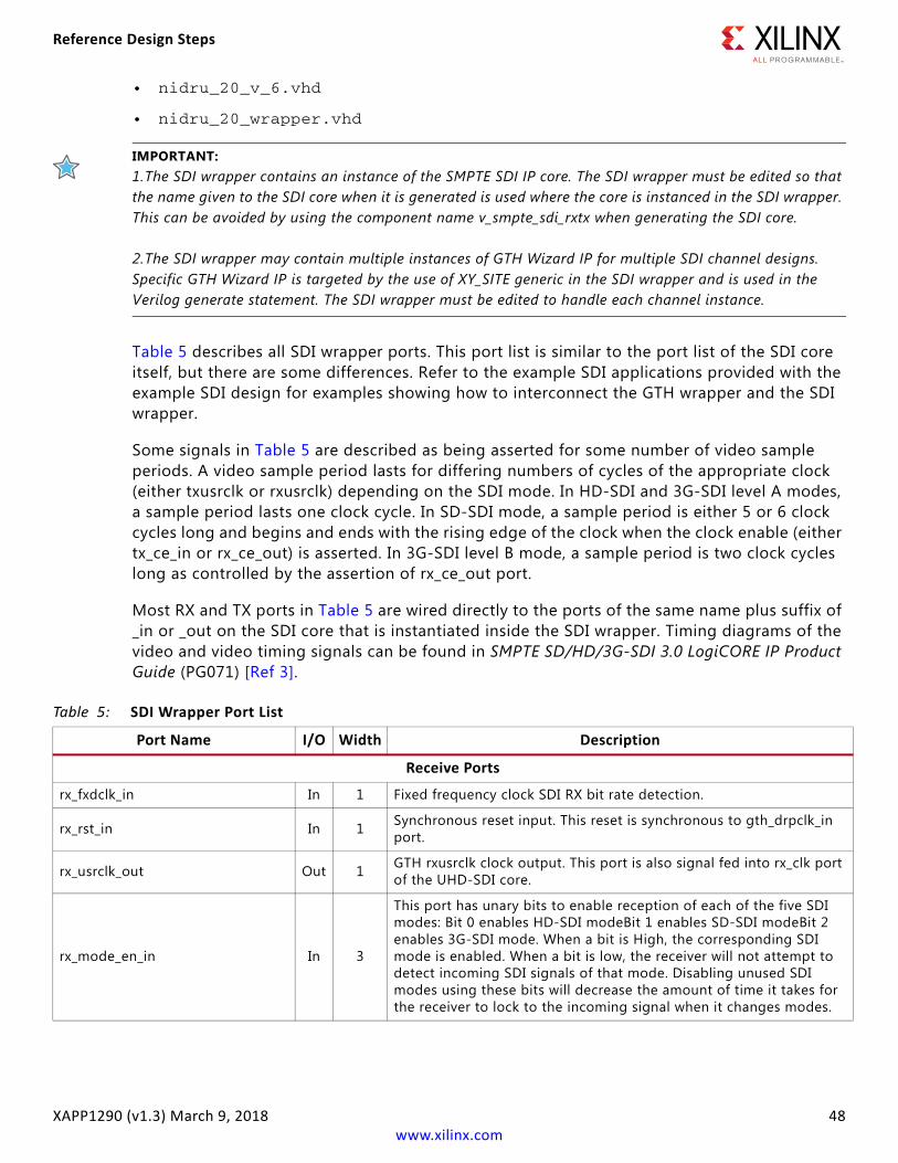
Reference Design Steps
XAPP1290 (v1.3) March 9, 2018 48www.xilinx.com
• nidru_20_v_6.vhd
• nidru_20_wrapper.vhd
IMPORTANT:1.The SDI wrapper contains an instance of the SMPTE SDI IP core. The SDI wrapper must be edited so that the name given to the SDI core when it is generated is used where the core is instanced in the SDI wrapper. This can be avoided by using the component name v_smpte_sdi_rxtx when generating the SDI core.
2.The SDI wrapper may contain multiple instances of GTH Wizard IP for multiple SDI channel designs. Specific GTH Wizard IP is targeted by the use of XY_SITE generic in the SDI wrapper and is used in the Verilog generate statement. The SDI wrapper must be edited to handle each channel instance.
Table 5 describes all SDI wrapper ports. This port list is similar to the port list of the SDI core itself, but there are some differences. Refer to the example SDI applications provided with the example SDI design for examples showing how to interconnect the GTH wrapper and the SDI wrapper.
Some signals in Table 5 are described as being asserted for some number of video sample periods. A video sample period lasts for differing numbers of cycles of the appropriate clock (either txusrclk or rxusrclk) depending on the SDI mode. In HD-SDI and 3G-SDI level A modes, a sample period lasts one clock cycle. In SD-SDI mode, a sample period is either 5 or 6 clock cycles long and begins and ends with the rising edge of the clock when the clock enable (either tx_ce_in or rx_ce_out) is asserted. In 3G-SDI level B mode, a sample period is two clock cycles long as controlled by the assertion of rx_ce_out port.
Most RX and TX ports in Table 5 are wired directly to the ports of the same name plus suffix of _in or _out on the SDI core that is instantiated inside the SDI wrapper. Timing diagrams of the video and video timing signals can be found in SMPTE SD/HD/3G-SDI 3.0 LogiCORE IP Product Guide (PG071) [Ref 3].
Table 5: SDI Wrapper Port List
Port Name I/O Width Description
Receive Ports
rx_fxdclk_in In 1 Fixed frequency clock SDI RX bit rate detection.
rx_rst_in In 1 Synchronous reset input. This reset is synchronous to gth_drpclk_in port.
rx_usrclk_out Out 1 GTH rxusrclk clock output. This port is also signal fed into rx_clk port of the UHD-SDI core.
rx_mode_en_in In 3
This port has unary bits to enable reception of each of the five SDI modes: Bit 0 enables HD-SDI modeBit 1 enables SD-SDI modeBit 2 enables 3G-SDI mode. When a bit is High, the corresponding SDI mode is enabled. When a bit is low, the receiver will not attempt to detect incoming SDI signals of that mode. Disabling unused SDI modes using these bits will decrease the amount of time it takes for the receiver to lock to the incoming signal when it changes modes.
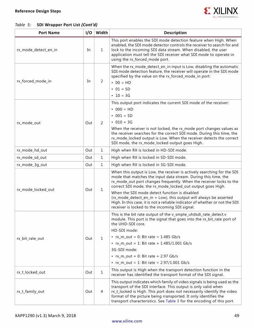
Reference Design Steps
XAPP1290 (v1.3) March 9, 2018 49www.xilinx.com
rx_mode_detect_en_in In 1
This port enables the SDI mode detection feature when High. When enabled, the SDI mode detector controls the receiver to search for and lock to the incoming SDI data stream. When disabled, the user application must tell the SDI receiver what SDI mode to operate in using the rx_forced_mode port.
rx_forced_mode_in In 2
When the rx_mode_detect_en_in input is Low, disabling the automatic SDI mode detection feature, the receiver will operate in the SDI mode specified by the value on the rx_forced_mode_in port:
• 00 = HD
• 01 = SD
• 10 = 3G
rx_mode_out Out 2
This output port indicates the current SDI mode of the receiver:
• 000 = HD
• 001 = SD
• 010 = 3G
When the receiver is not locked, the rx_mode port changes values as the receiver searches for the correct SDI mode. During this time, the rx_mode_locked output is Low. When the receiver detects the correct SDI mode, the rx_mode_locked output goes High.
rx_mode_hd_out Out 1 High when RX is locked in HD-SDI mode.
rx_mode_sd_out Out 1 High when RX is locked in SD-SDI mode.
rx_mode_3g_out Out 1 High when RX is locked in 3G-SDI mode.
rx_mode_locked_out Out 1
When this output is Low, the receiver is actively searching for the SDI mode that matches the input data stream. During this time, the rx_mode_out port changes frequently. When the receiver locks to the correct SDI mode, the rx_mode_locked_out output goes High.
When the SDI mode detect function is disabled (rx_mode_detect_en_in = Low), this output will always be asserted High. In this case, it is not a reliable indicator of whether or not the SDI receiver is locked to the incoming SDI signal.
rx_bit_rate_out Out 1
This is the bit rate output of the v_smpte_uhdsdi_rate_detect.v module. This port is the signal that goes into the rx_bit_rate port of the UHD-SDI core.
HD-SDI mode:
• rx_m_out = 0: Bit rate = 1.485 Gb/s
• rx_m_out = 1: Bit rate = 1.485/1.001 Gb/s
3G-SDI mode:
• rx_m_out = 0: Bit rate = 2.97 Gb/s
• rx_m_out = 1: Bit rate = 2.97/1.001 Gb/s
rx_t_locked_out Out 1 This output is High when the transport detection function in the receiver has identified the transport format of the SDI signal.
rx_t_family_out Out 4
This output indicates which family of video signals is being used as the transport of the SDI interface. This output is only valid when rx_t_locked is High. This port does not necessarily identify the video format of the picture being rransported. It only identifies the transport characteristics. See Table 3 for the encoding of this port.
Table 5: SDI Wrapper Port List (Cont’d)
Port Name I/O Width Description
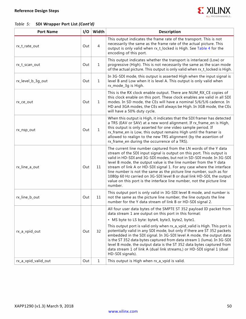
Reference Design Steps
XAPP1290 (v1.3) March 9, 2018 50www.xilinx.com
rx_t_rate_out Out 4
This output indicates the frame rate of the transport. This is not necessarily the same as the frame rate of the actual picture. This output is only valid when rx_t_locked is High. See Table 4 for the encoding of this port.
rx_t_scan_out Out 1This output indicates whether the transport is interlaced (Low) or progressive (High). This is not necessarily the same as the scan mode of the actual picture. This output is only valid when rx_t_locked is High.
rx_level_b_3g_out Out 1In 3G-SDI mode, this output is asserted High when the input signal is level B and Low when it is level A. This output is only valid when rx_mode_3g is High.
rx_ce_out Out 1
This is the RX clock enable output. There are NUM_RX_CE copies of this clock enable on this port. These clock enables are valid in all SDI modes. In SD mode, the CEs will have a nominal 5/6/5/6 cadence. In HD and 3GA modes, the CEs will always be High. In 3GB mode, the CEs will have a 50% duty cycle.
rx_nsp_out Out 1
When this output is High, it indicates that the SDI framer has detected a TRS (EAV or SAV) at a new word alignment. If rx_frame_en is High, this output is only asserted for one video sample period. If rx_frame_en is Low, this output remains High until the framer is allowed to realign to the new TRS alignment (by the assertion of rx_frame_en during the occurrence of a TRS).
rx_line_a_out Out 11
The current line number captured from the LN words of the Y data stream of the SDI input signal is output on this port. This output is valid in HD-SDI and 3G-SDI modes, but not in SD-SDI mode. In 3G-SDI level B mode, the output value is the line number from the Y data stream of link A or HD-SDI signal 1. For any case where the interface line number is not the same as the picture line number, such as for 1080p 60 Hz carried on 3G-SDI level B or dual link HD-SDI, the output value on this port is the interface line number, not the picture line number.
rx_line_b_out Out 11This output port is only valid in 3G-SDI level B mode, and number is not the same as the picture line number, the line outputs the line number for the Y data stream of link B or HD-SDI signal 2.
rx_a_vpid_out Out 32
All four user data bytes of the SMPTE ST 352 payload ID packet from data stream 1 are output on this port in this format:
• MS byte to LS byte: byte4, byte3, byte2, byte1.
This output port is valid only when rx_a_vpid_valid is High. This port is potentially valid in any SDI mode, but only if there are ST 352 packets embedded in the SDI signal. In 3G-SDI level A mode, the output data is the ST 352 data bytes captured from data stream 1 (luma). In 3G-SDI level B mode, the output data is the ST 352 data bytes captured from data stream 1 of link A (dual link streams,) or HD-SDI signal 1 (dual HD-SDI signals).
rx_a_vpid_valid_out Out 1 This output is High when rx_a_vpid is valid.
Table 5: SDI Wrapper Port List (Cont’d)
Port Name I/O Width Description
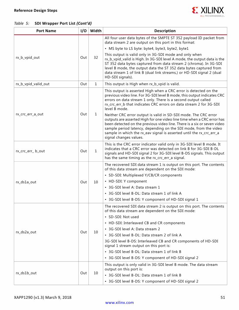
Reference Design Steps
XAPP1290 (v1.3) March 9, 2018 51www.xilinx.com
rx_b_vpid_out Out 32
All four user data bytes of the SMPTE ST 352 payload ID packet from data stream 2 are output on this port in this format:
• MS byte to LS byte: byte4, byte3, byte2, byte1
This output is valid only in 3G-SDI mode and only when rx_b_vpid_valid is High. In 3G-SDI level A mode, the output data is the ST 352 data bytes captured from data stream 2 (chroma). In 3G-SDI level B mode, the output data the ST 352 data bytes captured from data stream 1 of link B (dual link streams,) or HD-SDI signal 2 (dual HD-SDI signals).
rx_b_vpid_valid_out Out 1 This output is High when rx_b_vpid is valid.
rx_crc_err_a_out Out 1
This output is asserted High when a CRC error is detected on the previous video line. For 3G-SDI level B mode, this output indicates CRC errors on data stream 1 only. There is a second output called rx_crc_err_b that indicates CRC errors on data stream 2 for 3G-SDI level B mode.
Neither CRC error output is valid in SD-SDI mode. The CRC error outputs are asserted High for one video line time when a CRC error has been detected on the previous video line. There is a six or seven video sample period latency, depending on the SDI mode, from the video sample in which the rx_eav signal is asserted until the rx_crc_err_a signal changes values.
rx_crc_err_ b_out Out 1
This is the CRC error indicator valid only in 3G-SDI level B mode. It indicates that a CRC error was detected on link B for 3G-SDI B-DL signals and HD-SDI signal 2 for 3G-SDI level B-DS signals. This output has the same timing as the rx_crc_err_a signal.
rx_ds1a_out Out 10
The recovered SDI data stream 1 is output on this port. The contents of this data stream are dependent on the SDI mode:
• SD-SDI: Multiplexed Y/CB/CR components
• HD-SDI: Y component
• 3G-SDI level A: Data stream 1
• 3G-SDI level B-DL: Data stream 1 of link A
• 3G-SDI level B-DS: Y component of HD-SDI signal 1
rx_ds2a_out Out 10
The recovered SDI data stream 2 is output on this port. The contents of this data stream are dependent on the SDI mode:
• SD-SDI: Not used
• HD-SDI: Interleaved CB and CR components
• 3G-SDI level A: Data stream 2
• 3G-SDI level B-DL: Data stream 2 of link A
3G-SDI level B-DS: Interleaved CB and CR components of HD-SDI signal 1 stream output on this port is:
• 3G-SDI level B-DL: Data stream 1 of link B
• 3G-SDI level B-DS: Y component of HD-SDI signal 2
rx_ds1b_out Out 10
This output is only valid in 3G-SDI level B mode. The data stream output on this port is:
• 3G-SDI level B-DL: Data stream 1 of link B
• 3G-SDI level B-DS: Y component of HD-SDI signal 2
Table 5: SDI Wrapper Port List (Cont’d)
Port Name I/O Width Description
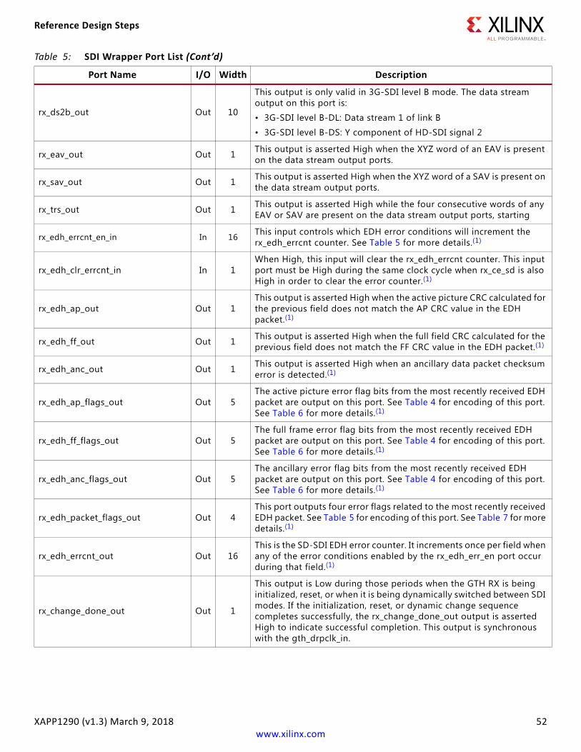
Reference Design Steps
XAPP1290 (v1.3) March 9, 2018 52www.xilinx.com
rx_ds2b_out Out 10
This output is only valid in 3G-SDI level B mode. The data stream output on this port is:
• 3G-SDI level B-DL: Data stream 1 of link B
• 3G-SDI level B-DS: Y component of HD-SDI signal 2
rx_eav_out Out 1 This output is asserted High when the XYZ word of an EAV is present on the data stream output ports.
rx_sav_out Out 1 This output is asserted High when the XYZ word of a SAV is present on the data stream output ports.
rx_trs_out Out 1 This output is asserted High while the four consecutive words of any EAV or SAV are present on the data stream output ports, starting
rx_edh_errcnt_en_in In 16 This input controls which EDH error conditions will increment the rx_edh_errcnt counter. See Table 5 for more details.(1)
rx_edh_clr_errcnt_in In 1When High, this input will clear the rx_edh_errcnt counter. This input port must be High during the same clock cycle when rx_ce_sd is also High in order to clear the error counter.(1)
rx_edh_ap_out Out 1This output is asserted High when the active picture CRC calculated for the previous field does not match the AP CRC value in the EDH packet.(1)
rx_edh_ff_out Out 1 This output is asserted High when the full field CRC calculated for the previous field does not match the FF CRC value in the EDH packet.(1)
rx_edh_anc_out Out 1 This output is asserted High when an ancillary data packet checksum error is detected.(1)
rx_edh_ap_flags_out Out 5The active picture error flag bits from the most recently received EDH packet are output on this port. See Table 4 for encoding of this port. See Table 6 for more details.(1)
rx_edh_ff_flags_out Out 5The full frame error flag bits from the most recently received EDH packet are output on this port. See Table 4 for encoding of this port. See Table 6 for more details.(1)
rx_edh_anc_flags_out Out 5The ancillary error flag bits from the most recently received EDH packet are output on this port. See Table 4 for encoding of this port. See Table 6 for more details.(1)
rx_edh_packet_flags_out Out 4This port outputs four error flags related to the most recently received EDH packet. See Table 5 for encoding of this port. See Table 7 for more details.(1)
rx_edh_errcnt_out Out 16This is the SD-SDI EDH error counter. It increments once per field when any of the error conditions enabled by the rx_edh_err_en port occur during that field.(1)
rx_change_done_out Out 1
This output is Low during those periods when the GTH RX is being initialized, reset, or when it is being dynamically switched between SDI modes. If the initialization, reset, or dynamic change sequence completes successfully, the rx_change_done_out output is asserted High to indicate successful completion. This output is synchronous with the gth_drpclk_in.
Table 5: SDI Wrapper Port List (Cont’d)
Port Name I/O Width Description
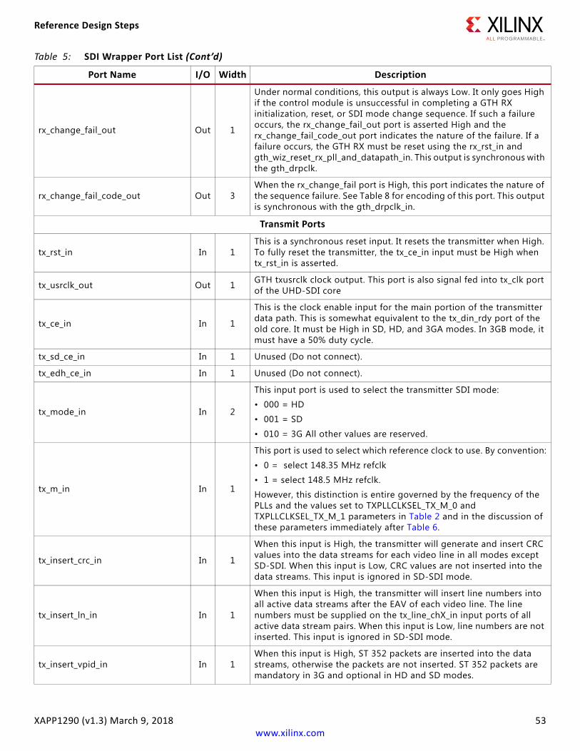
Reference Design Steps
XAPP1290 (v1.3) March 9, 2018 53www.xilinx.com
rx_change_fail_out Out 1
Under normal conditions, this output is always Low. It only goes High if the control module is unsuccessful in completing a GTH RX initialization, reset, or SDI mode change sequence. If such a failure occurs, the rx_change_fail_out port is asserted High and the rx_change_fail_code_out port indicates the nature of the failure. If a failure occurs, the GTH RX must be reset using the rx_rst_in and gth_wiz_reset_rx_pll_and_datapath_in. This output is synchronous with the gth_drpclk.
rx_change_fail_code_out Out 3When the rx_change_fail port is High, this port indicates the nature of the sequence failure. See Table 8 for encoding of this port. This output is synchronous with the gth_drpclk_in.
Transmit Ports
tx_rst_in In 1This is a synchronous reset input. It resets the transmitter when High. To fully reset the transmitter, the tx_ce_in input must be High when tx_rst_in is asserted.
tx_usrclk_out Out 1 GTH txusrclk clock output. This port is also signal fed into tx_clk port of the UHD-SDI core
tx_ce_in In 1
This is the clock enable input for the main portion of the transmitter data path. This is somewhat equivalent to the tx_din_rdy port of the old core. It must be High in SD, HD, and 3GA modes. In 3GB mode, it must have a 50% duty cycle.
tx_sd_ce_in In 1 Unused (Do not connect).
tx_edh_ce_in In 1 Unused (Do not connect).
tx_mode_in In 2
This input port is used to select the transmitter SDI mode:
• 000 = HD
• 001 = SD
• 010 = 3G All other values are reserved.
tx_m_in In 1
This port is used to select which reference clock to use. By convention:
• 0 = select 148.35 MHz refclk
• 1 = select 148.5 MHz refclk.
However, this distinction is entire governed by the frequency of the PLLs and the values set to TXPLLCLKSEL_TX_M_0 and TXPLLCLKSEL_TX_M_1 parameters in Table 2 and in the discussion of these parameters immediately after Table 6.
tx_insert_crc_in In 1
When this input is High, the transmitter will generate and insert CRC values into the data streams for each video line in all modes except SD-SDI. When this input is Low, CRC values are not inserted into the data streams. This input is ignored in SD-SDI mode.
tx_insert_ln_in In 1
When this input is High, the transmitter will insert line numbers into all active data streams after the EAV of each video line. The line numbers must be supplied on the tx_line_chX_in input ports of all active data stream pairs. When this input is Low, line numbers are not inserted. This input is ignored in SD-SDI mode.
tx_insert_vpid_in In 1When this input is High, ST 352 packets are inserted into the data streams, otherwise the packets are not inserted. ST 352 packets are mandatory in 3G and optional in HD and SD modes.
Table 5: SDI Wrapper Port List (Cont’d)
Port Name I/O Width Description
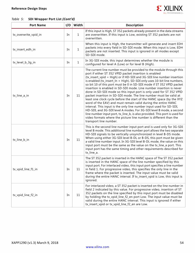
Reference Design Steps
XAPP1290 (v1.3) March 9, 2018 54www.xilinx.com
tx_overwrite_vpid_in In 1If this input is High, ST 352 packets already present in the data streams are overwritten. If this input is Low, existing ST 352 packets are not overwritten.
tx_insert_edh_in In 1
When this input is High, the transmitter will generate and insert EDH packets into every field in SD-SDI mode. When this input is Low, EDH packets are not inserted. This input is ignored in all modes except SD-SDI mode.
tx_level_b_3g_in In 1 In 3G-SDI mode, this input determines whether the module is configured for level A (Low) or for level B (High).
tx_line_a_in In 11
The current line number must be provided to the module through this port if either ST 352 VPID packet insertion is enabled (tx_insert_vpid = High) or if HD-SDI and 3G-SDI line number insertion is enabled (tx_insert_ln = High). SD-SDI only uses 10-bit line numbers, so bit 10 of this port must be 0 in SD-SDI mode if ST 352 VPID packet insertion is enabled in SD-SDI mode. Line number insertion is never done in SD-SDI mode so this input port is only used for ST 352 VPID packet insertion in SD-SDI mode. The line number must be valid at least one clock cycle before the start of the HANC space (by the XYZ word of the EAV) and must remain valid during the entire HANC interval. This input is the only line number input used for SD-SDI, HD-SDI, and 3G-SDI level A modes. For 3G-SDI level B mode, a second line number input port, tx_line_b, is also provided. This port is used for video formats where the picture line number is different than the transport line number.
tx_line_b_in In 11
This is the second line number input port and is used only for 3G-SDI level B mode. This additional line number port allows the two separate HD-SDI signals to be vertically unsynchronized in level B-DS mode. When using either 3G-SDI level B-DL or B-DS, this port must be given a valid line number input. In 3G-SDI level B-DL mode, the value on this input port must be the same as the value on the tx_line_a port. This input port has the same timing and other requirements described for tx_line_a.
tx_vpid_line_f1_in In 11
The ST 352 packet is inserted in the HANC space of The ST 352 packet is inserted in the HANC space of the line number specified by this input port. For interlaced video, this input port specifies a line number in field 1. For progressive video, this specifies the only line in the frame where the packet is inserted. The input value must be valid during the entire HANC interval. If tx_insert_vpid is Low, this input is ignored.
tx_vpid_line_f2_in In 11
For interlaced video, a ST 352 packet is inserted on the line number in field 2 indicated by this value. For progressive video, insertion of ST 352 packets on the line specified by this input port must be disabled by holding the tx_vpid_line_f2_en port Low. The input value must be valid during the entire HANC interval. This input is ignored if either tx_insert_vpid or tx_vpid_line_f2_en are Low.
Table 5: SDI Wrapper Port List (Cont’d)
Port Name I/O Width Description
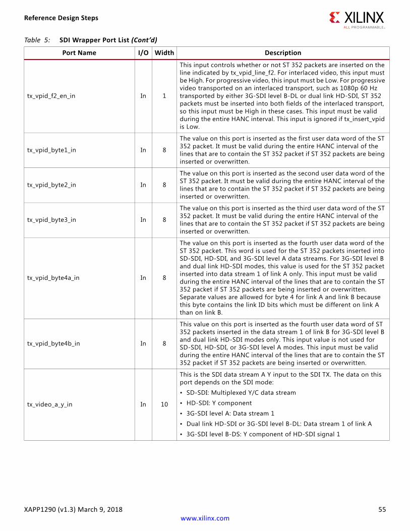
Reference Design Steps
XAPP1290 (v1.3) March 9, 2018 55www.xilinx.com
tx_vpid_f2_en_in In 1
This input controls whether or not ST 352 packets are inserted on the line indicated by tx_vpid_line_f2. For interlaced video, this input must be High. For progressive video, this input must be Low. For progressive video transported on an interlaced transport, such as 1080p 60 Hz transported by either 3G-SDI level B-DL or dual link HD-SDI, ST 352 packets must be inserted into both fields of the interlaced transport, so this input must be High in these cases. This input must be valid during the entire HANC interval. This input is ignored if tx_insert_vpid is Low.
tx_vpid_byte1_in In 8
The value on this port is inserted as the first user data word of the ST 352 packet. It must be valid during the entire HANC interval of the lines that are to contain the ST 352 packet if ST 352 packets are being inserted or overwritten.
tx_vpid_byte2_in In 8
The value on this port is inserted as the second user data word of the ST 352 packet. It must be valid during the entire HANC interval of the lines that are to contain the ST 352 packet if ST 352 packets are being inserted or overwritten.
tx_vpid_byte3_in In 8
The value on this port is inserted as the third user data word of the ST 352 packet. It must be valid during the entire HANC interval of the lines that are to contain the ST 352 packet if ST 352 packets are being inserted or overwritten.
tx_vpid_byte4a_in In 8
The value on this port is inserted as the fourth user data word of the ST 352 packet. This word is used for the ST 352 packets inserted into SD-SDI, HD-SDI, and 3G-SDI level A data streams. For 3G-SDI level B and dual link HD-SDI modes, this value is used for the ST 352 packet inserted into data stream 1 of link A only. This input must be valid during the entire HANC interval of the lines that are to contain the ST 352 packet if ST 352 packets are being inserted or overwritten. Separate values are allowed for byte 4 for link A and link B because this byte contains the link ID bits which must be different on link A than on link B.
tx_vpid_byte4b_in In 8
This value on this port is inserted as the fourth user data word of ST 352 packets inserted in the data stream 1 of link B for 3G-SDI level B and dual link HD-SDI modes only. This input value is not used for SD-SDI, HD-SDI, or 3G-SDI level A modes. This input must be valid during the entire HANC interval of the lines that are to contain the ST 352 packet if ST 352 packets are being inserted or overwritten.
tx_video_a_y_in In 10
This is the SDI data stream A Y input to the SDI TX. The data on this port depends on the SDI mode:
• SD-SDI: Multiplexed Y/C data stream
• HD-SDI: Y component
• 3G-SDI level A: Data stream 1
• Dual link HD-SDI or 3G-SDI level B-DL: Data stream 1 of link A
• 3G-SDI level B-DS: Y component of HD-SDI signal 1
Table 5: SDI Wrapper Port List (Cont’d)
Port Name I/O Width Description
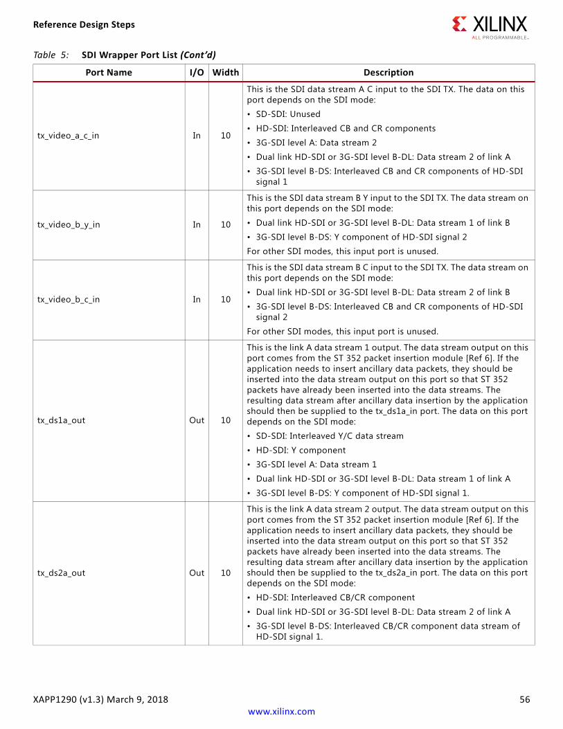
Reference Design Steps
XAPP1290 (v1.3) March 9, 2018 56www.xilinx.com
tx_video_a_c_in In 10
This is the SDI data stream A C input to the SDI TX. The data on this port depends on the SDI mode:
• SD-SDI: Unused
• HD-SDI: Interleaved CB and CR components
• 3G-SDI level A: Data stream 2
• Dual link HD-SDI or 3G-SDI level B-DL: Data stream 2 of link A
• 3G-SDI level B-DS: Interleaved CB and CR components of HD-SDI signal 1
tx_video_b_y_in In 10
This is the SDI data stream B Y input to the SDI TX. The data stream on this port depends on the SDI mode:
• Dual link HD-SDI or 3G-SDI level B-DL: Data stream 1 of link B
• 3G-SDI level B-DS: Y component of HD-SDI signal 2
For other SDI modes, this input port is unused.
tx_video_b_c_in In 10
This is the SDI data stream B C input to the SDI TX. The data stream on this port depends on the SDI mode:
• Dual link HD-SDI or 3G-SDI level B-DL: Data stream 2 of link B
• 3G-SDI level B-DS: Interleaved CB and CR components of HD-SDI signal 2
For other SDI modes, this input port is unused.
tx_ds1a_out Out 10
This is the link A data stream 1 output. The data stream output on this port comes from the ST 352 packet insertion module [Ref 6]. If the application needs to insert ancillary data packets, they should be inserted into the data stream output on this port so that ST 352 packets have already been inserted into the data streams. The resulting data stream after ancillary data insertion by the application should then be supplied to the tx_ds1a_in port. The data on this port depends on the SDI mode:
• SD-SDI: Interleaved Y/C data stream
• HD-SDI: Y component
• 3G-SDI level A: Data stream 1
• Dual link HD-SDI or 3G-SDI level B-DL: Data stream 1 of link A
• 3G-SDI level B-DS: Y component of HD-SDI signal 1.
tx_ds2a_out Out 10
This is the link A data stream 2 output. The data stream output on this port comes from the ST 352 packet insertion module [Ref 6]. If the application needs to insert ancillary data packets, they should be inserted into the data stream output on this port so that ST 352 packets have already been inserted into the data streams. The resulting data stream after ancillary data insertion by the application should then be supplied to the tx_ds2a_in port. The data on this port depends on the SDI mode:
• HD-SDI: Interleaved CB/CR component
• Dual link HD-SDI or 3G-SDI level B-DL: Data stream 2 of link A
• 3G-SDI level B-DS: Interleaved CB/CR component data stream of HD-SDI signal 1.
Table 5: SDI Wrapper Port List (Cont’d)
Port Name I/O Width Description
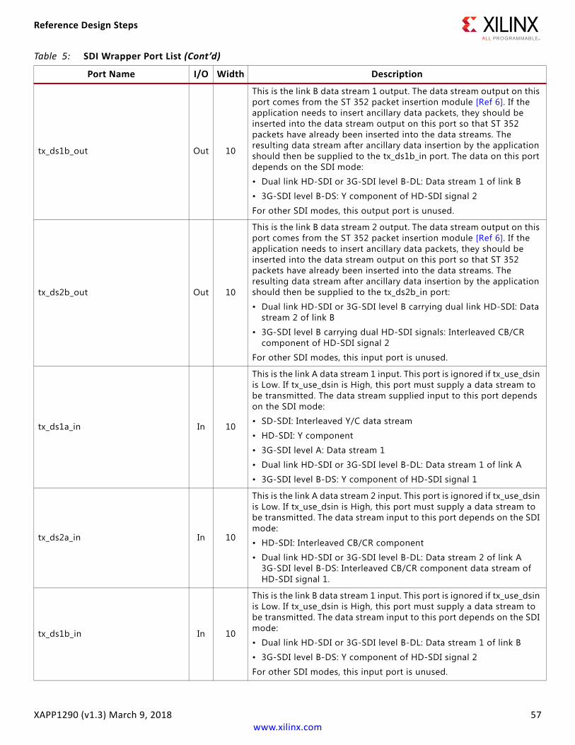
Reference Design Steps
XAPP1290 (v1.3) March 9, 2018 57www.xilinx.com
tx_ds1b_out Out 10
This is the link B data stream 1 output. The data stream output on this port comes from the ST 352 packet insertion module [Ref 6]. If the application needs to insert ancillary data packets, they should be inserted into the data stream output on this port so that ST 352 packets have already been inserted into the data streams. The resulting data stream after ancillary data insertion by the application should then be supplied to the tx_ds1b_in port. The data on this port depends on the SDI mode:
• Dual link HD-SDI or 3G-SDI level B-DL: Data stream 1 of link B
• 3G-SDI level B-DS: Y component of HD-SDI signal 2
For other SDI modes, this output port is unused.
tx_ds2b_out Out 10
This is the link B data stream 2 output. The data stream output on this port comes from the ST 352 packet insertion module [Ref 6]. If the application needs to insert ancillary data packets, they should be inserted into the data stream output on this port so that ST 352 packets have already been inserted into the data streams. The resulting data stream after ancillary data insertion by the application should then be supplied to the tx_ds2b_in port:
• Dual link HD-SDI or 3G-SDI level B carrying dual link HD-SDI: Data stream 2 of link B
• 3G-SDI level B carrying dual HD-SDI signals: Interleaved CB/CR component of HD-SDI signal 2
For other SDI modes, this input port is unused.
tx_ds1a_in In 10
This is the link A data stream 1 input. This port is ignored if tx_use_dsin is Low. If tx_use_dsin is High, this port must supply a data stream to be transmitted. The data stream supplied input to this port depends on the SDI mode:
• SD-SDI: Interleaved Y/C data stream
• HD-SDI: Y component
• 3G-SDI level A: Data stream 1
• Dual link HD-SDI or 3G-SDI level B-DL: Data stream 1 of link A
• 3G-SDI level B-DS: Y component of HD-SDI signal 1
tx_ds2a_in In 10
This is the link A data stream 2 input. This port is ignored if tx_use_dsin is Low. If tx_use_dsin is High, this port must supply a data stream to be transmitted. The data stream input to this port depends on the SDI mode:
• HD-SDI: Interleaved CB/CR component
• Dual link HD-SDI or 3G-SDI level B-DL: Data stream 2 of link A 3G-SDI level B-DS: Interleaved CB/CR component data stream of HD-SDI signal 1.
tx_ds1b_in In 10
This is the link B data stream 1 input. This port is ignored if tx_use_dsin is Low. If tx_use_dsin is High, this port must supply a data stream to be transmitted. The data stream input to this port depends on the SDI mode:
• Dual link HD-SDI or 3G-SDI level B-DL: Data stream 1 of link B
• 3G-SDI level B-DS: Y component of HD-SDI signal 2
For other SDI modes, this input port is unused.
Table 5: SDI Wrapper Port List (Cont’d)
Port Name I/O Width Description
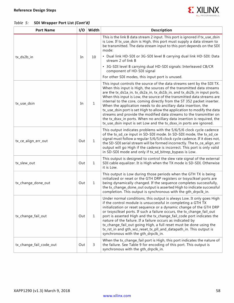
Reference Design Steps
XAPP1290 (v1.3) March 9, 2018 58www.xilinx.com
tx_ds2b_in In 10
This is the link B data stream 2 input. This port is ignored if tx_use_dsin is Low. If tx_use_dsin is High, this port must supply a data stream to be transmitted. The data stream input to this port depends on the SDI mode:
• Dual link HD-SDI or 3G-SDI level B carrying dual link HD-SDI: Data stream 2 of link B
• 3G-SDI level B carrying dual HD-SDI signals: Interleaved CB/CR component of HD-SDI signal
For other SDI modes, this input port is unused.
tx_use_dsin In 1
This input controls the source of the data streams sent by the SDI TX. When this input is High, the sources of the transmitted data streams are the tx_ds1a_in, tx_ds2a_in, tx_ds1b_in, and tx_ds2b_in input ports. When this input is Low, the source of the transmitted data streams are internal to the core, coming directly from the ST 352 packet inserter. When the application needs to do ancillary data insertion, the tx_use_dsin port is set High to allow the application to modify the data streams and provide the modified data streams to the transmitter on the tx_dsxx_in ports. When no ancillary data insertion is required, the tx_use_dsin input is set Low and the tx_dsxx_in ports are ignored.
tx_ce_align_err_out Out 1
This output indicates problems with the 5/6/5/6 clock cycle cadence of the tx_sd_ce input in SD-SDI mode. In SD-SDI mode, the tx_sd_ce signal must follow a regular 5/6/5/6 clock cycle cadence. If it does not, the SD-SDI serial stream will be formed incorrectly. The tx_ce_align_err output will go High if the cadence is incorrect. This port is only valid in SD-SDI mode and only if tx_sd_bitrep_bypass is Low.
tx_slew_out Out 1This output is designed to control the slew rate signal of the external SDI cable equalizer. It is High when the TX mode is SD-SDI. Otherwise it is Low.
tx_change_done_out Out 1
This output is Low during those periods when the GTH TX is being initialized or reset or the GTH DRP registers or txsysclksel ports are being dynamically changed. If the sequence completes successfully, the tx_change_done_out output is asserted High to indicate successful completion. This output is synchronous with the gth_drpclk_in.
tx_change_fail_out Out 1
Under normal conditions, this output is always Low. It only goes High if the control module is unsuccessful in completing a GTH TX initialization or reset sequence or a dynamic change of the GTH DRP or txsysclksel ports. If such a failure occurs, the tx_change_fail_out port is asserted High and the tx_change_fail_code port indicates the nature of the failure. If a failure occurs as indicated by tx_change_fail_out going High, a full reset must be done using the tx_rst_in and gth_wiz_reset_tx_pll_and_datapath_in. This output is synchronous with the gth_drpclk_in.
tx_change_fail_code_out Out 3When the tx_change_fail port is High, this port indicates the nature of the failure. See Table 9 for encoding of this port. This output is synchronous with the gth_drpclk_in.
Table 5: SDI Wrapper Port List (Cont’d)
Port Name I/O Width Description
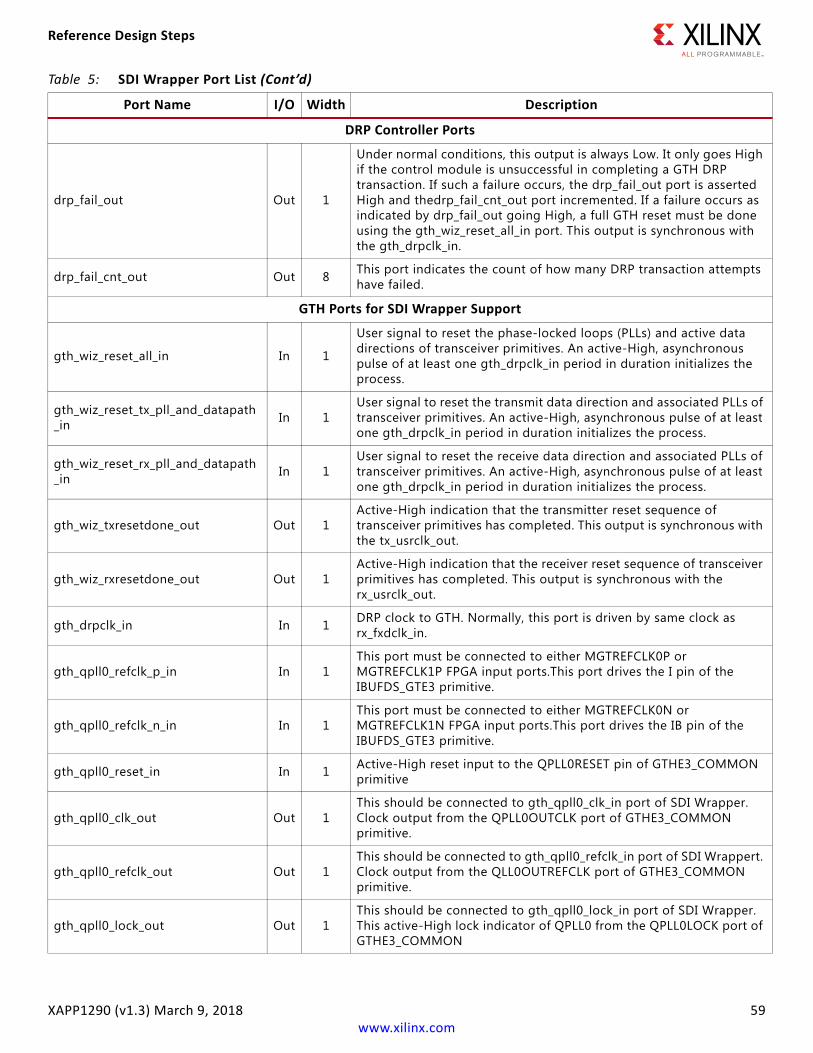
Reference Design Steps
XAPP1290 (v1.3) March 9, 2018 59www.xilinx.com
DRP Controller Ports
drp_fail_out Out 1
Under normal conditions, this output is always Low. It only goes High if the control module is unsuccessful in completing a GTH DRP transaction. If such a failure occurs, the drp_fail_out port is asserted High and thedrp_fail_cnt_out port incremented. If a failure occurs as indicated by drp_fail_out going High, a full GTH reset must be done using the gth_wiz_reset_all_in port. This output is synchronous with the gth_drpclk_in.
drp_fail_cnt_out Out 8 This port indicates the count of how many DRP transaction attempts have failed.
GTH Ports for SDI Wrapper Support
gth_wiz_reset_all_in In 1
User signal to reset the phase-locked loops (PLLs) and active data directions of transceiver primitives. An active-High, asynchronous pulse of at least one gth_drpclk_in period in duration initializes the process.
gth_wiz_reset_tx_pll_and_datapath_in In 1
User signal to reset the transmit data direction and associated PLLs of transceiver primitives. An active-High, asynchronous pulse of at least one gth_drpclk_in period in duration initializes the process.
gth_wiz_reset_rx_pll_and_datapath_in In 1
User signal to reset the receive data direction and associated PLLs of transceiver primitives. An active-High, asynchronous pulse of at least one gth_drpclk_in period in duration initializes the process.
gth_wiz_txresetdone_out Out 1Active-High indication that the transmitter reset sequence of transceiver primitives has completed. This output is synchronous with the tx_usrclk_out.
gth_wiz_rxresetdone_out Out 1Active-High indication that the receiver reset sequence of transceiver primitives has completed. This output is synchronous with the rx_usrclk_out.
gth_drpclk_in In 1 DRP clock to GTH. Normally, this port is driven by same clock as rx_fxdclk_in.
gth_qpll0_refclk_p_in In 1This port must be connected to either MGTREFCLK0P or MGTREFCLK1P FPGA input ports.This port drives the I pin of the IBUFDS_GTE3 primitive.
gth_qpll0_refclk_n_in In 1This port must be connected to either MGTREFCLK0N or MGTREFCLK1N FPGA input ports.This port drives the IB pin of the IBUFDS_GTE3 primitive.
gth_qpll0_reset_in In 1 Active-High reset input to the QPLL0RESET pin of GTHE3_COMMON primitive
gth_qpll0_clk_out Out 1This should be connected to gth_qpll0_clk_in port of SDI Wrapper. Clock output from the QPLL0OUTCLK port of GTHE3_COMMON primitive.
gth_qpll0_refclk_out Out 1This should be connected to gth_qpll0_refclk_in port of SDI Wrappert. Clock output from the QLL0OUTREFCLK port of GTHE3_COMMON primitive.
gth_qpll0_lock_out Out 1This should be connected to gth_qpll0_lock_in port of SDI Wrapper. This active-High lock indicator of QPLL0 from the QPLL0LOCK port of GTHE3_COMMON
Table 5: SDI Wrapper Port List (Cont’d)
Port Name I/O Width Description
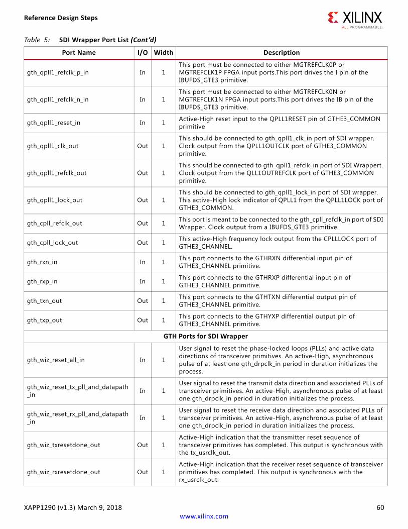
Reference Design Steps
XAPP1290 (v1.3) March 9, 2018 60www.xilinx.com
gth_qpll1_refclk_p_in In 1This port must be connected to either MGTREFCLK0P or MGTREFCLK1P FPGA input ports.This port drives the I pin of the IBUFDS_GTE3 primitive.
gth_qpll1_refclk_n_in In 1This port must be connected to either MGTREFCLK0N or MGTREFCLK1N FPGA input ports.This port drives the IB pin of the IBUFDS_GTE3 primitive.
gth_qpll1_reset_in In 1 Active-High reset input to the QPLL1RESET pin of GTHE3_COMMON primitive
gth_qpll1_clk_out Out 1This should be connected to gth_qpll1_clk_in port of SDI wrapper. Clock output from the QPLL1OUTCLK port of GTHE3_COMMON primitive.
gth_qpll1_refclk_out Out 1This should be connected to gth_qpll1_refclk_in port of SDI Wrappert. Clock output from the QLL1OUTREFCLK port of GTHE3_COMMON primitive.
gth_qpll1_lock_out Out 1This should be connected to gth_qpll1_lock_in port of SDI wrapper. This active-High lock indicator of QPLL1 from the QPLL1LOCK port of GTHE3_COMMON.
gth_cpll_refclk_out Out 1 This port is meant to be connected to the gth_cpll_refclk_in port of SDI Wrapper. Clock output from a IBUFDS_GTE3 primitive.
gth_cpll_lock_out Out 1 This active-High frequency lock output from the CPLLLOCK port of GTHE3_CHANNEL.
gth_rxn_in In 1 This port connects to the GTHRXN differential input pin of GTHE3_CHANNEL primitive.
gth_rxp_in In 1 This port connects to the GTHRXP differential input pin of GTHE3_CHANNEL primitive.
gth_txn_out Out 1 This port connects to the GTHTXN differential output pin of GTHE3_CHANNEL primitive.
gth_txp_out Out 1 This port connects to the GTHYXP differential output pin of GTHE3_CHANNEL primitive.
GTH Ports for SDI Wrapper
gth_wiz_reset_all_in In 1
User signal to reset the phase-locked loops (PLLs) and active data directions of transceiver primitives. An active-High, asynchronous pulse of at least one gth_drpclk_in period in duration initializes the process.
gth_wiz_reset_tx_pll_and_datapath_in In 1
User signal to reset the transmit data direction and associated PLLs of transceiver primitives. An active-High, asynchronous pulse of at least one gth_drpclk_in period in duration initializes the process.
gth_wiz_reset_rx_pll_and_datapath_in In 1
User signal to reset the receive data direction and associated PLLs of transceiver primitives. An active-High, asynchronous pulse of at least one gth_drpclk_in period in duration initializes the process.
gth_wiz_txresetdone_out Out 1Active-High indication that the transmitter reset sequence of transceiver primitives has completed. This output is synchronous with the tx_usrclk_out.
gth_wiz_rxresetdone_out Out 1Active-High indication that the receiver reset sequence of transceiver primitives has completed. This output is synchronous with the rx_usrclk_out.
Table 5: SDI Wrapper Port List (Cont’d)
Port Name I/O Width Description
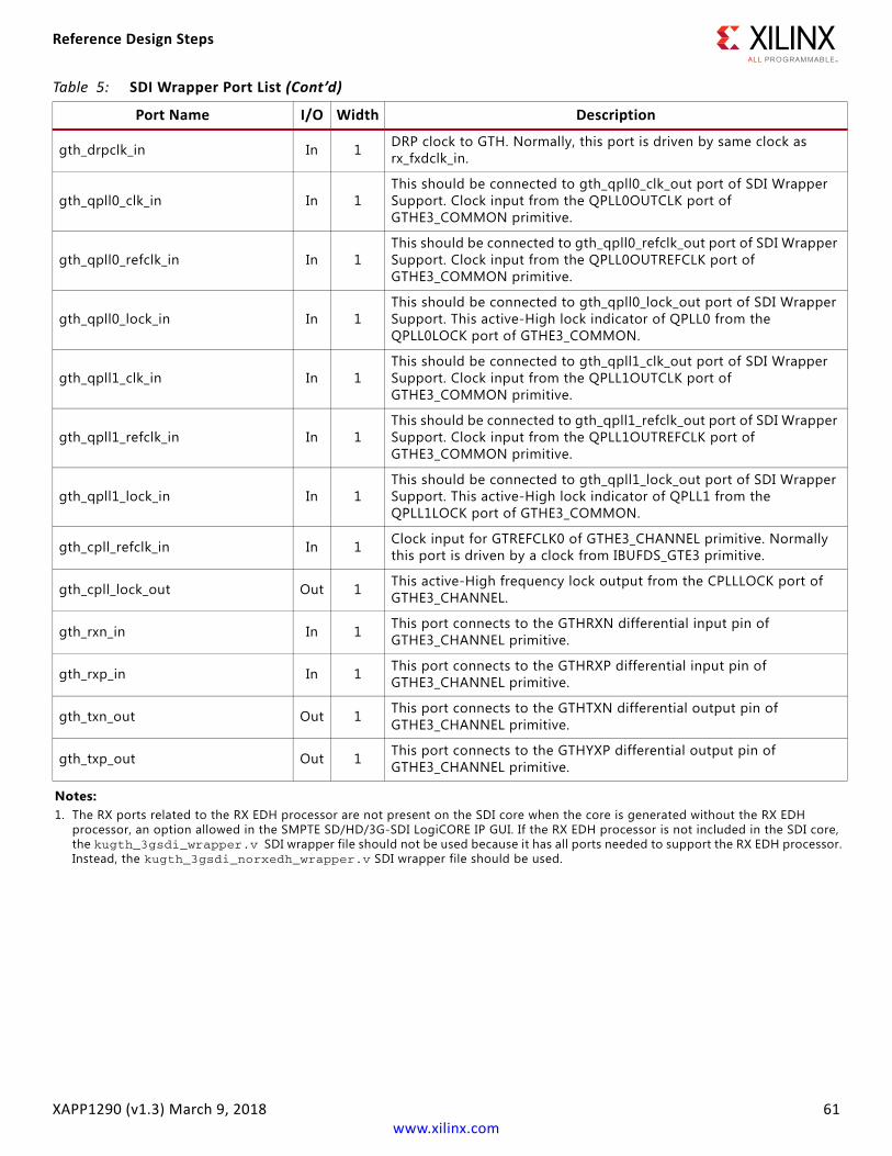
Reference Design Steps
XAPP1290 (v1.3) March 9, 2018 61www.xilinx.com
gth_drpclk_in In 1 DRP clock to GTH. Normally, this port is driven by same clock as rx_fxdclk_in.
gth_qpll0_clk_in In 1This should be connected to gth_qpll0_clk_out port of SDI Wrapper Support. Clock input from the QPLL0OUTCLK port of GTHE3_COMMON primitive.
gth_qpll0_refclk_in In 1This should be connected to gth_qpll0_refclk_out port of SDI Wrapper Support. Clock input from the QPLL0OUTREFCLK port of GTHE3_COMMON primitive.
gth_qpll0_lock_in In 1This should be connected to gth_qpll0_lock_out port of SDI Wrapper Support. This active-High lock indicator of QPLL0 from the QPLL0LOCK port of GTHE3_COMMON.
gth_qpll1_clk_in In 1This should be connected to gth_qpll1_clk_out port of SDI Wrapper Support. Clock input from the QPLL1OUTCLK port of GTHE3_COMMON primitive.
gth_qpll1_refclk_in In 1This should be connected to gth_qpll1_refclk_out port of SDI Wrapper Support. Clock input from the QPLL1OUTREFCLK port of GTHE3_COMMON primitive.
gth_qpll1_lock_in In 1This should be connected to gth_qpll1_lock_out port of SDI Wrapper Support. This active-High lock indicator of QPLL1 from the QPLL1LOCK port of GTHE3_COMMON.
gth_cpll_refclk_in In 1 Clock input for GTREFCLK0 of GTHE3_CHANNEL primitive. Normally this port is driven by a clock from IBUFDS_GTE3 primitive.
gth_cpll_lock_out Out 1 This active-High frequency lock output from the CPLLLOCK port of GTHE3_CHANNEL.
gth_rxn_in In 1 This port connects to the GTHRXN differential input pin of GTHE3_CHANNEL primitive.
gth_rxp_in In 1 This port connects to the GTHRXP differential input pin of GTHE3_CHANNEL primitive.
gth_txn_out Out 1 This port connects to the GTHTXN differential output pin of GTHE3_CHANNEL primitive.
gth_txp_out Out 1 This port connects to the GTHYXP differential output pin of GTHE3_CHANNEL primitive.
Notes: 1. The RX ports related to the RX EDH processor are not present on the SDI core when the core is generated without the RX EDH
processor, an option allowed in the SMPTE SD/HD/3G-SDI LogiCORE IP GUI. If the RX EDH processor is not included in the SDI core, the kugth_3gsdi_wrapper.v SDI wrapper file should not be used because it has all ports needed to support the RX EDH processor. Instead, the kugth_3gsdi_norxedh_wrapper.v SDI wrapper file should be used.
Table 5: SDI Wrapper Port List (Cont’d)
Port Name I/O Width Description
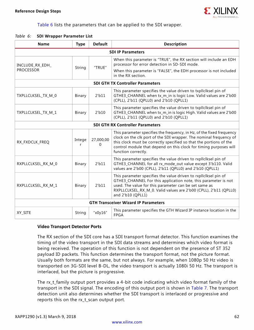
Reference Design Steps
XAPP1290 (v1.3) March 9, 2018 62www.xilinx.com
Table 6 lists the parameters that can be applied to the SDI wrapper.
Video Transport Detector Ports
The RX section of the SDI core has a SDI transport format detector. This function examines the timing of the video transport in the SDI data streams and determines which video format is being received. The operation of this function is not dependent on the presence of ST 352 payload ID packets. This function determines the transport format, not the picture format. Usually both formats are the same, but not always. For example, when 1080p 50 Hz video is transported on 3G-SDI level B-DL, the video transport is actually 1080i 50 Hz. The transport is interlaced, but the picture is progressive.
The rx_t_family output port provides a 4-bit code indicating which video format family of the transport in the SDI signal. The encoding of this output port is shown in Table 7. The transport detection unit also determines whether the SDI transport is interlaced or progressive and reports this on the rx_t_scan output port.
Table 6: SDI Wrapper Parameter List
Name Type Default Description
SDI IP Parameters
INCLUDE_RX_EDH_PROCESSOR String “TRUE”
When this parameter is “TRUE”, the RX section will include an EDH processor for error detection in SD-SDI mode.
When this parameter is “FALSE”, the EDH processor is not included in the RX section.
SDI GTH TX Controller Parameters
TXPLLCLKSEL_TX_M_0 Binary 2'b11This parameter specifies the value driven to txpllclksel pin of GTHE3_CHANNEL when tx_m_in is logic Low. Valid values are 2'b00 (CPLL), 2'b11 (QPLL0) and 2'b10 (QPLL1)
TXPLLCLKSEL_TX_M_1 Binary 2'b10This parameter specifies the value driven to txpllclksel pin of GTHE3_CHANNEL when tx_m_in is logic High. Valid values are 2'b00 (CPLL), 2'b11 (QPLL0) and 2'b10 (QPLL1)
SDI GTH RX Controller Parameters
RX_FXDCLK_FREQ Integer
27,000,000
This parameter specifies the frequency, in Hz, of the fixed frequency clock on the clk port of the SDI wrapper. The nominal frequency of this clock must be correctly specified so that the portions of the control module that depend on this clock for timing purposes will function correctly.
RXPLLCLKSEL_RX_M_0 Binary 2'b11This parameter specifies the value driven to rxpllclksel pin of GTHE3_CHANNEL for all rx_mode_out value except 3'b110. Valid values are 2'b00 (CPLL), 2'b11 (QPLL0) and 2'b10 (QPLL1)
RXPLLCLKSEL_RX_M_1 Binary 2'b11
This parameter specifies the value driven to rxpllclksel pin of GTHE3_CHANNEL For this application note, this parameter is not used. The value for this parameter can be set same as RXPLLCLKSEL_RX_M_0. Valid values are 2'b00 (CPLL), 2'b11 (QPLL0) and 2'b10 (QPLL1)
GTH Transceiver Wizard IP Parameters
XY_SITE String “x0y16” This parameter specifies the GTH Wizard IP instance location in the FPGA
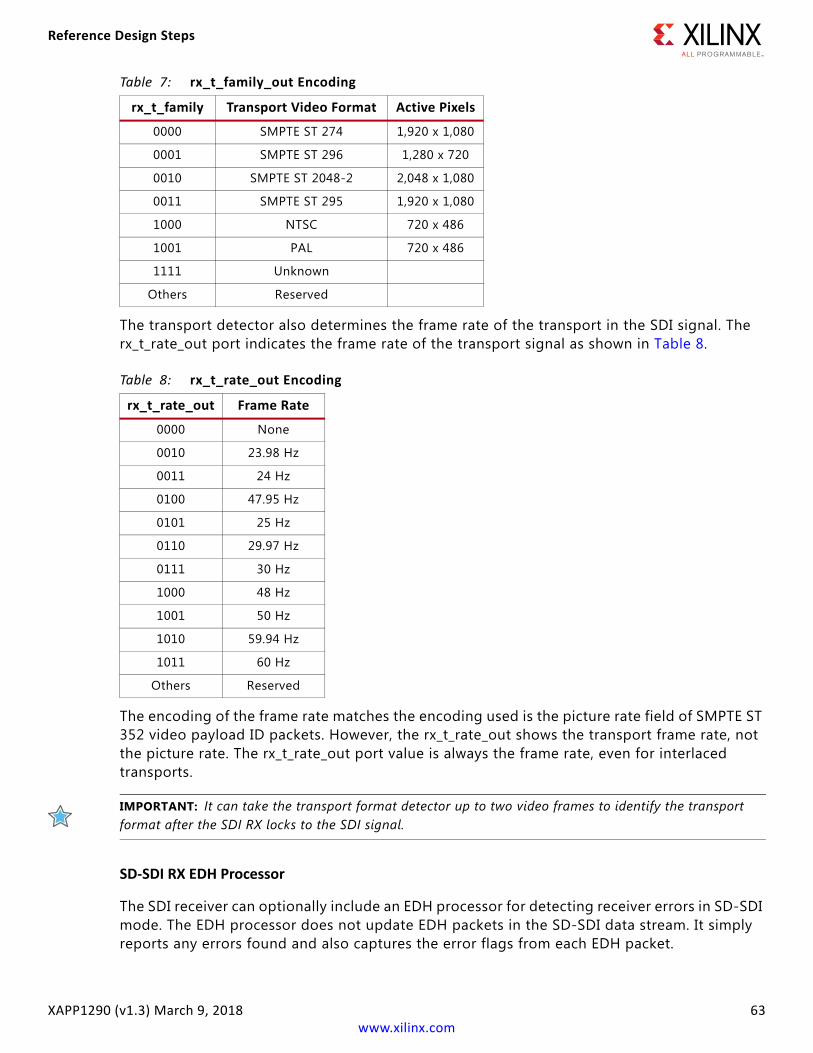
Reference Design Steps
XAPP1290 (v1.3) March 9, 2018 63www.xilinx.com
The transport detector also determines the frame rate of the transport in the SDI signal. The rx_t_rate_out port indicates the frame rate of the transport signal as shown in Table 8.
The encoding of the frame rate matches the encoding used is the picture rate field of SMPTE ST 352 video payload ID packets. However, the rx_t_rate_out shows the transport frame rate, not the picture rate. The rx_t_rate_out port value is always the frame rate, even for interlaced transports.
IMPORTANT: It can take the transport format detector up to two video frames to identify the transport format after the SDI RX locks to the SDI signal.
SD-SDI RX EDH Processor
The SDI receiver can optionally include an EDH processor for detecting receiver errors in SD-SDI mode. The EDH processor does not update EDH packets in the SD-SDI data stream. It simply reports any errors found and also captures the error flags from each EDH packet.
Table 7: rx_t_family_out Encoding
rx_t_family Transport Video Format Active Pixels
0000 SMPTE ST 274 1,920 x 1,080
0001 SMPTE ST 296 1,280 x 720
0010 SMPTE ST 2048-2 2,048 x 1,080
0011 SMPTE ST 295 1,920 x 1,080
1000 NTSC 720 x 486
1001 PAL 720 x 486
1111 Unknown
Others Reserved
Table 8: rx_t_rate_out Encoding
rx_t_rate_out Frame Rate
0000 None
0010 23.98 Hz
0011 24 Hz
0100 47.95 Hz
0101 25 Hz
0110 29.97 Hz
0111 30 Hz
1000 48 Hz
1001 50 Hz
1010 59.94 Hz
1011 60 Hz
Others Reserved
Reference Design Steps
XAPP1290 (v1.3) March 9, 2018 64www.xilinx.com
The EDH processor has a 16-bit counter that counts the number of fields with errors. The current error count is output on the rx_edh_errcnt_out port of the SDI wrapper. The counter is cleared by asserted rx_edh_clr_errcnt_in logic High. The user can specify which types of errors are counted by this counter using the rx_edh_errcnt_en_in port. This port has 16 unary bits that enable and disable 16 different error types. Any bit that is logic High enables the corresponding error to be counted by the error counter. Any bit that is logic Low disables the corresponding error. If multiple errors occur in the same field, the EDH error counter only increments by one. Table 9 shows the encoding of the bits on the rx_edh_errcnt_en_in port.
The ANC error conditions are associated with errors in the ancillary data packets. The FF error conditions are associated with errors detected by the full field CRC. The AP error conditions are associated with errors detected by the active picture CRC. The EDH packet checksum error indicates a checksum error was found within the EDH packet itself.
Each ANC, FF, and AP error condition set has five individual error flags. All flags are asserted logic High to indicate an error condition. For a complete description of the EDH, EDA, IDH, IDA, and UES error flags in the EDH packet, refer to the SMPTE RP 165 [Ref 1] document.
• EDH error: This error condition occurs when the EDH processor detects a CRC error (checksum error for ANC packets) in a field. For example, the FF EDH error flag indicates an error was detected by the full field CRC.
• EDA error: This error condition occurs when the EDA or EDH flags of the received EDH packet are asserted.
• IDH error: This error condition is not supported by the RX EDH processor.
Table 9: rx_edh_errcnt_en_in Bits
Bit Error
0 ANC EDH error
1 ANC EDA error
2 ANC IDH error
3 ANC IDA error
4 ANC UES error
5 FF EDH error
6 FF EDA error
7 FF IDH error
8 FF IDA error
9 FF UES error
10 AP EDH error
11 AP EDA error
12 AP IDH error
13 AP IDA error
14 AP UES error
15 EDH packet checksum error
Reference Design Steps
XAPP1290 (v1.3) March 9, 2018 65www.xilinx.com
• IDA error: This error condition occurs when the IDA or IDH flags of the received EDH packet are asserted.
• UES error: This error condition occurs when the UES flag in the received EDH packet is asserted.
In addition to being counted by the error counter, if it is enabled, any detected ANC EDH, AP EDH, and FF EDH errors are also indicated by assertion of the rx_edh_anc_out, rx_edh_ap_out, and rx_edh_ff_out ports, respectively. Thus, the rx_edh_anc port is asserted whenever a checksum error is detected in an ancillary data packet. The rx_edh_ap port is asserted when the calculated active picture CRC does not match the AP CRC in the EDH packet. The rx_edh_ff_out port is asserted when the calculated full field CRC does not match the FF CRC in the EDH packet.
The RX EDH processor also outputs the ANC, AP, and FF error flags from the EDH packet on the rx_edh_anc_flags_out, rx_edh_ap_flags_out, and rx_edh_ff_flags_out ports, respectively. These output ports are exact copies of the flags found in the last received EDH packet. Thus, they differ from the detected errors used to increment the error counter and output on the rx_edh_anc_out, rx_edh_ap_out, and rx_edh_ff_out ports. For example, the EDH flag (bit 0) of the rx_edh_ap_flags_out port indicates that the AP EDH flag was set in the last received EDH packet. However, the rx_edh_ap_out port indicates that the active picture CRC calculated locally by the EDH processor does not match the AP CRC value in the EDH packet.
The rx_edh_anc_flags_out, rx_edh_ap_flags_out, and rx_edh_ff_flags_out ports are each five bits wide. The encoding is identical for all three ports and is shown in Table 10.
The RX EDH processor also produces four error flags related to the format and contents of the EDH packet itself. These error flags are output on the rx_edh_packet_flags_out port. The encoding of this port is shown in Table 11.
GTH Initialization and Reset and Change Sequence Failure Codes
If a failure occurs during a GTH RX initialization or reset sequence or during a dynamic change of the RX SDI mode, the rx_change_fail_out port will be asserted logic High and a failure code
Table 10: Port Encoding of ANC, AP, and FF error flags
Bit Error
0 EDH
1 EDA
2 IDH
3 IDA
4 UES
Table 11: Encoding of rx_edh_packet_flags Port
Bit Error
0 EDH packet is missing
1 Parity error in user data words of EDH packet
2 Checksum error in EDH packet
3 Format error in EDH packet - such as invalid data count
Reference Design Steps
XAPP1290 (v1.3) March 9, 2018 66www.xilinx.com
will be output on the rx_change_fail_code_out port. A sequence only ends in failure once it has been retried the maximum number of times allowed by the retry counter. The maximum number of retries is controlled by the width of the retry counter as specified by the RX_RETRY_CNTR_MSB parameter or generic of the kugth_3gsdi_control.v in the SDI wrapper module. The number of retries attempted is:
Retries = 2 RX_RETRY_CNTR_MSB - 1
The encoding of the rx_change_fail_out port is shown in Table 12.
Any sequence failure that results in the rx_change_fail_out port going logic High will cause the GTH RX control logic in the SDI wrapper to stop in a failure condition. The GTH RX may still receive an SDI signal, but will not dynamically switch between SDI modes as it normally would. If a failure occurs as indicated by rx_change_fail_out going logic High, a GTH RX full reset must be done using the rx_rst_in and gth_wiz_reset_rx_pll_and_datapath_in. This output is synchronous with the gth_drpclk_in. Repeated failures most likely indicate a problem with the design of the application.
If a failure occurs during a GTH TX initialization or reset sequence or during a dynamic change of the TX SDI mode, the tx_change_fail_out port will be asserted logic High and a failure code
Table 12: rx_change_fail_code_out Port Encoding
Code Description
0 Reserved
1
When a change of the RX SDI mode is requested that requires changing the RXCDR_CFG2 attribute in the GTH transceiver, the kugth_3gsdi_control module attempts to do a DRP write cycle to change that attribute. If thekugth_3gsdi_drp_control module detected a mismatch between the written RXCDR_CFG2 value and its actual content after retries, the sequence fails with this failure code.
2
When a change of the RX SDI mode is requested that requires changing the RXOUT_DIV attribute in the GTH transceiver, the kugth_3gsdi_drp_control module attempts to do a DRP write cycle to change that attribute. If the kugth_3gsdi_drp_control module detected a mismatch between the written RXOUT_DIV value and its actual content after retries, the sequence fails with this failure code.
3
The gtwiz_reset_rx_datapath_in port of the GTH Wizard IP is asserted after completing a series for DRP and GTH port during a dynamic change to reset the GTH RX portion. If the gtwiz_reset_rx_done_out port of GTH Wizard IP failed to assert after retries, the sequence fails with this failure code.
4
When a change of the RX SDI mode is requested that requires changing the RXDATA_WIDTH attribute in the GTH transceiver, the kugth_3gsdi_control module attempts to do a DRP write cycle to change that attribute. If the kugth_3gsdi_drp_control module detected a mismatch between the written RXDATA_WIDTH value and its actual content after retries, the sequence fails with this failure code.
5
When a change of the RX SDI mode is requested that requires changing the RXINT_DATAWIDTH attribute in the GTH transceiver, the kugth_3gsdi_control module attempts to do a DRP write cycle to change that attribute. If the kugth_3gsdi_drp_control module detected a mismatch between the written RXINT_DATAWIDTH value and its actual content after retries, the sequence fails with this failure code.
6 Reserved.
7 Reserved.
Reference Design Steps
XAPP1290 (v1.3) March 9, 2018 67www.xilinx.com
will be output on the tx_change_fail_code_out port. A sequence only ends in failure once it has been retried the maximum number of times allowed by the retry counter. The maximum number of retries is controlled by the width of the retry counter as specified by the TX_RETRY_CNTR_MSB parameter or generic of the kugth_3gsdi_control.v in the SDI wrapper module.
The number of retries attempted is:
Retries = 2 TX_RETRY_CNTR_MSB - 1
The encoding of the tx_change_fail_code port is shown in Table 13.
Apply Timing Constraints
For the SDI wrapper and the SDI core, only the periods of the clocks listed here must be constrained:
• Clock applied to the clk port in the SDI wrapper
• Clock applied to the drpclk port in the SDI wrapper
• tx_outclk signal in the SDI wrapper
• rx_outclk signal in the SDI wrapper
Table 13: tx_change_fail_code_out Port Encoding
Code Description
0 Reserved
1 When a change of the TX SDI mode is requested that requires changing the TXDATA_WIDTH attribute in the GTH transceiver, the kugth_3gsdi_control module attempts to do a DRP write cycle to change that attribute. If the kugth_3gsdi_drp_control module detected a mismatch between the written TXDATA_WIDTH value and its actual content after retries, the sequence fails with this failure code.
2 When a change of the TX SDI mode is requested that requires changing the TXINT_DATAWIDTH attribute in the GTH transceiver, the kugth_3gsdi_control module attempts to do a DRP write cycle to change that attribute. If the vkugth_3gsdi_drp_control module detected a mismatch between the written TXINT_DATAWIDTH value and its actual content after retries, the sequence fails with this failure code.
3 When a change of the TX SDI mode is requested that requires changing the TXOUT_DIV attribute in the GTH transceiver, the kugth_3gsdi_control module attempts to do a DRP write cycle to change that attribute. If the kugth_3gsdi_drp_control module detected a mismatch between the written TXOUT_DIV value and its actual content after retries, the sequence fails with this failure code.
4 The gtwiz_reset_tx_datapath_in port of the GTH Wizard IP is asserted after completing a series for DRP and GTH port during a dynamic change to reset the GTH TX portion. If the gtwiz_reset_tx_done_out port of GTH Wizard IP failed to assert after retries, the sequence fails with this failure code.
5 Reserved.
6 Reserved.
7 Reserved.
Reference Design Steps
XAPP1290 (v1.3) March 9, 2018 68www.xilinx.com
The tx_outclk and rx_outclk clocks are usually constrained to 148.5 MHz, sometimes rounded up to 150 MHz.
Vivado tools consider all clocks to be related, unless told otherwise. The various clocks of the SDI wrapper are generally unrelated, so a constraint is required to specify that these clocks are not related.
See the timing constraints files of the example SDI demonstration provided with the example SDI design for examples.
Compiling the SDI Demonstration
Compiling the reference design is done in four steps and takes about 30 minutes to finish. Follow the instructions below to begin the compilation.
1. Unzip xapp1290-smpte-3gsdi-with-kintex-us-gth-trans.zip.
2. Open Vivado Design Suite 2018.1 or later
3. In the Vivado Tcl Console, Enter:
4. cd <unzip_dir>\xapp1290.
5. source all.tcl
6. Wait for project compilation to finish
The Tcl script executes 6 steps to complete the bitstream generation.
1. Creating Project
2. Importing RTL sources
3. Adding design constraint files
4. Generating Xilinx IPs:
° tx_vio
° rx_vio
° rx_ila
5. GT Wizard IP for x0y16 (v_smpte_sdi_gtwiz_x0y16)
6. Build IPI Subsystem for inrevium 12G-SDI FMC Card control
7. Running compilation
IMPORTANT: ES devices requires special prohibit constraint to prevent Vivado from routing design with defective LUT RAMs. Talk to your FAE for more details.
Recompile the FMC controller SDK Project
After the completing the all.tcl script, prepare The SDK environment by exporting the project hardware information and importing the SDK source codes:
Reference Design Steps
XAPP1290 (v1.3) March 9, 2018 69www.xilinx.com
1. In Vivado Design Suite select, File > Export > Export Hardware.
2. In the Export Hardware window:
a. Select Include bitstream option.
b. Set the Export to: <unzip_dir>\xapp1290\srcs\fidus_fmc_ctlr\SW.
3. Select File > Launch SDK to launch the SDK integrated design environment (IDE).
a. In the exported location and workspace fields, enter <unzip_dir>\xapp1290\srcs\fidus_fmc_ctlr\SW.
b. Select File > New > Board Support Package in the board support package window.
c. Enter fidus_fmc_ctlr_bsp in the project name field, and click Finish.
d. In the board support package settings, click OK.
4. In the SDK IDE, select, File > Import.
5. In the Import pop-up window:
a. Select General. > Existing Projects.
b. Click Next.
c. Click Browse… and verify that it points to the corresponding folders<unzip_dir>\xapp1290\srcs\fidus_fmc_ctlr\SW.
d. Click OK.
e. Make sure fidus_fmc_ctlr is checked
f. Click Finish.
6. Assign fidus_fmc_ctlr_bsp to fidus_fmc_ctlr:
a. In SDK, right click fidus_fmc_ctlr folder.
b. Click Change Referenced BSP.
c. Select fidus_fmc_ctlr_bsp and click OK.
Results
This document describes how to use the SMPTE SD/HD/3G-SDI LogiCORE IP core and the GTH transceivers available in Kintex UltraScale FPGAs to implement SDI interfaces compatible with the SMPTE SD-SDI, HD-SDI and 3G-SDI standards. The device-specific control logic necessary to implement GTH transceivers in SDI applications is included with the example SDI design that accompanies this application note. Also included are two example SDI demonstration applications providing detailed examples of SDI implementations for use in a Kintex UltraScale FPGA design.
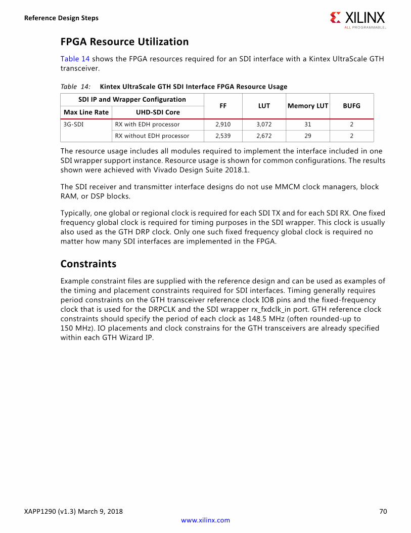
Reference Design Steps
XAPP1290 (v1.3) March 9, 2018 70www.xilinx.com
FPGA Resource Utilization
Table 14 shows the FPGA resources required for an SDI interface with a Kintex UltraScale GTH transceiver.
The resource usage includes all modules required to implement the interface included in one SDI wrapper support instance. Resource usage is shown for common configurations. The results shown were achieved with Vivado Design Suite 2018.1.
The SDI receiver and transmitter interface designs do not use MMCM clock managers, block RAM, or DSP blocks.
Typically, one global or regional clock is required for each SDI TX and for each SDI RX. One fixed frequency global clock is required for timing purposes in the SDI wrapper. This clock is usually also used as the GTH DRP clock. Only one such fixed frequency global clock is required no matter how many SDI interfaces are implemented in the FPGA.
Constraints
Example constraint files are supplied with the reference design and can be used as examples of the timing and placement constraints required for SDI interfaces. Timing generally requires period constraints on the GTH transceiver reference clock IOB pins and the fixed-frequency clock that is used for the DRPCLK and the SDI wrapper rx_fxdclk_in port. GTH reference clock constraints should specify the period of each clock as 148.5 MHz (often rounded-up to 150 MHz). IO placements and clock constrains for the GTH transceivers are already specified within each GTH Wizard IP.
Table 14: Kintex UltraScale GTH SDI Interface FPGA Resource Usage
SDI IP and Wrapper ConfigurationFF LUT Memory LUT BUFG
Max Line Rate UHD-SDI Core
3G-SDI RX with EDH processor 2,910 3,072 31 2
RX without EDH processor 2,539 2,672 29 2
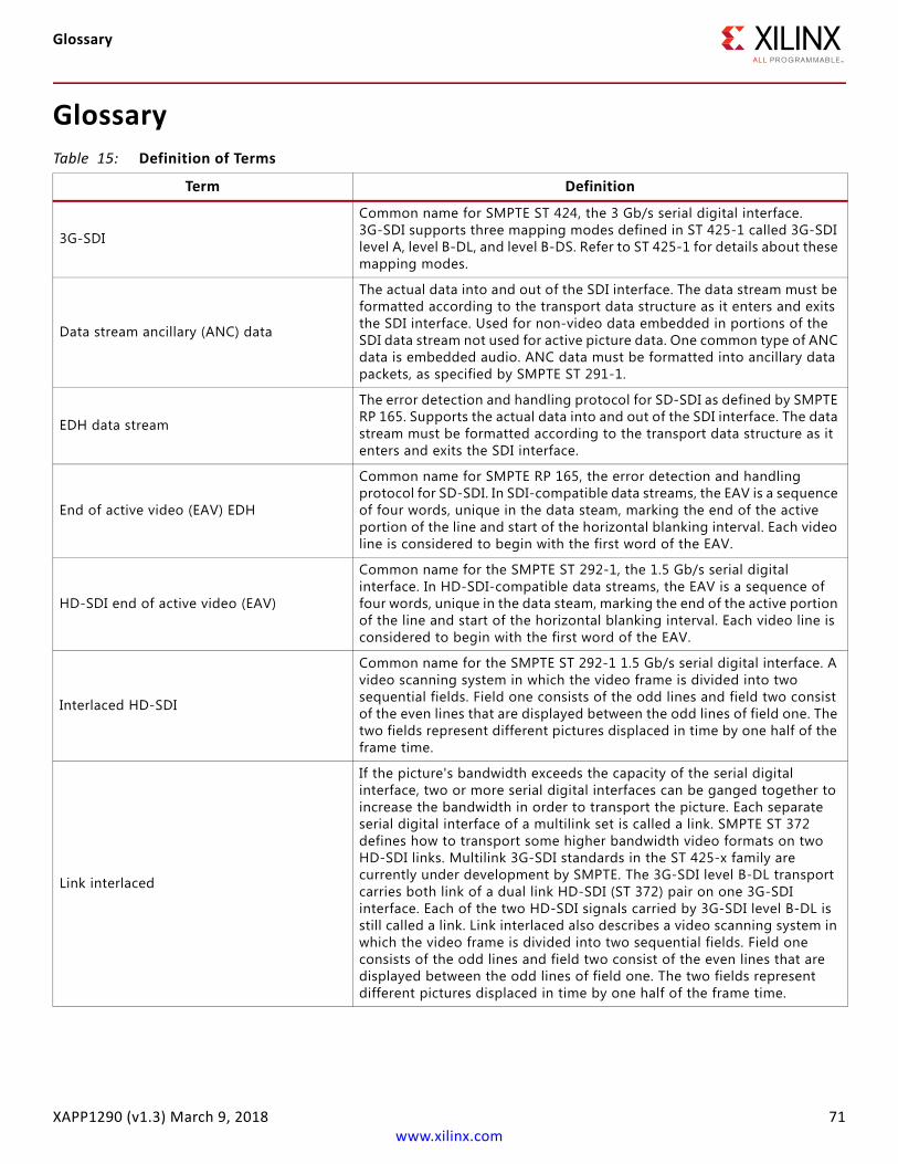
Glossary
XAPP1290 (v1.3) March 9, 2018 71www.xilinx.com
Glossary
Table 15: Definition of Terms
Term Definition
3G-SDI
Common name for SMPTE ST 424, the 3 Gb/s serial digital interface. 3G-SDI supports three mapping modes defined in ST 425-1 called 3G-SDI level A, level B-DL, and level B-DS. Refer to ST 425-1 for details about these mapping modes.
Data stream ancillary (ANC) data
The actual data into and out of the SDI interface. The data stream must be formatted according to the transport data structure as it enters and exits the SDI interface. Used for non-video data embedded in portions of the SDI data stream not used for active picture data. One common type of ANC data is embedded audio. ANC data must be formatted into ancillary data packets, as specified by SMPTE ST 291-1.
EDH data stream
The error detection and handling protocol for SD-SDI as defined by SMPTE RP 165. Supports the actual data into and out of the SDI interface. The data stream must be formatted according to the transport data structure as it enters and exits the SDI interface.
End of active video (EAV) EDH
Common name for SMPTE RP 165, the error detection and handling protocol for SD-SDI. In SDI-compatible data streams, the EAV is a sequence of four words, unique in the data steam, marking the end of the active portion of the line and start of the horizontal blanking interval. Each video line is considered to begin with the first word of the EAV.
HD-SDI end of active video (EAV)
Common name for the SMPTE ST 292-1, the 1.5 Gb/s serial digital interface. In HD-SDI-compatible data streams, the EAV is a sequence of four words, unique in the data steam, marking the end of the active portion of the line and start of the horizontal blanking interval. Each video line is considered to begin with the first word of the EAV.
Interlaced HD-SDI
Common name for the SMPTE ST 292-1 1.5 Gb/s serial digital interface. A video scanning system in which the video frame is divided into two sequential fields. Field one consists of the odd lines and field two consist of the even lines that are displayed between the odd lines of field one. The two fields represent different pictures displaced in time by one half of the frame time.
Link interlaced
If the picture's bandwidth exceeds the capacity of the serial digital interface, two or more serial digital interfaces can be ganged together to increase the bandwidth in order to transport the picture. Each separate serial digital interface of a multilink set is called a link. SMPTE ST 372 defines how to transport some higher bandwidth video formats on two HD-SDI links. Multilink 3G-SDI standards in the ST 425-x family are currently under development by SMPTE. The 3G-SDI level B-DL transport carries both link of a dual link HD-SDI (ST 372) pair on one 3G-SDI interface. Each of the two HD-SDI signals carried by 3G-SDI level B-DL is still called a link. Link interlaced also describes a video scanning system in which the video frame is divided into two sequential fields. Field one consists of the odd lines and field two consist of the even lines that are displayed between the odd lines of field one. The two fields represent different pictures displaced in time by one half of the frame time.
Glossary
XAPP1290 (v1.3) March 9, 2018 72www.xilinx.com
Payload ID link
Sometimes called the Video Payload ID (VPID), the payload ID is an ancillary data packet defined by SMPTE Payload Identifier Codes for Serial Digital Interfaces (ST 352) [Ref 1]. The four data words of the ST 352 payload ID packet identify both the nature of the video picture (video format, frame rate, scanning structure, color space, and so on) and the type of SDI interface used to transport that payload. In multilink interfaces, the payload ID also contains bits that distinguish between the individual links.
Progressive payload ID
A non-interlaced video scanning system. All lines of the progressive frame belong to the same picture. Sometimes called the Video Payload ID (VPID), the payload ID is an ancillary data packet defined by SMPTE ST 352. The four data words of the ST 352 payload ID packet identify both the nature of the video picture (video format, frame rate, scanning structure, color space, etc) and the type of SDI interface used to transport that payload. In multilink interfaces, the payload ID also contains bits that distinguish between the individual links.
Serial Digital interface (SDI) progressive
Originally referred to as SMPTE ST 259, the standard-definition serial digital interface. With the advent of HD-SDI and 3G-SDI, ST 259 is now often called SD-SDI to avoid confusion. This document uses the term SDI to generically refer to SD-SDI, HD-SDI and 3G-SDI. When referring specifically to ST 259, this document always uses the term SD-SDI. A non-interlaced video scanning system. All lines of the progressive frame belong to the same picture.
SD-SDI serial digital interface (SDI)
Common name for SMTPE ST 259, the standard-definition serial digital interface. Originally referred to SMPTE ST 259, the standard-definition serial digital interface. With the advent of HD-SDI and 3G-SDI, ST 259 is now often called SD-SDI to avoid confusion. This document uses the term SDI to generically refer to SD-SDI, HD-SDI and 3G-SDI. When referring specifically to ST 259, this document always uses the term SD-SDI.
SMPTE SD-SDI Society of Motion Picture and Television Engineers common name for SMTPE ST 259, the standard-definition serial digital interface.
Start of active video (SAV) SMPTE
In SDI compatible data streams, the SAV is a sequence of four words, unique in the data stream, marking the end of the horizontal blanking interval and the start of the active video portion of the line. The first active video sample of a line, usually called sample 0, occurs immediately after the SAV.
Synchronous switching (point, interval, line)start of active video (SAV)
SMPTE RP 168 defines the point(s) in a video frame where it is permissible to switch between synchronous video sources. This is often called the synchronous switching point, but is actually defined as an interval, which is a portion of a line, rather than an exact point on a line. The line that contains the synchronous switching interval is sometimes called the synchronous switching line. In SDI-compatible data streams, the SAV is a sequence of four words, unique in the data stream, marking the end of the horizontal blanking interval and the start of the active video portion of the line. The first active video sample of a line, usually called sample 0, occurs immediately after the SAV.
Table 15: Definition of Terms (Cont’d)
Term Definition
Documentation Navigator and Design Hubs
XAPP1290 (v1.3) March 9, 2018 73www.xilinx.com
Documentation Navigator and Design HubsXilinx Documentation Navigator provides access to Xilinx documents, videos, and support resources, which you can filter and search to find information. To open the Xilinx Documentation Navigator (DocNav):
• From the Vivado IDE, select Help > Documentation and Tutorials.
• On Windows, select Start > All Programs > Xilinx Design Tools > DocNav.
• At the Linux command prompt, enter docnav.
Xilinx Design Hubs provide links to documentation organized by design tasks and other topics, which you can use to learn key concepts and address frequently asked questions. To access the Design Hubs:
• In the Xilinx Documentation Navigator, click the Design Hubs View tab.
• On the Xilinx website, see the Design Hubs page.
Note: For more information on Documentation Navigator, see the Documentation Navigator page on the Xilinx website.
Transport synchronous switching(point, interval, line)
The data structure of an interface data stream or streams. The transport data structure defines the EAV and SAV sequences used to carry video timing information. SMPTE RP 168 defines the point(s) in a video frame where it is permissible to switch between synchronous video sources. This is often called the synchronous switching point, but is actually defined as an interval, which is a portion of a line, rather than an exact point on a line. The line that contains the synchronous switching interval is sometimes called the synchronous switching line.
Timing reference signal (TRS) transport
A generic term referring to both EAV and SAV sequences. The data structure of an interface data stream or streams. The transport data structure defines the EAV and SAV sequences used to carry video timing information.
XYZ timing reference signal (TRS)
The fourth word of each EAV and SAV is called the XYZ word. This word carries the horizontal (H), vertical (V), and field (F) bits that indicate the video timing. The XYZ word also contains protection bits that allow detection of errors in the XYZ word. It is also used as a generic term referring to both EAV and SAV sequences.
XYZ
The fourth word of each EAV and SAV is called the XYZ word. This word carries the horizontal (H), vertical (V), and field (F) bits that indicate the video timing. The XYZ word also contains protection bits that allow detection of errors in the XYZ word.
Table 15: Definition of Terms (Cont’d)
Term Definition
References
XAPP1290 (v1.3) March 9, 2018 74www.xilinx.com
References1. Available from the Society of Motion Picture and Television Engineers (www.smpte.org):
Error Detection Checkwords and Status Flags for Use in Bit-Serial Digital Interfaces for Television (RP 165)
Definition of Vertical Switching Point for Synchronous Video Switching (RP 168)
Television - SDTV Digital Signal/Data - Serial Digital Interface (ST 259)
Television - Ancillary Data Packet and Space Formatting (ST 291-1)
1.5 Gb/s Signal/Data Serial Interface (ST 292-1)
Television - 540 Mb/s Serial Digital Interface (ST 344)
Payload Identifier Codes for Serial Digital Interfaces (ST 352)
Dual Link 1.5 Gb/s Digital Interface for 1920 x 1080 and 2048 x 1080 Picture Formats (ST 372)
Television - 3 Gb/s Signal/Data Serial Interface (ST 424)
Source Image Format and Ancillary Data Mapping for the 3Gb/s Serial Interface (ST 425-1)
2. Kintex UltraScale FPGAs Data Sheet: DC and AC Switching Characteristics (DS892)
3. SMPTE SD/HD/3G-SDI 3.0 LogiCORE IP Product Guide (PG071)
4. UltraScale FPGAs Transceivers Wizard LogiCORE IP Product Guide (PG182)
5. UltraScale Architecture GTH Transceivers User Guide (UG576)
6. 7 Series FPGAs GTP Transceivers User Guide (UG482)
7. Dynamically Programmable DRU for High-Speed Serial I/O (XAPP875)
8. KCU105 Evaluation Kit (www.xilinx.com/kcu105)
9. KCU105 Board User Guide (UG917)
10. Fidus inrevium 6G/12G SDI FPGA Mezzanine Card
° Xilinx webpage www.xilinx.com/products/boards-and-kits/1-5ky5ij.html)
° Fidus Systems webpage: www.fidus.com
11. Tera Term Terminal Emulator Installation Guide (UG1036)
12. Silicon Labs CP210x USB-to-UART Installation Guide (UG1033)
13. Vivado Design Suite Tutorial Programming and Debugging (UG936)
14. E.G PHABRIX SxE Eye and Jitter video test generator monitor and analyzer (www.phabrix.com)
Revision History
XAPP1290 (v1.3) March 9, 2018 75www.xilinx.com
Revision HistoryThe following table shows the revision history for this document.
Please Read: Important Legal NoticesThe information disclosed to you hereunder (the “Materials”) is provided solely for the selection and use of Xilinx products. To the maximum extent permitted by applicable law: (1) Materials are made available “AS IS” and with all faults, Xilinx hereby DISCLAIMS ALL WARRANTIES AND CONDITIONS, EXPRESS, IMPLIED, OR STATUTORY, INCLUDING BUT NOT LIMITED TO WARRANTIES OF MERCHANTABILITY, NON-INFRINGEMENT, OR FITNESS FOR ANY PARTICULAR PURPOSE; and (2) Xilinx shall not be liable (whether in contract or tort, including negligence, or under any other theory of liability) for any loss or damage of any kind or nature related to, arising under, or in connection with, the Materials (including your use of the Materials), including for any direct, indirect, special, incidental, or consequential loss or damage (including loss of data, profits, goodwill, or any type of loss or damage suffered as a result of any action brought by a third party) even if such damage or loss was reasonably foreseeable or Xilinx had been advised of the possibility of the same. Xilinx assumes no obligation to correct any errors contained in the Materials or to notify you of updates to the Materials or to product specifications. You may not reproduce, modify, distribute, or publicly display the Materials without prior written consent. Certain products are subject to the terms and conditions of Xilinx’s limited warranty, please refer to Xilinx’s Terms of Sale which can be viewed at https://www.xilinx.com/legal.htm#tos; IP cores may be subject to warranty and support terms contained in a license issued to you by Xilinx. Xilinx products are not designed or intended to be fail-safe or for use in any application requiring fail-safe performance; you assume sole risk and liability for use of Xilinx products in such critical applications, please refer to Xilinx’s Terms of Sale which can be viewed at https://www.xilinx.com/legal.htm#tos.AUTOMOTIVE APPLICATIONS DISCLAIMERAUTOMOTIVE PRODUCTS (IDENTIFIED AS "XA" IN THE PART NUMBER) ARE NOT WARRANTED FOR USE IN THE DEPLOYMENT OF AIRBAGS OR FOR USE IN APPLICATIONS THAT AFFECT CONTROL OF A VEHICLE ("SAFETY APPLICATION") UNLESS THERE IS A SAFETY CONCEPT OR REDUNDANCY FEATURE CONSISTENT WITH THE ISO 26262 AUTOMOTIVE SAFETY STANDARD ("SAFETY DESIGN"). CUSTOMER SHALL, PRIOR TO USING OR DISTRIBUTING ANY SYSTEMS THAT INCORPORATE PRODUCTS, THOROUGHLY TEST SUCH SYSTEMS FOR SAFETY PURPOSES. USE OF PRODUCTS IN A SAFETY APPLICATION WITHOUT A SAFETY DESIGN IS FULLY AT THE RISK OF CUSTOMER, SUBJECT ONLY TO APPLICABLE LAWS AND REGULATIONS GOVERNING LIMITATIONS ON PRODUCT LIABILITY.© Copyright 2016–2018 Xilinx, Inc. Xilinx, the Xilinx logo, Artix, ISE, Kintex, Spartan, Virtex, Vivado, Zynq, and other designated brands included herein are trademarks of Xilinx in the United States and other countries. All other trademarks are the property of their respective owners.
Date Version Changes
03/09/2018 1.3 Updated for Vivado 2018.1.
10/02/2017 1.2 Updated descriptions for tx_ce_in, tx_sd_ce_in, and tx_edh_ce_in in SDI Wrapper Port List table.
09/29/2016 1.1 Updated to core version 1.1.
06/24/2016 1.0 Initial Xilinx release.