Embed Size (px)
DESCRIPTION
Implementing High-speed String Matching Hardware for Network Intrusion Detection Systems. Author: Atul Mahajan, Benfano Soewito, Sai K. Parsi, Ning Weng and Haibo Wang Publisher: Proceedings of the 16th international ACM/SIGDA symposium on Field programmable gate arrays, FPGA 2008 Presenter: - PowerPoint PPT Presentation
Citation preview
Author:Atul Mahajan, Benfano Soewito, Sai K. Parsi, Ning Weng and Haibo Wang
Publisher:Proceedings of the 16th international ACM/SIGDA symposium on Field programmable gate arrays, FPGA 2008
Presenter: Chin-Chung Pan
Date: 2009/11/11
OutlineIntroductionTechniques for high-throughput verifier
DesignMulti-threading FSMHigh-speed interface circuit designMinimizing FSM interconnect delay
Experimental Results
2
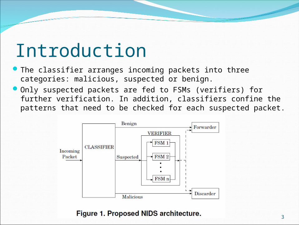
IntroductionThe classifier arranges incoming packets into three
categories: malicious, suspected or benign.Only suspected packets are fed to FSMs (verifiers) for further
verification. In addition, classifiers confine the patterns that need to be checked for each suspected packet.
3
OutlineIntroductionTechniques for high-throughput verifier
DesignMulti-threading FSMHigh-speed interface circuit designMinimizing FSM interconnect delay
Experimental Results
4
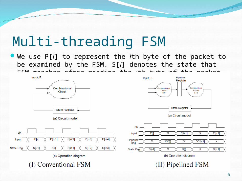
Multi-threading FSM
5
We use P[i] to represent the ith byte of the packet to be examined by the FSM. S[i] denotes the state that FSM reaches after reading the ith byte of the packet.
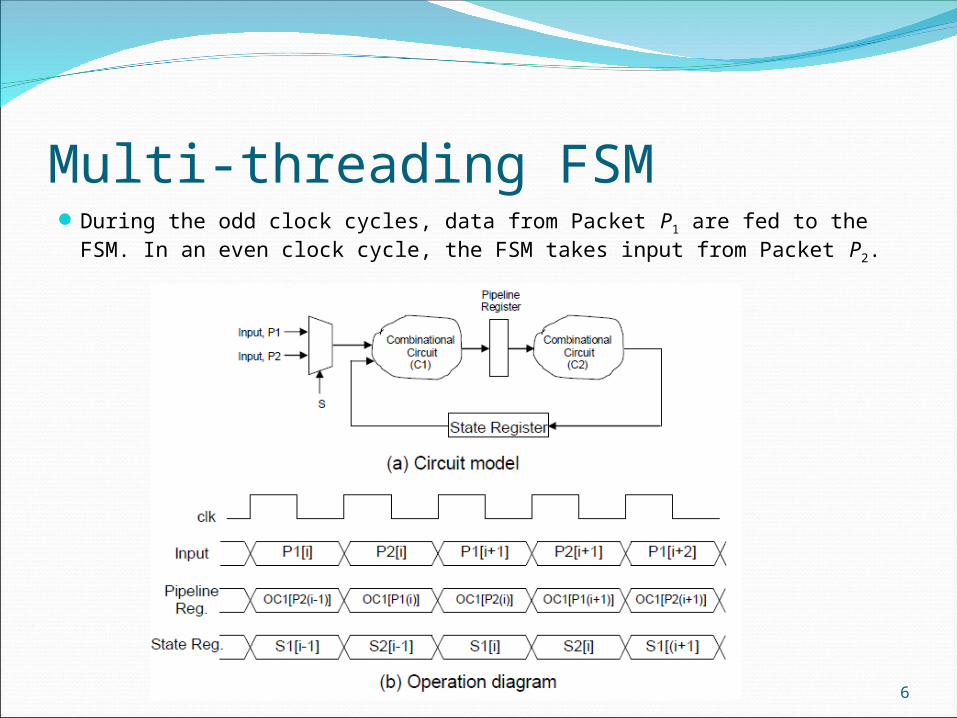
Multi-threading FSMDuring the odd clock cycles, data from Packet P1 are fed to the FSM. In an even
clock cycle, the FSM takes input from Packet P2.
6
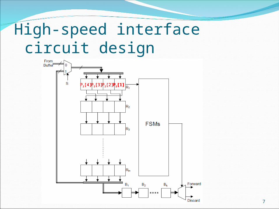
High-speed interface circuit design
7
P1[1]P1[2]P1[3]P1[4] P1[1]P2[2]P2[3]P2[4] P2[1]
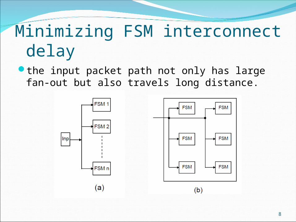
Minimizing FSM interconnect delay the input packet path not only has large fan-out but also
travels long distance.
8
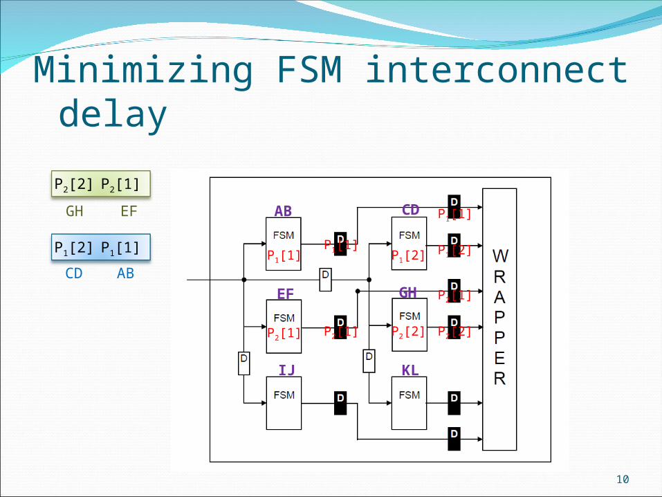
Minimizing FSM interconnect delay
10
P1[1] P1[2]P1[1]
P1[1]
P1[2]
P2[1] P2[2]P2[1]
P2[1]
P2[2]
P1[1]P1[2]
P2[1]P2[2]
ABCD
EFGH AB CD
EF GH
IJ KL
OutlineIntroductionTechniques for high-throughput verifier
DesignMulti-threading FSMHigh-speed interface circuit designMinimizing FSM interconnect delay
Experimental Results
11
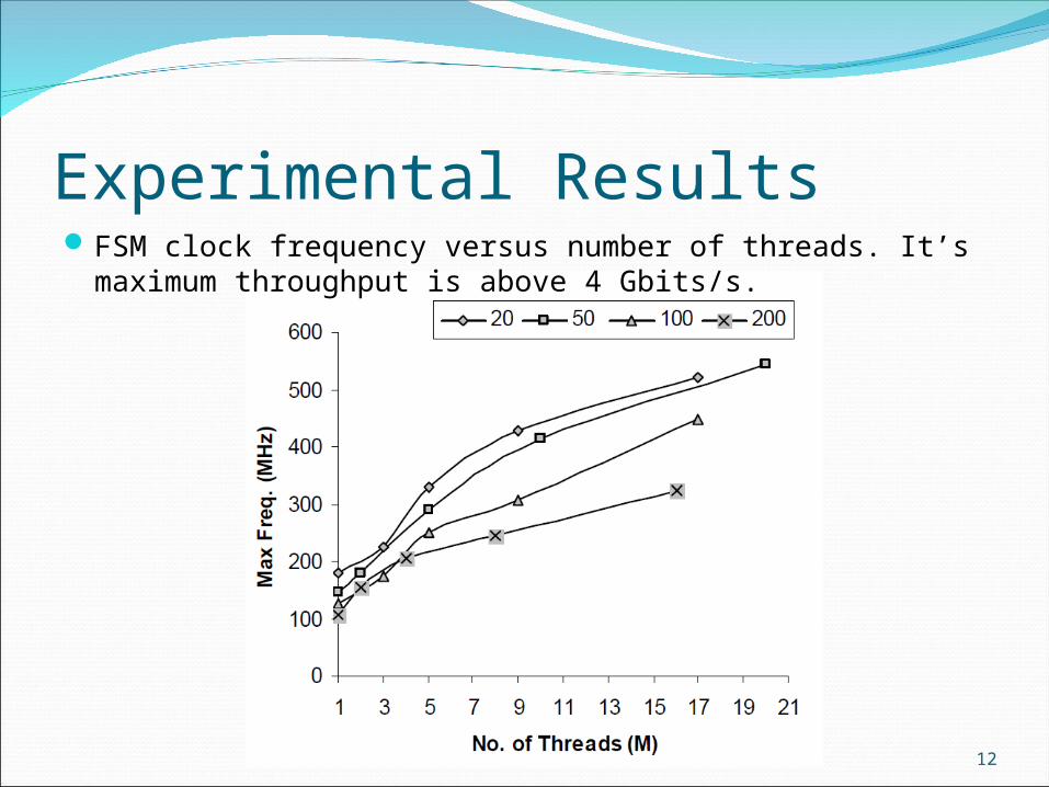
Experimental ResultsFSM clock frequency versus number of threads. It’s maximum throughput
is above 4 Gbits/s.
12
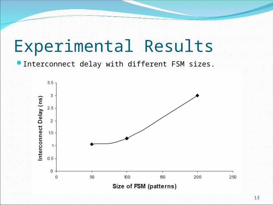
Experimental ResultsInterconnect delay with different FSM sizes.
13
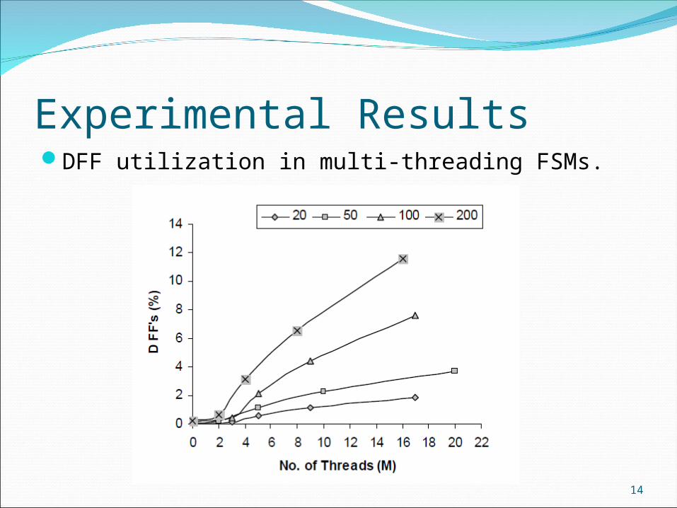
Experimental ResultsDFF utilization in multi-threading FSMs.
14
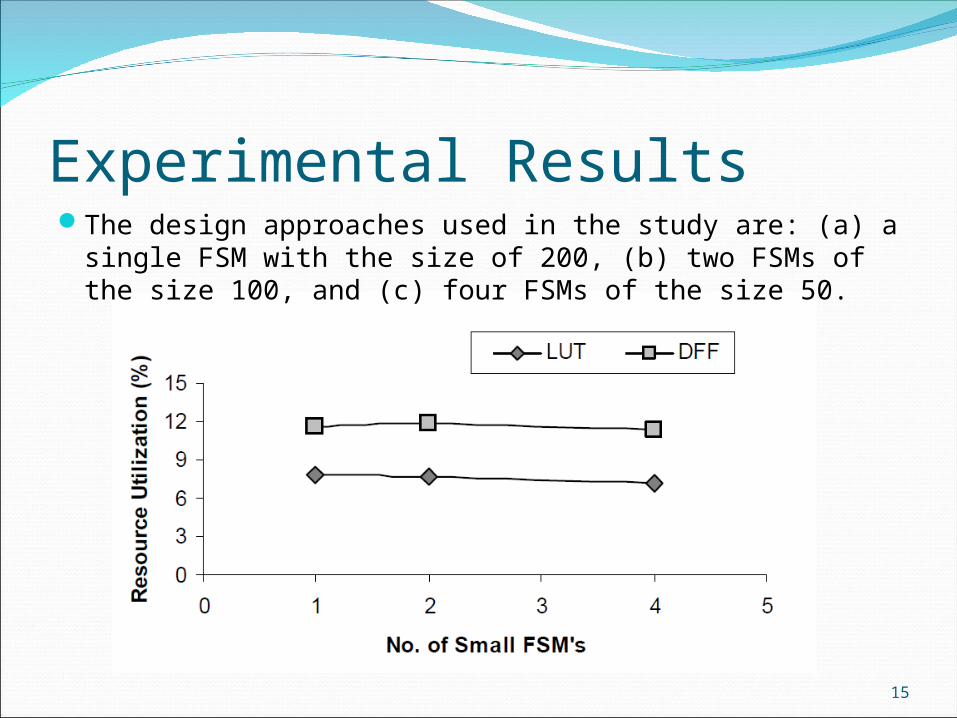
Experimental ResultsThe design approaches used in the study are: (a) a single FSM with
the size of 200, (b) two FSMs of the size 100, and (c) four FSMs of the size 50.
15
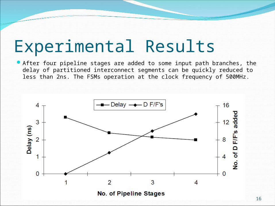
Experimental ResultsAfter four pipeline stages are added to some input path branches, the delay
of partitioned interconnect segments can be quickly reduced to less than 2ns. The FSMs operation at the clock frequency of 500MHz.
16