Embed Size (px)
Citation preview
Application Note
Implementing an 8b/10b Encoder/Decoder for Gigabit Ethernet in the Actel SX FPGA Family
IntroductionThis application note describes how an Actel A54SX16 FPGAwas used to implement an 8b/10b encoder/decoder functionfor a Gigabit Ethernet router.
The Gigabit Ethernet standards committee selected 8b/10btransmission coding for the physical coding sublayer. Thedefinition for the 8b/10b transmission code specified in theIEEE 802.3z specification is identical to that of the ANSIX3.230-1994 (Fibre Channel FC-PH) specification. The 8b/10btransmission code was developed by Albert X. Widmer andPeter A. Franaszek of IBM Corporation in the early ’80s. Anexcellent article on the development of this transmissioncode was published in the September 1983 IBM Researchand Development Journal (Vol. 27 No. 5). The articledescribes the logic gates required to implement the encodingand decoding functions explicitly.
The 8b/10b transmission code converts a byte wide datastream of random 1s and 0s into a DC balanced stream of 1sand 0s with a maximum run length of 5. The code must alsoprovide sufficient signal transitions to enable reliable clockrecovery. A DC balanced data stream proves to beadvantageous for fiber optic and electromagnetic wireconnections. The average number of 1s and 0s in the serialstream must be maintained at equal or near equal levels. The8b/10b transmission code constrains the disparity betweenthe number of 1s and 0s to be –2, 0, or 2 across 6 and 4 bitblock boundaries. Certain 10 bit codes in the 8b/10btransmission code have a nonzero disparity value of ±2. Thesecodes require the encoder circuitry to retain the state of thecurrent disparity and select the appropriate ±2 valueencoding pair for transmission to maintain DC balance. Thecoding scheme also implements additional codes forsignaling, called command codes.
Implementation Requirements
There are several pin-compatible 3.3V Gigabit Ethernettransceiver devices currently available on the market. Thesedevices provide for the serialization, clock recovery, bytesynchronization, and de-serialization of the Gigabit Ethernetdata stream. However, these devices do not perform the8b/10b encoding and decoding functions. The transmittersection of the transceiver requires a 125 MHz clock and a 10bit encoded data value with a setup time of 1.5 ns and a holdtime of 1.0 ns. Because of the 1.5 ns setup time, the Tco of the
encoder must be 5.5 ns, allowing a 1.0 ns provision for PCBtrace delay and device to device clock skew. The receiversection of the transceiver requires two orthogonal 62.5 MHzclocks and 10 bits of data with a Tco of 5.0 to 5.5 ns and a holdtime of 1.5 to 2.0 ns. The Tsu and Th for the decoder circuitmust be 1.5 ns and 0 ns respectively, again allowing a 1.0 nsprovision for PCB trace delay and device to device clock skew.
The Programmable Logic Challenge
There are several challenges in implementing an 8b/10bencoder/decoder (ENDEC) in a programmable logic device.The device must have sufficient 3.3V internal speed to meetthe 8 ns register to register requirement of the encoder, and3.3V I/O performance to meet the 5.0 ns Tco requirement.The low input setup requirements for the decoder wouldnormally require the use of specialized I/O cell registers, butthe dual clocking requirement resulting from the orthogonalclocks prevents this. The two 62.5 MHz orthogonal clocksallow the design to employ two identical decoder circuits, butthe overall decoder design must still check the runningdisparity between the two decoders for the incoming datastream. A single device solution must have a minimum ofthree high speed, low skew clock networks to meet the designperformance requirements. The Actel SX family satisfiesthese requirements.
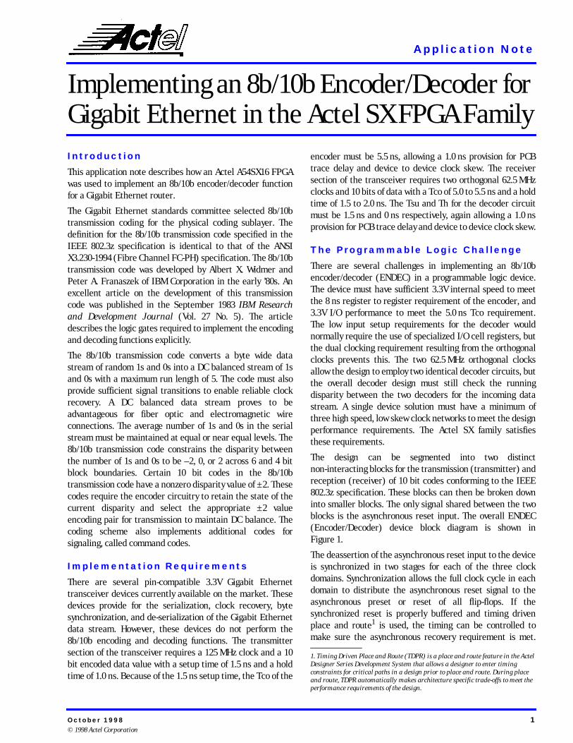
The design can be segmented into two distinctnon-interacting blocks for the transmission (transmitter) andreception (receiver) of 10 bit codes conforming to the IEEE802.3z specification. These blocks can then be broken downinto smaller blocks. The only signal shared between the twoblocks is the asynchronous reset input. The overall ENDEC(Encoder/Decoder) device block diagram is shown inFigure 1.
The deassertion of the asynchronous reset input to the deviceis synchronized in two stages for each of the three clockdomains. Synchronization allows the full clock cycle in eachdomain to distribute the asynchronous reset signal to theasynchronous preset or reset of all flip-flops. If thesynchronized reset is properly buffered and timing drivenplace and route1 is used, the timing can be controlled tomake sure the asynchronous recovery requirement is met.
1. Timing Driven Place and Route (TDPR) is a place and route feature in the Actel Designer Series Development System that allows a designer to enter timing constraints for critical paths in a design prior to place and route. During place and route, TDPR automatically makes architecture specific trade-offs to meet the performance requirements of the design.
October 1998 1© 1998 Actel Corporation
The asynchronous recovery requirement is the timingrelationship between the asynchronous preset or clear of aflip-flop to the clock input of the flip-flop to avoidmetastability. This ensures a clean initialization of the
ENDEC flip-flops. Figure 2 show the logic implementation forthe RESET_SYNC circuit. Note that the circuit has 8 identicaloutputs for fanout management.
Figure 1 • ENDEC Block Diagram
Figure 2 • RESET_SYNC Circuit
Transmitter
Receiver
TX_K_CHAR[1:0]
TX_WORD[15:0]
2
16
CLK_125MHZ
RESET_L
RESET_SYNC
RBC0
RBC1
RX_DATA[9:0]10
TX_DATA[9:0]10
COMMA_DETECT COMMA_DETECT_ENABLE
BYTE_SYNC_L
RX_CLK
RX_K_CHAR[1:0]2
RX_WORD[15:0]16
CODE_ERROR_LRESET_SYNC
RESET_SYNC
RESET_SYNC
CLK_62P5_CLK
D Q D QD Q
D Q
RESET_L
CLOCK
RST_SYNC_L[7:0]7
0
2
Implementing an 8b/10b Encoder/Decoder for Gigabit Ethernet in the Actel SX FPGA Family
TerminologyThe bits of the unencoded and encoded data correlate toalphabetic labels shown in Table 1.
Data values are referred to in the form of DX.Y or KX.Y whereD indicates a data code and K indicates a command code. TheX represents the integer value of the unencoded data bitsEDCBA and Y represents the integer value of the unencodeddata bits HGF.
The 8b/10b encoding scheme is the combination of twosub-block codes, a 5B/6B (ABCDE<=>abcdei) and a3B/4B(FGH<=>fghj). The 10 encoded bits are serializedby the Gigabit Ethernet transceiver with bit ‘a’ transmittedfirst and bit ‘j’ last.
Transmitter
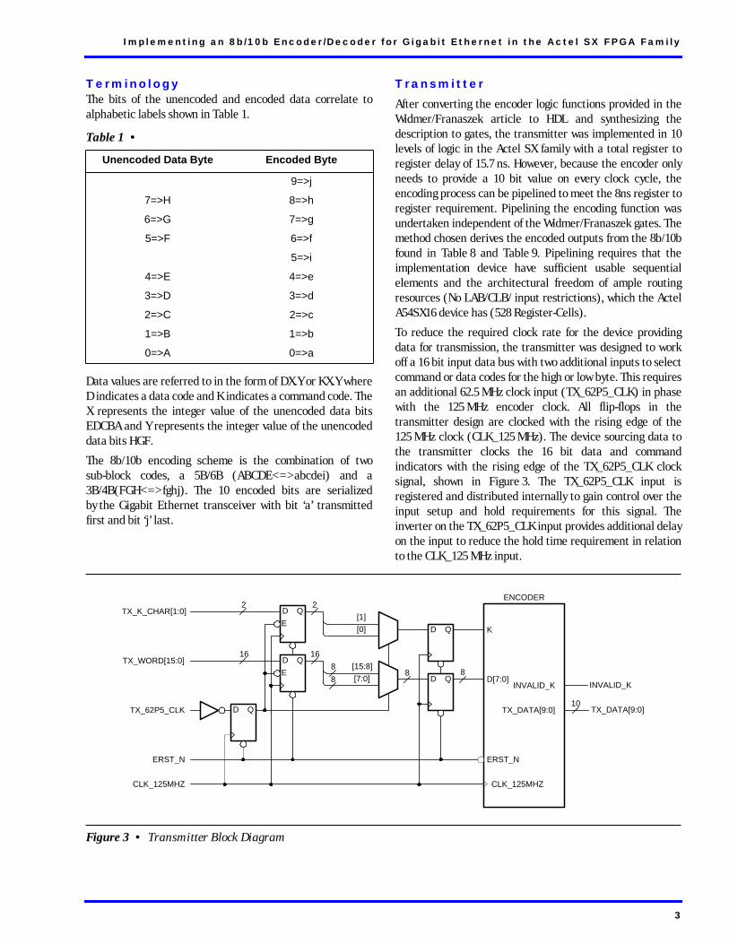
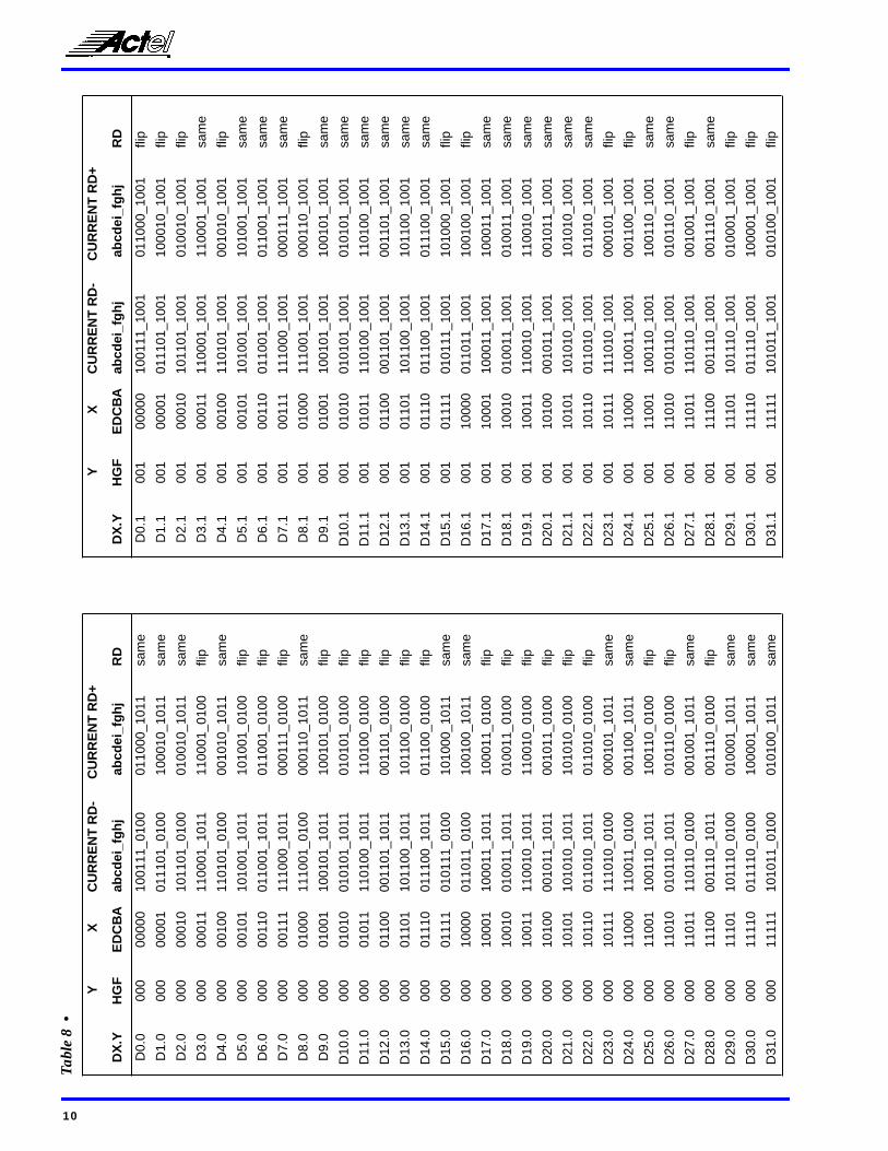
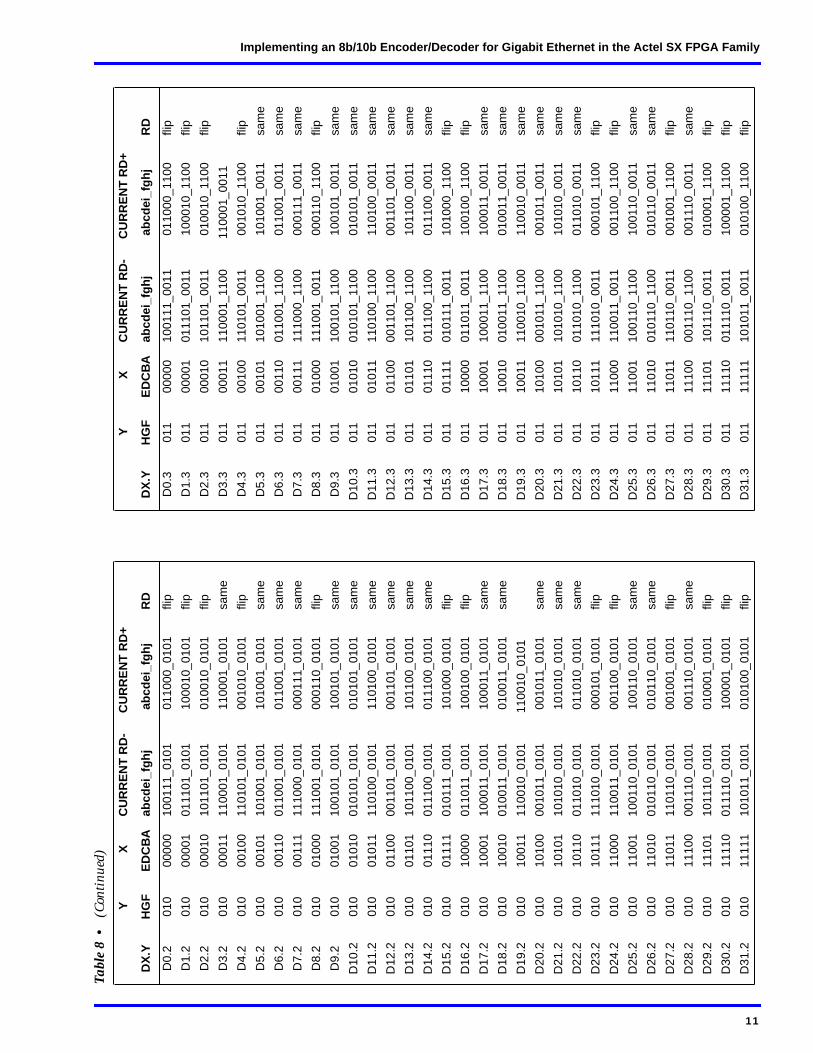
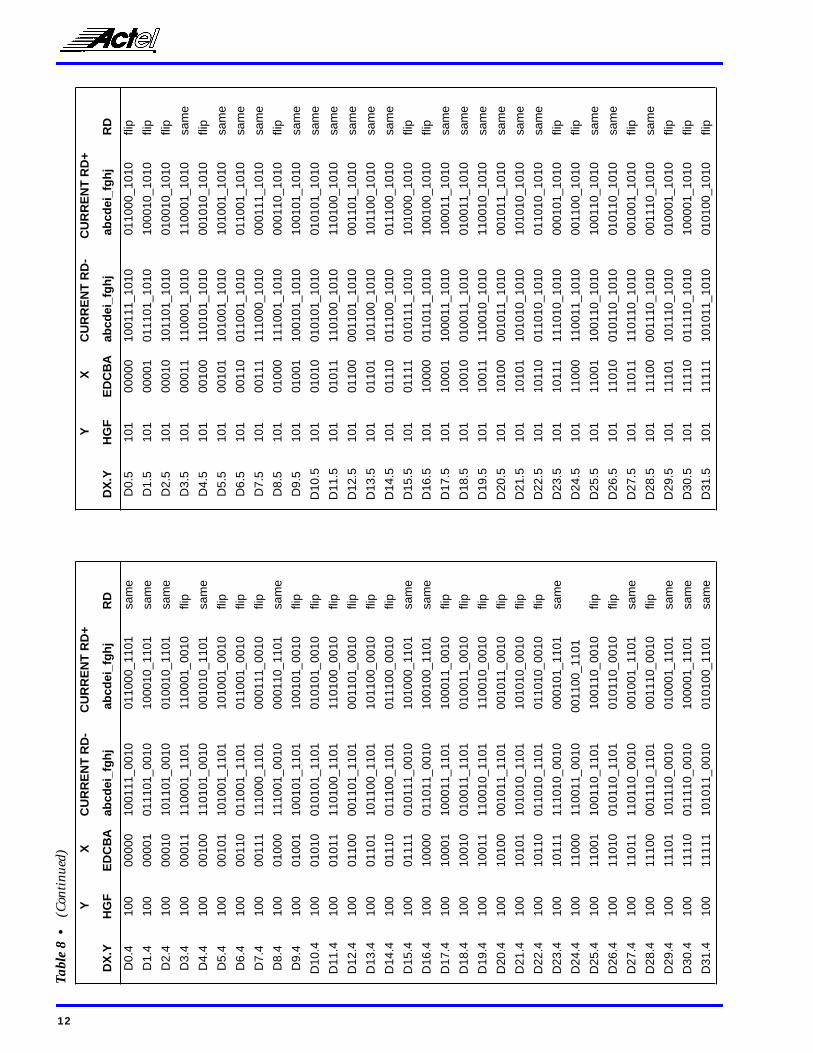
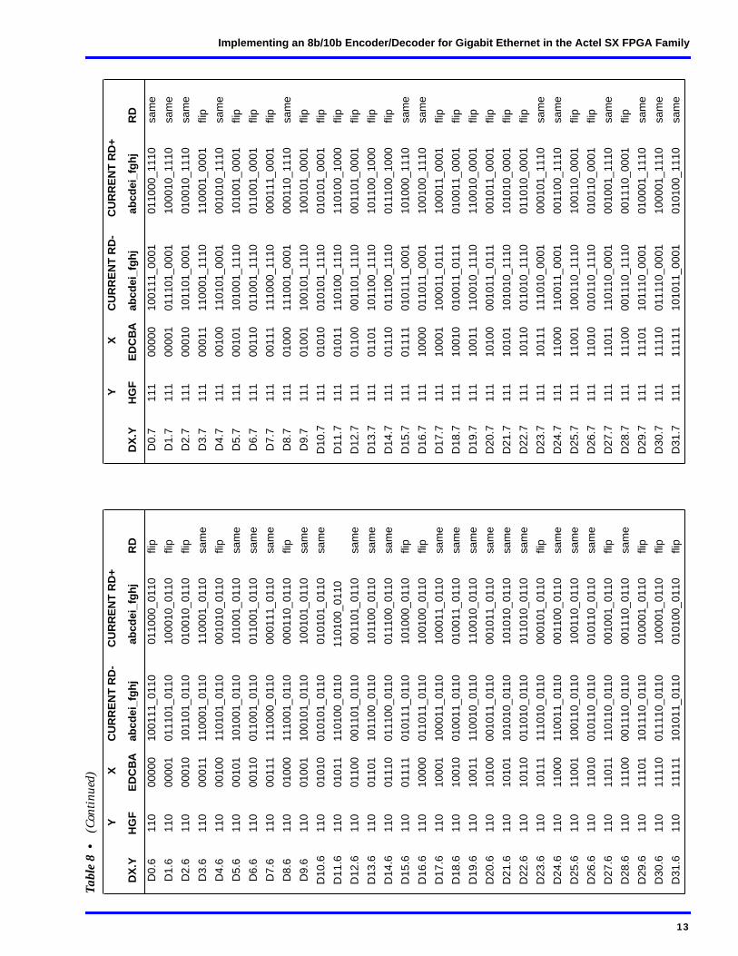
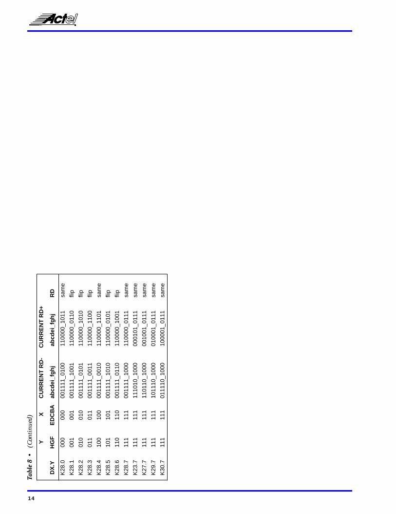
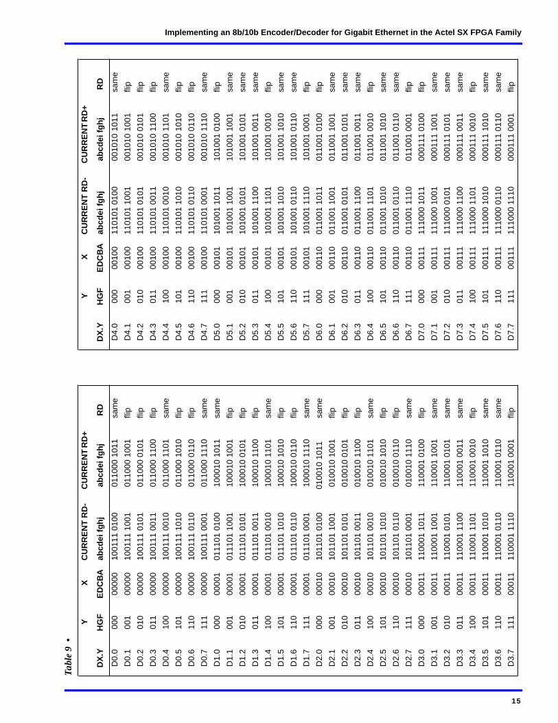
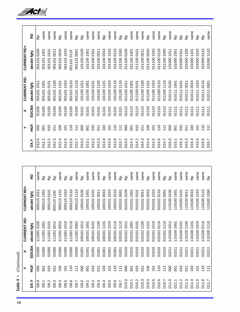
After converting the encoder logic functions provided in theWidmer/Franaszek article to HDL and synthesizing thedescription to gates, the transmitter was implemented in 10levels of logic in the Actel SX family with a total register toregister delay of 15.7 ns. However, because the encoder onlyneeds to provide a 10 bit value on every clock cycle, theencoding process can be pipelined to meet the 8ns register toregister requirement. Pipelining the encoding function wasundertaken independent of the Widmer/Franaszek gates. Themethod chosen derives the encoded outputs from the 8b/10bfound in Table 8 and Table 9. Pipelining requires that theimplementation device have sufficient usable sequentialelements and the architectural freedom of ample routingresources (No LAB/CLB/ input restrictions), which the ActelA54SX16 device has (528 Register-Cells).
To reduce the required clock rate for the device providingdata for transmission, the transmitter was designed to workoff a 16 bit input data bus with two additional inputs to selectcommand or data codes for the high or low byte. This requiresan additional 62.5 MHz clock input (TX_62P5_CLK) in phasewith the 125 MHz encoder clock. All flip-flops in thetransmitter design are clocked with the rising edge of the125 MHz clock (CLK_125 MHz). The device sourcing data tothe transmitter clocks the 16 bit data and commandindicators with the rising edge of the TX_62P5_CLK clocksignal, shown in Figure 3. The TX_62P5_CLK input isregistered and distributed internally to gain control over theinput setup and hold requirements for this signal. Theinverter on the TX_62P5_CLK input provides additional delayon the input to reduce the hold time requirement in relationto the CLK_125 MHz input.
Table 1 •
Unencoded Data Byte Encoded Byte
9=>j
7=>H 8=>h
6=>G 7=>g
5=>F 6=>f
5=>i
4=>E 4=>e
3=>D 3=>d
2=>C 2=>c
1=>B 1=>b
0=>A 0=>a
Figure 3 • Transmitter Block Diagram
D QTX_62P5_CLK
D Q
D Q
E
ETX_K_CHAR[1:0]
TX_WORD[15:0]
2
16
D Q
D Q8
ERST_N
8
CLK_125MHZ
K
D[7:0]
CLK_125MHZ
ERST_N
ENCODER
TX_DATA[9:0]
INVALID_K
10
8
8
2
16
[15:8]
[7:0]
[1]
[0]
TX_DATA[9:0]
INVALID_K
3
Encoder
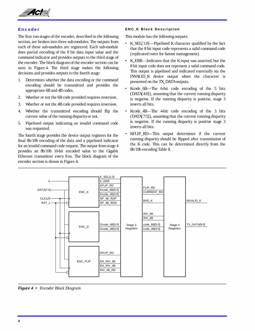
The first two stages of the encoder, described in the followingsection, are broken into three sub-modules. The outputs fromeach of these sub-modules are registered. Each sub-moduledoes partial encoding of the 8 bit data input value and thecommand indicator and provides outputs to the third stage ofthe encoder. The block diagram of the encoder section can beseen in Figure 4. The third stage makes the followingdecisions and provides outputs to the fourth stage:
1. Determines whether the data encoding or the commandencoding should be transmitted and provides theappropriate 6B and 4B codes.
2. Whether or not the 6B code provided requires inversion.
3. Whether or not the 4B code provided requires inversion.
4. Whether the transmitted encoding should flip thecurrent value of the running disparity or not.
5. Pipelined output indicating an invalid command codewas requested.
The fourth stage provides the device output registers for thefinal 8b/10b encoding of the data and a pipelined indicatorfor an invalid command code request. The output from stage 4provides an 8b/10b 10-bit encoded value to the GigabitEthernet transmitter every 8 ns. The block diagram of theencoder section is shown in Figure 4.
ENC_K Block Description
This module has the following outputs:
• K_SEL[1:0]—Pipelined K character qualified by the factthat the 8 bit input code represents a valid command code(replicated twice for fanout management).
• K_ERR—Indicates that the K input was asserted, but the8 bit input code does not represent a valid command code.This output is pipelined and indicated externally via theINVALID_K device output when the character ispresented on the TX_DATA outputs.
• Kcode_6B—The 6-bit code encoding of the 5 bits(DATA[4:0]), assuming that the current running disparityis negative. If the running disparity is positive, stage 3inverts all bits.
• Kcode_4B—The 4-bit code encoding of the 3 bits(DATA[7:5]), assuming that the current running disparityis negative. If the running disparity is positive stage 3inverts all bits.
• KFLIP_RD—This output determines if the currentrunning disparity should be flipped after transmission ofthe K code. This can be determined directly from the8b/10b encoding Table 8.
Figure 4 • Encoder Block Diagram
ENC_K
ENC_FLIP
ENC_D
DATA[7:0]
K
K_SEL[1:0]
K_ERR
KFLIP_RD
Kcode_6B[5:0]
Kcode_4B[3:0]
SP_4B_RDP
SP_4B_RDN
Dcode_6B[5:0]
Dcode_4B[3:0]
CLK125
RST_L
FLIP_RD
EN_INV_6B
EN_INV_4B
INV_4B_RD
Stage 3Registers
CURRENT_RD
Stage 4Registers
code_6B[5:0]
code_4B[3:0]
INV_6B
INV_4B
BAD_K INVALID_K
TX_DATA[9:0]
DFLIP_RD
4
Implementing an 8b/10b Encoder/Decoder for Gigabit Ethernet in the Actel SX FPGA Family
• SP_4B_RDP—Indicates one of the special 4 bit codecases when the Running Disparity (RD) is positive. If theRD is positive, the output stage forces the 4 bit code to avalue of 1000 to avoid a run length 5 code (for D codesonly, not K codes). The special data codes are D11.7,D13.7, or D14.7 when the current running disparity ispositive. See the 8b/10b encoding Table 8.
• SP_4B_RDN—Indicates one of the special 4 bit codecases when the Running Disparity (RD) is negative. If theRD is negative, the output stage forces the 4 bit code to avalue of 0111 to avoid a run length 5 code (for D codesonly, not K codes). The special data codes are D17.7,D18.7, or D20.7 when the current running disparity isnegative. See the 8b/10b encoding Table 8.
ENC_D Block Description
This module outputs one of the two pair of encodings for therespective 3 and 5 bit input values. The ENC_FLIP moduleprovides additional outputs to determine whether the outputvalue needs to be inverted or not. This can be accomplishedwith two ROM lookup tables. The first ROM table is 4 bitswide and 8 values deep (4x8) and the second ROM table is6x32. The 4x8 ROM table can use a sequential HDL casestatement with the registered version of the D[7:5] inputs asthe selector. The implementation of the 6x32 ROM table inthe Actel SX family can be done with six 32-1 multiplexors.Constant values drive the data inputs to the 32-1multiplexors. The select lines are controlled by the registeredversion of the D[4:0] inputs. The output from the multiplexoris then registered. Modeling of the larger ROM table in thisfashion forces synthesis tools to implement the larger ROMtable in a very specific manner, which should result in 3 levelsof multiplexing in the SX family.
Choosing the 4B Values for the 4x8 ROM Table
For some 3 bit input data values (1, 2, 5, and 6), the 4 bitencoding has only a single value (1001, 0101, 1010, and 0110).In addition, each of the other 3 bit input data values (0, 3, 4,and 7) have 4 bit encoding code pairs. Table 2 lists thepossible encoding values:
At this point a choice needs to be made about which of thetwo pairs to select for the 4x8 ROM table. As shown inTable 8, the transmitted 4 bit encoding depends on therunning disparity and the value of D[4:0]. The choice wasmade to place into the 4x8 ROM table the 4 bit code for the
given 3 bit data value when D[4:0] is 0000 and the runningdisparity is negative. With this selection it is possible todetermine when inversion is needed. The ENC_FLIP moduleprovides outputs used by stage 3 to determine if inversion ofthe 4B value is needed.
Choosing the 6B Values for the 6x32 ROM Table
For some 5 bit input data values (3, 5, 6, 9, 10, 11, 12, 13, 14,17, 18, 19, 20, 21, 22, 25, 26, and 28), the 6 bit encoding hasonly a single value. The other 4 bit input values have a pair ofencoding values dependent on the running disparity. Thesepairs are the inverse of one another. Table 3 lists the possibleencoding values.
Again a choice needs to be made as to which values to selectfor the 6x32 ROM table. For this discussion, the choice wasmade to place into the 6x32 ROM table the 6 bit codes,assuming that the running disparity is negative. TheENC_FLIP module provides outputs used by stage 3 todetermine if inversion of the 6B value is needed.
ENC_FLIP Block Description
This module has the following outputs:
• DFLIP_RD—This output determines if the currentrunning disparity should flip after transmission of the Dcode. This can be determined directly from the 8b/10bencoding Table 8.
• EN_INV_6B—This output is asserted for the 6B codevalues that have two pairs as noted in the sectiondiscussing the ENC_D block. It does not assert for the 6Bcode values with a single value. The third stage combinesthis output with the current running disparity todetermine if the 6B code provided by the ENC_D modulerequires inversion.
Table 2 •
0 ∞ 0100 or 1011 4 ∞ 0010 or 1101
1 ∞ 1001 5 ∞ 1010
2 ∞ 0101 6 ∞ 0110
3 ∞ 0011 or 1100 7 ∞ 0001 or 1110 ∗* D11.7, D13.7, D14.7, D17.7, D18.7, or D20.7 depending on the runningdisparity are special cases as noted in the preceding ENC_K section.
Table 3 •
0 ∞ 100111 or 011000 16 ∞ 011011 or 100100
1 ∞ 011101 or 100010 17 ∞ 100011
2 ∞ 101101 or 010010 18 ∞ 010011
3 ∞ 110001 19 ∞ 110010
4 ∞ 110101 or 001010 20 ∞ 001011
5 ∞ 101001 21 ∞ 101010
6 ∞ 011001 22 ∞ 011010
7 ∞ 111000 or 000111 23 ∞ 111010 or 000101
8 ∞ 111001or 000101 24 ∞ 110011 or 001100
9 ∞ 100101 25 ∞ 100110
10 ∞ 010101 26 ∞ 010110
11 ∞ 110100 27 ∞ 110110 or 001001
12 ∞ 001101 28 ∞ 001110
13 ∞ 101100 29 ∞ 101110 or 010001
14 ∞ 011100 30 ∞ 011110 or 100001
15 ∞ 010111 or 101000 31 ∞ 101011 or 010100
5
• EN_INV_4B—This output is asserted for the followingvalues of DATA[7:5]: 0, 3, 4, and 7. These are the 4B codevalues with two pairs. When asserted, this output indicatesone of the 4B data codes that have an alternate pair. Thethird stage uses this output to enable inversion for the 4Bdata code if INV_4B_RD and the current running disparityindicate that inversion of the 4B code provided by theENC_D module is needed.
• INV_4B_RD—This output is asserted for the followingvalues of DATA[4:0]: 0, 1, 2, 4, 8, 15, 16, 23, 24, 27, 29, 30,and 31. The third stage indicates that inversion of the 4Bdata encoding provided by the ENC_D module is requiredunder the following conditions shown in Table 4.
This is the exclusive-nor of the INV_4B_RD signal and therunning disparity.
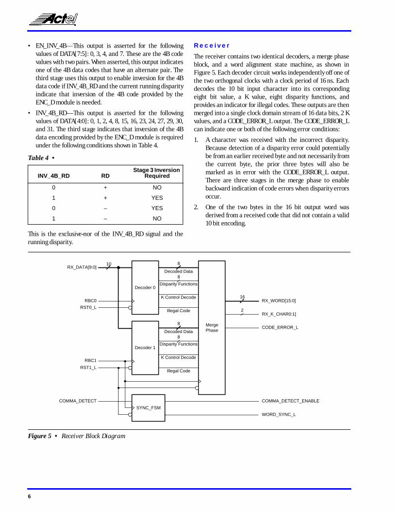
Receiver
The receiver contains two identical decoders, a merge phaseblock, and a word alignment state machine, as shown inFigure 5. Each decoder circuit works independently off one ofthe two orthogonal clocks with a clock period of 16 ns. Eachdecodes the 10 bit input character into its correspondingeight bit value, a K value, eight disparity functions, andprovides an indicator for illegal codes. These outputs are thenmerged into a single clock domain stream of 16 data bits, 2 Kvalues, and a CODE_ERROR_L output. The CODE_ERROR_Lcan indicate one or both of the following error conditions:
1. A character was received with the incorrect disparity.Because detection of a disparity error could potentiallybe from an earlier received byte and not necessarily fromthe current byte, the prior three bytes will also bemarked as in error with the CODE_ERROR_L output.There are three stages in the merge phase to enablebackward indication of code errors when disparity errorsoccur.
2. One of the two bytes in the 16 bit output word wasderived from a received code that did not contain a valid10 bit encoding.
Table 4 •
INV_4B_RD RDStage 3 Inversion
Required
0 + NO
1 + YES
0 – YES
1 – NO
Figure 5 • Receiver Block Diagram
8
8Decoded Data
Disparity Functions
K Control Decode
Illegal Code
8
8Decoded Data
Disparity Functions
K Control Decode
Illegal Code
RBC0
RBC1
16RX_WORD[15:0]
COMMA_DETECT_ENABLE
2RX_K_CHAR0:1]
MergePhase
RX_DATA[9:0]10
SYNC_FSM
COMMA_DETECT
Decoder 0
Decoder 1
RST0_L
RST1_L
CODE_ERROR_L
WORD_SYNC_L
6
Implementing an 8b/10b Encoder/Decoder for Gigabit Ethernet in the Actel SX FPGA Family
The receiver must validate that the received character hadthe correct disparity. One method of accomplishing this is topass disparity information back and forth across the RBC0and RBC1 clock domains. However, implementing the checkin this fashion would require tighter timing constraints thanthe method chosen for this discussion. Checking the runningdisparity across the two decoders was solved without havingto pass information between the two decoder clock domains.The 4 disparity function outputs from the decoder blocks areall captured with the rising edge of the RBC1 clock domain.The timing required from the registered outputs of theDecoder0 block to the registered inputs in the merge phaseblock is 8 ns, which is easily achieved and verified. Onceregistered in the merge phase block, the disparity functionsare used to validate that the two characters received have thecorrect disparity. These inputs to the merge block are alsoused to update the current running disparity for the check ofthe next word of data.
Decoder
Each of the two Decoder blocks contain input registers tocapture the 10 bits of received encoded data (RX_DATA[9:0]inputs) with their respective clock. Each decoder blockperforms four different functions; decode the 8 bit data value,calculate the 8 disparity functions, check for a commandencoding, and check for illegal codes.
Data Values
The decoded value for bits 4 through 0 depend only on theencoded bits 0 to 5. Only 48 of the possible 64 values that canbe received on bits 0 to 5 represent valid 8b/10b codes.Therefore, the decoding for bits 4 through 0 can be easilymodeled in HDL code with a case statement. The decodevalues can be determined from the 8b/10b tables found inappendices A and B.
The decode of received data bits 7 through 5 are dependenton all ten of the received bits. The decoding of received bits 6to 9 may change when bits 0 to 5 are equal to 110000, or aK28.X command encoding. Furthermore the above encodingonly affects the decoding when the received bits 6 to 9 areequal to 0101, 0110, 1001, and 1010 (K28.2, K28.1, K28.6, andK28.2 respectively). Only 14 of the possible 16 values that canbe received on bits 6 to 9 represent valid 8b/10b codes. Againthis can be modeled in HDL code with a case statement.
However, this time an “if” condition testing for the 110000condition on received bits 0 to 5 must be used when thereceived bits 6 to 9 are equal to the values listed above. Thedecode values can be determined from the 8b/10b tablesfound in appendices A and B.
Disparity Functions
There are eight disparity function outputs from each decoderblock. Four of these outputs are determined from thereceived bits 0 to 5, while the other four outputs are derivedfrom received bits 6 to 9. The following description andunderstanding of these disparity functions requires namingthem as follows: PD6BU, ND6BU, PD4BU, ND4BU, PD6BC,ND6BC, PD4BC, and ND4BC. The first four disparityfunctions determine only whether the received sub blockcode had positive or negative disparity. The last four outputsinclude the above determination plus the zero disparity casesof 000111, 111000, 0011, and 1100 respectively. The additionalcases are DC balanced and have a running disparity of 0.Disparity is updated and checked at each sub block boundary.The first four disparity functions are used to update theresulting running disparity after reception of the first 6 bitsub block code and again after the reception of the 4 bit subblock code. The last four disparity functions are used tovalidate the received code based on the current runningdisparity and the disparity of the received code.
An example proves helpful to better understand the need forthe additional cases in the last four disparity functions usedto validate the received code. Assume that the currentrunning disparity is positive and that the received 8b/10bcode has the value 111000_1001 (D7.1). A disparity violationshould be flagged. Note that the sub block code 111000 has adisparity value of zero and does not cause the current runningdisparity value to change. However, the proper code fortransmission of D7.1 when the running disparity is positive is000111_1001. The additional case of 000111 in the PD6BCfunction enables detection of this violation. The need for theadditional zero disparity cases for ND6BC, PD4BC, andND4BC can be explained a similar fashion.
Another example proves helpful in understanding whyWidmer and Franaszek made this encoding choice. Assumethat the current running disparity is negative and theconsecutive codes D20.7 and D7.1 are received with andwithout a violation, as indicated in Table 5.
Table 5 •
(RD-) D20.7 (RD+) D7.1 (RD+)
Violation (RD-) 001011 0111 (RD+) 111000 1001 (RD+)
Correct (RD-) 001011 0111 (RD+) 000111 1001 (RD+)
7
If the encoding of the 6 bit sub block for X=7 is 111000, as inthe violation case above, a run length of six ‘1’s results. Thisviolates the 8b/10b encoding scheme’s maximum run lengthlimit of 5. Therefore, the encoding of X=7 when the currentrunning disparity is positive was chosen to be 000111.Similarly, the correct value is 111000 when the currentrunning disparity is negative.
To understand the 4 bit sub block encoding choice for Y=3,examine the encoding of the K28.3 character. The correctencoding is 001111_0011 when the running disparity isnegative and 110000_1100 when positive. If the oppositechoice of 1100 and 0011 had been made for Y=3, a run lengthof six ‘1’s or six ‘0’s would result.
Command Code Checking
Each decoder has a single output to indicate that the 10 bitreceived code was a command character. The followingencodings are unique to command codes:
Each decoder has a single output to indicate that the 10 bitreceived code was a command character. The followingencodings are unique to command codes:
• K28.X with positive running disparity indicated by bits 5 to2 equal to 0000.
• K28.X with negative running disparity indicated by bits 5to 2 equal to 1111.
• K23.7, K27.7 and K30.7 with positive running disparityindicated by bits 9 to 4 equal to 010111 and one single bitin 3 to 0 equal to ‘1’ with all others equal to ‘0’.
• K23.7, K27.7 and K30.7 with negative running disparityindicated by bits 9 to 4 equal to 101000 and one single bitin 3 to 0 equal to ‘0’ with all others equal to ‘1’.
Invalid Code Checking
The invalid code violation equations are taken directly fromthe Widmer/Franaszek article with two additions. The two8b/10b codes 001111_0001 and 110000_1110 are not coveredby the equations and they do not cause running disparityerrors. Therefore, these two code checks have been added.The following conditions are violations of the coding rulesand cause the output of Illegal_Code to be asserted:
• a = b = c = d
• P13 & !e & !i
• P31 & e & i
• f = g = h = j
• e = i = f = g = h
• i != e = g = h = j
• (e = i != g = h = j) & !(c = d = e)
• !P31 & e & !i & !g & !h & !j
• !P13 & !e & i & g & h & j
• !a & !b & c & d & e & i & !f & !g & !h & i
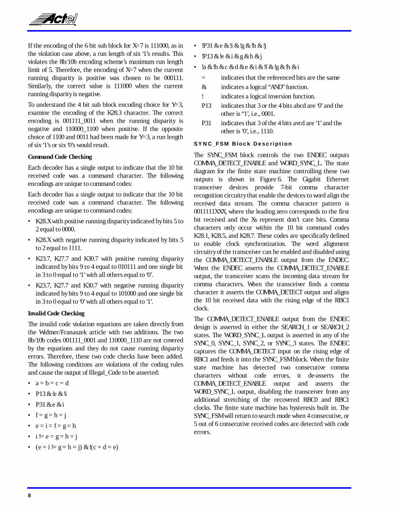
SYNC_FSM Block Description
The SYNC_FSM block controls the two ENDEC outputsCOMMA_DETECT_ENABLE and WORD_SYNC_L. The statediagram for the finite state machine controlling these twooutputs is shown in Figure 6. The Gigabit Ethernettransceiver devices provide 7-bit comma characterrecognition circuitry that enable the devices to word align thereceived data stream. The comma character pattern is0011111XXX, where the leading zero corresponds to the firstbit received and the Xs represent don’t care bits. Commacharacters only occur within the 10 bit command codesK28.1, K28.5, and K28.7. These codes are specifically definedto enable clock synchronization. The word alignmentcircuitry of the transceiver can be enabled and disabled usingthe COMMA_DETECT_ENABLE output from the ENDEC.When the ENDEC asserts the COMMA_DETECT_ENABLEoutput, the transceiver scans the incoming data stream forcomma characters. When the transceiver finds a commacharacter it asserts the COMMA_DETECT output and alignsthe 10 bit received data with the rising edge of the RBC1clock.
The COMMA_DETECT_ENABLE output from the ENDECdesign is asserted in either the SEARCH_1 or SEARCH_2states. The WORD_SYNC_L output is asserted in any of theSYNC_0, SYNC_1, SYNC_2, or SYNC_3 states. The ENDECcaptures the COMMA_DETECT input on the rising edge ofRBC1 and feeds it into the SYNC_FSM block. When the finitestate machine has detected two consecutive commacharacters without code errors, it de-asserts theCOMMA_DETECT_ENABLE output and asserts theWORD_SYNC_L output, disabling the transceiver from anyadditional stretching of the recovered RBC0 and RBC1clocks. The finite state machine has hysteresis built in. TheSYNC_FSM will return to search mode when 4 consecutive, or5 out of 6 consecutive received codes are detected with codeerrors.
= indicates that the referenced bits are the same& indicates a logical “AND” function.! indicates a logical inversion function.P13 indicates that 3 or the 4 bits abcd are ‘0’ and the
other is “1’, i.e., 0001.P31 indicates that 3 of the 4 bits avcd are ‘1’ and the
other is ‘0’, i.e., 1110.
8
Implementing an 8b/10b Encoder/Decoder for Gigabit Ethernet in the Actel SX FPGA Family
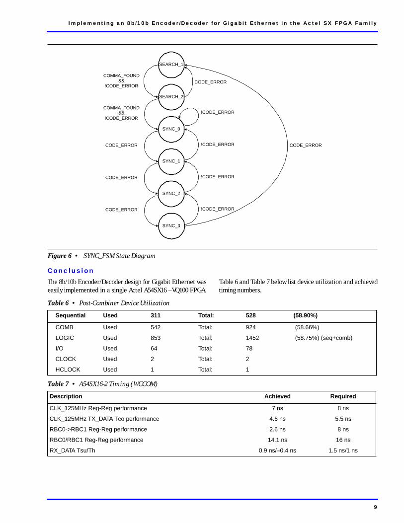
Conclusion
The 8b/10b Encoder/Decoder design for Gigabit Ethernet waseasily implemented in a single Actel A54SX16 –VQ100 FPGA.
Table 6 and Table 7 below list device utilization and achievedtiming numbers.
Figure 6 • SYNC_FSM State Diagram
SEARCH_1
SEARCH_2
SYNC_0
SYNC_1
SYNC_2
SYNC_3
COMMA_FOUND&&
!CODE_ERROR
COMMA_FOUND&&
!CODE_ERROR
CODE_ERROR
CODE_ERROR
!CODE_ERROR
!CODE_ERROR
!CODE_ERROR
CODE_ERROR
CODE_ERROR
CODE_ERROR
!CODE_ERROR
Table 6 • Post-Combiner Device Utilization
Sequential Used 311 Total: 528 (58.90%)
COMB Used 542 Total: 924 (58.66%)
LOGIC Used 853 Total: 1452 (58.75%) (seq+comb)
I/O Used 64 Total: 78
CLOCK Used 2 Total: 2
HCLOCK Used 1 Total: 1
Table 7 • A54SX16-2 Timing (WCCOM)
Description Achieved Required
CLK_125MHz Reg-Reg performance 7 ns 8 ns
CLK_125MHz TX_DATA Tco performance 4.6 ns 5.5 ns
RBC0->RBC1 Reg-Reg performance 2.6 ns 8 ns
RBC0/RBC1 Reg-Reg performance 14.1 ns 16 ns
RX_DATA Tsu/Th 0.9 ns/–0.4 ns 1.5 ns/1 ns
9
Tabl
e 8
•
Y
X
CU
RR
EN
T R
D-
CU
RR
EN
T R
D+
Y
X
CU
RR
EN
T R
D-
CU
RR
EN
T R
D+
DX
.YH
GF
ED
CB
Aab
cdei
_fgh
j a
bcde
i_fg
hjR
DD
X.Y
HG
FE
DC
BA
abcd
ei_f
ghj
abc
dei_
fghj
RD
D0.
000
000
000
1001
11_0
100
011
000_
1011
sam
e
D0.
100
100
000
1001
11_1
001
011
000_
1001
flip
D1.
000
000
001
0111
01_0
100
100
010_
1011
sam
e
D1.
100
100
001
0111
01_1
001
100
010_
1001
flip
D2.
000
000
010
1011
01_0
100
010
010_
1011
sam
e
D2.
100
100
010
1011
01_1
001
010
010_
1001
flip
D3.
000
000
011
1100
01_1
011
110
001_
0100
flip
D
3.1
001
0001
111
0001
_100
1 1
1000
1_10
01sa
me
D4.
000
000
100
1101
01_0
100
001
010_
1011
sam
e
D4.
100
100
100
1101
01_1
001
001
010_
1001
flip
D5.
000
000
101
1010
01_1
011
101
001_
0100
flip
D
5.1
001
0010
110
1001
_100
1 1
0100
1_10
01sa
me
D6.
000
000
110
0110
01_1
011
011
001_
0100
flip
D
6.1
001
0011
001
1001
_100
1 0
1100
1_10
01sa
me
D7.
000
000
111
1110
00_1
011
000
111_
0100
flip
D
7.1
001
0011
111
1000
_100
1 0
0011
1_10
01sa
me
D8.
000
001
000
1110
01_0
100
000
110_
1011
sam
e
D8.
100
101
000
1110
01_1
001
000
110_
1001
flip
D9.
000
001
001
1001
01_1
011
100
101_
0100
flip
D
9.1
001
0100
110
0101
_100
1 1
0010
1_10
01sa
me
D10
.000
001
010
0101
01_1
011
010
101_
0100
flip
D
10.1
001
0101
001
0101
_100
1 0
1010
1_10
01sa
me
D11
.000
001
011
1101
00_1
011
110
100_
0100
flip
D
11.1
001
0101
111
0100
_100
1 1
1010
0_10
01sa
me
D12
.000
001
100
0011
01_1
011
001
101_
0100
flip
D
12.1
001
0110
000
1101
_100
1 0
0110
1_10
01sa
me
D13
.000
001
101
1011
00_1
011
101
100_
0100
flip
D
13.1
001
0110
110
1100
_100
1 1
0110
0_10
01sa
me
D14
.000
001
110
0111
00_1
011
011
100_
0100
flip
D
14.1
001
0111
001
1100
_100
1 0
1110
0_10
01sa
me
D15
.000
001
111
0101
11_0
100
101
000_
1011
sam
e
D15
.100
101
111
0101
11_1
001
101
000_
1001
flip
D16
.000
010
000
0110
11_0
100
100
100_
1011
sam
e
D16
.100
110
000
0110
11_1
001
100
100_
1001
flip
D17
.000
010
001
1000
11_1
011
100
011_
0100
flip
D
17.1
001
1000
110
0011
_100
1 1
0001
1_10
01sa
me
D18
.000
010
010
0100
11_1
011
010
011_
0100
flip
D
18.1
001
1001
001
0011
_100
1 0
1001
1_10
01sa
me
D19
.000
010
011
1100
10_1
011
110
010_
0100
flip
D
19.1
001
1001
111
0010
_100
1 1
1001
0_10
01sa
me
D20
.000
010
100
0010
11_1
011
001
011_
0100
flip
D
20.1
001
1010
000
1011
_100
1 0
0101
1_10
01sa
me
D21
.000
010
101
1010
10_1
011
101
010_
0100
flip
D
21.1
001
1010
110
1010
_100
1 1
0101
0_10
01sa
me
D22
.000
010
110
0110
10_1
011
011
010_
0100
flip
D
22.1
001
1011
001
1010
_100
1 0
1101
0_10
01sa
me
D23
.000
010
111
1110
10_0
100
000
101_
1011
sam
e
D23
.100
110
111
1110
10_1
001
000
101_
1001
flip
D24
.000
011
000
1100
11_0
100
001
100_
1011
sam
e
D24
.100
111
000
1100
11_1
001
001
100_
1001
flip
D25
.000
011
001
1001
10_1
011
100
110_
0100
flip
D
25.1
001
1100
110
0110
_100
1 1
0011
0_10
01sa
me
D26
.000
011
010
0101
10_1
011
010
110_
0100
flip
D
26.1
001
1101
001
0110
_100
1 0
1011
0_10
01sa
me
D27
.000
011
011
1101
10_0
100
001
001_
1011
sam
e
D27
.100
111
011
1101
10_1
001
001
001_
1001
flip
D28
.000
011
100
0011
10_1
011
001
110_
0100
flip
D
28.1
001
1110
000
1110
_100
1 0
0111
0_10
01sa
me
D29
.000
011
101
1011
10_0
100
010
001_
1011
sam
e
D29
.100
111
101
1011
10_1
001
010
001_
1001
flip
D30
.000
011
110
0111
10_0
100
100
001_
1011
sam
e
D30
.100
111
110
0111
10_1
001
100
001_
1001
flip
D31
.000
011
111
1010
11_0
100
010
100_
1011
sam
e
D31
.100
111
111
1010
11_1
001
010
100_
1001
flip
10
Implementing an 8b/10b Encoder/Decoder for Gigabit Ethernet in the Actel SX FPGA Family
D0.
201
000
000
1001
11_0
101
011
000_
0101
flip
D
0.3
011
0000
010
0111
_001
1 0
1100
0_11
00fli
p
D1.
201
000
001
0111
01_0
101
100
010_
0101
flip
D
1.3
011
0000
101
1101
_001
1 1
0001
0_11
00fli
p
D2.
201
000
010
1011
01_0
101
010
010_
0101
flip
D
2.3
011
0001
010
1101
_001
1 0
1001
0_11
00fli
p
D3.
201
000
011
1100
01_0
101
110
001_
0101
sam
e
D3.
301
100
011
1100
01_1
100
1100
01_0
011
D4.
201
000
100
1101
01_0
101
001
010_
0101
flip
D
4.3
011
0010
011
0101
_001
1 0
0101
0_11
00fli
p
D5.
201
000
101
1010
01_0
101
101
001_
0101
sam
e
D5.
301
100
101
1010
01_1
100
101
001_
0011
sam
e
D6.
201
000
110
0110
01_0
101
011
001_
0101
sam
e
D6.
301
100
110
0110
01_1
100
011
001_
0011
sam
e
D7.
201
000
111
1110
00_0
101
000
111_
0101
sam
e
D7.
301
100
111
1110
00_1
100
000
111_
0011
sam
e
D8.
201
001
000
1110
01_0
101
000
110_
0101
flip
D
8.3
011
0100
011
1001
_001
1 0
0011
0_11
00fli
p
D9.
201
001
001
1001
01_0
101
100
101_
0101
sam
e
D9.
301
101
001
1001
01_1
100
100
101_
0011
sam
e
D10
.201
001
010
0101
01_0
101
010
101_
0101
sam
e
D10
.301
101
010
0101
01_1
100
010
101_
0011
sam
e
D11
.201
001
011
1101
00_0
101
110
100_
0101
sam
e
D11
.301
101
011
1101
00_1
100
110
100_
0011
sam
e
D12
.201
001
100
0011
01_0
101
001
101_
0101
sam
e
D12
.301
101
100
0011
01_1
100
001
101_
0011
sam
e
D13
.201
001
101
1011
00_0
101
101
100_
0101
sam
e
D13
.301
101
101
1011
00_1
100
101
100_
0011
sam
e
D14
.201
001
110
0111
00_0
101
011
100_
0101
sam
e
D14
.301
101
110
0111
00_1
100
011
100_
0011
sam
e
D15
.201
001
111
0101
11_0
101
101
000_
0101
flip
D
15.3
011
0111
101
0111
_001
1 1
0100
0_11
00fli
p
D16
.201
010
000
0110
11_0
101
100
100_
0101
flip
D
16.3
011
1000
001
1011
_001
1 1
0010
0_11
00fli
p
D17
.201
010
001
1000
11_0
101
100
011_
0101
sam
e
D17
.301
110
001
1000
11_1
100
100
011_
0011
sam
e
D18
.201
010
010
0100
11_0
101
010
011_
0101
sam
e
D18
.301
110
010
0100
11_1
100
010
011_
0011
sam
e
D19
.201
010
011
1100
10_0
101
1100
10_0
101
D19
.301
110
011
1100
10_1
100
110
010_
0011
sam
e
D20
.201
010
100
0010
11_0
101
001
011_
0101
sam
e
D20
.301
110
100
0010
11_1
100
001
011_
0011
sam
e
D21
.201
010
101
1010
10_0
101
101
010_
0101
sam
e
D21
.301
110
101
1010
10_1
100
101
010_
0011
sam
e
D22
.201
010
110
0110
10_0
101
011
010_
0101
sam
e
D22
.301
110
110
0110
10_1
100
011
010_
0011
sam
e
D23
.201
010
111
1110
10_0
101
000
101_
0101
flip
D
23.3
011
1011
111
1010
_001
1 0
0010
1_11
00fli
p
D24
.201
011
000
1100
11_0
101
001
100_
0101
flip
D
24.3
011
1100
011
0011
_001
1 0
0110
0_11
00fli
p
D25
.201
011
001
1001
10_0
101
100
110_
0101
sam
e
D25
.301
111
001
1001
10_1
100
100
110_
0011
sam
e
D26
.201
011
010
0101
10_0
101
010
110_
0101
sam
e
D26
.301
111
010
0101
10_1
100
010
110_
0011
sam
e
D27
.201
011
011
1101
10_0
101
001
001_
0101
flip
D
27.3
011
1101
111
0110
_001
1 0
0100
1_11
00fli
p
D28
.201
011
100
0011
10_0
101
001
110_
0101
sam
e
D28
.301
111
100
0011
10_1
100
001
110_
0011
sam
e
D29
.201
011
101
1011
10_0
101
010
001_
0101
flip
D
29.3
011
1110
110
1110
_001
1 0
1000
1_11
00fli
p
D30
.201
011
110
0111
10_0
101
100
001_
0101
flip
D
30.3
011
1111
001
1110
_001
1 1
0000
1_11
00fli
p
D31
.201
011
111
1010
11_0
101
010
100_
0101
flip
D
31.3
011
1111
110
1011
_001
1 0
1010
0_11
00fli
p
Tabl
e 8
• (
Cont
inue
d)
Y
X
CU
RR
EN
T R
D-
CU
RR
EN
T R
D+
Y
X
CU
RR
EN
T R
D-
CU
RR
EN
T R
D+
DX
.YH
GF
ED
CB
Aab
cdei
_fgh
j a
bcde
i_fg
hjR
DD
X.Y
HG
FE
DC
BA
abcd
ei_f
ghj
abc
dei_
fghj
RD
11
D0.
410
000
000
1001
11_0
010
011
000_
1101
sam
e
D0.
510
100
000
1001
11_1
010
011
000_
1010
flip
D1.
410
000
001
0111
01_0
010
100
010_
1101
sam
e
D1.
510
100
001
0111
01_1
010
100
010_
1010
flip
D2.
410
000
010
1011
01_0
010
010
010_
1101
sam
e
D2.
510
100
010
1011
01_1
010
010
010_
1010
flip
D3.
410
000
011
1100
01_1
101
110
001_
0010
flip
D
3.5
101
0001
111
0001
_101
0 1
1000
1_10
10sa
me
D4.
410
000
100
1101
01_0
010
001
010_
1101
sam
e
D4.
510
100
100
1101
01_1
010
001
010_
1010
flip
D5.
410
000
101
1010
01_1
101
101
001_
0010
flip
D
5.5
101
0010
110
1001
_101
0 1
0100
1_10
10sa
me
D6.
410
000
110
0110
01_1
101
011
001_
0010
flip
D
6.5
101
0011
001
1001
_101
0 0
1100
1_10
10sa
me
D7.
410
000
111
1110
00_1
101
000
111_
0010
flip
D
7.5
101
0011
111
1000
_101
0 0
0011
1_10
10sa
me
D8.
410
001
000
1110
01_0
010
000
110_
1101
sam
e
D8.
510
101
000
1110
01_1
010
000
110_
1010
flip
D9.
410
001
001
1001
01_1
101
100
101_
0010
flip
D
9.5
101
0100
110
0101
_101
0 1
0010
1_10
10sa
me
D10
.410
001
010
0101
01_1
101
010
101_
0010
flip
D
10.5
101
0101
001
0101
_101
0 0
1010
1_10
10sa
me
D11
.410
001
011
1101
00_1
101
110
100_
0010
flip
D
11.5
101
0101
111
0100
_101
0 1
1010
0_10
10sa
me
D12
.410
001
100
0011
01_1
101
001
101_
0010
flip
D
12.5
101
0110
000
1101
_101
0 0
0110
1_10
10sa
me
D13
.410
001
101
1011
00_1
101
101
100_
0010
flip
D
13.5
101
0110
110
1100
_101
0 1
0110
0_10
10sa
me
D14
.410
001
110
0111
00_1
101
011
100_
0010
flip
D
14.5
101
0111
001
1100
_101
0 0
1110
0_10
10sa
me
D15
.410
001
111
0101
11_0
010
101
000_
1101
sam
e
D15
.510
101
111
0101
11_1
010
101
000_
1010
flip
D16
.410
010
000
0110
11_0
010
100
100_
1101
sam
e
D16
.510
110
000
0110
11_1
010
100
100_
1010
flip
D17
.410
010
001
1000
11_1
101
100
011_
0010
flip
D
17.5
101
1000
110
0011
_101
0 1
0001
1_10
10sa
me
D18
.410
010
010
0100
11_1
101
010
011_
0010
flip
D
18.5
101
1001
001
0011
_101
0 0
1001
1_10
10sa
me
D19
.410
010
011
1100
10_1
101
110
010_
0010
flip
D
19.5
101
1001
111
0010
_101
0 1
1001
0_10
10sa
me
D20
.410
010
100
0010
11_1
101
001
011_
0010
flip
D
20.5
101
1010
000
1011
_101
0 0
0101
1_10
10sa
me
D21
.410
010
101
1010
10_1
101
101
010_
0010
flip
D
21.5
101
1010
110
1010
_101
0 1
0101
0_10
10sa
me
D22
.410
010
110
0110
10_1
101
011
010_
0010
flip
D
22.5
101
1011
001
1010
_101
0 0
1101
0_10
10sa
me
D23
.410
010
111
1110
10_0
010
000
101_
1101
sam
e
D23
.510
110
111
1110
10_1
010
000
101_
1010
flip
D24
.410
011
000
1100
11_0
010
0011
00_1
101
D24
.510
111
000
1100
11_1
010
001
100_
1010
flip
D25
.410
011
001
1001
10_1
101
100
110_
0010
flip
D
25.5
101
1100
110
0110
_101
0 1
0011
0_10
10sa
me
D26
.410
011
010
0101
10_1
101
010
110_
0010
flip
D
26.5
101
1101
001
0110
_101
0 0
1011
0_10
10sa
me
D27
.410
011
011
1101
10_0
010
001
001_
1101
sam
e
D27
.510
111
011
1101
10_1
010
001
001_
1010
flip
D28
.410
011
100
0011
10_1
101
001
110_
0010
flip
D
28.5
101
1110
000
1110
_101
0 0
0111
0_10
10sa
me
D29
.410
011
101
1011
10_0
010
010
001_
1101
sam
e
D29
.510
111
101
1011
10_1
010
010
001_
1010
flip
D30
.410
011
110
0111
10_0
010
100
001_
1101
sam
e
D30
.510
111
110
0111
10_1
010
100
001_
1010
flip
D31
.410
011
111
1010
11_0
010
010
100_
1101
sam
e
D31
.510
111
111
1010
11_1
010
010
100_
1010
flip
Tabl
e 8
• (
Cont
inue
d)
Y
X
CU
RR
EN
T R
D-
CU
RR
EN
T R
D+
Y
X
CU
RR
EN
T R
D-
CU
RR
EN
T R
D+
DX
.YH
GF
ED
CB
Aab
cdei
_fgh
j a
bcde
i_fg
hjR
DD
X.Y
HG
FE
DC
BA
abcd
ei_f
ghj
abc
dei_
fghj
RD
12
Implementing an 8b/10b Encoder/Decoder for Gigabit Ethernet in the Actel SX FPGA Family
D0.
611
000
000
1001
11_0
110
011
000_
0110
flip
D
0.7
111
0000
010
0111
_000
1 0
1100
0_11
10sa
me
D1.
611
000
001
0111
01_0
110
100
010_
0110
flip
D
1.7
111
0000
101
1101
_000
1 1
0001
0_11
10sa
me
D2.
611
000
010
1011
01_0
110
010
010_
0110
flip
D
2.7
111
0001
010
1101
_000
1 0
1001
0_11
10sa
me
D3.
611
000
011
1100
01_0
110
110
001_
0110
sam
e
D3.
711
100
011
1100
01_1
110
110
001_
0001
flip
D4.
611
000
100
1101
01_0
110
001
010_
0110
flip
D
4.7
111
0010
011
0101
_000
1 0
0101
0_11
10sa
me
D5.
611
000
101
1010
01_0
110
101
001_
0110
sam
e
D5.
711
100
101
1010
01_1
110
101
001_
0001
flip
D6.
611
000
110
0110
01_0
110
011
001_
0110
sam
e
D6.
711
100
110
0110
01_1
110
011
001_
0001
flip
D7.
611
000
111
1110
00_0
110
000
111_
0110
sam
e
D7.
711
100
111
1110
00_1
110
000
111_
0001
flip
D8.
611
001
000
1110
01_0
110
000
110_
0110
flip
D
8.7
111
0100
011
1001
_000
1 0
0011
0_11
10sa
me
D9.
611
001
001
1001
01_0
110
100
101_
0110
sam
e
D9.
711
101
001
1001
01_1
110
100
101_
0001
flip
D10
.611
001
010
0101
01_0
110
010
101_
0110
sam
e
D10
.711
101
010
0101
01_1
110
010
101_
0001
flip
D11
.611
001
011
1101
00_0
110
1101
00_0
110
D11
.711
101
011
1101
00_1
110
110
100_
1000
flip
D12
.611
001
100
0011
01_0
110
001
101_
0110
sam
e
D12
.711
101
100
0011
01_1
110
001
101_
0001
flip
D13
.611
001
101
1011
00_0
110
101
100_
0110
sam
e
D13
.711
101
101
1011
00_1
110
101
100_
1000
flip
D14
.611
001
110
0111
00_0
110
011
100_
0110
sam
e
D14
.711
101
110
0111
00_1
110
011
100_
1000
flip
D15
.611
001
111
0101
11_0
110
101
000_
0110
flip
D
15.7
111
0111
101
0111
_000
1 1
0100
0_11
10sa
me
D16
.611
010
000
0110
11_0
110
100
100_
0110
flip
D
16.7
111
1000
001
1011
_000
1 1
0010
0_11
10sa
me
D17
.611
010
001
1000
11_0
110
100
011_
0110
sam
e
D17
.711
110
001
1000
11_0
111
100
011_
0001
flip
D18
.611
010
010
0100
11_0
110
010
011_
0110
sam
e
D18
.711
110
010
0100
11_0
111
010
011_
0001
flip
D19
.611
010
011
1100
10_0
110
110
010_
0110
sam
e
D19
.711
110
011
1100
10_1
110
110
010_
0001
flip
D20
.611
010
100
0010
11_0
110
001
011_
0110
sam
e
D20
.711
110
100
0010
11_0
111
001
011_
0001
flip
D21
.611
010
101
1010
10_0
110
101
010_
0110
sam
e
D21
.711
110
101
1010
10_1
110
101
010_
0001
flip
D22
.611
010
110
0110
10_0
110
011
010_
0110
sam
e
D22
.711
110
110
0110
10_1
110
011
010_
0001
flip
D23
.611
010
111
1110
10_0
110
000
101_
0110
flip
D
23.7
111
1011
111
1010
_000
1 0
0010
1_11
10sa
me
D24
.611
011
000
1100
11_0
110
001
100_
0110
sam
e
D24
.711
111
000
1100
11_0
001
001
100_
1110
sam
e
D25
.611
011
001
1001
10_0
110
100
110_
0110
sam
e
D25
.711
111
001
1001
10_1
110
100
110_
0001
flip
D26
.611
011
010
0101
10_0
110
010
110_
0110
sam
e
D26
.711
111
010
0101
10_1
110
010
110_
0001
flip
D27
.611
011
011
1101
10_0
110
001
001_
0110
flip
D
27.7
111
1101
111
0110
_000
1 0
0100
1_11
10sa
me
D28
.611
011
100
0011
10_0
110
001
110_
0110
sam
e
D28
.711
111
100
0011
10_1
110
001
110_
0001
flip
D29
.611
011
101
1011
10_0
110
010
001_
0110
flip
D
29.7
111
1110
110
1110
_000
1 0
1000
1_11
10sa
me
D30
.611
011
110
0111
10_0
110
100
001_
0110
flip
D
30.7
111
1111
001
1110
_000
1 1
0000
1_11
10sa
me
D31
.611
011
111
1010
11_0
110
010
100_
0110
flip
D
31.7
111
1111
110
1011
_000
1 0
1010
0_11
10sa
me
Tabl
e 8
• (
Cont
inue
d)
Y
X
CU
RR
EN
T R
D-
CU
RR
EN
T R
D+
Y
X
CU
RR
EN
T R
D-
CU
RR
EN
T R
D+
DX
.YH
GF
ED
CB
Aab
cdei
_fgh
j a
bcde
i_fg
hjR
DD
X.Y
HG
FE
DC
BA
abcd
ei_f
ghj
abc
dei_
fghj
RD
13
K28
.000
000
000
1111
_010
0 1
1000
0_10
11sa
me
K28
.100
100
100
1111
_100
1 1
1000
0_01
10fli
p
K28
.201
001
000
1111
_010
1 1
1000
0_10
10fli
p
K28
.301
101
100
1111
_001
1 1
1000
0_11
00fli
p
K28
.410
010
000
1111
_001
0 1
1000
0_11
01sa
me
K28
.510
110
100
1111
_101
0 1
1000
0_01
01fli
p
K28
.611
011
000
1111
_011
0 1
1000
0_10
01fli
p
K28
.711
111
100
1111
_100
0 1
1000
0_01
11sa
me
K23
.711
111
111
1010
_100
0 0
0010
1_01
11sa
me
K27
.711
111
111
0110
_100
0 0
0100
1_01
11sa
me
K29
.711
111
110
1110
_100
0 0
1000
1_01
11sa
me
K30
.711
111
101
1110
_100
0 1
0000
1_01
11sa
me
Tabl
e 8
• (
Cont
inue
d)
Y
X
CU
RR
EN
T R
D-
CU
RR
EN
T R
D+
Y
X
CU
RR
EN
T R
D-
CU
RR
EN
T R
D+
DX
.YH
GF
ED
CB
Aab
cdei
_fgh
j a
bcde
i_fg
hjR
DD
X.Y
HG
FE
DC
BA
abcd
ei_f
ghj
abc
dei_
fghj
RD
14
Implementing an 8b/10b Encoder/Decoder for Gigabit Ethernet in the Actel SX FPGA Family
Tabl
e 9
•
Y
X
CU
RR
EN
T R
D-
CU
RR
EN
T R
D+
Y
X
CU
RR
EN
T R
D-
CU
RR
EN
T R
D+
DX
.YH
GF
ED
CB
Aab
cdei
fghj
abc
dei f
ghj
RD
D
X.Y
HG
FE
DC
BA
abcd
ei fg
hj a
bcde
i fgh
j R
D
D0.
000
000
000
1001
11 0
100
011
000
1011
sam
eD
4.0
000
0010
011
0101
010
0 0
0101
0 10
11sa
me
D0.
100
100
000
1001
11 1
001
011
000
1001
flip
D4.
100
100
100
1101
01 1
001
001
010
1001
flip
D0.
201
000
000
1001
11 0
101
011
000
0101
flip
D4.
201
000
100
1101
01 0
101
001
010
0101
flip
D0.
301
100
000
1001
11 0
011
011
000
1100
flip
D4.
301
100
100
1101
01 0
011
001
010
1100
flip
D0.
410
000
000
1001
11 0
010
011
000
1101
sam
eD
4.4
100
0010
011
0101
001
0 0
0101
0 11
01sa
me
D0.
510
100
000
1001
11 1
010
011
000
1010
flip
D4.
510
100
100
1101
01 1
010
001
010
1010
flip
D0.
611
000
000
1001
11 0
110
011
000
0110
flip
D4.
611
000
100
1101
01 0
110
001
010
0110
flip
D0.
711
100
000
1001
11 0
001
011
000
1110
sam
eD
4.7
111
0010
011
0101
000
1 0
0101
0 11
10sa
me
D1.
000
000
001
0111
01 0
100
100
010
1011
sam
eD
5.0
000
0010
110
1001
101
1 1
0100
1 01
00fli
p
D1.
100
100
001
0111
01 1
001
100
010
1001
flip
D5.
100
100
101
1010
01 1
001
101
001
1001
sam
e
D1.
201
000
001
0111
01 0
101
100
010
0101
flip
D5.
201
000
101
1010
01 0
101
101
001
0101
sam
e
D1.
301
100
001
0111
01 0
011
100
010
1100
flip
D5.
301
100
101
1010
01 1
100
101
001
0011
sam
e
D1.
410
000
001
0111
01 0
010
100
010
1101
sam
eD
5.4
100
0010
110
1001
110
1 1
0100
1 00
10fli
p
D1.
510
100
001
0111
01 1
010
100
010
1010
flip
D5.
510
100
101
1010
01 1
010
101
001
1010
sam
e
D1.
611
000
001
0111
01 0
110
100
010
0110
flip
D5.
611
000
101
1010
01 0
110
101
001
0110
sam
e
D1.
711
100
001
0111
01 0
001
100
010
1110
sam
eD
5.7
111
0010
110
1001
111
0 1
0100
1 00
01fli
p
D2.
000
000
010
1011
01 0
100
0100
10 1
011
sam
eD
6.0
000
0011
001
1001
101
1 0
1100
1 01
00fli
p
D2.
100
100
010
1011
01 1
001
010
010
1001
flip
D6.
100
100
110
0110
01 1
001
011
001
1001
sam
e
D2.
201
000
010
1011
01 0
101
010
010
0101
flip
D6.
201
000
110
0110
01 0
101
011
001
0101
sam
e
D2.
301
100
010
1011
01 0
011
010
010
1100
flip
D6.
301
100
110
0110
01 1
100
011
001
0011
sam
e
D2.
410
000
010
1011
01 0
010
010
010
1101
sam
eD
6.4
100
0011
001
1001
110
1 0
1100
1 00
10fli
p
D2.
510
100
010
1011
01 1
010
010
010
1010
flip
D6.
510
100
110
0110
01 1
010
011
001
1010
sam
e
D2.
611
000
010
1011
01 0
110
010
010
0110
flip
D6.
611
000
110
0110
01 0
110
011
001
0110
sam
e
D2.
711
100
010
1011
01 0
001
010
010
1110
sam
eD
6.7
111
0011
001
1001
111
0 0
1100
1 00
01fli
p
D3.
000
000
011
1100
01 1
011
110
001
0100
flip
D7.
000
000
111
1110
00 1
011
000
111
0100
flip
D3.
100
100
011
1100
01 1
001
110
001
1001
sam
eD
7.1
001
0011
111
1000
100
1 0
0011
1 10
01sa
me
D3.
201
000
011
1100
01 0
101
110
001
0101
sam
eD
7.2
010
0011
111
1000
010
1 0
0011
1 01
01sa
me
D3.
301
100
011
1100
01 1
100
110
001
0011
sam
eD
7.3
011
0011
111
1000
110
0 0
0011
1 00
11sa
me
D3.
410
000
011
1100
01 1
101
110
001
0010
flip
D7.
410
000
111
1110
00 1
101
000
111
0010
flip
D3.
510
100
011
1100
01 1
010
110
001
1010
sam
eD
7.5
101
0011
111
1000
101
0 0
0011
1 10
10sa
me
D3.
611
000
011
1100
01 0
110
110
001
0110
sam
eD
7.6
110
0011
111
1000
011
0 0
0011
1 01
10sa
me
D3.
711
100
011
1100
01 1
110
110
001
0001
flip
D7.
711
100
111
1110
00 1
110
000
111
0001
flip
15
D8.
000
001
000
1110
01 0
100
000
110
1011
sam
eD
12.0
000
0110
000
1101
101
1 0
0110
1 01
00fli
p
D8.
100
101
000
1110
01 1
001
000
110
1001
flip
D12
.100
101
100
0011
01 1
001
001
101
1001
sam
e
D8.
201
001
000
1110
01 0
101
000
110
0101
flip
D12
.201
001
100
0011
01 0
101
001
101
0101
sam
e
D8.
301
101
000
1110
01 0
011
0001
10 1
100
flip
D12
.301
101
100
0011
01 1
100
001
101
0011
sam
e
D8.
410
001
000
1110
01 0
010
000
110
1101
sam
eD
12.4
100
0110
000
1101
110
1 0
0110
1 00
10fli
p
D8.
510
101
000
1110
01 1
010
000
110
1010
flip
D12
.510
101
100
0011
01 1
010
001
101
1010
sam
e
D8.
611
001
000
1110
01 0
110
000
110
0110
flip
D12
.611
001
100
0011
01 0
110
0011
01 0
110
sam
e
D8.
711
101
000
1110
01 0
001
000
110
1110
sam
eD
12.7
111
0110
000
1101
111
0 0
0110
1 00
01fli
p
D9.
000
001
001
1001
01 1
011
100
101
0100
flip
D13
.000
001
101
1011
00 1
011
101
100
0100
flip
D9.
100
101
001
1001
01 1
001
100
101
1001
sam
eD
13.1
001
0110
110
1100
100
1 1
0110
0 10
01sa
me
D9.
201
001
001
1001
01 0
101
100
101
0101
sam
eD
13.2
010
0110
110
1100
010
1 1
0110
0 01
01sa
me
D9.
301
101
001
1001
01 1
100
100
101
0011
sam
eD
13.3
011
0110
110
1100
110
0 1
0110
0 00
11sa
me
D9.
410
001
001
1001
01 1
101
100
101
0010
flip
D13
.410
001
101
1011
00 1
101
101
100
0010
flip
D9.
510
101
001
1001
01 1
010
100
101
1010
sam
eD
13.5
101
0110
110
1100
101
0 1
0110
0 10
10sa
me
D9.
611
001
001
1001
01 0
110
100
101
0110
sam
eD
13.6
110
0110
110
1100
011
0 1
0110
0 01
10sa
me
D9.
711
101
001
1001
01 1
110
100
101
0001
flip
D13
.711
101
101
1011
00 1
110
101
100
1000
flip
D10
.000
001
010
0101
01 1
011
010
101
0100
flip
D14
.000
001
110
0111
00 1
011
011
100
0100
flip
D10
.100
101
010
0101
01 1
001
010
101
1001
sam
eD
14.1
001
0111
001
1100
100
1 0
1110
0 10
01sa
me
D10
.201
001
010
0101
01 0
101
010
101
0101
sam
eD
14.2
010
0111
001
1100
010
1 0
1110
0 01
01sa
me
D10
.301
101
010
0101
01 1
100
010
101
0011
sam
eD
14.3
011
0111
001
1100
110
0 0
1110
0 00
11sa
me
D10
.410
001
010
0101
01 1
101
010
101
0010
flip
D14
.410
001
110
0111
00 1
101
011
100
0010
flip
D10
.510
101
010
0101
01 1
010
010
101
1010
sam
eD
14.5
101
0111
001
1100
101
0 0
1110
0 10
10sa
me
D10
.611
001
010
0101
01 0
110
010
101
0110
sam
eD
14.6
110
0111
001
1100
011
0 0
1110
0 01
10sa
me
D10
.711
101
010
0101
01 1
110
010
101
0001
flip
D14
.711
101
110
0111
00 1
110
011
100
1000
flip
D11
.000
001
011
1101
00 1
011
110
100
0100
flip
D15
.000
001
111
0101
11 0
100
101
000
1011
sam
e
D11
.100
101
011
1101
00 1
001
110
100
1001
sam
eD
15.1
001
0111
101
0111
100
1 1
0100
0 10
01fli
p
D11
.201
001
011
1101
00 0
101
110
100
0101
sam
eD
15.2
010
0111
101
0111
010
1 1
0100
0 01
01fli
p
D11
.301
101
011
1101
00 1
100
110
100
0011
sam
eD
15.3
011
0111
101
0111
001
1 1
0100
0 11
00fli
p
D11
.410
001
011
1101
00 1
101
110
100
0010
flip
D15
.410
001
111
0101
11 0
010
101
000
1101
sam
e
D11
.510
101
011
1101
00 1
010
110
100
1010
sam
eD
15.5
101
0111
101
0111
101
0 1
0100
0 10
10fli
p
D11
.611
001
011
1101
00 0
110
110
100
0110
sam
eD
15.6
110
0111
101
0111
011
0 1
0100
0 01
10fli
p
D11
.711
101
011
1101
00 1
110
110
100
1000
flip
D15
.711
101
111
0101
11 0
001
101
000
1110
sam
e
Tabl
e 9
• (
Cont
inue
d)
Y
X
CU
RR
EN
T R
D-
CU
RR
EN
T R
D+
Y
X
CU
RR
EN
T R
D-
CU
RR
EN
T R
D+
DX
.YH
GF
ED
CB
Aab
cdei
fghj
abc
dei f
ghj
RD
D
X.Y
HG
FE
DC
BA
abcd
ei fg
hj a
bcde
i fgh
j R
D
16
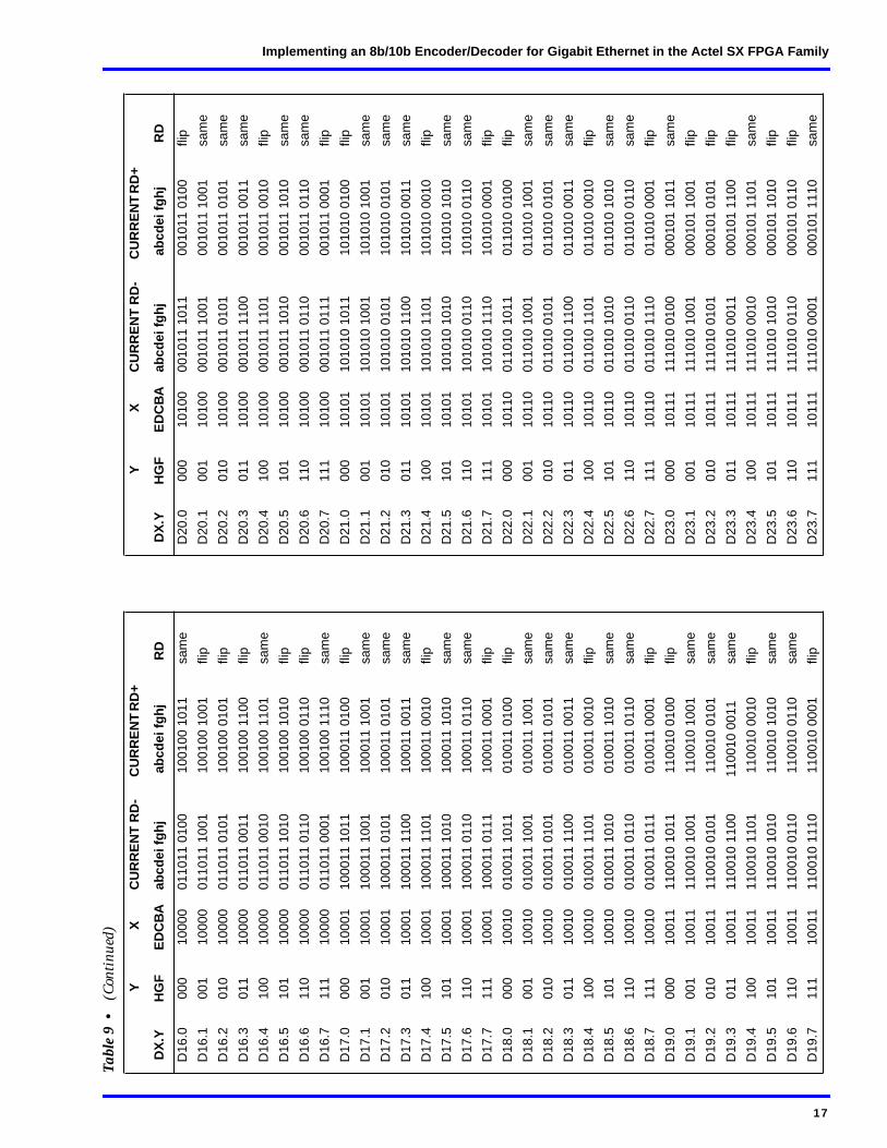
Implementing an 8b/10b Encoder/Decoder for Gigabit Ethernet in the Actel SX FPGA Family
D16
.000
010
000
0110
11 0
100
100
100
1011
sam
eD
20.0
000
1010
000
1011
101
1 0
0101
1 01
00fli
p
D16
.100
110
000
0110
11 1
001
100
100
1001
flip
D20
.100
110
100
0010
11 1
001
001
011
1001
sam
e
D16
.201
010
000
0110
11 0
101
100
100
0101
flip
D20
.201
010
100
0010
11 0
101
001
011
0101
sam
e
D16
.301
110
000
0110
11 0
011
100
100
1100
flip
D20
.301
110
100
0010
11 1
100
001
011
0011
sam
e
D16
.410
010
000
0110
11 0
010
100
100
1101
sam
eD
20.4
100
1010
000
1011
110
1 0
0101
1 00
10fli
p
D16
.510
110
000
0110
11 1
010
100
100
1010
flip
D20
.510
110
100
0010
11 1
010
001
011
1010
sam
e
D16
.611
010
000
0110
11 0
110
100
100
0110
flip
D20
.611
010
100
0010
11 0
110
001
011
0110
sam
e
D16
.711
110
000
0110
11 0
001
100
100
1110
sam
eD
20.7
111
1010
000
1011
011
1 0
0101
1 00
01fli
p
D17
.000
010
001
1000
11 1
011
100
011
0100
flip
D21
.000
010
101
1010
10 1
011
101
010
0100
flip
D17
.100
110
001
1000
11 1
001
100
011
1001
sam
eD
21.1
001
1010
110
1010
100
1 1
0101
0 10
01sa
me
D17
.201
010
001
1000
11 0
101
100
011
0101
sam
eD
21.2
010
1010
110
1010
010
1 1
0101
0 01
01sa
me
D17
.301
110
001
1000
11 1
100
100
011
0011
sam
eD
21.3
011
1010
110
1010
110
0 1
0101
0 00
11sa
me
D17
.410
010
001
1000
11 1
101
100
011
0010
flip
D21
.410
010
101
1010
10 1
101
101
010
0010
flip
D17
.510
110
001
1000
11 1
010
100
011
1010
sam
eD
21.5
101
1010
110
1010
101
0 1
0101
0 10
10sa
me
D17
.611
010
001
1000
11 0
110
100
011
0110
sam
eD
21.6
110
1010
110
1010
011
0 1
0101
0 01
10sa
me
D17
.711
110
001
1000
11 0
111
100
011
0001
flip
D21
.711
110
101
1010
10 1
110
101
010
0001
flip
D18
.000
010
010
0100
11 1
011
010
011
0100
flip
D22
.000
010
110
0110
10 1
011
011
010
0100
flip
D18
.100
110
010
0100
11 1
001
010
011
1001
sam
eD
22.1
001
1011
001
1010
100
1 0
1101
0 10
01sa
me
D18
.201
010
010
0100
11 0
101
010
011
0101
sam
eD
22.2
010
1011
001
1010
010
1 0
1101
0 01
01sa
me
D18
.301
110
010
0100
11 1
100
010
011
0011
sam
eD
22.3
011
1011
001
1010
110
0 0
1101
0 00
11sa
me
D18
.410
010
010
0100
11 1
101
010
011
0010
flip
D22
.410
010
110
0110
10 1
101
011
010
0010
flip
D18
.510
110
010
0100
11 1
010
010
011
1010
sam
eD
22.5
101
1011
001
1010
101
0 0
1101
0 10
10sa
me
D18
.611
010
010
0100
11 0
110
010
011
0110
sam
eD
22.6
110
1011
001
1010
011
0 0
1101
0 01
10sa
me
D18
.711
110
010
0100
11 0
111
010
011
0001
flip
D22
.711
110
110
0110
10 1
110
011
010
0001
flip
D19
.000
010
011
1100
10 1
011
110
010
0100
flip
D23
.000
010
111
1110
10 0
100
000
101
1011
sam
e
D19
.100
110
011
1100
10 1
001
110
010
1001
sam
eD
23.1
001
1011
111
1010
100
1 0
0010
1 10
01fli
p
D19
.201
010
011
1100
10 0
101
110
010
0101
sam
eD
23.2
010
1011
111
1010
010
1 0
0010
1 01
01fli
p
D19
.301
110
011
1100
10 1
100
1100
10 0
011
sam
eD
23.3
011
1011
111
1010
001
1 0
0010
1 11
00fli
p
D19
.410
010
011
1100
10 1
101
110
010
0010
flip
D23
.410
010
111
1110
10 0
010
000
101
1101
sam
e
D19
.510
110
011
1100
10 1
010
110
010
1010
sam
eD
23.5
101
1011
111
1010
101
0 0
0010
1 10
10fli
p
D19
.611
010
011
1100
10 0
110
110
010
0110
sam
eD
23.6
110
1011
111
1010
011
0 0
0010
1 01
10fli
p
D19
.711
110
011
1100
10 1
110
110
010
0001
flip
D23
.711
110
111
1110
10 0
001
000
101
1110
sam
e
Tabl
e 9
• (
Cont
inue
d)
Y
X
CU
RR
EN
T R
D-
CU
RR
EN
T R
D+
Y
X
CU
RR
EN
T R
D-
CU
RR
EN
T R
D+
DX
.YH
GF
ED
CB
Aab
cdei
fghj
abc
dei f
ghj
RD
D
X.Y
HG
FE
DC
BA
abcd
ei fg
hj a
bcde
i fgh
j R
D
17
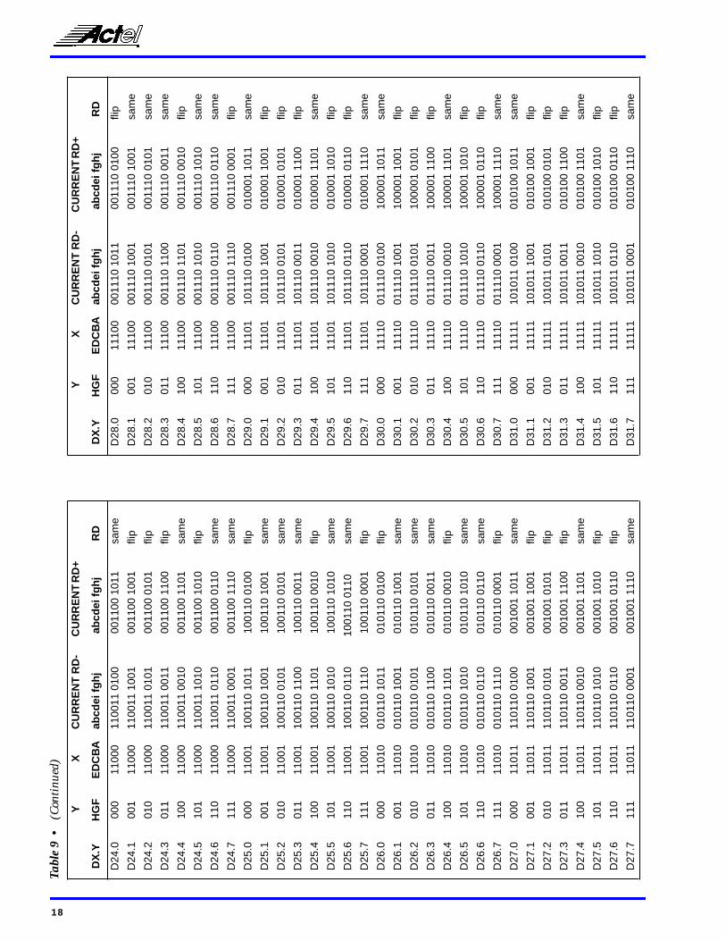
D24
.000
011
000
1100
11 0
100
001
100
1011
sam
eD
28.0
000
1110
000
1110
101
1 0
0111
0 01
00fli
p
D24
.100
111
000
1100
11 1
001
001
100
1001
flip
D28
.100
111
100
0011
10 1
001
001
110
1001
sam
e
D24
.201
011
000
1100
11 0
101
001
100
0101
flip
D28
.201
011
100
0011
10 0
101
001
110
0101
sam
e
D24
.301
111
000
1100
11 0
011
001
100
1100
flip
D28
.301
111
100
0011
10 1
100
001
110
0011
sam
e
D24
.410
011
000
1100
11 0
010
001
100
1101
sam
eD
28.4
100
1110
000
1110
110
1 0
0111
0 00
10fli
p
D24
.510
111
000
1100
11 1
010
001
100
1010
flip
D28
.510
111
100
0011
10 1
010
001
110
1010
sam
e
D24
.611
011
000
1100
11 0
110
001
100
0110
sam
eD
28.6
110
1110
000
1110
011
0 0
0111
0 01
10sa
me
D24
.711
111
000
1100
11 0
001
001
100
1110
sam
eD
28.7
111
1110
000
1110
111
0 0
0111
0 00
01fli
p
D25
.000
011
001
1001
10 1
011
100
110
0100
flip
D29
.000
011
101
1011
10 0
100
010
001
1011
sam
e
D25
.100
111
001
1001
10 1
001
100
110
1001
sam
eD
29.1
001
1110
110
1110
100
1 0
1000
1 10
01fli
p
D25
.201
011
001
1001
10 0
101
100
110
0101
sam
eD
29.2
010
1110
110
1110
010
1 0
1000
1 01
01fli
p
D25
.301
111
001
1001
10 1
100
100
110
0011
sam
eD
29.3
011
1110
110
1110
001
1 0
1000
1 11
00fli
p
D25
.410
011
001
1001
10 1
101
100
110
0010
flip
D29
.410
011
101
1011
10 0
010
010
001
1101
sam
e
D25
.510
111
001
1001
10 1
010
100
110
1010
sam
eD
29.5
101
1110
110
1110
101
0 0
1000
1 10
10fli
p
D25
.611
011
001
1001
10 0
110
1001
10 0
110
sam
eD
29.6
110
1110
110
1110
011
0 0
1000
1 01
10fli
p
D25
.711
111
001
1001
10 1
110
100
110
0001
flip
D29
.711
111
101
1011
10 0
001
010
001
1110
sam
e
D26
.000
011
010
0101
10 1
011
010
110
0100
flip
D30
.000
011
110
0111
10 0
100
100
001
1011
sam
e
D26
.100
111
010
0101
10 1
001
010
110
1001
sam
eD
30.1
001
1111
001
1110
100
1 1
0000
1 10
01fli
p
D26
.201
011
010
0101
10 0
101
010
110
0101
sam
eD
30.2
010
1111
001
1110
010
1 1
0000
1 01
01fli
p
D26
.301
111
010
0101
10 1
100
010
110
0011
sam
eD
30.3
011
1111
001
1110
001
1 1
0000
1 11
00fli
p
D26
.410
011
010
0101
10 1
101
010
110
0010
flip
D30
.410
011
110
0111
10 0
010
100
001
1101
sam
e
D26
.510
111
010
0101
10 1
010
010
110
1010
sam
eD
30.5
101
1111
001
1110
101
0 1
0000
1 10
10fli
p
D26
.611
011
010
0101
10 0
110
010
110
0110
sam
eD
30.6
110
1111
001
1110
011
0 1
0000
1 01
10fli
p
D26
.711
111
010
0101
10 1
110
010
110
0001
flip
D30
.711
111
110
0111
10 0
001
100
001
1110
sam
e
D27
.000
011
011
1101
10 0
100
001
001
1011
sam
eD
31.0
000
1111
110
1011
010
0 0
1010
0 10
11sa
me
D27
.100
111
011
1101
10 1
001
001
001
1001
flip
D31
.100
111
111
1010
11 1
001
010
100
1001
flip
D27
.201
011
011
1101
10 0
101
001
001
0101
flip
D31
.201
011
111
1010
11 0
101
010
100
0101
flip
D27
.301
111
011
1101
10 0
011
001
001
1100
flip
D31
.301
111
111
1010
11 0
011
010
100
1100
flip
D27
.410
011
011
1101
10 0
010
001
001
1101
sam
eD
31.4
100
1111
110
1011
001
0 0
1010
0 11
01sa
me
D27
.510
111
011
1101
10 1
010
001
001
1010
flip
D31
.510
111
111
1010
11 1
010
010
100
1010
flip
D27
.611
011
011
1101
10 0
110
001
001
0110
flip
D31
.611
011
111
1010
11 0
110
010
100
0110
flip
D27
.711
111
011
1101
10 0
001
001
001
1110
sam
eD
31.7
111
1111
110
1011
000
1 0
1010
0 11
10sa
me
Tabl
e 9
• (
Cont
inue
d)
Y
X
CU
RR
EN
T R
D-
CU
RR
EN
T R
D+
Y
X
CU
RR
EN
T R
D-
CU
RR
EN
T R
D+
DX
.YH
GF
ED
CB
Aab
cdei
fghj
abc
dei f
ghj
RD
D
X.Y
HG
FE
DC
BA
abcd
ei fg
hj a
bcde
i fgh
j R
D
18

Implementing an 8b/10b Encoder/Decoder for Gigabit Ethernet in the Actel SX FPGA Family
19

Actel and the Actel logo are registered trademarks of Actel Corporation.
All other trademarks are the property of their owners.
http://www.actel.com
Actel Europe Ltd.Daneshill House, Lutyens CloseBasingstoke, Hampshire RG24 8AGUnited KingdomTel: +44.(0)1256.305600Fax: +44.(0)1256.355420
Actel Corporation955 East Arques AvenueSunnyvale, California 94086USATel: 408.739.1010Fax: 408.739.1540
Actel JapanEXOS Ebisu Bldg. 4F1-24-14 Ebisu Shibuya-kaTokyo 150 JapanTel: +81.(0)3.3445.7671Fax: +81.(0)3.3445.7668
5192650-0/10.98


![2021 -enl* [One Team] oo 3 14:30 FM 82.8MHz 8B 10B 21 a](https://img.pdfslide.us/doc/110x75/617f980d817ba9242432a599/2021-enl-one-team-oo-3-1430-fm-828mhz-8b-10b-21-a-.jpg)