Embed Size (px)
DESCRIPTION
In this paper we have implemented a linear voltage low drop out regulator for efficient power management considering the fact in mind that voltage regulators provide a constant voltage supply to the circuits. We replace the common drain by common source pass element to improve efficiency and reduce the voltage drop across the device. This research paper includes the process to remove the external capacitor allowing for greater power system (soc) application. A compensation scheme is presented that provides both a fast transient response and full range alternating current (ac) stability from 0 to 50 mA load current even if the output load is as high as 100 pf. A 2.7-v capacitorless LDO voltage regulator with a power supply 3 v was designed with a dropout voltage of 300 mv.
Citation preview
INTERNATIONAL JOURNAL OF TECHNOLOGICAL EXPLORATION AND LEARNING (IJTEL)
www.ijtel.org
IJTEL, ISSN: 2319-2135, VOL.3, NO.3, JUNE 2014 460
Implementation of a Capacitor Less Low Dropout
Voltage Regulator on Chip (SOC)
Shailika Sharma
M.TECH-Advance Electronics and Communication
JSS Academy of Technical Education
New Delhi, India
Himani Mittal
Department of E&C
A.P-J.S.S Academy of Technical Education
Noida, India
Abstract— In this paper we have implemented a linear voltage
low drop out regulator for efficient power management
considering the fact in mind that voltage regulators provide a
constant voltage supply to the circuits. We replace the common
drain by common source pass element to improve efficiency and
reduce the voltage drop across the device. This research paper
includes the process to remove the external capacitor allowing for
greater power system (soc) application. A compensation scheme
is presented that provides both a fast transient response and full
range alternating current (ac) stability from 0 to 50 mA load
current even if the output load is as high as 100 pf. A 2.7-v
capacitorless LDO voltage regulator with a power supply 3 v was designed with a dropout voltage of 300 mv.
Keywords-Capacitor less voltage Regulator; Compensated
Transient Response; Power Management Solutions; AC stability.
I. INTRODUCTION
Low dropout regulators have gained importance due to demand for power efficient circuits in mobile communication applications, which require increased battery life. The study of power management techniques has increased spectacularly within the last few years corresponding to a vast increase in the use of portable, handheld battery operated devices. A power management system contains several subsystems including linear regulators, switching regulators, and control logic. The control logic changes the attributes of each subsystem, turning the outputs on and off as well as changing the output voltage levels, to optimize the power consumption of the device.
This paper focuses on low-dropout (LDO) voltage
regulators. LDO regulators are important part of the power
management system which provides constant voltage supply
rails. They come under the class of linear voltage regulators
with improved power efficiency. Here common drain is
replaced by a common source pass element to improve
efficiency over linear regulators and reduce the voltage drop across the control device. Smaller voltage headroom in the
pass element results in less power dissipation, making LDO
regulators more suitable for low-voltage, on-chip, power
management solutions.
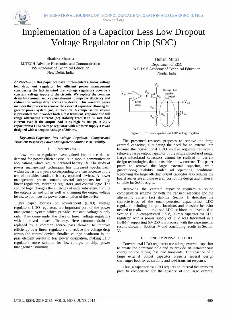
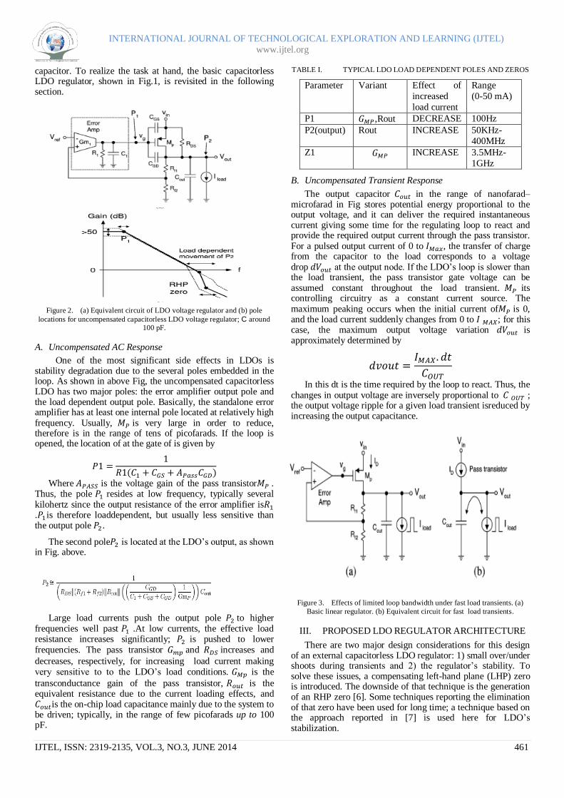
Figure 1. External capacitorless LDO voltage regulator
The presented research proposes to remove the large external capacitor, eliminating the need for an external pin because the conventional LDO voltage regulator requires a relatively large output capacitor in the single microfarad range. Large microfarad capacitors cannot be realized in current design technologies, due to unstable at low currents. This paper poses to remove the large external capacitor, while guaranteeing stability under all operating conditions. Removing the large off-chip output capacitor also reduces the board real estate and the overall cost of the design and makes it suitable for SoC designs.
Removing the external capacitor requires a sound compensation scheme for both the transient response and the alternating current (ac) stability. Section II describes the characteristics of the uncompensated capacitorless LDO regulator including the pole locations and transient behavior needed to realize the proposed LDO architecture developed in Section III. A compensated 2.7-V, 50-mA capacitorless LDO regulator with a power supply of 3 V was fabricated in a BSIM-4 supporting 60- 250 nm process with the experimental results shown in Section IV and concluding results in Section V.
II. UNCOMPENSATED LDO
Conventional LDO regulators use a large external capacitor to create the dominant pole and to provide an instantaneous charge source during fast load transients. The absence of a large external output capacitor presents several design challenges both for ac stability and load transient response.
Thus, a capacitorless LDO requires an internal fast transient path to compensate for the absence of the large external
INTERNATIONAL JOURNAL OF TECHNOLOGICAL EXPLORATION AND LEARNING (IJTEL)
www.ijtel.org
IJTEL, ISSN: 2319-2135, VOL.3, NO.3, JUNE 2014 461
capacitor. To realize the task at hand, the basic capacitorless LDO regulator, shown in Fig.1, is revisited in the following section.
Figure 2. (a) Equivalent circuit of LDO voltage regulator and (b) pole
locations for uncompensated capacitorless LDO voltage regulator; C around 100 pF.
A. Uncompensated AC Response
One of the most significant side effects in LDOs is stability degradation due to the several poles embedded in the loop. As shown in above Fig, the uncompensated capacitorless LDO has two major poles: the error amplifier output pole and the load dependent output pole. Basically, the standalone error amplifier has at least one internal pole located at relatively high frequency. Usually, is very large in order to reduce, therefore is in the range of tens of picofarads. If the loop is opened, the location of at the gate of is given by
Where is the voltage gain of the pass transistor . Thus, the pole resides at low frequency, typically several kilohertz since the output resistance of the error amplifier is . is therefore loaddependent, but usually less sensitive than the output pole .
The second pole is located at the LDO’s output, as shown in Fig. above.
Large load currents push the output pole to higher frequencies well past .At low currents, the effective load resistance increases significantly; is pushed to lower frequencies. The pass transistor and increases and
decreases, respectively, for increasing load current making very sensitive to to the LDO’s load conditions. is the
transconductance gain of the pass transistor, is the equivalent resistance due to the current loading effects, and is the on-chip load capacitance mainly due to the system to be driven; typically, in the range of few picofarads up to 100 pF.
TABLE I. TYPICAL LDO LOAD DEPENDENT POLES AND ZEROS
Parameter Variant Effect of
increased
load current
Range
(0-50 mA)
P1 ,Rout DECREASE 100Hz
P2(output) Rout INCREASE 50KHz-
400MHz
Z1 INCREASE 3.5MHz-
1GHz
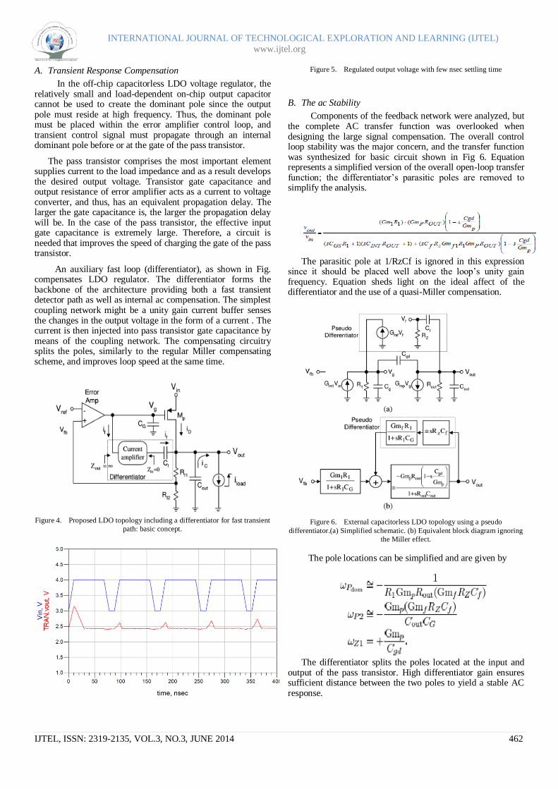
B. Uncompensated Transient Response
The output capacitor in the range of nanofarad–microfarad in Fig stores potential energy proportional to the output voltage, and it can deliver the required instantaneous current giving some time for the regulating loop to react and provide the required output current through the pass transistor. For a pulsed output current of 0 to , the transfer of charge from the capacitor to the load corresponds to a voltage drop at the output node. If the LDO’s loop is slower than the load transient, the pass transistor gate voltage can be assumed constant throughout the load transient. its controlling circuitry as a constant current source. The maximum peaking occurs when the initial current of is 0, and the load current suddenly changes from 0 to ; for this case, the maximum output voltage variation is approximately determined by
In this dt is the time required by the loop to react. Thus, the changes in output voltage are inversely proportional to ; the output voltage ripple for a given load transient isreduced by increasing the output capacitance.
Figure 3. Effects of limited loop bandwidth under fast load transients. (a)
Basic linear regulator. (b) Equivalent circuit for fast load transients.
III. PROPOSED LDO REGULATOR ARCHITECTURE
There are two major design considerations for this design of an external capacitorless LDO regulator: 1) small over/under shoots during transients and 2) the regulator’s stability. To solve these issues, a compensating left-hand plane (LHP) zero is introduced. The downside of that technique is the generation of an RHP zero [6]. Some techniques reporting the elimination of that zero have been used for long time; a technique based on the approach reported in [7] is used here for LDO’s stabilization.
INTERNATIONAL JOURNAL OF TECHNOLOGICAL EXPLORATION AND LEARNING (IJTEL)
www.ijtel.org
IJTEL, ISSN: 2319-2135, VOL.3, NO.3, JUNE 2014 462
A. Transient Response Compensation
In the off-chip capacitorless LDO voltage regulator, the relatively small and load-dependent on-chip output capacitor cannot be used to create the dominant pole since the output pole must reside at high frequency. Thus, the dominant pole must be placed within the error amplifier control loop, and transient control signal must propagate through an internal dominant pole before or at the gate of the pass transistor.
The pass transistor comprises the most important element supplies current to the load impedance and as a result develops the desired output voltage. Transistor gate capacitance and output resistance of error amplifier acts as a current to voltage converter, and thus, has an equivalent propagation delay. The larger the gate capacitance is, the larger the propagation delay will be. In the case of the pass transistor, the effective input gate capacitance is extremely large. Therefore, a circuit is needed that improves the speed of charging the gate of the pass transistor.
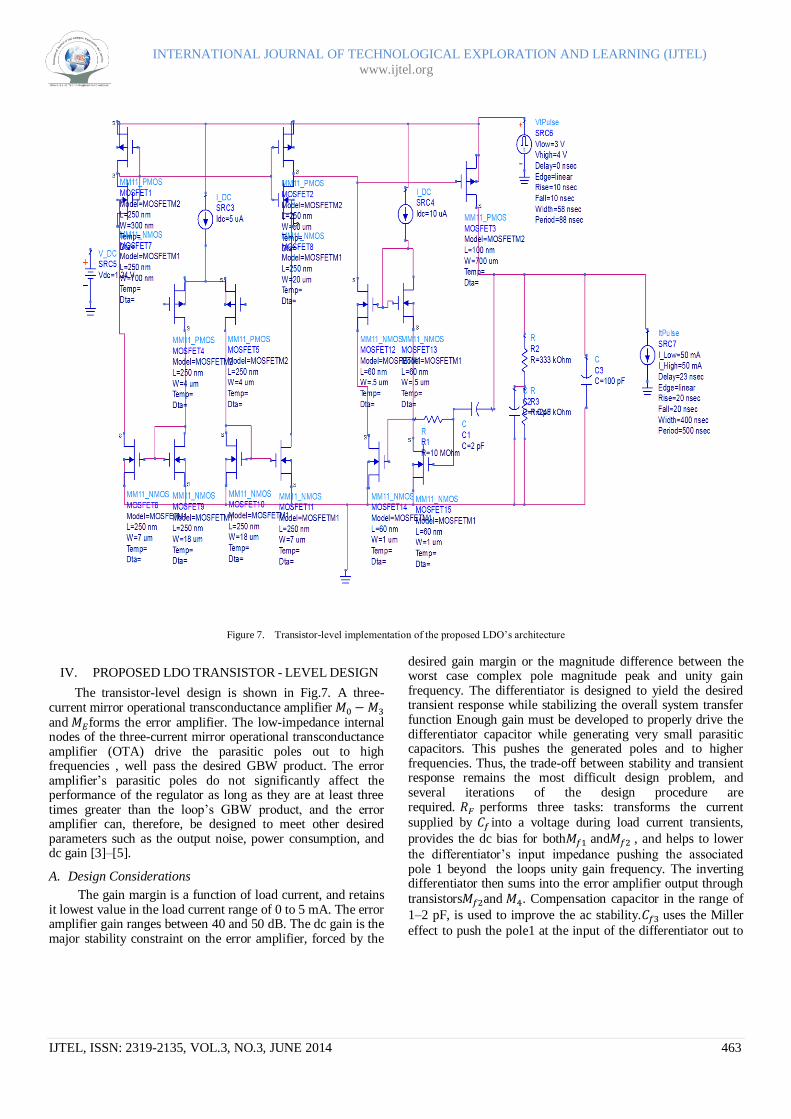
An auxiliary fast loop (differentiator), as shown in Fig. compensates LDO regulator. The differentiator forms the backbone of the architecture providing both a fast transient detector path as well as internal ac compensation. The simplest coupling network might be a unity gain current buffer senses the changes in the output voltage in the form of a current . The current is then injected into pass transistor gate capacitance by means of the coupling network. The compensating circuitry splits the poles, similarly to the regular Miller compensating scheme, and improves loop speed at the same time.
Figure 4. Proposed LDO topology including a differentiator for fast transient
path: basic concept.
Figure 5. Regulated output voltage with few nsec settling time
B. The ac Stability
Components of the feedback network were analyzed, but the complete AC transfer function was overlooked when designing the large signal compensation. The overall control loop stability was the major concern, and the transfer function was synthesized for basic circuit shown in Fig 6. Equation represents a simplified version of the overall open-loop transfer function; the differentiator’s parasitic poles are removed to simplify the analysis.
The parasitic pole at 1/RzCf is ignored in this expression
since it should be placed well above the loop’s unity gain frequency. Equation sheds light on the ideal affect of the differentiator and the use of a quasi-Miller compensation.
Figure 6. External capacitorless LDO topology using a pseudo
differentiator.(a) Simplified schematic. (b) Equivalent block diagram ignoring
the Miller effect.
The pole locations can be simplified and are given by
The differentiator splits the poles located at the input and
output of the pass transistor. High differentiator gain ensures sufficient distance between the two poles to yield a stable AC response.
INTERNATIONAL JOURNAL OF TECHNOLOGICAL EXPLORATION AND LEARNING (IJTEL)
www.ijtel.org
IJTEL, ISSN: 2319-2135, VOL.3, NO.3, JUNE 2014 463
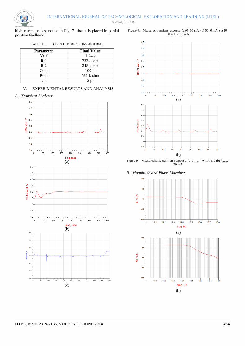
Figure 7. Transistor-level implementation of the proposed LDO’s architecture
IV. PROPOSED LDO TRANSISTOR - LEVEL DESIGN
The transistor-level design is shown in Fig.7. A three-current mirror operational transconductance amplifier and forms the error amplifier. The low-impedance internal nodes of the three-current mirror operational transconductance amplifier (OTA) drive the parasitic poles out to high frequencies , well pass the desired GBW product. The error amplifier’s parasitic poles do not significantly affect the performance of the regulator as long as they are at least three times greater than the loop’s GBW product, and the error amplifier can, therefore, be designed to meet other desired parameters such as the output noise, power consumption, and dc gain [3]–[5].
A. Design Considerations
The gain margin is a function of load current, and retains it lowest value in the load current range of 0 to 5 mA. The error amplifier gain ranges between 40 and 50 dB. The dc gain is the major stability constraint on the error amplifier, forced by the
desired gain margin or the magnitude difference between the worst case complex pole magnitude peak and unity gain frequency. The differentiator is designed to yield the desired transient response while stabilizing the overall system transfer function Enough gain must be developed to properly drive the differentiator capacitor while generating very small parasitic capacitors. This pushes the generated poles and to higher frequencies. Thus, the trade-off between stability and transient response remains the most difficult design problem, and several iterations of the design procedure are required. performs three tasks: transforms the current
supplied by into a voltage during load current transients,
provides the dc bias for both and , and helps to lower
the differentiator’s input impedance pushing the associated pole 1 beyond the loops unity gain frequency. The inverting differentiator then sums into the error amplifier output through
transistors and . Compensation capacitor in the range of
1–2 pF, is used to improve the ac stability. uses the Miller
effect to push the pole1 at the input of the differentiator out to
INTERNATIONAL JOURNAL OF TECHNOLOGICAL EXPLORATION AND LEARNING (IJTEL)
www.ijtel.org
IJTEL, ISSN: 2319-2135, VOL.3, NO.3, JUNE 2014 464
higher frequencies; notice in Fig. 7 that it is placed in partial positive feedback.
TABLE II. CIRCUIT DIMENSIONS AND BIAS
Parameter Final Value
Vref 1.24 v
Rf1 333k ohm
Rf2 248 kohm
Cout 100 pf
Rout 581 k ohm
Cf 2 pf
V. EXPERIMENTAL RESULTS AND ANALYSIS
A. Transient Analysis:
(a)
(b)
(c)
Figure 8. Measured transient response: (a) 0–50 mA, (b) 50–0 mA, (c) 10–
50 mA to 10 mA.
(a)
(b)
Figure 9. Measured Line transient response: (a) = 0 mA and (b) = 50 mA.
B. Magnitude and Phase Margins:
(a)
(b)
INTERNATIONAL JOURNAL OF TECHNOLOGICAL EXPLORATION AND LEARNING (IJTEL)
www.ijtel.org
IJTEL, ISSN: 2319-2135, VOL.3, NO.3, JUNE 2014 465
(c)
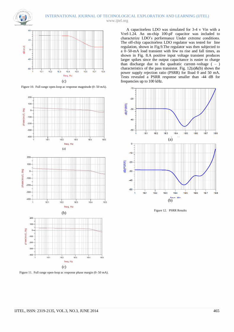
Figure 10. Full range open-loop ac response magnitude (0–50 mA).
(a)
(b)
(c)
Figure 11. Full range open-loop ac response phase margin (0–50 mA).
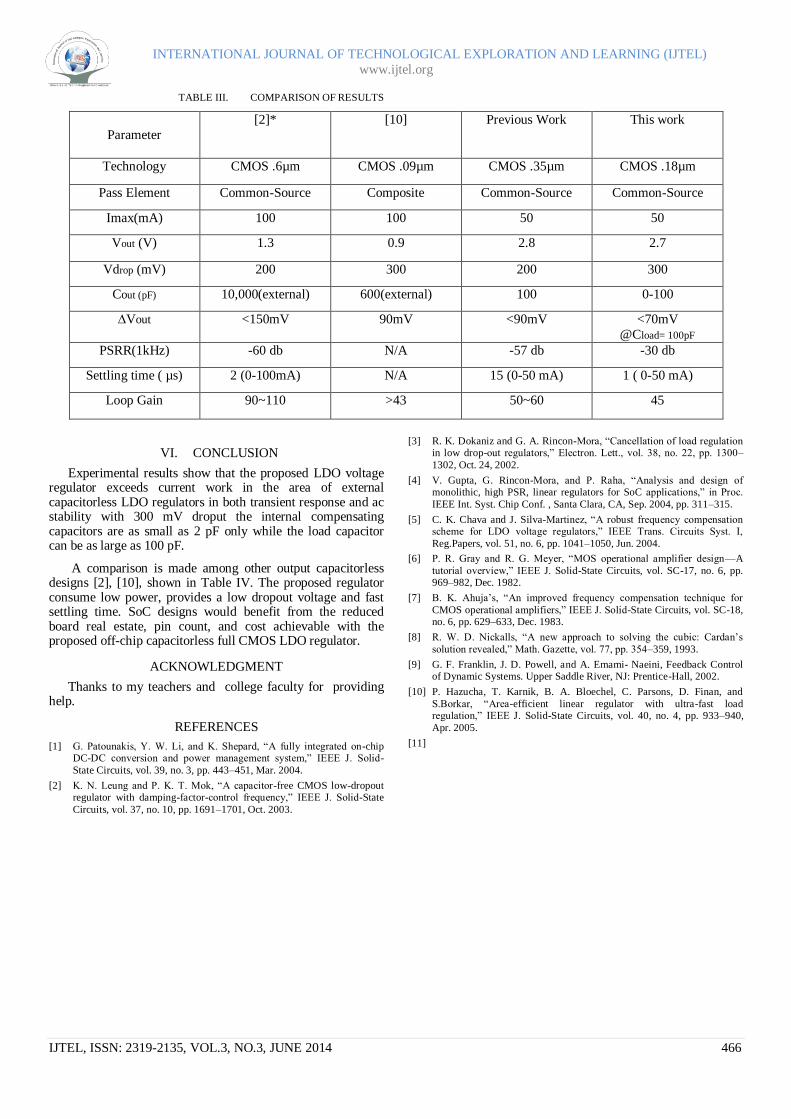
A capacitorless LDO was simulated for 3-4 v Vin with a Vref-1.24. An on-chip 100-pF capacitor was included to characterize LDO’s performance Under extreme conditions. The off-chip capacitorless LDO regulator was tested for line regulation, shown in Fig.9.The regulator was then subjected to a 0–50-mA load transient with few ns rise and fall times, as shown in Fig. 8.A positive input voltage transient produces larger spikes since the output capacitance is easier to charge than discharge due to the quadratic current–voltage ( – ) characteristics of the pass transistor. Fig. 12(a)&(b) shows the power supply rejection ratio (PSRR) for Iload 0 and 50 mA. Tests revealed a PSRR response smaller than -44 dB for frequencies up to 100 kHz.
(a)
(b)
Figure 12. PSRR Results
INTERNATIONAL JOURNAL OF TECHNOLOGICAL EXPLORATION AND LEARNING (IJTEL)
www.ijtel.org
IJTEL, ISSN: 2319-2135, VOL.3, NO.3, JUNE 2014 466
TABLE III. COMPARISON OF RESULTS
Parameter
[2]* [10] Previous Work This work
Technology CMOS .6µm CMOS .09µm CMOS .35µm CMOS .18µm
Pass Element Common-Source Composite Common-Source Common-Source
Imax(mA) 100 100 50 50
Vout (V) 1.3 0.9 2.8 2.7
Vdrop (mV) 200 300 200 300
Cout (pF) 10,000(external) 600(external) 100 0-100
∆Vout <150mV 90mV <90mV <70mV
@Cload= 100pF
PSRR(1kHz) -60 db N/A -57 db -30 db
Settling time ( µs) 2 (0-100mA) N/A 15 (0-50 mA) 1 ( 0-50 mA)
Loop Gain 90~110 >43 50~60 45
VI. CONCLUSION
Experimental results show that the proposed LDO voltage regulator exceeds current work in the area of external capacitorless LDO regulators in both transient response and ac stability with 300 mV droput the internal compensating capacitors are as small as 2 pF only while the load capacitor can be as large as 100 pF.
A comparison is made among other output capacitorless designs [2], [10], shown in Table IV. The proposed regulator consume low power, provides a low dropout voltage and fast settling time. SoC designs would benefit from the reduced board real estate, pin count, and cost achievable with the proposed off-chip capacitorless full CMOS LDO regulator.
ACKNOWLEDGMENT
Thanks to my teachers and college faculty for providing help.
REFERENCES
[1] G. Patounakis, Y. W. Li, and K. Shepard, “A fully integrated on-chip DC-DC conversion and power management system,” IEEE J. Solid-
State Circuits, vol. 39, no. 3, pp. 443–451, Mar. 2004.
[2] K. N. Leung and P. K. T. Mok, “A capacitor-free CMOS low-dropout regulator with damping-factor-control frequency,” IEEE J. Solid-State
Circuits, vol. 37, no. 10, pp. 1691–1701, Oct. 2003.
[3] R. K. Dokaniz and G. A. Rincon-Mora, “Cancellation of load regulation in low drop-out regulators,” Electron. Lett., vol. 38, no. 22, pp. 1300–
1302, Oct. 24, 2002.
[4] V. Gupta, G. Rincon-Mora, and P. Raha, “Analysis and design of monolithic, high PSR, linear regulators for SoC applications,” in Proc.
IEEE Int. Syst. Chip Conf. , Santa Clara, CA, Sep. 2004, pp. 311–315.
[5] C. K. Chava and J. Silva-Martinez, “A robust frequency compensation scheme for LDO voltage regulators,” IEEE Trans. Circuits Syst. I,
Reg.Papers, vol. 51, no. 6, pp. 1041–1050, Jun. 2004.
[6] P. R. Gray and R. G. Meyer, “MOS operational amplifier design—A
tutorial overview,” IEEE J. Solid-State Circuits, vol. SC-17, no. 6, pp. 969–982, Dec. 1982.
[7] B. K. Ahuja’s, “An improved frequency compensation technique for
CMOS operational amplifiers,” IEEE J. Solid-State Circuits, vol. SC-18, no. 6, pp. 629–633, Dec. 1983.
[8] R. W. D. Nickalls, “A new approach to solving the cubic: Cardan’s
solution revealed,” Math. Gazette, vol. 77, pp. 354–359, 1993.
[9] G. F. Franklin, J. D. Powell, and A. Emami- Naeini, Feedback Control of Dynamic Systems. Upper Saddle River, NJ: Prentice-Hall, 2002.
[10] P. Hazucha, T. Karnik, B. A. Bloechel, C. Parsons, D. Finan, and
S.Borkar, “Area-efficient linear regulator with ultra-fast load regulation,” IEEE J. Solid-State Circuits, vol. 40, no. 4, pp. 933–940,
Apr. 2005.
[11]