Embed Size (px)
Citation preview
IA # OIF-CFP2-ACO-01.0 IA for CFP2 Analog Coherent Optics Module
Implementation Agreement for CFP2-Analogue Coherent Optics Module
IA # OIF-CFP2-ACO-01.0
January 22nd 2016
Implementation Agreement created and approved
by the Optical Internetworking Forum www.oiforum.com

IA # OIF-CFP2-ACO-01.0 IA for CFP2 Analog Coherent Optics Module
www.oiforum.com 2
The OIF is an international non-profit organization with over 90 member companies, including the world’s leading carriers and vendors. Being an industry group uniting representatives of the data and optical worlds, OIF’s purpose is to accelerate the deployment of interoperable, cost-effective and robust optical internetworks and their associated technologies. Optical internetworks are data networks composed of routers and data switches interconnected by optical networking elements.
With the goal of promoting worldwide compatibility of optical internetworking products, the OIF actively supports and extends the work of national and international standards bodies. Working relationships or formal liaisons have been established with IEEE 802.1, IEEE 802.3ba, IETF, IP-MPLS Forum, IPv6 Forum, ITU-T SG13, ITU-T SG15, MEF, ATIS-OPTXS, ATIS-TMOC, TMF and the XFP MSA Group.
For additional information contact: The Optical Internetworking Forum, 48377 Fremont Blvd.,
Suite 117, Fremont, CA 94538
510-492-4040, [email protected]
www.oiforum.com
IA # OIF-CFP2-ACO-01.0 IA for CFP2 Analog Coherent Optics Module
www.oiforum.com 3
Working Group: Physical and Link Layer (PLL) Working Group
TITLE: Implementation Agreement for a CFP2 Analogue Coherent Optics Module IA OIF-CFP2-ACO-01.0
SOURCE: TECHNICAL EDITOR PLL WORKING GROUP CHAIR
Ian Betty, Ph.D. David R. Stauffer, Ph.D. Ciena Kandou Bus, SA 3500 Carling Ave QI-I Ottawa, ON K2H 8E9, Canada 1015 Lausanne, Switzerland
Phone: +1-613-670-2160 Phone: +1.802.316.0808 Email: [email protected] Email: [email protected]
PLL WORKING GROUP – OPTICAL VICE CHAIR
Karl Gass Qorvo Phone: +1-505-301-1511 Email: [email protected]
ABSTRACT: Implementation Agreement created and approved by the Optical Internetworking
Forum for a CFP2 Analog Coherent Optics Module. The project start was approved at the Q2 Technical Meeting, April 2013 (Albuquerque, USA). OIF2013.130.01 is the original project start document for this project.

IA # OIF-CFP2-ACO-01.0 IA for CFP2 Analog Coherent Optics Module
www.oiforum.com 4
Notice: This Technical Document has been created by the Optical Internetworking Forum (OIF). This document is
offered to the OIF Membership solely as a basis for agreement and is not a binding proposal on the companies listed as resources above. The OIF reserves the rights to at any time to add, amend, or withdraw statements contained herein. Nothing in this document is in any way binding on the OIF or any of its members.
The user's attention is called to the possibility that implementation of the OIF implementation agreement contained herein may require the use of inventions covered by the patent rights held by third parties. By publication of this OIF implementation agreement, the OIF makes no representation or warranty whatsoever, whether expressed or implied, that implementation of the specification will not infringe any third party rights, nor does the OIF make any representation or warranty whatsoever, whether expressed or implied, with respect to any claim that has been or may be asserted by any third party, the validity of any patent rights related to any such claim, or the extent to which a license to use any such rights may or may not be available or the terms hereof.
© 2016 Optical Internetworking Forum
This document and translations of it may be copied and furnished to others, and derivative works that comment on or otherwise explain it or assist in its implementation may be prepared, copied, published and distributed, in whole or in part, without restriction other than the following, (1) the above copyright notice and this paragraph must be included on all such copies and derivative works, and (2) this document itself may not be modified in any way, such as by removing the copyright notice or references to the OIF, except as needed for the purpose of developing OIF Implementation Agreements. By downloading, copying, or using this document in any manner, the user consents to the terms and conditions of this notice. Unless the terms and conditions of this notice are breached by the user, the limited permissions granted above are perpetual and will not be revoked by the OIF or its successors or assigns.
This document and the information contained herein is provided on an “AS IS” basis and THE OIF DISCLAIMS ALL WARRANTIES, EXPRESS OR IMPLIED, INCLUDING BUT NOT LIMITED TO ANY WARRANTY THAT THE USE OF THE INFORMATION HEREIN WILL NOT INFRINGE ANY RIGHTS OR ANY IMPLIED WARRANTIES OF MERCHANTABILITY, TITLE OR FITNESS FOR A PARTICULAR PURPOSE.
IA # OIF-CFP2-ACO-01.0
IA for CFP2 Analog Coherent Optics Module
www.oiforum.com 5
LIST OF FIGURES ............................................................................................... 8
LIST OF TABLES ................................................................................................. 8
1 Document Revision History ........................................................................ 9 2 Reference Documents.............................................................................. 10
2.1 Normative References ........................................................................ 10
3 Introduction .............................................................................................. 11 4 CFP2-ACO Module Functions .................................................................. 12
4.1 Transmit (Tx) Coherent Optics Function Block Diagrams ................... 13 4.2 Receive (Rx) Coherent Optics Function Block Diagrams ................... 15 4.3 Laser Sources (Tx and Rx LO) ........................................................... 17
4.4 Integrated Polarization Multiplexed Quadrature Mach-Zehnder Modulator (PMQ Modulator) ........................................................................ 18 4.5 Intradyne Coherent Receiver (ICR) .................................................... 18
4.6 MZ Modulator RF Drivers ................................................................... 19
4.7 Optical Power Monitoring and Control ................................................ 19 4.8 MDIO Management Interface Specification ........................................ 20 4.9 Electronics .......................................................................................... 20
5 CFP2-ACO Module Classification by Electrical Interface ......................... 20 6 CFP2-ACO Module Mechanicals and Power ........................................... 21
6.1 Overview............................................................................................. 21 6.2 Mechanical Dimensions ...................................................................... 22 6.3 Optical Connector ............................................................................... 22
6.4 Module Power Dissipation Classes .................................................... 23
6.5 Module Bail Latch Color ..................................................................... 23 7 CFP2-ACO Module Thermal Interface Requirements .............................. 24
7.1 Data Requirements ............................................................................. 24
7.2 Thermal Environment ......................................................................... 24 7.3 Thermal Interface Area ....................................................................... 24
7.4 Module Thermal Interface Surface Requirements .............................. 25 7.5 Thermal Sensor Calibration ................................................................ 25
8 CFP2-ACO Electrical Connector Interface ............................................... 25
8.1 104-Pin Electrical Connector .............................................................. 25 8.1.1 Background .................................................................................. 25
8.1.2 Photographs of Connector: Plug and Host ................................... 26
8.1.3 Suppliers and Example Part Numbers ......................................... 26
8.1.4 Reliability and Environmental Test Documentation ...................... 27
8.1.5 Connector Ratings ....................................................................... 27
8.1.6 RF Path S-Parameters ................................................................. 27
8.1.7 Connector Cross Mating .............................................................. 27
8.1.8 Related CFP2 Cage Products ...................................................... 27
8.2 Electrical Pin Maps ............................................................................. 28 8.2.1 Class 1 and Class 2 Electrical Pin Map........................................ 28
IA # OIF-CFP2-ACO-01.0
IA for CFP2 Analog Coherent Optics Module
www.oiforum.com 6
8.2.2 Class 3 Electrical Pin Map with the Full Superset Analog Control Interface (ACI) .......................................................................................... 29
8.3 Allowed Tx and Rx RF Channel Mappings ......................................... 31 9 CFP2-ACO Tx and Rx RF Electrical Interfaces ........................................ 32
9.1 Introduction ......................................................................................... 32 9.2 Tx and Rx Electrical Interface Specification Compliance Points ......... 33 9.3 Compliance Board Suppliers and Example Part Numbers ................. 34 9.4 Compliance Board S Parameter Requirements .................................. 35 9.5 Class 1: RF Electrical Interface Specifications .................................. 36
9.5.1 Class 1: Tx RF Interface Specifications ...................................... 36
9.5.2 Class 1: Rx RF Interface Specifications ....................................... 37
9.6 Class 2/3: RF Electrical Interface Specifications ............................... 38 9.6.1 Class 2/3: Tx RF Interface Specifications ................................... 38
9.6.2 Class 2/3: Rx RF Interface Electrical Specifications ................... 40
10 Class 3 Analogue Control Interface (ACI) Requirements ....................... 43 10.1 Tx MZ Arm Phase Control Dither Inputs .......................................... 44
10.2 Tx X-Pol. and Y-Pol. Power Control Dither Inputs ........................... 45 10.3 Tx Optical Power Monitor Taps ....................................................... 45
10.4 Rx TIA/VGA Gain Control Inputs ..................................................... 46 10.5 PM_SYNC Input .............................................................................. 46 10.6 TX_DIS Input and RX_LOS Output Configurability ......................... 47
11 MDIO Register Interface ........................................................................ 48
11.1 Implementation Overview ................................................................ 48 11.2 CFP2-ACO Calibration Data ........................................................... 49 11.3 CFP2-ACO User Private Use Registers .......................................... 49
12 OIF Requested CFP MSA MIS V2.4 R06b Extensions and Modifications Supporting the CFP2-ACO Module (Informative) ............................................ 50
12.1 OIF Requested Changes to Existing CFP MSA MIS V2.4 R06b Content ........................................................................................................ 50 12.2 New MDIO Registers for Tx Subsystem Control ............................. 52 12.3 New MDIO Registers for Rx Subsystem Control ............................. 61 12.4 CFP2-ACO Fault, Alarm, Warning and Status (FAWS) Registers ... 67
12.5 CFP2-ACO Wavelength Change Operation .................................... 68 12.6 CFP2-ACO Wavelength Selection Registers .................................. 69
12.6.1 Use of the High Resolution Tuning Registers ........................... 70
12.7 CFP2-ACO Module Characteristic Data Registers .......................... 72
13 Relevant 0xB000 MDIO Registers in CFP MSA MIS V2.4 R06b (Informative) .................................................................................................... 76
13.1 Tx and Rx Laser Source Control ..................................................... 76 13.2 Tx and Rx Laser Source Performance Monitoring........................... 78 13.3 Rx Input Power Monitor ................................................................... 79 13.4 Tx Output Power and Monitoring (VOA Control) ............................. 80 13.5 Modulator Bias Voltages ................................................................. 80 13.6 FAWS Registers .............................................................................. 80
IA # OIF-CFP2-ACO-01.0
IA for CFP2 Analog Coherent Optics Module
www.oiforum.com 7
14 Glossary ................................................................................................. 85 15 Annex A: HCB and MCB Differential Insertion Losses ........................... 86 16 Annex B: Mated HCB and MCB S-Parameters ...................................... 87 17 Appendix I: Electrical Connector S-Parameters (Informative) ............... 90 18 Appendix II: Beat Frequency Skew Measurement Method (Informative) 91 19 Open Issues / Current Work Items ......................................................... 91 20 List of Companies Belonging to OIF when Document is Approved ........ 92
IA # OIF-CFP2-ACO-01.0
IA for CFP2 Analog Coherent Optics Module
www.oiforum.com 8
List of Figures
FIGURE 1: CFP2-ACO MODULE ILLUSTRATION1 ......................................................................................................12
FIGURE 2 CFP2-ACO MODULE HIGH LEVEL BLOCK DIAGRAM ....................................................................................13 FIGURE 3: SUPERSET TRANSMIT FUNCTION BLOCK DIAGRAM WITH AN MDIO ONLY CONTROL INTERFACE ..........................14 FIGURE 4: SUPERSET TRANSMIT FUNCTION BLOCK DIAGRAM WITH AN MDIO PLUS FULL SUPERSET ANALOG CONTROL
INTERFACE (ACI) ......................................................................................................................................15 FIGURE 5: SUPERSET RECEIVE FUNCTION BLOCK DIAGRAM WITH AN MDIO ONLY CONTROL INTERFACE .............................16 FIGURE 6: SUPERSET RECEIVE FUNCTION BLOCK DIAGRAM WITH AN MDIO PLUS FULL SUPERSET ANALOG CONTROL INTERFACE
(ACI)......................................................................................................................................................17 FIGURE 7: CFP2-ACO ALLOWED CONNECTOR POSITIONS (CENTERED, LEFT JUSTIFIED, AND RIGHT JUSTIFIED) WITH
DIMENSIONAL TOLERANCES. .......................................................................................................................23 FIGURE 8 : (A) PLUG BOTTOM SIDE SHOWING SEQUENCED CONNECTION CONTACTS, (B) PLUG TOP SIDE SHOWING GSSG
FORMAT RF CONTACT GROUPS, (C) HOST CONNECTOR REAR VIEW – PINS CONNECTED TO HOST PCBS, (D) HOST
CONNECTOR FRONT VIEW – ACCEPTS THE PLUG. .............................................................................................26 FIGURE 9: SINGLE CFP2 CAGE ILLUSTRATION (INFORMATIVE). ....................................................................................28 FIGURE 10 (A) CLASS 1 AND 2 ELECTRICAL PIN MAP, (B) CLASS 3 FULL SUPERSET ACI INTERFACE ELECTRICAL PIN MAP. ......30 FIGURE 11: I AND Q PHASE DEFINITIONS ................................................................................................................32 FIGURE 12: HIGH-SPEED I/O FOR DATA .................................................................................................................32 FIGURE 13: INFORMATIVE RF CHANNEL IMPLEMENTATION EXAMPLE ...........................................................................33 FIGURE 14: TX AND RX ELECTRICAL INTERFACE COMPLIANCE POINTS. THE PROVIDED HCB AND MCB IMPLEMENTATION
PICTURES ARE INFORMATIVE EXAMPLES ONLY. ...............................................................................................34 FIGURE 15: CLASS 1 TX RF INTERFACE DRIVE SIGNAL EYE-MASK @ TP1A ....................................................................37 FIGURE 16: NORMALIZED TX EO MAG(S21) COMPLIANCE MASK ..............................................................................40 FIGURE 17: NORMALIZED RX OE CG MAG(S21) COMPLIANCE MASK ........................................................................42 FIGURE 18: TX ANALOG CONTROL INTERFACE (ACI) SCHEMATIC .................................................................................44 FIGURE 19: RX ANALOG CONTROL INTERFACE (ACI) SCHEMATIC .................................................................................44 FIGURE 20: WAVELENGTH CHANGE SEQUENCE (A) CLASS 1 AND 2, (B) CLASS 3. ...........................................................69 FIGURE 21: ACCESS METHODOLOGY TO OBTAIN CLASS 2 AND CLASS 3 MODULE CHARACTERISTIC DATA ............................75 FIGURE 22: REFERENCE DIFFERENTIAL INSERTION LOSSES FOR THE PCB TRACES ON TWO MODULE COMPLIANCE BOARDS
[MCB SDD21] ........................................................................................................................................86 FIGURE 23: REFERENCE DIFFERENTIAL INSERTION LOSSES FOR THE PCB TRACES ON A HOST COMPLIANCE BOARD [HCB
SDD21] .................................................................................................................................................86 FIGURE 24: MATED HCB-MCB SDD11, SDD22 ....................................................................................................87 FIGURE 25: MATED HCB-MCB SCD21, SCD12.....................................................................................................88 FIGURE 26: MATED HCB-MCB SCD11, SCD22 AND SDC11, SDC22 .......................................................................88 FIGURE 27: MATED HCB-MCB SDD21, SDD12 ....................................................................................................89 FIGURE 28: MATED CFP2 CONNECTOR SI PERFORMANCE MEASUREMENT CONDITIONS .................................................90 FIGURE 29: TYPICAL MATED CFP2 CONNECTOR SI PERFORMANCE..............................................................................91 FIGURE 30: BEAT FREQUENCY SKEW MEASUREMENT METHOD...................................................................................91
List of Tables
TABLE 1: IA DOCUMENT REVISION HISTORY ..............................................................................................................9 TABLE 2: CFP2-ACO MODULE CLASSIFICATION BY ELECTRICAL INTERFACE ...................................................................21 TABLE 3: CFP2-ACO RELEVANT CFP-MSA HARDWARE SPECIFICATION REFERENCES .....................................................22 TABLE 4: CFP2 CONNECTOR SUPPLIERS AND PART NUMBERS .....................................................................................26 TABLE 5: CFP2 CONNECTOR RELIABILITY DOCUMENTS ..............................................................................................27 TABLE 6: CFP2 CONNECTOR RATINGS ....................................................................................................................27 TABLE 7: RELATED CFP2 CAGE PART NUMBERS .......................................................................................................28 TABLE 8: TX AND RX RF CHANNEL MAPPINGS ON THE ELECTRICAL CONNECTOR INTERFACE ..............................................31 TABLE 9: COMPLIANCE BOARD SUPPLIERS AND PART NUMBERS ..................................................................................34
IA # OIF-CFP2-ACO-01.0
IA for CFP2 Analog Coherent Optics Module
www.oiforum.com 9
TABLE 10: CLASS 1 CFP2-ACO MODULE TX RF INTERFACE ELECTRICAL SPECIFICATIONS .................................................36 TABLE 11: CLASS 1 CFP2-ACO MODULE RX RF INTERFACE ELECTRICAL SPECIFICATIONS.................................................37 TABLE 12: CLASS 2/3 CFP2-ACO MODULE TX RF INTERFACE ELECTRICAL SPECIFICATIONS FOR A MODULE CONTROLLED PMQ
TRANSMITTER ..........................................................................................................................................38 TABLE 13: CLASS 3 CFP2-ACO MODULE TX RF INTERFACE ELECTRICAL SPECIFICATIONS FOR A HOST CONTROLLED PMQ
TRANSMITTER ..........................................................................................................................................40 TABLE 14: CLASS 2/3 CFP2-ACO MODULE RX RF INTERFACE ELECTRICAL SPECIFICATIONS .............................................42 TABLE 15 REQUESTED CHANGES TO CFP MSA MIS V2.4 R06B REGISTERS ..................................................................51 TABLE 16: TX SUBSYSTEM MDIO REGISTERS ...........................................................................................................60 TABLE 17: RX SUBSYSTEM MDIO REGISTERS ..........................................................................................................65 TABLE 18: RX SUBSYSTEM MDIO REGISTERS CONTINUED..........................................................................................67 TABLE 19: CFP MSA MIS V2.4 R06B LASER CONTROL REGISTERS .............................................................................69 TABLE 20: TX MINIMUM LASER FREQUENCY REGISTERS ............................................................................................71 TABLE 21: TX TUNED LASER FREQUENCY REGISTERS .................................................................................................71 TABLE 22: RX MINIMUM LASER FREQUENCY REGISTERS ............................................................................................72 TABLE 23: RX TUNED LASER FREQUENCY REGISTERS .................................................................................................72 TABLE 24: MDIO MODULE CHARACTERISTIC DATA REGISTERS ...................................................................................75 TABLE 25: GLOSSARY ..........................................................................................................................................85
Document Revision History 1
Table 1 provides the OIF-CFP2-ACO-1.0 IA document revision history.
Document Date Revisions/Comments
OIF2013.130.01 April 19th
2013 Project Start: CFP2 Coherent Optics Transceiver
Module
OIF-CFP2-ACO-01.0 January
22nd 2016 Release created from OIF2014.006.19
Table 1: IA Document Revision History
IA # OIF-CFP2-ACO-01.0
IA for CFP2 Analog Coherent Optics Module
www.oiforum.com 10
Reference Documents 2
2.1 Normative References
[1] www.cfp-msa.org
[2] CFP MSA Management Interface Specification, Version 2.4 R06b (June 8th 2015)
[3] CFP MSA CFP2 Hardware Specification Revision 1.0, 31 July 2013
[4] CFP MSA CFP/CFP2/CFP4 Pin Allocation Rev. 25
[5] OIF-MSA-100GLH-EM-01.1 - Multisource Agreement for 100G Long-Haul DWDM Transmission Module - Electromechanical (September 2011)
[6] OIF-PMQ-TX-01.2 - Implementation Agreement for Integrated Polarization Multiplexed Quadrature Modulated Transmitters (May 2015)
[7] OIF-DPC-RX-01.2 - Implementation Agreement for Integrated Dual Polarization Intradyne Coherent Receivers (November 2013)
[8] OIF-microITLA-01.1 – Implementation Agreement for Micro Integrable Tunable Laser Assembly (July 2015)
[9] OIF-ITLA-MSA-01.3 - Integrable Tunable Laser Assembly Multi Source Agreement (July 2015)
[10] OIF-CEI-03.1 - Common Electrical I/O (CEI) - Electrical and Jitter Interoperability agreements for 6G+ bps, 11G+ bps, 25G+ bps I/O (February 2014)
[11] CFP2 Hardware Baseline Design Rev. 1L
[12] Implementation Agreement for Thermal Interface Specification for Pluggable Optics Modules (May 2015)
[13] OIF-DPC-MRX-01.0 - Implementation Agreement for Integrated Dual Polarization Micro-Intradyne Coherent Receivers (March 2015)
[14] Telcordia NEBSTM Requirements: Physical Protection, Telcordia Technologies Generic Requirements, GR-63-CORE Issue 3, March 2006.
IA # OIF-CFP2-ACO-01.0
IA for CFP2 Analog Coherent Optics Module
www.oiforum.com 11
Introduction 3
Faceplate density of optical IO is a key metric for switching and line-side transport applications. The industry experience is that this faceplate density is maximized when high power electronics are removed from optical modules [e.g. CFP → CFP2 → CFP4 for 100GbE client modules.]
Faceplate density improvements can be realized for line-side optical transport by placing coherent DSP engines on the Host board and the E-to-O conversion functions within a CFP2 Analog Coherent Optics (CFP2-ACO) module. This architecture for line cards, that broadly separates optical and electronic DSP functions, offers the following additional benefits:
Margin stacking of the coherent DSP engine in the supply chain is removed.
Coherent DSP engine development is decoupled from the electro-optics development, which is beneficial since they have different supply chains and development cadences. This decoupling also enables specialization within the supply chain and reduces duplication of development efforts.
Optimal cooling of the optical and electronic DSP functions is possible, enabling higher performance line-side applications. Shared heat sinking between low temperature optics and high temperature electronics is avoided and there is no inefficient “box”-in-“box” thermal stacking:
o A Host board coherent DSP engine can have a permanently attached full slot height heat sink with excellent thermal interface conductivity. The DSP engine can operate with high junction temperatures.
o A faceplate pluggable module has limited space available for a riding heat sink and the interface thermal conductivity is limited by both the maximum spring force that can be applied to the module and the module surface roughness. A pluggable module is best suited to relatively low power E-to-O conversion functionality.
The dominant coherent modem Bill of Material (BOM) cost along with the main contributors to reliability FITs (Failures in Time) become hot- pluggable within the CFP2-ACO module. This addresses the problem of the modem first-in install cost in multi-port line cards. It also allows the selection of the best-fit CFP2-ACO module for each system application at the time of deployment (price/performance/power/etc.)
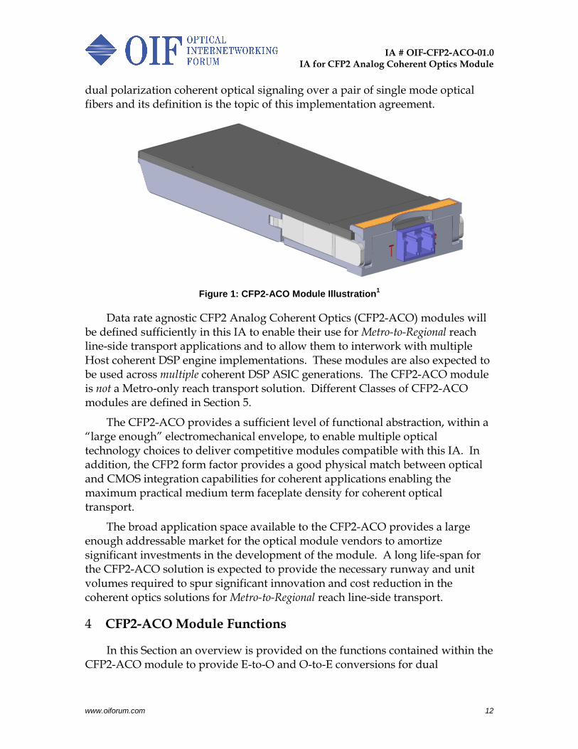
Figure 1 shows a CFP2-ACO module for illustration purposes only1. The CFP2-ACO module contains all the required functions to perform bi-directional
1 Do not use Figure 1 for design detail or scale.
IA # OIF-CFP2-ACO-01.0
IA for CFP2 Analog Coherent Optics Module
www.oiforum.com 12
dual polarization coherent optical signaling over a pair of single mode optical fibers and its definition is the topic of this implementation agreement.
Figure 1: CFP2-ACO Module Illustration1
Data rate agnostic CFP2 Analog Coherent Optics (CFP2-ACO) modules will be defined sufficiently in this IA to enable their use for Metro-to-Regional reach line-side transport applications and to allow them to interwork with multiple Host coherent DSP engine implementations. These modules are also expected to be used across multiple coherent DSP ASIC generations. The CFP2-ACO module is not a Metro-only reach transport solution. Different Classes of CFP2-ACO modules are defined in Section 5.
The CFP2-ACO provides a sufficient level of functional abstraction, within a “large enough” electromechanical envelope, to enable multiple optical technology choices to deliver competitive modules compatible with this IA. In addition, the CFP2 form factor provides a good physical match between optical and CMOS integration capabilities for coherent applications enabling the maximum practical medium term faceplate density for coherent optical transport.
The broad application space available to the CFP2-ACO provides a large enough addressable market for the optical module vendors to amortize significant investments in the development of the module. A long life-span for the CFP2-ACO solution is expected to provide the necessary runway and unit volumes required to spur significant innovation and cost reduction in the coherent optics solutions for Metro-to-Regional reach line-side transport.
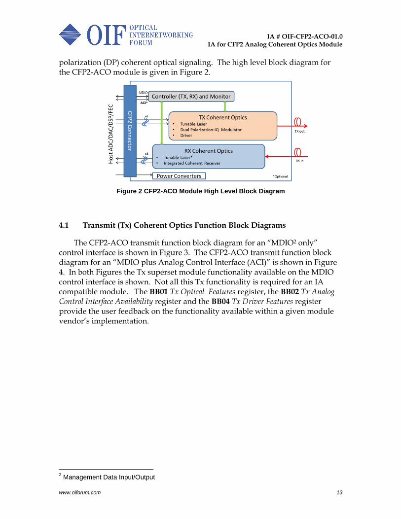
CFP2-ACO Module Functions 4
In this Section an overview is provided on the functions contained within the CFP2-ACO module to provide E-to-O and O-to-E conversions for dual
IA # OIF-CFP2-ACO-01.0
IA for CFP2 Analog Coherent Optics Module
www.oiforum.com 13
polarization (DP) coherent optical signaling. The high level block diagram for the CFP2-ACO module is given in Figure 2.
Figure 2 CFP2-ACO Module High Level Block Diagram
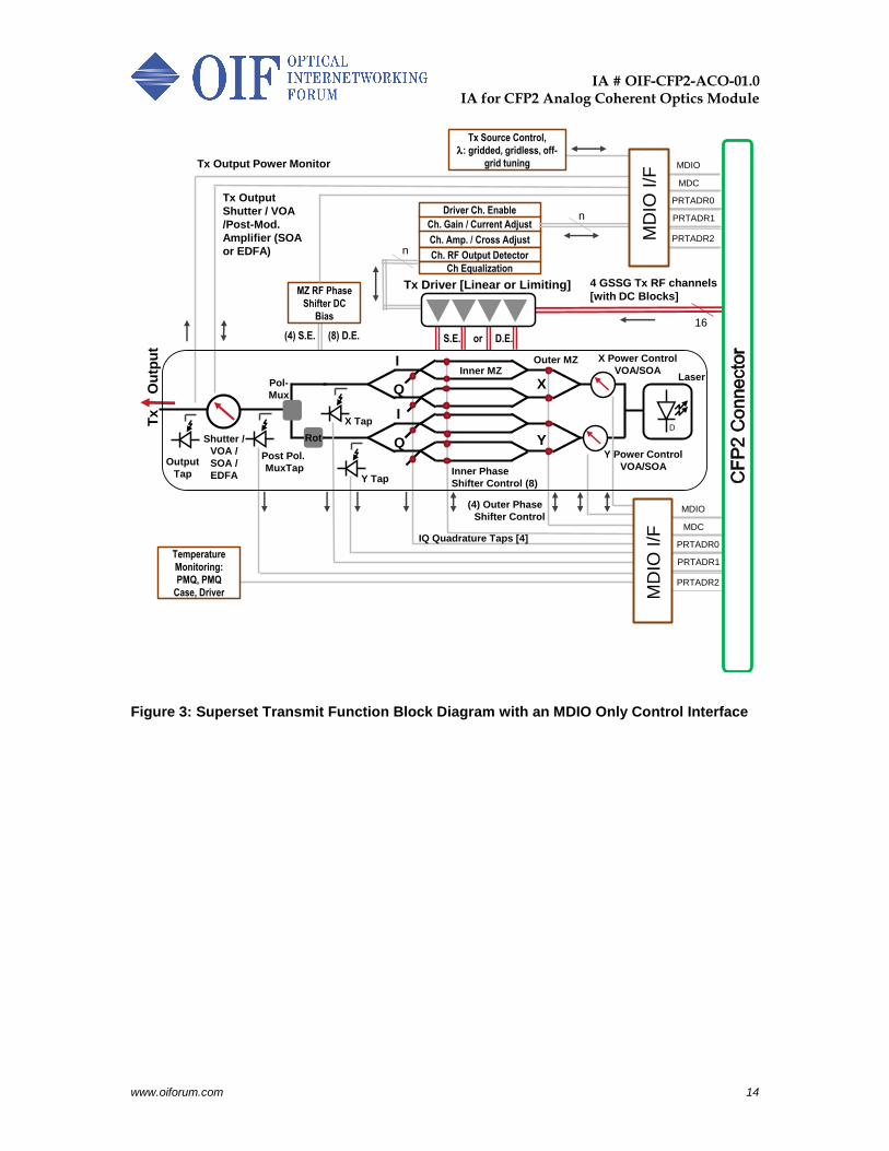
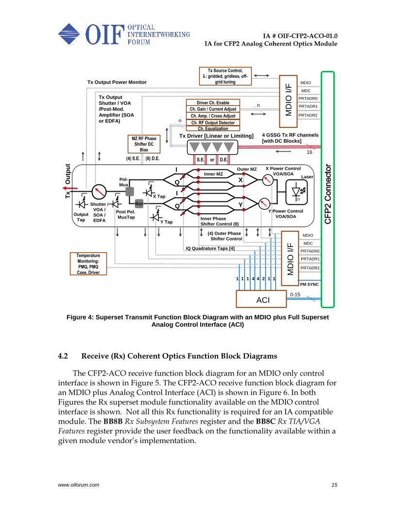
4.1 Transmit (Tx) Coherent Optics Function Block Diagrams
The CFP2-ACO transmit function block diagram for an “MDIO2 only” control interface is shown in Figure 3. The CFP2-ACO transmit function block diagram for an “MDIO plus Analog Control Interface (ACI)” is shown in Figure 4. In both Figures the Tx superset module functionality available on the MDIO control interface is shown. Not all this Tx functionality is required for an IA compatible module. The BB01 Tx Optical Features register, the BB02 Tx Analog Control Interface Availability register and the BB04 Tx Driver Features register provide the user feedback on the functionality available within a given module vendor’s implementation.
2 Management Data Input/Output
ACI*
IA # OIF-CFP2-ACO-01.0
IA for CFP2 Analog Coherent Optics Module
www.oiforum.com 14
Figure 3: Superset Transmit Function Block Diagram with an MDIO Only Control Interface
MDC
MDIO
PRTADR0
PRTADR1
PRTADR2
Ch. Gain / Current Adjust
Ch. Amp. / Cross Adjust
Ch. RF Output Detector
Ch Equalization
n
Tx Output Power Monitor
16
4 GSSG Tx RF channels
[with DC Blocks]Tx Driver [Linear or Limiting]
Driver Ch. Enable
Tx Source Control,
l: gridded, gridless, off-
grid tuning
Tx Output
Shutter / VOA
/Post-Mod.
Amplifier (SOA
or EDFA)
Tx O
utp
ut
n
D
MDC
MDIO
PRTADR0
PRTADR1
PRTADR2
S.E. or D.E.
Output
Tap
Pol-
Mux
Shutter /
VOA /
SOA /
EDFA
Y Power Control
VOA/SOA
X Power Control
VOA/SOA
Rot
MZ RF Phase
Shifter DC
Bias
(4) S.E. (8) D.E.
X
Y
I
Q
I
QPost Pol.
MuxTap
X Tap
Y Tap
MD
IO I
/F
Laser
Outer MZInner MZ
MD
IO I
/FIQ Quadrature Taps [4]
Inner Phase
Shifter Control (8)
(4) Outer Phase
Shifter Control
Temperature
Monitoring:
PMQ, PMQ
Case, Driver
IA # OIF-CFP2-ACO-01.0
IA for CFP2 Analog Coherent Optics Module
www.oiforum.com 15
Figure 4: Superset Transmit Function Block Diagram with an MDIO plus Full Superset Analog Control Interface (ACI)
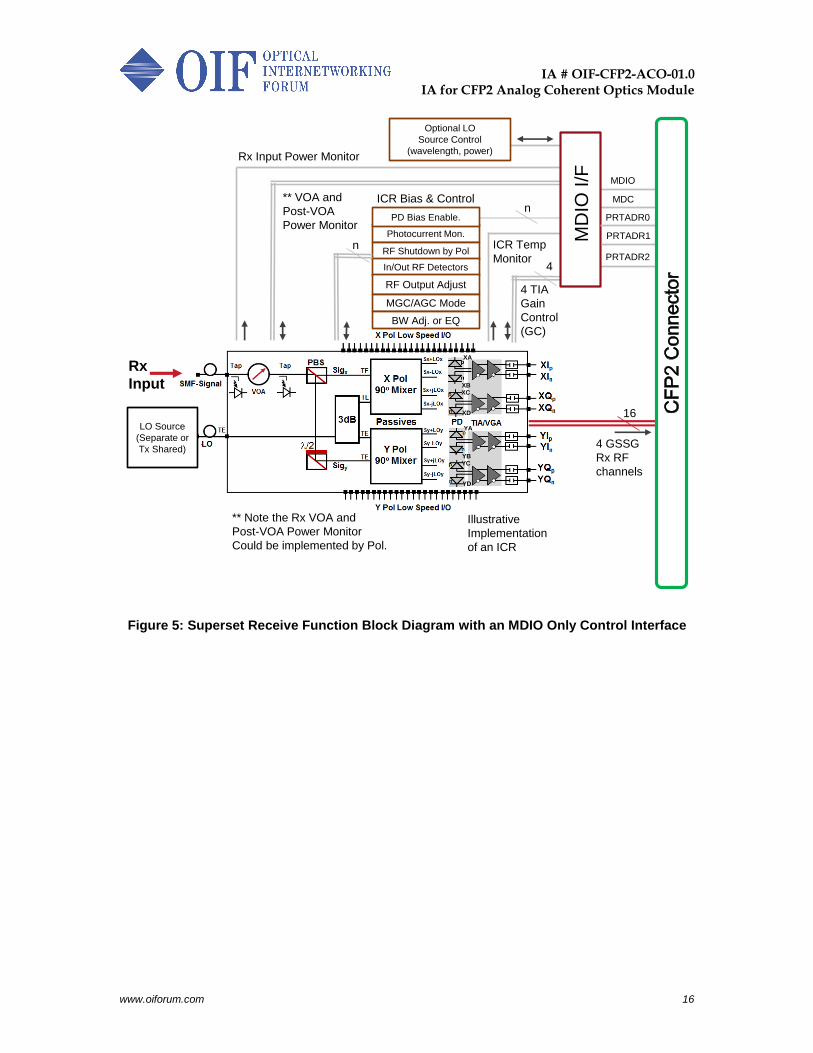
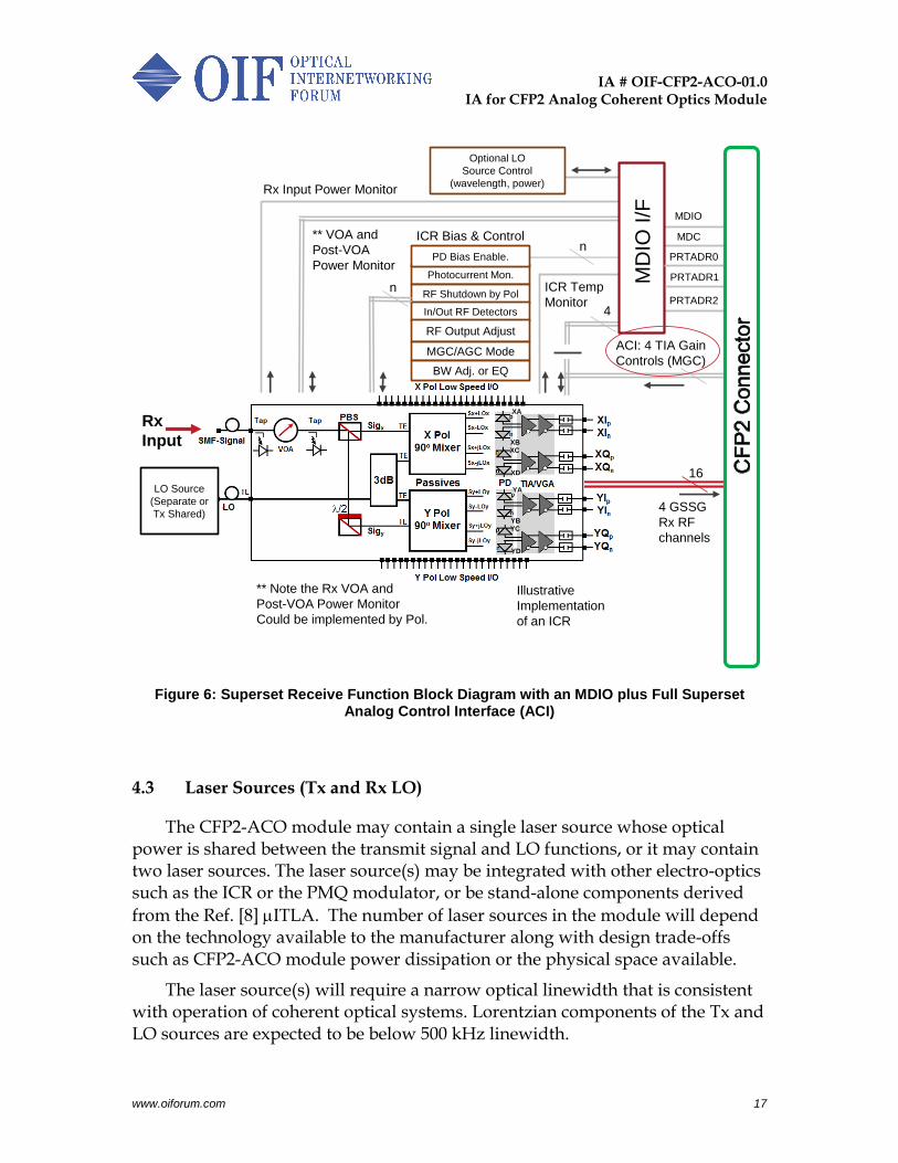
4.2 Receive (Rx) Coherent Optics Function Block Diagrams
The CFP2-ACO receive function block diagram for an MDIO only control interface is shown in Figure 5. The CFP2-ACO receive function block diagram for an MDIO plus Analog Control Interface (ACI) is shown in Figure 6. In both Figures the Rx superset module functionality available on the MDIO control interface is shown. Not all this Rx functionality is required for an IA compatible module. The BB8B Rx Subsystem Features register and the BB8C Rx TIA/VGA Features register provide the user feedback on the functionality available within a given module vendor’s implementation.
MDC
MDIO
PRTADR0
PRTADR1
PRTADR2
Ch. Gain / Current Adjust
Ch. Amp. / Cross Adjust
Ch. RF Output Detector
Ch. Equalization
n
Tx Output Power Monitor
16
Tx Driver [Linear or Limiting]
Driver Ch. Enable
Tx Source Control,
l: gridded, gridless, off-
grid tuning
Tx O
utp
ut
n
D
MDC
MDIO
PRTADR0
PRTADR1
PRTADR2
S.E. or D.E.
Output
Tap
Pol-
Mux
Shutter /
VOA /
SOA /
EDFA
Y Power Control
VOA/SOA
X Power Control
VOA/SOA
Rot
MZ RF Phase
Shifter DC
Bias
(4) S.E. (8) D.E.
X
Y
I
Q
I
QPost Pol.
MuxTap
X Tap
Y Tap
MD
IO I
/F
Laser
Outer MZInner MZ
MD
IO I/FIQ Quadrature Taps [4]
Inner Phase
Shifter Control (8)
(4) Outer Phase
Shifter Control
ACI
4 2
0-15
PM SYNC
41 1 1 1
Temperature
Monitoring:
PMQ, PMQ
Case, Driver
1
4 GSSG Tx RF channels
[with DC Blocks]
Tx Output
Shutter / VOA
/Post-Mod.
Amplifier (SOA
or EDFA)
IA # OIF-CFP2-ACO-01.0
IA for CFP2 Analog Coherent Optics Module
www.oiforum.com 16
Figure 5: Superset Receive Function Block Diagram with an MDIO Only Control Interface
MDC
MDIO
PRTADR0
PRTADR1
PRTADR2
Photocurrent Mon.
RF Shutdown by Pol
In/Out RF Detectors
RF Output Adjust
MGC/AGC Mode
n
** Note the Rx VOA and
Post-VOA Power Monitor
Could be implemented by Pol.
Rx Input Power Monitor
16
4 GSSG
Rx RF
channels
4
ICR Bias & Control
4 TIA
Gain
Control
(GC)
ICR Temp
Monitor
XBXC
XA
XD
YBYC
YA
YD
BW Adj. or EQ
Optional LO
Source Control
(wavelength, power)
** VOA and
Post-VOA
Power Monitor
Rx
Input
n
MD
IO I
/F
LO Source
(Separate or
Tx Shared)
Illustrative
Implementation
of an ICR
PD Bias Enable.
IA # OIF-CFP2-ACO-01.0
IA for CFP2 Analog Coherent Optics Module
www.oiforum.com 17
Figure 6: Superset Receive Function Block Diagram with an MDIO plus Full Superset Analog Control Interface (ACI)
4.3 Laser Sources (Tx and Rx LO)
The CFP2-ACO module may contain a single laser source whose optical power is shared between the transmit signal and LO functions, or it may contain two laser sources. The laser source(s) may be integrated with other electro-optics such as the ICR or the PMQ modulator, or be stand-alone components derived
from the Ref. [8] ITLA. The number of laser sources in the module will depend on the technology available to the manufacturer along with design trade-offs such as CFP2-ACO module power dissipation or the physical space available.
The laser source(s) will require a narrow optical linewidth that is consistent with operation of coherent optical systems. Lorentzian components of the Tx and LO sources are expected to be below 500 kHz linewidth.
MDC
MDIO
PRTADR0
PRTADR1
PRTADR2
Photocurrent Mon.
RF Shutdown by Pol
In/Out RF Detectors
RF Output Adjust
MGC/AGC Mode
n
** Note the Rx VOA and
Post-VOA Power Monitor
Could be implemented by Pol.
Rx Input Power Monitor
16
4 GSSG
Rx RF
channels
4
ICR Bias & Control
ICR Temp
Monitor
XBXC
XA
XD
YBYC
YA
YD
BW Adj. or EQ
Optional LO
Source Control
(wavelength, power)
** VOA and
Post-VOA
Power Monitor
Rx
Input
n
MD
IO I/F
LO Source
(Separate or
Tx Shared)
Illustrative
Implementation
of an ICR
PD Bias Enable.
ACI: 4 TIA Gain
Controls (MGC)
IA # OIF-CFP2-ACO-01.0
IA for CFP2 Analog Coherent Optics Module
www.oiforum.com 18
The channelization of the Tx and LO sources is expected to vary by application, with the most demanding applications requiring compatibility with arbitrary wavelength channel grids having a 6.25 GHz channel spacing.
To enable these applications in Section 12.1, the OIF is requesting registers to implement arbitrary settable Tx/Rx first channel frequencies with a 1 MHz resolution from the CFP2-MSA. The B430 and B440 Fine Tune Frequency registers are also required in the CFP2-ACO (they are not optional.)
4.4 Integrated Polarization Multiplexed Quadrature Mach-Zehnder Modulator (PMQ Modulator)
The PMQ modulator impresses the optical phase modulation onto the Tx CW source output. Electrical drive signals are provided from four modulator RF drivers and may be differential or single-ended, depending on the material and/or design of the optical modulators.
The modulator comprises X and Y polarization paths which are orthogonally polarization multiplexed prior to coupling into the single mode fiber output. Power in the two polarization paths may be balanced by the action of variable optical attenuator (VOA) or semiconductor amplifier (SOA) functions. Prior to launch into the output fiber the total power shall be controlled by a shutter, variable optical attenuator (VOA), or optical amplifier (SOA or EDFA) using associated tap monitoring photodiodes.
The individual Mach-Zehnder (MZ) modulator elements have electrodes that allow the phase imbalance between their arms to be adjusted to maintain optimum system performance over life, wavelength and temperature. Control is facilitated using various in-line and complimentary optical tap monitoring points. CFP2-ACO operating Classes are introduced in Section 5. For Class 1 and Class 2 operation it is expected that all control for bias and imbalance of the MZ elements will be controlled by the module itself, or via the management interface (MDIO). For Class 3 operation the imbalance of the MZ elements can optionally be controlled by the Host using both the MDIO interface and the Analogue Control Interface.
4.5 Intradyne Coherent Receiver (ICR)
The ICR function may be a stand-alone function within the CFP2-ACO or it may be physically integrated with other functions such as an LO source. The
Ref. [7] ICR and the Ref. [13] ICR are anticipated implementations for this function. The Rx optical input signal may be monitored and controlled by optical photodiode tap and VOA functions before or after the polarization de-multiplexing occurs within the ICR.
IA # OIF-CFP2-ACO-01.0
IA for CFP2 Analog Coherent Optics Module
www.oiforum.com 19
The ICR function shall provide Rx optical input polarization de-multiplexing, LO splitting, and 90-degree mixer hybrids feeding eight photodiodes in 4 balanced pairs. Four differential transimpedance amplifiers (TIAs) shall amplify the received X and Y polarization quadrature signals (XI,XQ,YI,YQ) and AC couple them to the CFP2 connector Rx differential signal pairs for return to the Host.
The TIAs in the ICR function enable multiple signal monitors and control methods. The most notable TIA control choice is between an automatic or manual gain control operating mode (AGC or MGC). The TIAs may also facilitate a bandwidth equalization function and provide various input signal strength and/or output level monitors.
In the AGC operating mode there is RF output level adjust control available on the management interface and in the MGC operating mode an external signal is used to control the gain of each differential amplifier. The MGC external gain control can be provided via management interface registers or via the Analogue Control Interface (ACI).
4.6 MZ Modulator RF Drivers
The MZ modulator RF drivers amplify the signals from the Host that are delivered across the CFP2 transmit-side connector interface. They drive the optical MZ modulators at a chosen fraction of 2×Vpi, dependent on the CFP2-ACO operating class and modulation format.
RF drivers are likely to be one of the more highly power dissipative components within the CFP2-ACO module, so they require appropriate heatsinking for long term operation.
The RF drivers may be controlled from the management interface registers and/or their output drive level may be actively controlled. To assist with accurate drive level control the driver function may include output side RF detectors which return mean or peak signal levels.
RF drivers shall provide either a limiting or linear drive transfer characteristic in order to deliver the Class 1 or Class 2&3 operating regimes respectively.
4.7 Optical Power Monitoring and Control
Optical power monitoring and control are key parts of the functionality in the CFP2-ACO module. The electronics within the module must process the various monitoring signals and make them available over the management interface (MDIO) or send them via the Analogue Control Interface (ACI). Example requirements for the power monitoring and control functions include the following:
IA # OIF-CFP2-ACO-01.0
IA for CFP2 Analog Coherent Optics Module
www.oiforum.com 20
Maintain stable total output power.
Adjust output power to match the use situation.
Shutter Tx output power during tuning and set up operations.
Balance X and Y polarization optical powers.
Monitor or adjust modulation depth to suit modulation type.
Maintain modulator imbalance and bias point over time, temperature and wavelength.
Control receiver optical signal level.
Adjust receiver output voltage swing.
Adjust receiver bandwidth or peaking function, if available.
Indicate received signal strength
Alarm on LOS.
4.8 MDIO Management Interface Specification
The Management Data Input/Output interface is the main way of communicating with the CFP2-ACO module. The interface implements a clause 45 compliant IEEE Std. 802.3TM-2012 [8] management data interface that allows control information to be sent to the CFP2-ACO module as required. The MDIO bus carries bidirectional data and the MDC signal is the associated clock. Three hardware port address lines (PRTADR0 to PRTADR2) allow multiple modules to be controlled from a single Host. The MDIO Management Interface Specification (MIS) is detailed in Section 11.
4.9 Electronics
The CFP2-ACO needs to include the necessary electronics to realize communications and control functions for all the electro-optic elements. These electronics will include power supplies with appropriate filtering, control elements such as micro-processors or FPGAs, and bias circuitry for modulator elements and photodiodes. The cumulative power dissipation of all the electronics and electro-optic functions need to be within the specified power dissipation limits for the CFP2-ACO module, provided in Section 6.4.
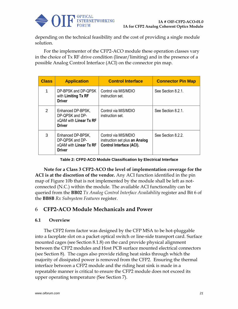
CFP2-ACO Module Classification by Electrical Interface 5
Three broad classes of operation for the CFP2-ACO module are necessary to meet the requirements of users, as shown in Table 2. These operation classes may be realized by a single configurable module or in optimized module types,
IA # OIF-CFP2-ACO-01.0
IA for CFP2 Analog Coherent Optics Module
www.oiforum.com 21
depending on the technical feasibility and the cost of providing a single module solution.
For the implementer of the CFP2-ACO module these operation classes vary in the choice of Tx RF drive condition (linear/limiting) and in the presence of a possible Analog Control Interface (ACI) on the connector pin map.
Class Application Control Interface Connector Pin Map
1 DP-BPSK and DP-QPSK with Limiting Tx RF Driver
Control via MIS/MDIO instruction set.
See Section 8.2.1.
2 Enhanced DP-BPSK, DP-QPSK and DP- xQAM with Linear Tx RF Driver
Control via MIS/MDIO instruction set.
See Section 8.2.1.
3 Enhanced DP-BPSK, DP-QPSK and DP-xQAM with Linear Tx RF Driver
Control via MIS/MDIO instruction set plus an Analog Control Interface (ACI).
See Section 8.2.2.
Table 2: CFP2-ACO Module Classification by Electrical Interface
Note for a Class 3 CFP2-ACO the level of implementation coverage for the ACI is at the discretion of the vendor. Any ACI function identified in the pin map of Figure 10b that is not implemented by the module shall be left as not-connected (N.C.) within the module. The available ACI functionality can be queried from the BB02 Tx Analog Control Interface Availability register and Bit 6 of the BB8B Rx Subsystem Features register.
CFP2-ACO Module Mechanicals and Power 6
6.1 Overview
The CFP2 form factor was designed by the CFP MSA to be hot-pluggable into a faceplate slot on a packet optical switch or line-side transport card. Surface mounted cages (see Section 8.1.8) on the card provide physical alignment between the CFP2 modules and Host PCB surface mounted electrical connectors (see Section 8). The cages also provide riding heat sinks through which the majority of dissipated power is removed from the CFP2. Ensuring the thermal interface between a CFP2 module and the riding heat sink is made in a repeatable manner is critical to ensure the CFP2 module does not exceed its upper operating temperature (See Section 7).
IA # OIF-CFP2-ACO-01.0
IA for CFP2 Analog Coherent Optics Module
www.oiforum.com 22
6.2 Mechanical Dimensions
Normative engineering drawings of the CFP2 form factor, cages and connectors are given in Ref. [11]. Further detail on the mechanical characteristics of the CFP2 housing are given in Ref. [3], which should be read in conjunction with this IA for a successful CFP2-ACO implementation. Table 3 outlines the CFP2-ACO relevant sections in the Ref. [3] CFP-MSA Hardware Specification.
CFP MSA Hardware Specification [Ref 3.]
Topic Comment
Section 5.3 CFP2 Module Dimensions
Simple mechanical outline.
Section 5.3.1
CFP2 Mechanical Surface Characteristics
In addition see Section 7.3 and 7.4 below for recommendations on the CFP2-ACO thermal interface area dimensions, as well as surface flatness and roughness.
Section 5.3.2 CFP2 Insertion & Extraction
Details insertion, extraction and retention forces.
Table 3: CFP2-ACO Relevant CFP-MSA Hardware Specification References
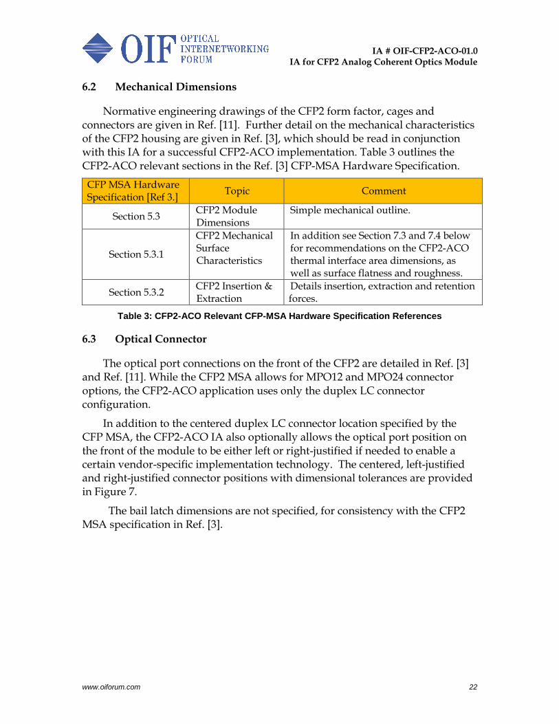
6.3 Optical Connector
The optical port connections on the front of the CFP2 are detailed in Ref. [3] and Ref. [11]. While the CFP2 MSA allows for MPO12 and MPO24 connector options, the CFP2-ACO application uses only the duplex LC connector configuration.
In addition to the centered duplex LC connector location specified by the CFP MSA, the CFP2-ACO IA also optionally allows the optical port position on the front of the module to be either left or right-justified if needed to enable a certain vendor-specific implementation technology. The centered, left-justified and right-justified connector positions with dimensional tolerances are provided in Figure 7.
The bail latch dimensions are not specified, for consistency with the CFP2 MSA specification in Ref. [3].
IA # OIF-CFP2-ACO-01.0
IA for CFP2 Analog Coherent Optics Module
www.oiforum.com 23
Figure 7: CFP2-ACO Allowed Connector Positions (Centered, Left Justified, and Right Justified) with Dimensional Tolerances.
6.4 Module Power Dissipation Classes
The Power Dissipation Classes for CFP2 modules are defined in Section 4.2 of Ref. [3]. The CFP2-ACO shall use these same definitions that range from a maximum total power dissipation of 3 Watts (Power Dissipation Class 1) in 3W increments up to 18 Watts (Power Dissipation Class 6).
Register 807E bits 6-7 provide the Power Dissipation Class for the CFP2-ACO module.
Class 1 CFP2-ACO modules shall be Power Dissipation Class 4 or better, i.e. <12W.
6.5 Module Bail Latch Color
The CFP2-ACO bail latch color shall be a pale orange. One possible implementation would be Pantone 1575C.
IA # OIF-CFP2-ACO-01.0
IA for CFP2 Analog Coherent Optics Module
www.oiforum.com 24
CFP2-ACO Module Thermal Interface Requirements 7
7.1 Data Requirements
The basic thermal data reporting requirements for the CFP2 ACO module, following Ref. [12], are as follows:
a) Maximum Power Dissipation at EOL Long Term Operating Case Temperature b) Maximum Power Dissipation at EOL Short-Term Operating Case Temperature c) Minimum Power Dissipation at BOL Short-Term Operating Case Temperature d) Monitor Point Location within the Thermal Interface Area e) Maximum Long-Term Operating Temperature at the Monitor Point f) Maximum Short-Term Operating Temperature at the Monitor Point g) Minimum Operating Temperature at the Monitor Point h) Thermal Interface Resistance i) Surface Flatness of the Thermal Interface Area j) Surface Roughness across the Thermal Interface Area
7.2 Thermal Environment
To define the thermal interface requirements, the CFP2-ACO thermal environment is assumed to be that of a shelf level product, as defined by Telcordia NEBS requirements in Ref. [14], with 55°C ambient air, corresponding to a 70°C or greater Monitor Point maximum temperature for short-term operation.
7.3 Thermal Interface Area
For a Power Dissipation Class 4 CFP2-ACO module (<12W) the Power Density Class of the module is pd05 (<0.5W/cm2), as defined in Ref. [12].
The top surface of the CFP2-ACO module that lies directly under the cage opening shall be dimensionally controlled to enable a good thermal interface with the riding heat sink. The thermal interface area is defined in Section 7.2 of Ref. [12] as the heat transfer contact area between the module and heat sink, centered with respect to the cage opening, but typically at most 0.5 mm less in width, and 2 mm less in depth.
In Ref. [3] an example cage opening of 37.8 mm wide x 71 mm deep is provided for the generic CFP2 module. It is recommended that this cage opening be maximized for the CFP2-ACO application using the cage design principles implemented for the CFP4 Baseline Design Rev. R available at Ref. [1].
The normal force between the heat sink and the CFP2 ACO module is limited to 15N as specified in Ref [3].
IA # OIF-CFP2-ACO-01.0
IA for CFP2 Analog Coherent Optics Module
www.oiforum.com 25
7.4 Module Thermal Interface Surface Requirements
To ensure good repeatable heat sink performance it is recommended that the CFP2-ACO thermal interface area have flatness ≤ 0.08 mm and a surface finish ≤0.8 µm Ra. This is to ensure that system designers can provide adequate cooling for modules with similar or better heat sink contact surface preparation. The goal is to have an overall thermal interface resistance of <2 °C-cm2/W, as defined in Ref. [12].
7.5 Thermal Sensor Calibration
The CFP2 ACO internal temperature sensor is to be calibrated to report the temperature at the monitor point with >95% of the heat removed through the heat sink. This implies that the CFP2 module is in thermal equilibrium with the cage and PCB so that little net heat is transferred in or out of locations other than the thermal interface area.
CFP2-ACO Electrical Connector Interface 8
8.1 104-Pin Electrical Connector
8.1.1 Background
The Plug and Host connector parts for the CFP2 are detailed in the CFP MSA Ref. [3]. The Plug is the male connector part attached to the CFP2-ACO module PCB. The Host Connector is the female connector part that is located at the rear of the CFP2 cage, attached to the line or switch card. The female Host Connector is covered by a Host Connector Cover Assembly that includes gaskets around the opening for the Plug connector to provide electromagnetic shielding.
Both connector parts are of a molded polymer construction with plated metal contact inserts. The contact pitch is 0.6mm and there are 104 contacts.
Performance characterization of several connector implementations in provided in Appendix I.
IA # OIF-CFP2-ACO-01.0
IA for CFP2 Analog Coherent Optics Module
www.oiforum.com 26
8.1.2 Photographs of Connector: Plug and Host
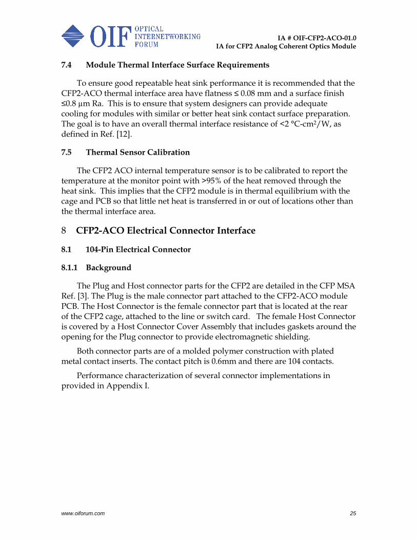
Representative examples of both the Plug and Host Connector parts are provided in Figure 8.
Figure 8 : (a) Plug bottom side showing sequenced connection contacts, (b) Plug top side showing GSSG format RF contact groups, (c) Host Connector rear view – pins connected
to Host PCBs, (d) Host Connector front view – accepts the Plug.
8.1.3 Suppliers and Example Part Numbers
At the time of publication there are three suppliers of the connector for the CFP2-ACO. The suppliers listed in alphabetical order and example connector part numbers are given in Table 4 for reference. It is the responsibility of the connector users to ensure that an appropriate part and plating finish is specified for their requirements.
Supplier Example Plug Part Number
Example Host Part Number
Comments
Amphenol P-U56-B104-XXXX P-U99-B104-XXXX -XXXX represents plating thickness, packaging and other options
TE Connectivity 2274844-1 2274845-1
Yamaichi Electronics CN121P-104-0003
CN121P-104-1003
CN121S-104-0001
CN121S-104-1001
-000X are the Standard Performance version (28G). -100X are the High Performance version (56G). These part numbers come with tray packaging. Different packaging option and plug PCB thickness options are available.
Other Add details when available
Table 4: CFP2 Connector Suppliers and Part Numbers
(a) (b)
(c) (d)
IA # OIF-CFP2-ACO-01.0
IA for CFP2 Analog Coherent Optics Module
www.oiforum.com 27
8.1.4 Reliability and Environmental Test Documentation
At the time of publication the reliability documents given in Table 5 are available from the respective suppliers. The listed suppliers have completed and passed the mixed flowing gas test requirements of GR-1217-CORE.
Supplier Document Date Qualification Target
Amphenol QTP9300537 28th February 2014 GR-1217-CORE
Yamaichi Electronics
RE-5354. CN121 Series Evaluation Test Report
31st January 2013 GR-1217-CORE
Other 1
Other 2
Table 5: CFP2 Connector Reliability Documents
8.1.5 Connector Ratings
The current rating per contact pin for the various connectors is given in Table 6 along with the voltage rating and the allowed number of mating cycles.
Supplier Current Capacity per
Pin (mA)
Voltage Rating per pin (V) Rated Mating Cycles
Amphenol 1875 TBC <=200
Yamaichi Electronics
1250 120 <=200
Other 1
Other 2
Table 6: CFP2 Connector Ratings
8.1.6 RF Path S-Parameters
Informative reference data is provided in Appendix I (Section 17).
8.1.7 Connector Cross Mating
This is the subject of further study at the time of publication.
8.1.8 Related CFP2 Cage Products
Manufacturers supply the hardware for single and/or dual CFP2 PCB mounting cages to facilitate the manufacture of line cards, switch cards, or module compliance boards (MCB).
IA # OIF-CFP2-ACO-01.0
IA for CFP2 Analog Coherent Optics Module
www.oiforum.com 28
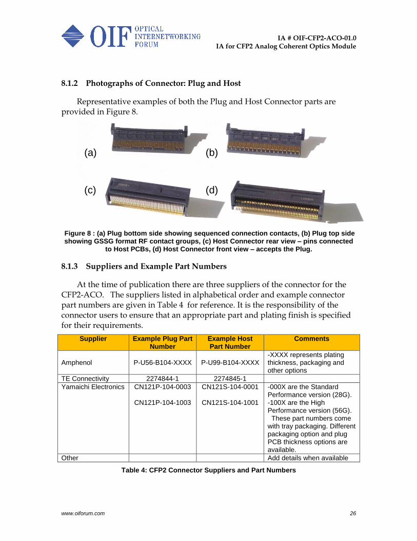
Figure 9: Single CFP2 Cage Illustration (informative).
Some informative part numbers are given in Table 7 and an example of a single CFP2 mounting cage is shown in Figure 9. It is left to the user to ensure that they specify the correct part variant and options for their requirements.
Supplier Single Slot Cage Dual Slot Cage Comments
Amphenol P-U98-B1XX-X0XX P-U98-B2XX-X0XX
Yamaichi Electronics CN121A-104-0003 CN121A-104-0004
TE Connectivity 2274842-1
2287075-1 Cage kits including cage/receptacle/cover
Other 1
Table 7: Related CFP2 Cage Part Numbers
8.2 Electrical Pin Maps
8.2.1 Class 1 and Class 2 Electrical Pin Map
The Class 1 and Class 2 CFP2-ACO module electrical pin map is given in Figure 10a. The pin-out changes in Figure 10a relative to the “Top/Bottom” pin allocation in Ref. [4] are identified by an asterisk on the pin number. These changes include the following: MCLK outputs shall be N.C. within the module; REFCLK inputs shall be appropriately terminated inside the CFP2-ACO, although for Class 2 these inputs can be optionally N.C in the module; the CFP2 4x25G RX0-3 and TX0-3 data pins shall be mapped to the coherent Tx/Rx channels as outlined in Section 8.3. In Figure 10a the [0,0,0] Tx/Rx channel mapping is used for illustrative purposes.
The Class 1 and Class 2 CFP2-ACO module electrical pin map does not impede the Host implementing a CFP2 “universal slot” compatible with both the CFP2-ACO and any selected set of the CFP2 client module electrical interfaces given in Ref. [4].
IA # OIF-CFP2-ACO-01.0
IA for CFP2 Analog Coherent Optics Module
www.oiforum.com 29
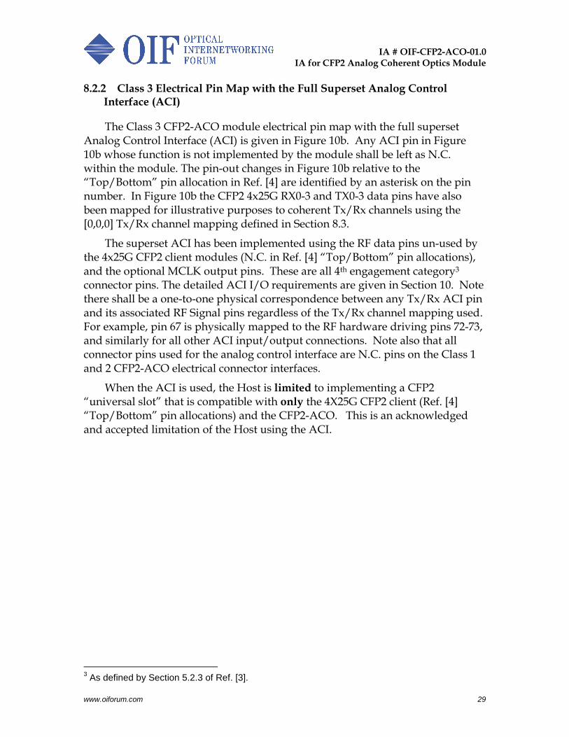
8.2.2 Class 3 Electrical Pin Map with the Full Superset Analog Control Interface (ACI)
The Class 3 CFP2-ACO module electrical pin map with the full superset Analog Control Interface (ACI) is given in Figure 10b. Any ACI pin in Figure 10b whose function is not implemented by the module shall be left as N.C. within the module. The pin-out changes in Figure 10b relative to the “Top/Bottom” pin allocation in Ref. [4] are identified by an asterisk on the pin number. In Figure 10b the CFP2 4x25G RX0-3 and TX0-3 data pins have also been mapped for illustrative purposes to coherent Tx/Rx channels using the [0,0,0] Tx/Rx channel mapping defined in Section 8.3.
The superset ACI has been implemented using the RF data pins un-used by the 4x25G CFP2 client modules (N.C. in Ref. [4] “Top/Bottom” pin allocations), and the optional MCLK output pins. These are all 4th engagement category3 connector pins. The detailed ACI I/O requirements are given in Section 10. Note there shall be a one-to-one physical correspondence between any Tx/Rx ACI pin and its associated RF Signal pins regardless of the Tx/Rx channel mapping used. For example, pin 67 is physically mapped to the RF hardware driving pins 72-73, and similarly for all other ACI input/output connections. Note also that all connector pins used for the analog control interface are N.C. pins on the Class 1 and 2 CFP2-ACO electrical connector interfaces.
When the ACI is used, the Host is limited to implementing a CFP2 “universal slot” that is compatible with only the 4X25G CFP2 client (Ref. [4] “Top/Bottom” pin allocations) and the CFP2-ACO. This is an acknowledged and accepted limitation of the Host using the ACI.
3 As defined by Section 5.2.3 of Ref. [3].
IA # OIF-CFP2-ACO-01.0
IA for CFP2 Analog Coherent Optics Module
www.oiforum.com 30
Figure 10 (a) Class 1 and 2 Electrical Pin Map, (b) Class 3 Full Superset ACI Interface Electrical Pin Map.
CFP2-ACO CFP2-ACO Toward Host CFP2-ACO CFP2-ACO
Bottom: Class 1/2 Top: Class 1/2 Bottom: Class 3 Top: Class 3
1 GND 104 GND pin 1 GND 104 GND
2* N.C. 103 N.C. view 2*X OUTER PHASE DITHER(RF Mapping [0,0,0])
103*XI PHASE DITHER (RF Mapping [0,0,0])
3* N.C. 102 N.C. from 3*Y OUTER PHASE DITHER(RF Mapping [0,0,0])
102 N.C.
4 GND 101 GND top 4 GND 101 GND
5 N.C. 100* TX_XIp (RF Mapping [0,0,0]) 5*TX X POL. TAP(RF Mapping [0,0,0])
100* TX_XIp (RF Mapping [0,0,0])
6 N.C. 99* TX_XIn (RF Mapping [0,0,0]) 6*TX Y POL. TAP(RF Mapping [0,0,0])
99* TX_XIn (RF Mapping [0,0,0])
7 3.3V_GND 98 GND GND 7 3.3V_GND 98 GND
8 3.3V_GND 97* TX_XQp (RF Mapping [0,0,0]) RF Signal 8 3.3V_GND 97* TX_XQp (RF Mapping [0,0,0])
9 3.3V 96* TX_XQn (RF Mapping [0,0,0]) 3.3V Supply 9 3.3V 96* TX_XQn (RF Mapping [0,0,0])
10 3.3V 95 GND Vendor IO pins 10 3.3V 95 GND
11 3.3V 94 N.C. MSA Pins 11 3.3V 94 N.C.
12 3.3V 93 N.C. ACI-Input 12 3.3V 93*XQ PHASE DITHER(RF Mapping [0,0,0])
13 3.3V_GND 92 GND ACI-Output 13 3.3V_GND 92 GND
14 3.3V_GND 91 N.C. 14 3.3V_GND 91*YI PHASE DITHER (RF Mapping [0,0,0])
15 VND_IO_A 90 N.C. 15 VND_IO_A 90 N.C.
16 VND_IO_B 89 GND 16 VND_IO_B 89 GND
17 PRG_CNTL1 88* TX_YIp (RF Mapping [0,0,0]) 17 PRG_CNTL1 88* TX_YIp (RF Mapping [0,0,0])
18 PRG_CNTL2 87* TX_YIn (RF Mapping [0,0,0]) 18 PRG_CNTL2 87* TX_YIn (RF Mapping [0,0,0])
19 PRG_CNTL3 86 GND 19 PRG_CNTL3 86 GND
20 PRG_ALRM1 85* TX_YQp (RF Mapping [0,0,0]) 20 PRG_ALRM1 85* TX_YQp (RF Mapping [0,0,0])
21 PRG_ALRM2 84* TX_YQn (RF Mapping [0,0,0]) 21 PRG_ALRM2 84* TX_YQn (RF Mapping [0,0,0])
22 PRG_ALRM3 83 GND 22 PRG_ALRM3 83 GND
23 GND 82 N.C. 23 GND 82 N.C.
24 TX_DIS 81 N.C. 24* TX_DIS (PRG_CNTL) 81*YQ PHASE DITHER(RF Mapping [0,0,0])
25 RX_LOS 80 GND 25* RX_LOS (PRG_ALRM) 80 GND
26 MOD_LOPWR 79* REFCLKn-Terminated in ACO^ 26 MOD_LOPWR 79* REFCLKn - N.C. in ACO
27 MOD_ABS 78* REFCLKp-Terminated in ACO^ 27 MOD_ABS 78* REFCLKp - N.C. in ACO
28 MOD_RSTn 77 GND 28 MOD_RSTn 77 GND
29 GLB_ALRMn 76 N.C. 29 GLB_ALRMn 76*TX X-POL POWER DITHER(RF Mapping [0,0,0])
30 GND 75 N.C. 30 GND 75*TX Y-POL POWER DITHER(RF Mapping [0,0,0])
31 MDC 74 GND 31 MDC 74 GND
32 MDIO 73* RX_XIp (RF Mapping [0,0,0]) 32 MDIO 73* RX_XIp (RF Mapping [0,0,0])
33 PRTADR0 72* RX_XIn (RF Mapping [0,0,0]) 33 PRTADR0 72* RX_XIn (RF Mapping [0,0,0])
34 PRTADR1 71 GND 34 PRTADR1 71 GND
35 PRTADR2 70* RX_XQp (RF Mapping [0,0,0]) 35 PRTADR2 70* RX_XQp (RF Mapping [0,0,0])
36 VND_IO_C 69* RX_XQn (RF Mapping [0,0,0]) 36 VND_IO_C 69* RX_XQn (RF Mapping [0,0,0])
37 VND_IO_D 68 GND 37 VND_IO_D 68 GND
38 VND_IO_E 67 N.C. 38 VND_IO_E 67* Rx MGC XI (RF Mapping [0,0,0])
39 3.3V_GND 66 N.C. 39 3.3V_GND 66* Rx MGC XQ (RF Mapping [0,0,0])
40 3.3V_GND 65 GND 40 3.3V_GND 65 GND
41 3.3V 64 N.C. 41 3.3V 64* Rx MGC YI (RF Mapping [0,0,0])
42 3.3V 63 N.C. 42 3.3V 63* Rx MGC YQ (RF Mapping [0,0,0])
43 3.3V 62 GND 43 3.3V 62 GND
44 3.3V 61* RX_YIp (RF Mapping [0,0,0]) 44 3.3V 61* RX_YIp (RF Mapping [0,0,0])
45 3.3V_GND 60* RX_YIn (RF Mapping [0,0,0]) 45 3.3V_GND 60* RX_YIn (RF Mapping [0,0,0])
46 3.3V_GND 59 GND 46 3.3V_GND 59 GND
47 N.C. 58* RX_YQp (RF Mapping [0,0,0]) 47* TX XI TAP (RF Mapping [0,0,0]) 58* RX_YQp (RF Mapping [0,0,0])
48 N.C. 57* RX_YQn (RF Mapping [0,0,0]) 48* TX XQ TAP (RF Mapping [0,0,0]) 57* RX_YQn (RF Mapping [0,0,0])
49 GND 56 GND 49 GND 56 GND
50* N.C. 55 N.C. 50* TX YI TAP (RF Mapping [0,0,0]) 55* N.C.
51* N.C. 54 N.C. 51* TX YQ TAP (RF Mapping [0,0,0]) 54* TX POST POL. MUX TAP
52 GND 53 GND 52 GND 53 GND
^ For Class 2 Modules the Host REFCLK inputs can be optionally N.C. within the CFP2-ACO.
The (RF Mapping [0,0,0]) label on all ACI pins means that a one-to-one physical correspondence is maintained
between a Tx/Rx ACI pin and its associated RF Signal pins regardless of the Tx/Rx channel mapping used.
-E.g. pin 67 is physically mapped to the RF hardware driving pins 72-73 and similarly for all other Tx/Rx ACI connections.
IA # OIF-CFP2-ACO-01.0
IA for CFP2 Analog Coherent Optics Module
www.oiforum.com 31
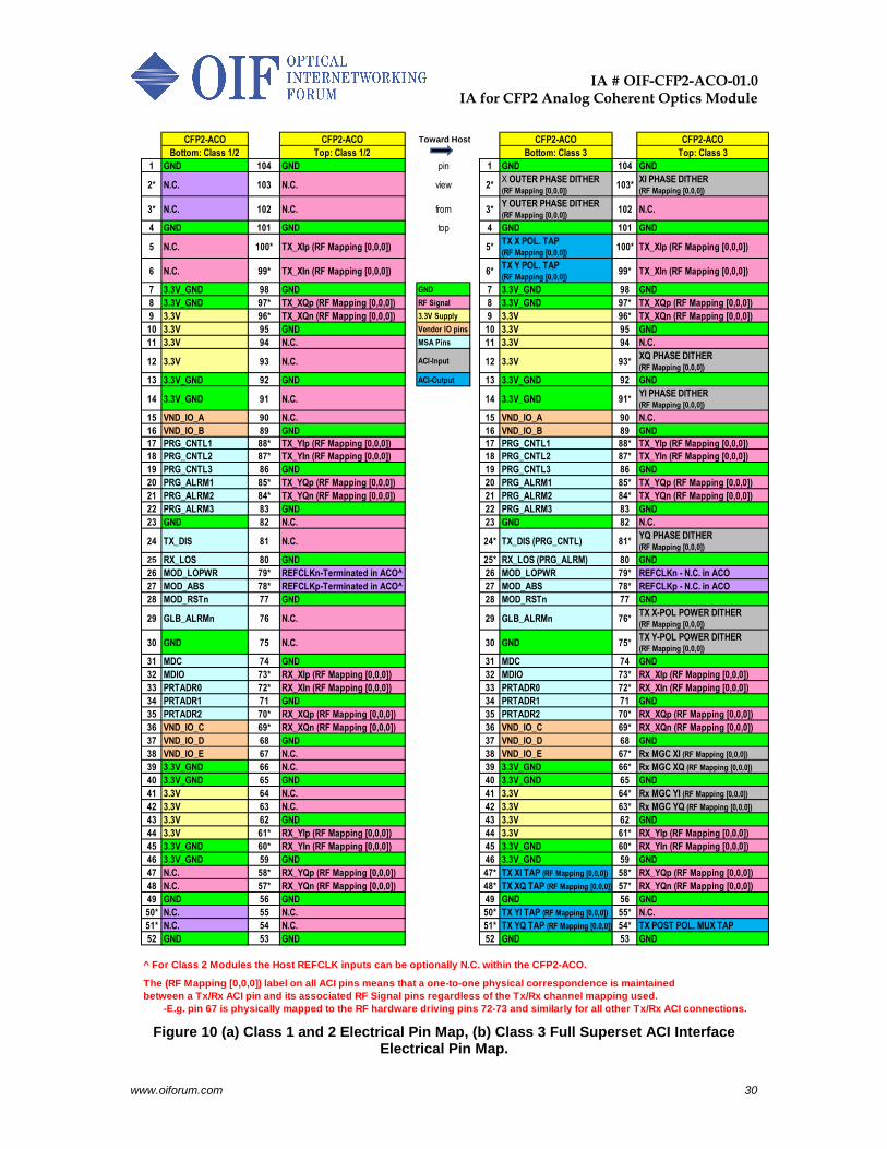
8.3 Allowed Tx and Rx RF Channel Mappings
X and Y indicate a pair of mutually orthogonal polarizations of any orientation and I and Q are mutually orthogonal phase channels in each polarization. The four data path channels are therefore labeled XI, XQ, YI, and YQ. The complementary electrical outputs for each channel are labeled ‘p’ and ‘n’.
All coherent channel mappings provided in Table 8 are independent possible mappings for the Tx and Rx RF connector interfaces. The user can identify the mapping used by the module through the BB00 Tx RF Channeling Mapping register and the BB8A Rx RF Channel Mapping register.
A Tx or Rx mapping is specified in Table 8 by three designations: [X:Y ; I,Q ; p/n], where a “:” is used to separate X&Y, a “,” is used to separate I&Q, and a “/” is used to separate p&n. In Table 8 red text shows where the mapping flips occur relative to the 1st row in each group. Tx coherent channel mappings read left-to-right in Table 8 correspond to electrical connector pins 100, 99, 97, 96, 88, 87, 85, and 84. Rx coherent channel mappings read left-to-right in Table 8 correspond to electrical connector pins: 73, 72, 70, 69, 61, 60, 58, and 57. It is important to highlight that Table 8 does not allow interleaving of the channels by polarization since this would add a non-essential level of complexity to the Tx and Rx digital processing. Except for BB00 and BB8A, all MDIO register name and register bit definitions for the XI, XQ, YI, and YQ channels are independent of and unaffected by the channel-to-connector pin mappings in Table 8.
Mapping X:Y I,Q p/n Notes [0,x,x] X:Y Pol. cannot be interleaved [1,x,x] Y:X [x,0,x] I,Q:I,Q Same across Pol. [x,1,x] Q,I:Q,I [x,2,x] I,Q:Q,I Flip across Pol. [x,3,x] Q,I:I,Q [x,x,0] p/n,p/n:p/n,p/n Same across Pol. and I,Q [x,x,1] n/p,n/p:n/p,n/p [x,x,2] p/n,p/n:n/p,n/p Flip across Pol. [x,x,3] n/p,n/p:p/n,p/n [x,x,4] p/n,n/p:p/n,n/p Flip across I,Q [x,x,5] n/p,p/n:n/p,p/n [x,x,6] p/n,n/p:n/p,p/n Flip across Pol. and I,Q [x,x,7] n/p,p/n:p/n,n/p
Table 8: Tx and Rx RF Channel Mappings on the Electrical Connector Interface
IA # OIF-CFP2-ACO-01.0
IA for CFP2 Analog Coherent Optics Module
www.oiforum.com 32
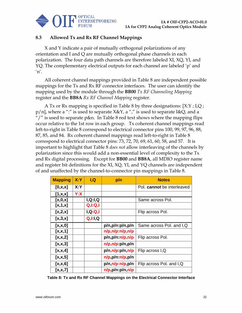
I and Q are established by the heterodyne technique, with the frequency of the Signal input to the receiver greater than the frequency of the LO input. The I and Q channel outputs are measured in the time domain.
Under these conditions the Signal Q channel phase lags by nominally +90 degrees the Signal I channel phase, as shown in Figure 11.
Figure 11: I and Q Phase Definitions
Outputs ‘p’ and ‘n’ are the complementary outputs for each channel and are such that the output voltage for ‘p’ increases as the Signal and Local Oscillator approach the in-phase condition to form constructive interference, and the output voltage for ‘n’ decreases under the same condition.
CFP2-ACO Tx and Rx RF Electrical Interfaces 9
9.1 Introduction
The Tx and Rx RF interfaces on the CFP2 connector are each GSSG X4 RF interfaces on a 0.6 mm pin pitch. The CFP2 client 4x25G RX0-3 and the 4x25G TX0-3 data lanes are mapped in the CFP2-ACO to the coherent channels as specified in Section 8.3.
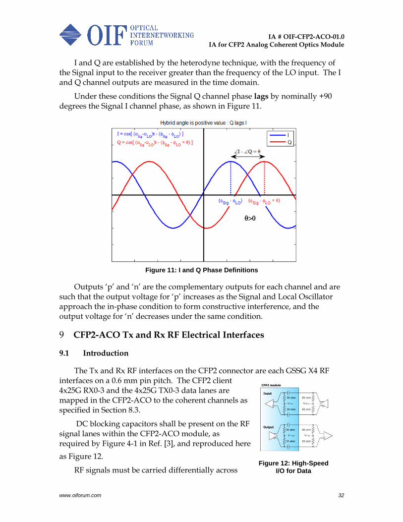
DC blocking capacitors shall be present on the RF signal lanes within the CFP2-ACO module, as required by Figure 4-1 in Ref. [3], and reproduced here
as Figure 12.
RF signals must be carried differentially across Figure 12: High-Speed
I/O for Data
IA # OIF-CFP2-ACO-01.0
IA for CFP2 Analog Coherent Optics Module
www.oiforum.com 33
the CFP2 connector interface to achieve acceptable levels of crosstalk. The Host is therefore agnostic to the PMQ modulator RF drive design (differential or series push-pull). The CFP2-ACO RF electrical interface requirements do not limit modulator technology choices.
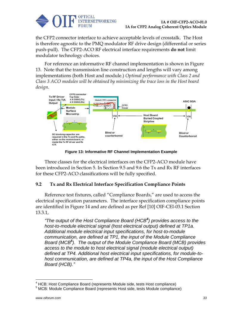
For reference an informative RF channel implementation is shown in Figure 13. Note that the transmission line construction and lengths will vary among implementations (both Host and module.) Optimal performance with Class 2 and Class 3 ACO modules will be obtained by minimizing the trace loss in the Host board design.
Figure 13: Informative RF Channel Implementation Example
Three classes for the electrical interfaces on the CFP2-ACO module have been introduced in Section 5. In Section 9.5 and 9.6 the Tx and Rx RF interfaces for these CFP2-ACO classifications will be fully specified.
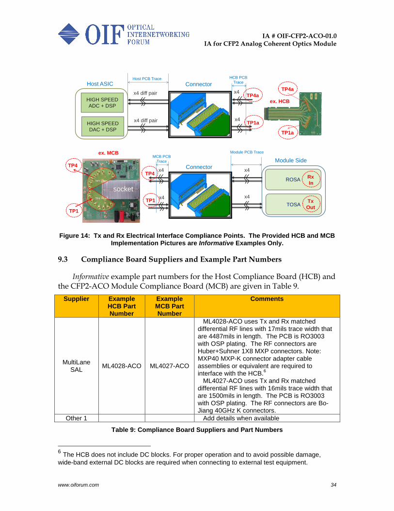
9.2 Tx and Rx Electrical Interface Specification Compliance Points
Reference test fixtures, called “Compliance Boards,” are used to access the electrical specification parameters. The interface specification compliance points are identified in Figure 14 and are defined as per Ref [10] OIF-CEI-03.1 Section 13.3.1,
“The output of the Host Compliance Board (HCB4) provides access to the host-to-module electrical signal (host electrical output) defined at TP1a. Additional module electrical input specifications, for host-to-module communication, are defined at TP1, the input of the Module Compliance Board (MCB5). The output of the Module Compliance Board (MCB) provides access to the module to host electrical signal (module electrical output) defined at TP4. Additional host electrical input specifications, for module-to-host communication, are defined at TP4a, the input of the Host Compliance Board (HCB).”
4 HCB: Host Compliance Board (represents Module side, tests Host compliance)
5 MCB: Module Compliance Board (represents Host side, tests Module compliance)
IA # OIF-CFP2-ACO-01.0
IA for CFP2 Analog Coherent Optics Module
www.oiforum.com 34
Figure 14: Tx and Rx Electrical Interface Compliance Points. The Provided HCB and MCB Implementation Pictures are Informative Examples Only.
9.3 Compliance Board Suppliers and Example Part Numbers
Informative example part numbers for the Host Compliance Board (HCB) and the CFP2-ACO Module Compliance Board (MCB) are given in Table 9.
Supplier Example HCB Part Number
Example MCB Part Number
Comments
MultiLane SAL
ML4028-ACO ML4027-ACO
ML4028-ACO uses Tx and Rx matched differential RF lines with 17mils trace width that are 4487mils in length. The PCB is RO3003 with OSP plating. The RF connectors are Huber+Suhner 1X8 MXP connectors. Note: MXP40 MXP-K connector adapter cable assemblies or equivalent are required to interface with the HCB.
6
ML4027-ACO uses Tx and Rx matched differential RF lines with 16mils trace width that are 1500mils in length. The PCB is RO3003 with OSP plating. The RF connectors are Bo-Jiang 40GHz K connectors.
Other 1 Add details when available
Table 9: Compliance Board Suppliers and Part Numbers
6 The HCB does not include DC blocks. For proper operation and to avoid possible damage,
wide-band external DC blocks are required when connecting to external test equipment.
HIGH SPEED
ADC + DSP
HIGH SPEED
DAC + DSP
Host ASIC
x4 diff pair x4
Connector
TP4a
Host PCB Trace HCB PCB
Trace
TP1a
Module Side
ROSA
TOSA
x4
x4
x4
Connectorx4
x4
MCB PCB
Trace
TP4
TP1
Module PCB Trace
x4 diff pair
ex. HCB
ex. MCB
TP4
TP1
TP4a
TP1a
Rx
In
Tx
Out
socket

IA # OIF-CFP2-ACO-01.0
IA for CFP2 Analog Coherent Optics Module
www.oiforum.com 35
9.4 Compliance Board S Parameter Requirements
Use of compliance boards for testing is assumed for the electrical interface specifications given in Section 9.5 and 9.6.
The mated compliance boards used to measure the CFP2-ACO Module and Host should conform to the S parameter requirements of Annex B (Section 16), with the individual reference MCB and HCB compliance board PCB traces in the mated pair conforming to the differential insertion loss equations provided by Annex A (Section 15).
If compliance boards do not meet the specified S-parameters in Annex A then test results shall be corrected for the difference. The mated MCB-HCB compliance boards S-parameters provided in Annex B are defined between the reference planes of the RF coax connectors.
IA # OIF-CFP2-ACO-01.0
IA for CFP2 Analog Coherent Optics Module
www.oiforum.com 36
9.5 Class 1: RF Electrical Interface Specifications
9.5.1 Class 1: Tx RF Interface Specifications
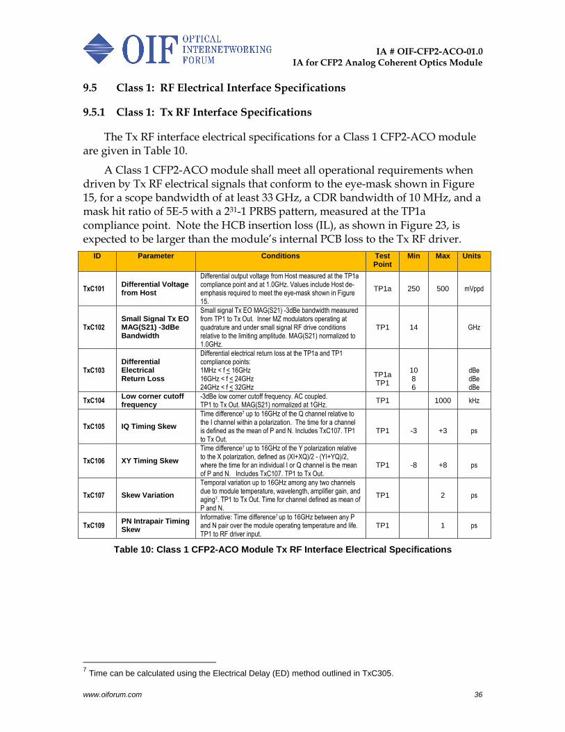
The Tx RF interface electrical specifications for a Class 1 CFP2-ACO module are given in Table 10.
A Class 1 CFP2-ACO module shall meet all operational requirements when driven by Tx RF electrical signals that conform to the eye-mask shown in Figure 15, for a scope bandwidth of at least 33 GHz, a CDR bandwidth of 10 MHz, and a mask hit ratio of 5E-5 with a 231-1 PRBS pattern, measured at the TP1a compliance point. Note the HCB insertion loss (IL), as shown in Figure 23, is expected to be larger than the module’s internal PCB loss to the Tx RF driver.
ID Parameter Conditions Test Point
Min Max Units
TxC101 Differential Voltage from Host
Differential output voltage from Host measured at the TP1a compliance point and at 1.0GHz. Values include Host de-emphasis required to meet the eye-mask shown in Figure 15.
TP1a 250 500 mVppd
TxC102 Small Signal Tx EO MAG(S21) -3dBe Bandwidth
Small signal Tx EO MAG(S21) -3dBe bandwidth measured from TP1 to Tx Out. Inner MZ modulators operating at quadrature and under small signal RF drive conditions relative to the limiting amplitude. MAG(S21) normalized to 1.0GHz.
TP1 14 GHz
TxC103 Differential Electrical Return Loss
Differential electrical return loss at the TP1a and TP1 compliance points: 1MHz < f < 16GHz 16GHz < f < 24GHz 24GHz < f < 32GHz
TP1a TP1
10 8 6
dBe dBe dBe
TxC104 Low corner cutoff frequency
-3dBe low corner cutoff frequency. AC coupled. TP1 to Tx Out. MAG(S21) normalized at 1GHz.
TP1 1000 kHz
TxC105 IQ Timing Skew
Time difference7 up to 16GHz of the Q channel relative to the I channel within a polarization. The time for a channel is defined as the mean of P and N. Includes TxC107. TP1 to Tx Out.
TP1
-3
+3
ps
TxC106 XY Timing Skew
Time difference7 up to 16GHz of the Y polarization relative to the X polarization, defined as (XI+XQ)/2 - (YI+YQ)/2, where the time for an individual I or Q channel is the mean of P and N. Includes TxC107. TP1 to Tx Out.
TP1
-8
+8
ps
TxC107 Skew Variation
Temporal variation up to 16GHz among any two channels due to module temperature, wavelength, amplifier gain, and aging7. TP1 to Tx Out. Time for channel defined as mean of P and N.
TP1 2 ps
TxC109 PN Intrapair Timing Skew
Informative: Time difference7 up to 16GHz between any P and N pair over the module operating temperature and life. TP1 to RF driver input.
TP1 1 ps
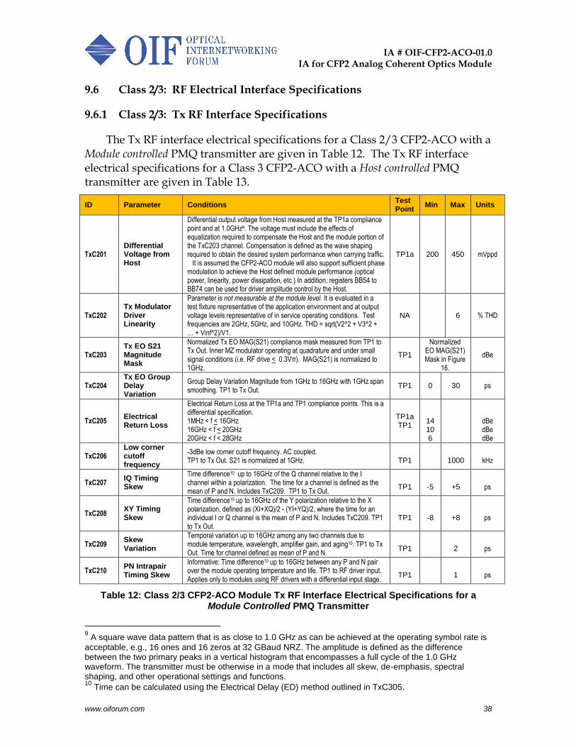
Table 10: Class 1 CFP2-ACO Module Tx RF Interface Electrical Specifications
7 Time can be calculated using the Electrical Delay (ED) method outlined in TxC305.
IA # OIF-CFP2-ACO-01.0
IA for CFP2 Analog Coherent Optics Module
www.oiforum.com 37
0
Y1
-Y1
Y2
-Y2
0 X1 X2 1-X2 1-X1 1Normalized Time (UI)
Vo
lta
ge
(m
V)
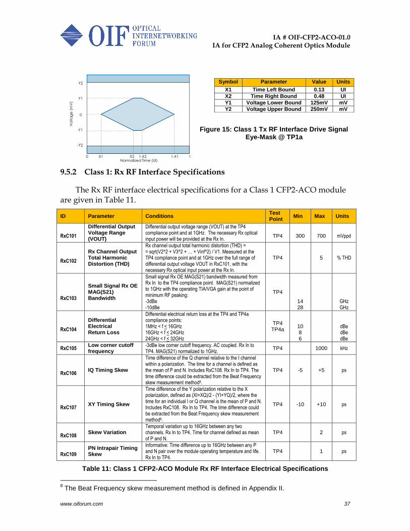
Figure 15: Class 1 Tx RF Interface Drive Signal Eye-Mask @ TP1a
9.5.2 Class 1: Rx RF Interface Specifications
The Rx RF interface electrical specifications for a Class 1 CFP2-ACO module are given in Table 11.
ID Parameter Conditions Test Point
Min Max Units
RxC101
Differential Output Voltage Range (VOUT)
Differential output voltage range (VOUT) at the TP4 compliance point and at 1GHz. The necessary Rx optical input power will be provided at the Rx In.
TP4
300
700
mVppd
RxC102
Rx Channel Output Total Harmonic Distortion (THD)
Rx channel output total harmonic distortion (THD) = = sqrt(V2^2 + V3^2 + … + Vinf^2) / V1. Measured at the TP4 compliance point and at 1GHz over the full range of differential output voltage VOUT in RxC101, with the necessary Rx optical input power at the Rx In.
TP4 5 % THD
RxC103
Small Signal Rx OE MAG(S21) Bandwidth
Small signal Rx OE MAG(S21) bandwidth measured from Rx In to the TP4 compliance point. MAG(S21) normalized to 1GHz with the operating TIA/VGA gain at the point of minimum RF peaking: -3dBe -10dBe
TP4
14 28
GHz GHz
RxC104
Differential Electrical Return Loss
Differential electrical return loss at the TP4 and TP4a compliance points: 1MHz < f < 16GHz 16GHz < f < 24GHz 24GHz < f < 32GHz
TP4 TP4a
10 8 6
dBe dBe dBe
RxC105 Low corner cutoff frequency
-3dBe low corner cutoff frequency. AC coupled. Rx In to TP4. MAG(S21) normalized to 1GHz.
TP4 1000 kHz
RxC106
IQ Timing Skew
Time difference of the Q channel relative to the I channel within a polarization. The time for a channel is defined as the mean of P and N. Includes RxC108. Rx In to TP4. The time difference could be extracted from the Beat Frequency skew measurement method8.
TP4 -5 +5 ps
RxC107
XY Timing Skew
Time difference of the Y polarization relative to the X polarization, defined as (XI+XQ)/2 - (YI+YQ)/2, where the time for an individual I or Q channel is the mean of P and N. Includes RxC108. Rx In to TP4. The time difference could be extracted from the Beat Frequency skew measurement method8.
TP4 -10 +10 ps
RxC108
Skew Variation Temporal variation up to 16GHz between any two channels. Rx In to TP4. Time for channel defined as mean of P and N.
TP4 2 ps
RxC109
PN Intrapair Timing Skew
Informative: Time difference up to 16GHz between any P and N pair over the module operating temperature and life. Rx In to TP4.
TP4 1 ps
Table 11: Class 1 CFP2-ACO Module Rx RF Interface Electrical Specifications
8 The Beat Frequency skew measurement method is defined in Appendix II.
Symbol Parameter Value Units
X1 Time Left Bound 0.13 UI
X2 Time Right Bound 0.48 UI
Y1 Voltage Lower Bound 125mV mV
Y2 Voltage Upper Bound 250mV mV
IA # OIF-CFP2-ACO-01.0
IA for CFP2 Analog Coherent Optics Module
www.oiforum.com 38
9.6 Class 2/3: RF Electrical Interface Specifications
9.6.1 Class 2/3: Tx RF Interface Specifications
The Tx RF interface electrical specifications for a Class 2/3 CFP2-ACO with a Module controlled PMQ transmitter are given in Table 12. The Tx RF interface electrical specifications for a Class 3 CFP2-ACO with a Host controlled PMQ transmitter are given in Table 13.
ID Parameter Conditions Test Point
Min Max Units
TxC201 Differential Voltage from Host
Differential output voltage from Host measured at the TP1a compliance point and at 1.0GHz9. The voltage must include the effects of equalization required to compensate the Host and the module portion of the TxC203 channel. Compensation is defined as the wave shaping required to obtain the desired system performance when carrying traffic. It is assumed the CFP2-ACO module will also support sufficient phase modulation to achieve the Host defined module performance (optical power, linearity, power dissipation, etc.) In addition, registers BB54 to BB74 can be used for driver amplitude control by the Host.
TP1a 200 450 mVppd
TxC202 Tx Modulator Driver Linearity
Parameter is not measurable at the module level. It is evaluated in a test fixture representative of the application environment and at output voltage levels representative of in service operating conditions. Test frequencies are 2GHz, 5GHz, and 10GHz. THD = sqrt(V2^2 + V3^2 + … + Vinf^2)/V1.
NA 6 % THD
TxC203 Tx EO S21 Magnitude Mask
Normalized Tx EO MAG(S21) compliance mask measured from TP1 to Tx Out. Inner MZ modulator operating at quadrature and under small signal conditions (i.e. RF drive < 0.3Vπ). MAG(S21) is normalized to 1GHz.
TP1
Normalized EO MAG(S21) Mask in Figure
16.
dBe
TxC204 Tx EO Group Delay Variation
Group Delay Variation Magnitude from 1GHz to 16GHz with 1GHz span smoothing. TP1 to Tx Out.
TP1 0 30 ps
TxC205 Electrical Return Loss
Electrical Return Loss at the TP1a and TP1 compliance points. This is a differential specification. 1MHz < f < 16GHz 16GHz < f < 20GHz 20GHz < f < 28GHz
TP1a TP1
14 10 6
dBe dBe dBe
TxC206 Low corner cutoff frequency
-3dBe low corner cutoff frequency. AC coupled. TP1 to Tx Out. S21 is normalized at 1GHz.
TP1
1000
kHz
TxC207 IQ Timing Skew
Time difference10 up to 16GHz of the Q channel relative to the I channel within a polarization. The time for a channel is defined as the mean of P and N. Includes TxC209. TP1 to Tx Out.
TP1
-5
+5
ps
TxC208 XY Timing Skew
Time difference10 up to 16GHz of the Y polarization relative to the X polarization, defined as (XI+XQ)/2 - (YI+YQ)/2, where the time for an individual I or Q channel is the mean of P and N. Includes TxC209. TP1 to Tx Out.
TP1
-8
+8
ps
TxC209 Skew Variation
Temporal variation up to 16GHz among any two channels due to module temperature, wavelength, amplifier gain, and aging10. TP1 to Tx Out. Time for channel defined as mean of P and N.
TP1
2
ps
TxC210 PN Intrapair Timing Skew
Informative: Time difference10 up to 16GHz between any P and N pair over the module operating temperature and life. TP1 to RF driver input. Applies only to modules using RF drivers with a differential input stage.
TP1
1
ps
Table 12: Class 2/3 CFP2-ACO Module Tx RF Interface Electrical Specifications for a Module Controlled PMQ Transmitter
9 A square wave data pattern that is as close to 1.0 GHz as can be achieved at the operating symbol rate is
acceptable, e.g., 16 ones and 16 zeros at 32 GBaud NRZ. The amplitude is defined as the difference between the two primary peaks in a vertical histogram that encompasses a full cycle of the 1.0 GHz waveform. The transmitter must be otherwise in a mode that includes all skew, de-emphasis, spectral shaping, and other operational settings and functions. 10
Time can be calculated using the Electrical Delay (ED) method outlined in TxC305.
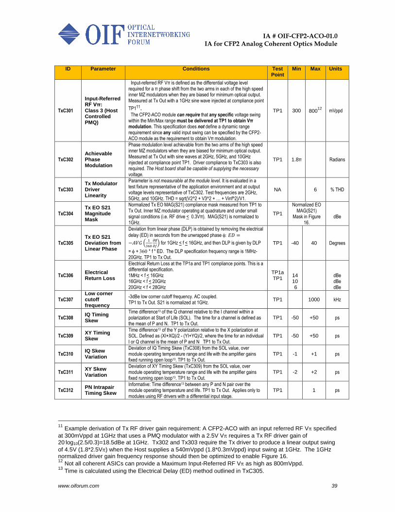
IA # OIF-CFP2-ACO-01.0
IA for CFP2 Analog Coherent Optics Module
www.oiforum.com 39
ID Parameter Conditions Test
Point Min Max Units
TxC301
Input-Referred RF Vπ: Class 3 (Host Controlled PMQ)
Input-referred RF Vπ is defined as the differential voltage level required for a π phase shift from the two arms in each of the high speed inner MZ modulators when they are biased for minimum optical output. Measured at Tx Out with a 1GHz sine wave injected at compliance point
TP111. The CFP2-ACO module can require that any specific voltage swing within the Min/Max range must be delivered at TP1 to obtain Vπ modulation. This specification does not define a dynamic range requirement since any valid input swing can be specified by the CFP2-ACO module as the requirement to obtain Vπ modulation.
TP1 300 80012
mVppd
TxC302 Achievable Phase Modulation
Phase modulation level achievable from the two arms of the high speed inner MZ modulators when they are biased for minimum optical output. Measured at Tx Out with sine waves at 2GHz, 5GHz, and 10GHz injected at compliance point TP1. Driver compliance to TxC303 is also required. The Host board shall be capable of supplying the necessary voltage.
TP1 1.8π Radians
TxC303 Tx Modulator Driver Linearity
Parameter is not measurable at the module level. It is evaluated in a test fixture representative of the application environment and at output voltage levels representative of TxC302. Test frequencies are 2GHz, 5GHz, and 10GHz. THD = sqrt(V2^2 + V3^2 + … + Vinf^2)/V1.
NA 6 % THD
TxC304 Tx EO S21 Magnitude Mask
Normalized Tx EO MAG(S21) compliance mask measured from TP1 to Tx Out. Inner MZ modulator operating at quadrature and under small signal conditions (i.e. RF drive < 0.3Vπ). MAG(S21) is normalized to 1GHz.
TP1
Normalized EO MAG(S21)
Mask in Figure 16.
dBe
TxC305 Tx EO S21 Deviation from Linear Phase
Deviation from linear phase (DLP) is obtained by removing the electrical
delay (ED) in seconds from the unwrapped phase 𝐸𝐷 =
−𝐴𝑉𝐺 (1
360
𝜕∅
𝜕𝑓) for 1GHz < f < 16GHz, and then DLP is given by DLP
= + *f * ED. The DLP specification frequency range is 1MHz-20GHz. TP1 to Tx Out.
TP1 -40 40 Degrees
TxC306 Electrical Return Loss
Electrical Return Loss at the TP1a and TP1 compliance points. This is a differential specification. 1MHz < f < 16GHz 16GHz < f < 20GHz 20GHz < f < 28GHz
TP1a TP1
14 10 6
dBe dBe dBe
TxC307 Low corner cutoff frequency
-3dBe low corner cutoff frequency. AC coupled. TP1 to Tx Out. S21 is normalized at 1GHz.
TP1 1000 kHz
TxC308 IQ Timing Skew
Time difference13 of the Q channel relative to the I channel within a polarization at Start of Life (SOL). The time for a channel is defined as the mean of P and N. TP1 to Tx Out.
TP1 -50 +50 ps
TxC309 XY Timing Skew
Time difference13 of the Y polarization relative to the X polarization at SOL. Defined as (XI+XQ)/2 - (YI+YQ)/2, where the time for an individual I or Q channel is the mean of P and N TP1 to Tx Out.
TP1 -50 +50 ps
TxC310 IQ Skew Variation
Deviation of IQ Timing Skew (TxC308) from the SOL value, over module operating temperature range and life with the amplifier gains fixed running open loop13. TP1 to Tx Out.
TP1 -1 +1 ps
TxC311 XY Skew Variation
Deviation of XY Timing Skew (TxC309) from the SOL value, over module operating temperature range and life with the amplifier gains fixed running open loop13. TP1 to Tx Out.
TP1 -2 +2 ps
TxC312 PN Intrapair Timing Skew
Informative: Time difference13 between any P and N pair over the module operating temperature and life. TP1 to Tx Out. Applies only to modules using RF drivers with a differential input stage.
TP1 1 ps
11
Example derivation of Tx RF driver gain requirement: A CFP2-ACO with an input referred RF V specified
at 300mVppd at 1GHz that uses a PMQ modulator with a 2.5V V requires a Tx RF driver gain of 20
.log10(2.5/0.3)=18.5dBe at 1GHz. Tx302 and Tx303 require the Tx driver to produce a linear output swing
of 4.5V (1.8*2.5V) when the Host supplies a 540mVppd (1.8*0.3mVppd) input swing at 1GHz. The 1GHz normalized driver gain frequency response should then be optimized to enable Figure 16. 12
Not all coherent ASICs can provide a Maximum Input-Referred RF V as high as 800mVppd. 13
Time is calculated using the Electrical Delay (ED) method outlined in TxC305.
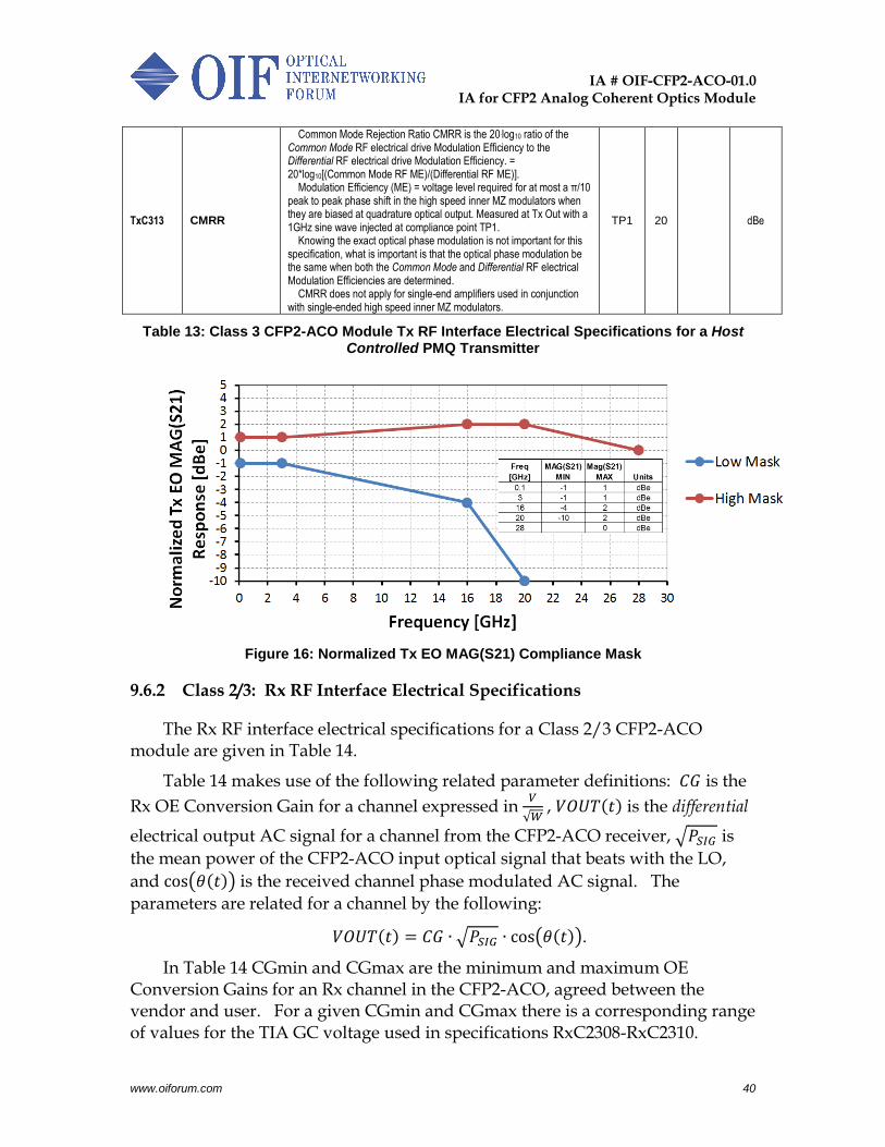
IA # OIF-CFP2-ACO-01.0
IA for CFP2 Analog Coherent Optics Module
www.oiforum.com 40
TxC313 CMRR
Common Mode Rejection Ratio CMRR is the 20.log10 ratio of the Common Mode RF electrical drive Modulation Efficiency to the Differential RF electrical drive Modulation Efficiency. = 20*log10[(Common Mode RF ME)/(Differential RF ME)]. Modulation Efficiency (ME) = voltage level required for at most a π/10 peak to peak phase shift in the high speed inner MZ modulators when they are biased at quadrature optical output. Measured at Tx Out with a 1GHz sine wave injected at compliance point TP1. Knowing the exact optical phase modulation is not important for this specification, what is important is that the optical phase modulation be the same when both the Common Mode and Differential RF electrical Modulation Efficiencies are determined. CMRR does not apply for single-end amplifiers used in conjunction with single-ended high speed inner MZ modulators.
TP1 20 dBe
Table 13: Class 3 CFP2-ACO Module Tx RF Interface Electrical Specifications for a Host Controlled PMQ Transmitter
Figure 16: Normalized Tx EO MAG(S21) Compliance Mask
9.6.2 Class 2/3: Rx RF Interface Electrical Specifications
The Rx RF interface electrical specifications for a Class 2/3 CFP2-ACO module are given in Table 14.
Table 14 makes use of the following related parameter definitions: 𝐶𝐺 is the
Rx OE Conversion Gain for a channel expressed in 𝑉
√𝑊 , 𝑉𝑂𝑈𝑇(𝑡) is the differential
electrical output AC signal for a channel from the CFP2-ACO receiver, √𝑃𝑆𝐼𝐺 is
the mean power of the CFP2-ACO input optical signal that beats with the LO,
and cos(𝜃(𝑡)) is the received channel phase modulated AC signal. The
parameters are related for a channel by the following:
𝑉𝑂𝑈𝑇(𝑡) = 𝐶𝐺 ∙ √𝑃𝑆𝐼𝐺 ∙ cos(𝜃(𝑡)).
In Table 14 CGmin and CGmax are the minimum and maximum OE Conversion Gains for an Rx channel in the CFP2-ACO, agreed between the vendor and user. For a given CGmin and CGmax there is a corresponding range of values for the TIA GC voltage used in specifications RxC2308-RxC2310.
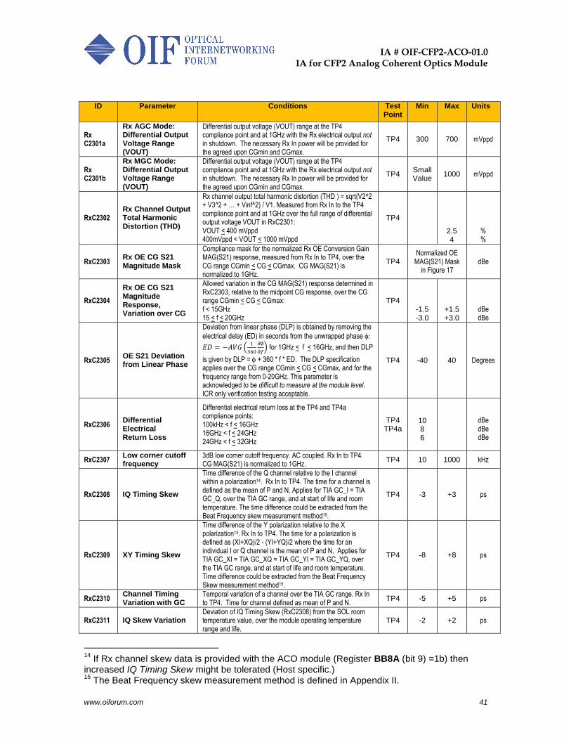
IA # OIF-CFP2-ACO-01.0
IA for CFP2 Analog Coherent Optics Module
www.oiforum.com 41
ID Parameter Conditions Test Point
Min Max Units
Rx C2301a
Rx AGC Mode: Differential Output Voltage Range (VOUT)
Differential output voltage (VOUT) range at the TP4 compliance point and at 1GHz with the Rx electrical output not in shutdown. The necessary Rx In power will be provided for the agreed upon CGmin and CGmax.
TP4 300 700 mVppd
Rx C2301b
Rx MGC Mode: Differential Output Voltage Range (VOUT)
Differential output voltage (VOUT) range at the TP4 compliance point and at 1GHz with the Rx electrical output not in shutdown. The necessary Rx In power will be provided for the agreed upon CGmin and CGmax.
TP4 Small Value
1000 mVppd
RxC2302 Rx Channel Output Total Harmonic Distortion (THD)
Rx channel output total harmonic distortion (THD ) = sqrt(V2^2 + V3^2 + … + Vinf^2) / V1. Measured from Rx In to the TP4 compliance point and at 1GHz over the full range of differential output voltage VOUT in RxC2301: VOUT < 400 mVppd 400mVppd < VOUT < 1000 mVppd
TP4
2.5 4
% %
RxC2303 Rx OE CG S21 Magnitude Mask
Compliance mask for the normalized Rx OE Conversion Gain MAG(S21) response, measured from Rx In to TP4, over the CG range CGmin < CG < CGmax. CG MAG(S21) is normalized to 1GHz.
TP4 Normalized OE
MAG(S21) Mask in Figure 17
dBe
RxC2304
Rx OE CG S21 Magnitude Response, Variation over CG
Allowed variation in the CG MAG(S21) response determined in RxC2303, relative to the midpoint CG response, over the CG range CGmin < CG < CGmax: f < 15GHz 15 < f < 20GHz
TP4
-1.5 -3.0
+1.5 +3.0
dBe dBe
RxC2305 OE S21 Deviation from Linear Phase
Deviation from linear phase (DLP) is obtained by removing the
electrical delay (ED) in seconds from the unwrapped phase
𝐸𝐷 = −𝐴𝑉𝐺 (1
360
𝜕∅
𝜕𝑓)for 1GHz < f < 16GHz, and then DLP
is given by DLP = + 360 * f * ED. The DLP specification applies over the CG range CGmin < CG < CGmax, and for the frequency range from 0-20GHz. This parameter is acknowledged to be difficult to measure at the module level. ICR only verification testing acceptable.
TP4 -40 40 Degrees
RxC2306
Differential Electrical Return Loss
Differential electrical return loss at the TP4 and TP4a compliance points: 100kHz < f < 16GHz 16GHz < f < 24GHz 24GHz < f < 32GHz
TP4 TP4a
10 8 6
dBe dBe dBe
RxC2307 Low corner cutoff frequency
3dB low corner cutoff frequency. AC coupled. Rx In to TP4. CG MAG(S21) is normalized to 1GHz.
TP4 10 1000 kHz
RxC2308 IQ Timing Skew
Time difference of the Q channel relative to the I channel within a polarization14. Rx In to TP4. The time for a channel is defined as the mean of P and N. Applies for TIA GC_I = TIA GC_Q, over the TIA GC range, and at start of life and room temperature. The time difference could be extracted from the Beat Frequency skew measurement method15.
TP4 -3 +3 ps
RxC2309 XY Timing Skew
Time difference of the Y polarization relative to the X polarization14. Rx In to TP4. The time for a polarization is defined as (XI+XQ)/2 - (YI+YQ)/2 where the time for an individual I or Q channel is the mean of P and N. Applies for TIA GC_XI = TIA GC_XQ = TIA GC_YI = TIA GC_YQ, over the TIA GC range, and at start of life and room temperature. Time difference could be extracted from the Beat Frequency Skew measurement method15.
TP4 -8 +8 ps
RxC2310 Channel Timing Variation with GC
Temporal variation of a channel over the TIA GC range. Rx In to TP4. Time for channel defined as mean of P and N.
TP4 -5 +5 ps
RxC2311 IQ Skew Variation Deviation of IQ Timing Skew (RxC2308) from the SOL room temperature value, over the module operating temperature range and life.
TP4 -2 +2 ps
14
If Rx channel skew data is provided with the ACO module (Register BB8A (bit 9) =1b) then increased IQ Timing Skew might be tolerated (Host specific.) 15
The Beat Frequency skew measurement method is defined in Appendix II.
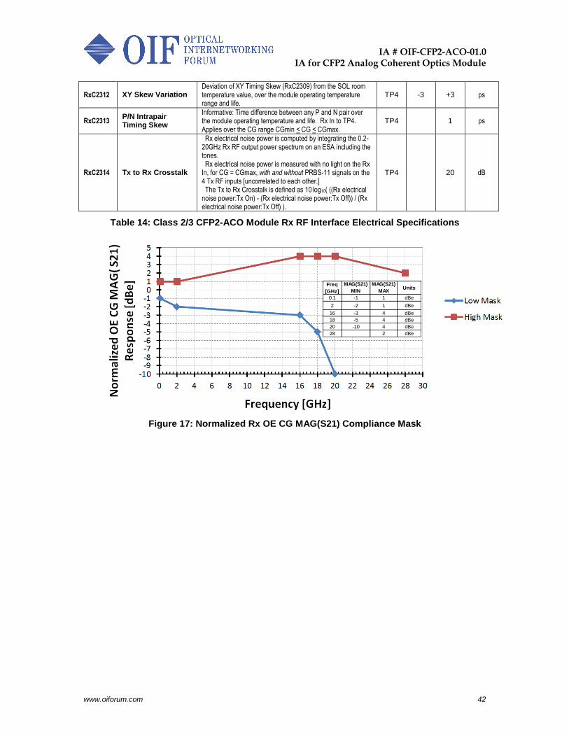
IA # OIF-CFP2-ACO-01.0
IA for CFP2 Analog Coherent Optics Module
www.oiforum.com 42
RxC2312 XY Skew Variation Deviation of XY Timing Skew (RxC2309) from the SOL room temperature value, over the module operating temperature range and life.
TP4 -3 +3 ps
RxC2313 P/N Intrapair Timing Skew
Informative: Time difference between any P and N pair over the module operating temperature and life. Rx In to TP4. Applies over the CG range CGmin < CG < CGmax.
TP4
1 ps
RxC2314 Tx to Rx Crosstalk
Rx electrical noise power is computed by integrating the 0.2-20GHz Rx RF output power spectrum on an ESA including the tones. Rx electrical noise power is measured with no light on the Rx In, for CG = CGmax, with and without PRBS-11 signals on the 4 Tx RF inputs [uncorrelated to each other.] The Tx to Rx Crosstalk is defined as 10.log10( ((Rx electrical noise power:Tx On) - (Rx electrical noise power:Tx Off)) / (Rx electrical noise power:Tx Off) ).
TP4 20 dB
Table 14: Class 2/3 CFP2-ACO Module Rx RF Interface Electrical Specifications
Figure 17: Normalized Rx OE CG MAG(S21) Compliance Mask
Freq
[GHz]
MAG(S21)
MIN
MAG(S21)
MAXUnits
0.1 -1 1 dBe
2 -2 1 dBe
16 -3 4 dBe
18 -5 4 dBe
20 -10 4 dBe
28 2 dBe
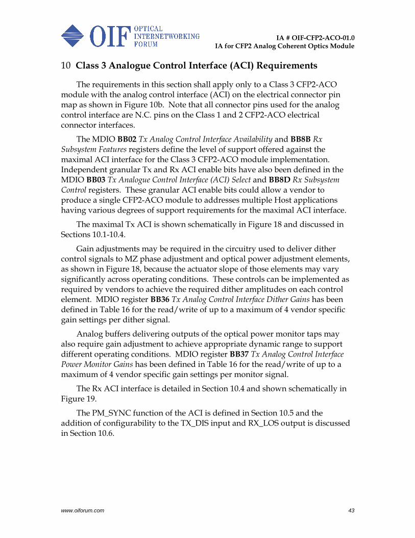
IA # OIF-CFP2-ACO-01.0
IA for CFP2 Analog Coherent Optics Module
www.oiforum.com 43
Class 3 Analogue Control Interface (ACI) Requirements 10
The requirements in this section shall apply only to a Class 3 CFP2-ACO module with the analog control interface (ACI) on the electrical connector pin map as shown in Figure 10b. Note that all connector pins used for the analog control interface are N.C. pins on the Class 1 and 2 CFP2-ACO electrical connector interfaces.
The MDIO BB02 Tx Analog Control Interface Availability and BB8B Rx Subsystem Features registers define the level of support offered against the maximal ACI interface for the Class 3 CFP2-ACO module implementation. Independent granular Tx and Rx ACI enable bits have also been defined in the MDIO BB03 Tx Analogue Control Interface (ACI) Select and BB8D Rx Subsystem Control registers. These granular ACI enable bits could allow a vendor to produce a single CFP2-ACO module to addresses multiple Host applications having various degrees of support requirements for the maximal ACI interface.
The maximal Tx ACI is shown schematically in Figure 18 and discussed in Sections 10.1-10.4.
Gain adjustments may be required in the circuitry used to deliver dither control signals to MZ phase adjustment and optical power adjustment elements, as shown in Figure 18, because the actuator slope of those elements may vary significantly across operating conditions. These controls can be implemented as required by vendors to achieve the required dither amplitudes on each control element. MDIO register BB36 Tx Analog Control Interface Dither Gains has been defined in Table 16 for the read/write of up to a maximum of 4 vendor specific gain settings per dither signal.
Analog buffers delivering outputs of the optical power monitor taps may also require gain adjustment to achieve appropriate dynamic range to support different operating conditions. MDIO register BB37 Tx Analog Control Interface Power Monitor Gains has been defined in Table 16 for the read/write of up to a maximum of 4 vendor specific gain settings per monitor signal.
The Rx ACI interface is detailed in Section 10.4 and shown schematically in Figure 19.
The PM_SYNC function of the ACI is defined in Section 10.5 and the addition of configurability to the TX_DIS input and RX_LOS output is discussed in Section 10.6.
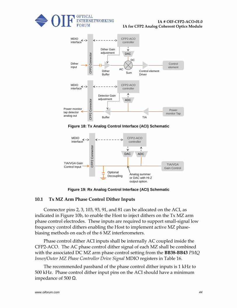
IA # OIF-CFP2-ACO-01.0
IA for CFP2 Analog Coherent Optics Module
www.oiforum.com 44
Figure 18: Tx Analog Control Interface (ACI) Schematic
Figure 19: Rx Analog Control Interface (ACI) Schematic
10.1 Tx MZ Arm Phase Control Dither Inputs
Connector pins 2, 3, 103, 93, 91, and 81 can be allocated on the ACI, as indicated in Figure 10b, to enable the Host to inject dithers on the Tx MZ arm phase control electrodes. These inputs are required to support small-signal low frequency control dithers enabling the Host to implement active MZ phase-biasing methods on each of the 6 MZ interferometers.
Phase control dither ACI inputs shall be internally AC coupled inside the CFP2-ACO. The AC phase control dither signal of each MZ shall be combined with the associated DC MZ arm phase control setting from the BB38-BB43 PMQ Inner/Outer MZ Phase Controller Drive Signal MDIO registers in Table 16.
The recommended passband of the phase control dither inputs is 1 kHz to 500 kHz. Phase control dither input pins on the ACI should have a minimum impedance of 500 Ω.
DAC
Dither
BufferSum
DC
AC
CF
P2
Con
ne
cto
r
Control element
Driver
Control
element
Dither
input
CFP2-ACO
controller
MDIO
interface
Dither Gain
adjustment
ADC
Buffer
CF
P2
Con
ne
cto
r
TIA
Power
monitor Tap
Power monitor
tap detector
analog out
CFP2-ACO
controller
MDIO
interface
Detector Gain
adjustment
DAC
Optional
Decoupling
TIA/VGA
Gain Control
TIA/VGA Gain
Control Input
CFP2-ACO
controller
MDIO
interface
CF
P2
Co
nn
ecto
r
ADC
Analog summer
or DAC with Hi-Z
output option.
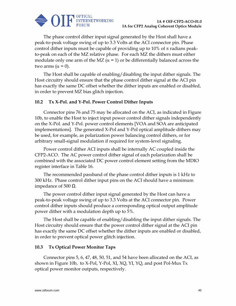
IA # OIF-CFP2-ACO-01.0
IA for CFP2 Analog Coherent Optics Module
www.oiforum.com 45
The phase control dither input signal generated by the Host shall have a peak-to-peak voltage swing of up to 3.3 Volts at the ACI connector pin. Phase
control dither inputs must be capable of providing up to 10% of radians peak-to-peak on each of the MZ relative phase. For each MZ the dithers must either
modulate only one arm of the MZ ( = 1) or be differentially balanced across the
two arms ( = 0).
The Host shall be capable of enabling/disabling the input dither signals. The Host circuitry should ensure that the phase control dither signal at the ACI pin has exactly the same DC offset whether the dither inputs are enabled or disabled, in order to prevent MZ bias glitch injection.
10.2 Tx X-Pol. and Y-Pol. Power Control Dither Inputs
Connector pins 76 and 75 may be allocated on the ACI, as indicated in Figure 10b, to enable the Host to inject input power control dither signals independently on the X-Pol. and Y-Pol. power control elements [VOA and SOA are anticipated implementations]. The generated X-Pol and Y-Pol optical amplitude dithers may be used, for example, as polarization power balancing control dithers, or for arbitrary small-signal modulation if required for system-level signaling.
Power control dither ACI inputs shall be internally AC coupled inside the CFP2-ACO. The AC power control dither signal of each polarization shall be combined with the associated DC power control element setting from the MDIO register interface in Table 16.
The recommended passband of the phase control dither inputs is 1 kHz to 300 kHz. Phase control dither input pins on the ACI should have a minimum impedance of 500 Ω.
The power control dither input signal generated by the Host can have a peak-to-peak voltage swing of up to 3.3 Volts at the ACI connector pin. Power control dither inputs should produce a corresponding optical output amplitude power dither with a modulation depth up to 5%.
The Host shall be capable of enabling/disabling the input dither signals. The Host circuitry should ensure that the power control dither signal at the ACI pin has exactly the same DC offset whether the dither inputs are enabled or disabled, in order to prevent optical power glitch injection.
10.3 Tx Optical Power Monitor Taps
Connector pins 5, 6, 47, 48, 50, 51, and 54 have been allocated on the ACI, as shown in Figure 10b, to X-Pol, Y-Pol, XI, XQ, YI, YQ, and post Pol-Mux Tx optical power monitor outputs, respectively.
IA # OIF-CFP2-ACO-01.0
IA for CFP2 Analog Coherent Optics Module
www.oiforum.com 46
Available optical power monitor outputs are to be used to detect the outcomes of control dither inputs described in Sections 10.1-10.2, thereby providing feedback to the associated control loops. Each available optical power monitor tap must be provided to the connector using a TIA element with appropriate gain and bandwidth to support detection of control dither outcomes.
The Tx optical power monitor tap output signals at the ACI connector are DC-coupled, with a peak-to-peak voltage between 0.0 and 3.3 Volts. They may be used by the Host to detect both DC and AC signals so the monitor signals have a recommended passband from DC to 500 kHz. The optical power monitor ACI outputs should be capable of driving a Host board with a minimum 1 kΩ load and a maximum of 1 nF input capacitance.
10.4 Rx TIA/VGA Gain Control Inputs
Connector pins 63, 64, 66, and 67 have been allocated on the ACI, as indicated in Figure 10b, to enable the Host to directly control the TIA/VGA transimpedance Gain Control (GC) on all 4 Rx RF channels. The Host shall be capable of enabling/disabling the GC ACI inputs (i.e. High-Z option).
The GC input operating range shall be confined to a subset of 0 to 3.3 V. The absolute min/max voltage on the GC input shall be allowed between -0.5 V and 4 V. The ACI GC connector input bandwidth shall be >1 MHz. Decoupling capacitance to ground on the GC connections inside the CFP2-ACO is optional.
If a vendor choses to do so, it is feasible to have the TIA/VGA GC input driven from two sources as shown in Figure 19. Anticipated implementations include an internal GC DAC with a Hi-Z option or an analog summer circuit to prevent signal contention. In this scenario enabling the Rx ACI bit (bit 8) and
setting the TIA into MGC mode (bit 15-14) using the MDIO BB8D Rx Subsystem Control register shall activate the GC ACI inputs. The ADC is present on the GC line in Figure 19 to allow the controller to read the GC value if the TIA/VGA is operating in an AGC mode.
10.5 PM_SYNC Input
For the CFP2-ACO module the PRG_CNTL2 has been allocated for an external Performance Monitoring Synchronization input (PM_SYNC.) This input enables a rising edge synchronization pulse from the Host time reference source to synchronize the CFP2-ACO performance monitoring data collection with the Host data collection.
The CFP2-ACO PM_SYNC input shall share requirements with, and operate equivalently to, the PM_SYNC input on pin B13 in the Ref. [5] OIF-MSA-100GLH-EM-01.1 IA. The PM_SYNC function is detailed in Section 8.4.1.4, Table
IA # OIF-CFP2-ACO-01.0
IA for CFP2 Analog Coherent Optics Module
www.oiforum.com 47
4 and Table 9 of Ref. [5], and in Section 6.2.5 of Ref. [2]. The LVCMOS input has a default period=1 second; min high/low time = 100msec.
10.6 TX_DIS Input and RX_LOS Output Configurability
TX_DIS on connector pin 24 of the ACI can be optionally configurable as a PRG_CNTL (programmable control) after Reset. This functionality is equivalent to that introduced on the CFP4 pin map in Ref. [4].
RX_LOS on connector pin 25 of the ACI can be optionally configurable as a PRG_ALRM (programmable alarm) after Reset. This functionality is equivalent to that introduced on the CFP4 pin map in Ref. [4].
IA # OIF-CFP2-ACO-01.0
IA for CFP2 Analog Coherent Optics Module
www.oiforum.com 48
MDIO Register Interface 11
11.1 Implementation Overview
The CFP2 module utilizes MDIO IEEE Std. 802.3TM-2012 clause 45 [8] for its management interface. The CFP2 MDIO implementation is defined in Ref. [2], “CFP MSA Management Interface Specification.” When multiple CFP2 modules are connected via a single bus, a particular CFP2 module can be selected by using the Physical Port Address pins.
An overview of the 0xB000 register page allocations that were added previously in the CFP MSA MIS to support the OIF MSA-100GLH coherent module application are given in Table 36 of Ref. [2].
To enable support of the CFP2-ACO module, informative Section 12 specifies new Ref. [2] 0xB000 register page extensions and Ref. [2] content modifications. Section 12 has been liaised to the CFP MSA Spokesperson and the CFP MSA Technical Editor for inclusion in the future CFP MSA MIS V2.6 release following the CFP MSA review process. These extensions and modifications further re-enforce a common Host-module management interface implementation for both high-speed client and line-side optical transmission module applications.
The CFP2-ACO shall utilize the expanded 0xB000 register page definition in the upcoming V2.6 of the CFP MSA MIS. Revision authority and document control for the CFP2-ACO MDIO interface resides with the CFP MSA MIS Editor. Any and all revisions to the normative Ref. [2] “CFP MSA Management Interface Specification” shall take precedence over the informative content in Section 12 and Section 13 of this IA. The current normative MIS reference for implementing the CFP2-ACO MDIO interface can be found at the Ref. [1] CFP MSA webpage.
The CFP MSA MIS Section 6.2.3 [2] specifies MDIO write flow control for the 0xB000 register page. Note that writing to unimplemented registers shall have no effect and shall not raise any errors, i.e. B050 bit 14 shall return 0: No Error.
The CFP2-ACO module shall have the capability to use a Performance Monitor Tick, as detailed in the Performance Monitoring Subsystem Section 6.2.5.1 of Ref [2]. This PM Tick can be generated internally or be provided by the Host through a PM_SYNC input on PRG_CNTL2.16 For performance monitored variables, in addition to the current value, the Host has access to average, minimum, and maximum values over the PM Tick interval.
16
The Host is free to reprogram the usage of the PRG_CNTLn input pins and change their values at any time after the module exits the Initialize State.
IA # OIF-CFP2-ACO-01.0
IA for CFP2 Analog Coherent Optics Module
www.oiforum.com 49
For clarity CFP2-ACO relevant 0xB000 registers in CFP MSA MIS V2.4 R06b have been collected in informative Sections 13.1-13.6.
The existing 0xB000 tunable source control and performance monitoring registers are reproduced for reference in Section 13.1-13.2, and they shall be used for the CFP2-ACO module application.
11.2 CFP2-ACO Calibration Data
It is anticipated that CFP2-ACO module calibration data, subject to agreement between CFP2-ACO module users and vendors, could be stored in the existing CFP MSA MIS vendor specific registers:
Unused registers in the range BAE0 – BAFF shall be requested from the register fields allocated for MSA-100GLH Network Lane VR2 to be used to store the ACO module calibration data defined in Section 12.7.
Read-Only Vendor Non-Volatile Registers (NVR) are available between 8400-847F [Vendor NVR 1: 1 Table=128 registers, 8-bit] and 8480-84FF [Vendor NVR 2: 1 Table=128 registers, 8-bit.]
The OIF shall request from the MIS Editor that two additional Tables of Read-Only Vendor Non-Volatile Registers (NVR) be provided from the MSA Reserved space between 8500-87FF.
A Read-Only page [9000-9FFF] of registers [4096] is reserved for vendor private use. This space is reserved exclusively for module vendors’ development and implementation needs; it is assumed however that, subject to agreement between a CFP2-ACO module user and vendor, a subset of this space can be made non-volatile to contain additional calibration data.
11.3 CFP2-ACO User Private Use Registers
It is anticipated that CFP2-ACO module users will require private use registers. The existing CFP MSA MIS user registers shall be used for this purpose:
Read/Write User Non-Volatile Registers (NVR) are available between 8800-887F [User NVR 1: 1 table=128 registers, 8-bit] and 8880-88FF [User NVR 2: 1 table=128 registers, 8-bit.]
The OIF shall request from the MIS Editor that two additional 16-bit Tables of Read/Write User Non-Volatile Registers (NVR) be provided from the MSA Reserved space between 8900-8EFF.
Starting at 8F00h, two additional tables [2x128 registers] are allocated for “User private use”. The CFP MSA MIS does not specify nor restrict
IA # OIF-CFP2-ACO-01.0
IA for CFP2 Analog Coherent Optics Module
www.oiforum.com 50
the use of these tables; however, the use of these User Private Use Registers is subject to additional agreement between CFP2-ACO module users and vendors. It is assumed that these registers can be defined as non-volatile as part of any such additional agreement.
OIF Requested CFP MSA MIS V2.4 R06b Extensions and 12Modifications Supporting the CFP2-ACO Module (Informative)
The OIF requested changes to existing CFP MSA MIS V2.4 R06b content is given in Section 12.1.
The two MSA reserved tables between BB00-BBFF shall be requested for the new CFP2-ACO module specific Tx and Rx registers given in Section 12.2-12.3. MSA reserved registers between BAE0-BAFF shall also be requested for the ACO module characteristic data provided in Section 12.7. Note however, the final authority for allocation resides with the CFP MSA MIS Editor.
New CFP2-ACO FAWS registers are provided in Section 12.4.
The CFP2-ACO wavelength change operation is outlined in Section 12.5.
The CFP2-ACO wavelength selection registers are discussed in Section 12.6.
The CFP2-ACO characteristic data registers are provided in Section 12.7.
12.1 OIF Requested Changes to Existing CFP MSA MIS V2.4 R06b Content
The OIF shall request that Chapter 6 in CFP MSA MIS be renamed from “MSA-100GLH Module Management Interface” to “Coherent Module Management Interface”. This emphasizes commonality in the registers used for coherent technology across various optical module types.
The OIF shall request from the MIS Editor that two additional Tables of Read-Only Vendor Non-Volatile Registers (NVR) be provided from the MSA Reserved space between 8500-87FF.
The OIF shall request from the MIS Editor that two additional 16-bit Tables of Read/Write User Non-Volatile Registers (NVR) be provided from the MSA Reserved space between 8900-8EFF.
When the LO source is shared with the Tx source, i.e. BB8B Rx Subsystem Features register bit 10:9=00, the Rx laser source registers in the 0xB000 register set are not supported, and should behave like unimplemented registers in the CFP MSA MIS for consistency.
The OIF shall request from the MIS Editor that Section 6.2.2.2 (page 111) lines 7-8 in Ref. [2] clarify the different use cases for the fine tune frequency registers. The B430 and B440 Fine Tune Frequency registers shall be available in the CFP2-ACO (they are not optional.) When the B430 and B440 Fine Tune
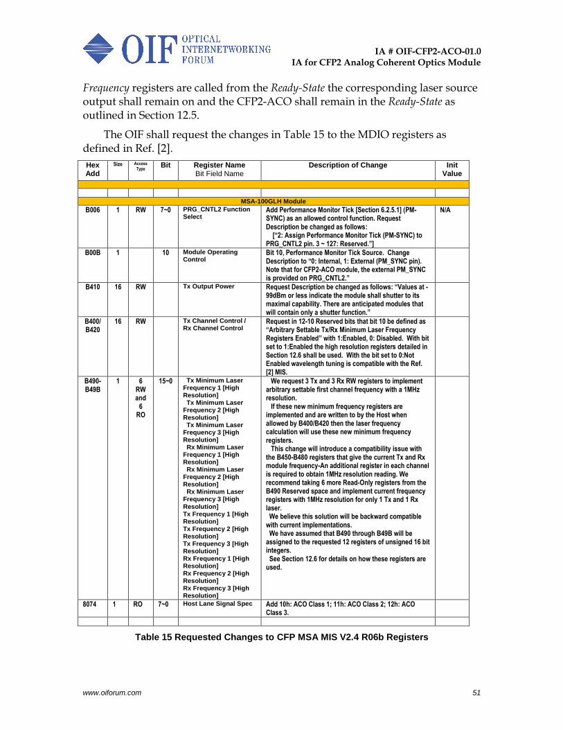
IA # OIF-CFP2-ACO-01.0
IA for CFP2 Analog Coherent Optics Module
www.oiforum.com 51
Frequency registers are called from the Ready-State the corresponding laser source output shall remain on and the CFP2-ACO shall remain in the Ready-State as outlined in Section 12.5.
The OIF shall request the changes in Table 15 to the MDIO registers as defined in Ref. [2].
Hex Add
Size Access Type
Bit Register Name Bit Field Name
Description of Change Init Value
MSA-100GLH Module
B006 1 RW 7~0 PRG_CNTL2 Function Select
Add Performance Monitor Tick [Section 6.2.5.1] (PM-SYNC) as an allowed control function. Request Description be changed as follows: [“2: Assign Performance Monitor Tick (PM-SYNC) to PRG_CNTL2 pin. 3 ~ 127: Reserved.”]
N/A
B00B 1 10 Module Operating Control
Bit 10, Performance Monitor Tick Source. Change Description to “0: Internal, 1: External (PM_SYNC pin). Note that for CFP2-ACO module, the external PM_SYNC is provided on PRG_CNTL2.”
B410 16 RW Tx Output Power Request Description be changed as follows: “Values at -99dBm or less indicate the module shall shutter to its maximal capability. There are anticipated modules that will contain only a shutter function.”
B400/B420
16 RW Tx Channel Control / Rx Channel Control
Request in 12-10 Reserved bits that bit 10 be defined as “Arbitrary Settable Tx/Rx Minimum Laser Frequency Registers Enabled” with 1:Enabled, 0: Disabled. With bit set to 1:Enabled the high resolution registers detailed in Section 12.6 shall be used. With the bit set to 0:Not Enabled wavelength tuning is compatible with the Ref. [2] MIS.
B490- B49B
1 6 RW and
6 RO
15~0 Tx Minimum Laser Frequency 1 [High Resolution] Tx Minimum Laser Frequency 2 [High Resolution] Tx Minimum Laser Frequency 3 [High Resolution] Rx Minimum Laser Frequency 1 [High Resolution] Rx Minimum Laser Frequency 2 [High Resolution] Rx Minimum Laser Frequency 3 [High Resolution] Tx Frequency 1 [High Resolution] Tx Frequency 2 [High Resolution] Tx Frequency 3 [High Resolution] Rx Frequency 1 [High Resolution] Rx Frequency 2 [High Resolution] Rx Frequency 3 [High Resolution]
We request 3 Tx and 3 Rx RW registers to implement arbitrary settable first channel frequency with a 1MHz resolution. If these new minimum frequency registers are implemented and are written to by the Host when allowed by B400/B420 then the laser frequency calculation will use these new minimum frequency registers. This change will introduce a compatibility issue with the B450-B480 registers that give the current Tx and Rx module frequency-An additional register in each channel is required to obtain 1MHz resolution reading. We recommend taking 6 more Read-Only registers from the B490 Reserved space and implement current frequency registers with 1MHz resolution for only 1 Tx and 1 Rx laser. We believe this solution will be backward compatible with current implementations. We have assumed that B490 through B49B will be assigned to the requested 12 registers of unsigned 16 bit integers. See Section 12.6 for details on how these registers are used.
8074 1 RO 7~0 Host Lane Signal Spec Add 10h: ACO Class 1; 11h: ACO Class 2; 12h: ACO Class 3.
Table 15 Requested Changes to CFP MSA MIS V2.4 R06b Registers
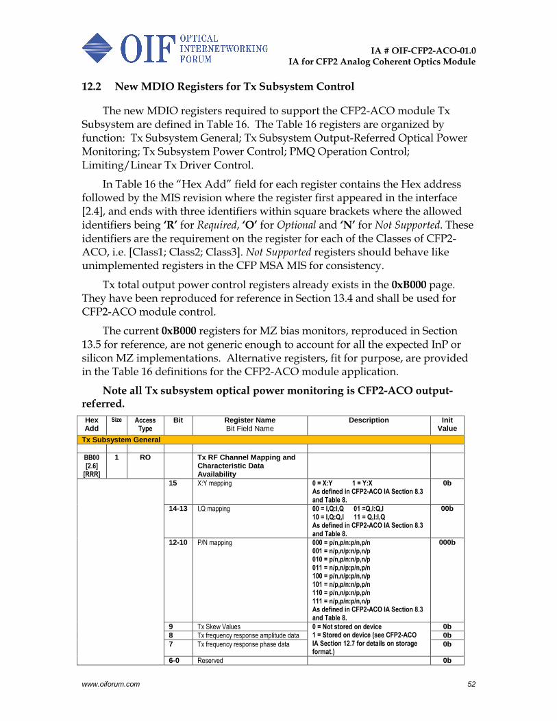
IA # OIF-CFP2-ACO-01.0
IA for CFP2 Analog Coherent Optics Module
www.oiforum.com 52
12.2 New MDIO Registers for Tx Subsystem Control
The new MDIO registers required to support the CFP2-ACO module Tx Subsystem are defined in Table 16. The Table 16 registers are organized by function: Tx Subsystem General; Tx Subsystem Output-Referred Optical Power Monitoring; Tx Subsystem Power Control; PMQ Operation Control; Limiting/Linear Tx Driver Control.
In Table 16 the “Hex Add” field for each register contains the Hex address followed by the MIS revision where the register first appeared in the interface [2.4], and ends with three identifiers within square brackets where the allowed identifiers being ‘R’ for Required, ‘O’ for Optional and ‘N’ for Not Supported. These identifiers are the requirement on the register for each of the Classes of CFP2-ACO, i.e. [Class1; Class2; Class3]. Not Supported registers should behave like unimplemented registers in the CFP MSA MIS for consistency.
Tx total output power control registers already exists in the 0xB000 page. They have been reproduced for reference in Section 13.4 and shall be used for CFP2-ACO module control.
The current 0xB000 registers for MZ bias monitors, reproduced in Section 13.5 for reference, are not generic enough to account for all the expected InP or silicon MZ implementations. Alternative registers, fit for purpose, are provided in the Table 16 definitions for the CFP2-ACO module application.
Note all Tx subsystem optical power monitoring is CFP2-ACO output-referred.
Hex Add
Size Access Type
Bit Register Name Bit Field Name
Description Init Value
Tx Subsystem General
BB00 [2.6]
[RRR]
1 RO Tx RF Channel Mapping and Characteristic Data Availability
15 X:Y mapping 0 = X:Y 1 = Y:X As defined in CFP2-ACO IA Section 8.3 and Table 8.
0b
14-13 I,Q mapping 00 = I,Q:I,Q 01 =Q,I:Q,I 10 = I,Q:Q,I 11 = Q,I:I,Q As defined in CFP2-ACO IA Section 8.3 and Table 8.
00b
12-10 P/N mapping 000 = p/n,p/n:p/n,p/n 001 = n/p,n/p:n/p,n/p 010 = p/n,p/n:n/p,n/p 011 = n/p,n/p:p/n,p/n 100 = p/n,n/p:p/n,n/p 101 = n/p,p/n:n/p,p/n 110 = p/n,n/p:n/p,p/n 111 = n/p,p/n:p/n,n/p As defined in CFP2-ACO IA Section 8.3 and Table 8.
000b
9 Tx Skew Values 0 = Not stored on device 1 = Stored on device (see CFP2-ACO IA Section 12.7 for details on storage format.)
0b
8 Tx frequency response amplitude data 0b
7 Tx frequency response phase data 0b
6-0 Reserved 0b
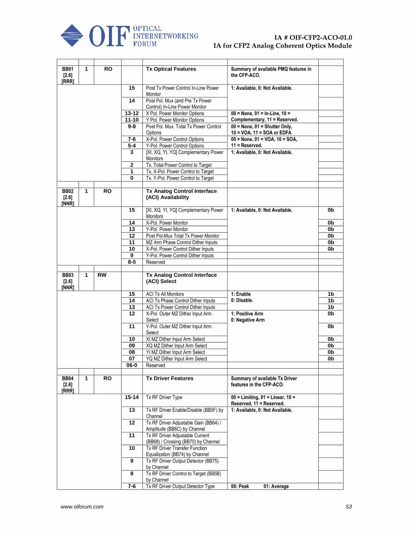
IA # OIF-CFP2-ACO-01.0
IA for CFP2 Analog Coherent Optics Module
www.oiforum.com 53
BB01 [2.6]
[RRR]
1 RO Tx Optical Features Summary of available PMQ features in the CFP-ACO.
15 Post Tx Power Control In-Line Power Monitor
1: Available, 0: Not Available.
14 Post Pol. Mux (and Pre Tx Power Control) In-Line Power Monitor
13-12 X Pol. Power Monitor Options 00 = None, 01 = In-Line, 10 = Complementary, 11 = Reserved.
11-10 Y Pol. Power Monitor Options
9-8 Post Pol. Mux. Total Tx Power Control Options
00 = None, 01 = Shutter Only, 10 = VOA, 11 = SOA or EDFA
7-6 X-Pol. Power Control Options 00 = None, 01 = VOA, 10 = SOA, 11 = Reserved.
5-4 Y-Pol. Power Control Options
3 [XI, XQ, YI, YQ] Complementary Power Monitors
1: Available, 0: Not Available.
2 Tx. Total Power Control to Target
1 Tx. X-Pol. Power Control to Target
0 Tx. Y-Pol. Power Control to Target
BB02 [2.6]
[NNR]
1 RO Tx Analog Control Interface (ACI) Availability
15 [XI, XQ, YI, YQ] Complementary Power Monitors
1: Available, 0: Not Available. 0b
14 X-Pol. Power Monitor 0b
13 Y-Pol. Power Monitor 0b
12 Post Pol-Mux Total Tx Power Monitor 0b
11 MZ Arm Phase Control Dither Inputs 0b
10 X-Pol. Power Control Dither Inputs 0b
9 Y-Pol. Power Control Dither Inputs
8-0 Reserved
BB03 [2.6]
[NNR]
1 RW Tx Analog Control Interface (ACI) Select
15 ACI Tx All Monitors 1: Enable 0: Disable.
1b
14 ACI Tx Phase Control Dither Inputs 1b
13 ACI Tx Power Control Dither Inputs 1b
12 X-Pol. Outer MZ Dither Input Arm Select
1: Positive Arm 0: Negative Arm
0b
11 Y-Pol. Outer MZ Dither Input Arm Select
0b
10 XI MZ Dither Input Arm Select 0b
09 XQ MZ Dither Input Arm Select 0b
08 YI MZ Dither Input Arm Select 0b
07 YQ MZ Dither Input Arm Select 0b
06-0 Reserved
BB04 [2.6]
[RRR]
1 RO Tx Driver Features Summary of available Tx Driver features in the CFP-ACO.
15-14 Tx RF Driver Type 00 = Limiting, 01 = Linear, 10 = Reserved, 11 = Reserved.
13 Tx RF Driver Enable/Disable (BB5F) by Channel
1: Available, 0: Not Available.
12 Tx RF Driver Adjustable Gain (BB64) / Amplitude (BB6C) by Channel
11 Tx RF Driver Adjustable Current (BB68) / Crossing (BB70) by Channel
10 Tx RF Driver Transfer Function Equalization (BB74) by Channel
9 Tx RF Driver Output Detector (BB75) by Channel
8 Tx RF Driver Control to Target (BB5B) by Channel
7-6 Tx RF Driver Output Detector Type 00: Peak 01: Average
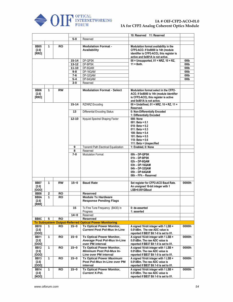
IA # OIF-CFP2-ACO-01.0
IA for CFP2 Analog Coherent Optics Module
www.oiforum.com 54
10: Reserved 11: Reserved
5-0 Reserved
BB05 [2.6]
[RRO]
1 RO Modulation Format - Availability
Modulation format availability in the CFP2-ACO. If 0x8000 is 14h (module identifier is CFP2-ACO), this register is active and 0x801A is not active.
15-14 DP-QPSK 00 = Unsupported, 01 = NRZ, 10 = RZ, 11 = Both.
00b
13-12 DP-BPSK 00b
11-10 DP-8QAM 00b
9-8 DP-16QAM 00b
7-6 DP-32QAM 00b
5-4 DP-64QAM 00b
3-0 Reserved
BB06 [2.6]
[RRO]
1 RW Modulation Format - Select Modulation format select in the CFP2-ACO. If 0x8000 is 14h (module identifier is CFP2-ACO), this register is active and 0x801A is not active.
15-14 RZ/NRZ Encoding 00 = Undefined, 01 = NRZ, 10 = RZ, 11 = Reserved.
13 Differential Encoding Status 0: Non-Differentially Encoded 1: Differentially Encoded
12-10 Nyquist Spectral Shaping Factor 000: None 001: Beta = 0.1 010: Beta = 0.2 011: Beta = 0.3 100: Beta = 0.4 101: Beta = 0.5 110: Beta = 0.6 111: Beta = Unspecified
9 Transmit Path Electrical Equalization 1: Enabled, 0: None
8 Reserved
7-0 Modulation Format 00h – DP-QPSK 01h – DP-BPSK 02h – DP-8QAM 03h – DP-16QAM 04h – DP-32QAM 05h – DP-64QAM 06h – FFh – Reserved
BB07 [2.6]
[OOO]
1 RW 15~0 Baud Rate Set register for CFP2-ACO Baud Rate. An unsigned 16-bit integer with 1 LSB=0.001GBaud
0000h
BB08 2 RO Reserved
BB0A [2.6]
[RRR]
1 RO Module Tx Hardware Response Pending Flags
15 Tx Fine Tune Frequency (B430) In Progress
0: de-asserted 1: asserted
14~0 Reserved
BB0C 5 RO Reserved
Tx Subsystem Output-Referred Optical Power Monitoring
BB10 [2.6]
[OOO]
1 RO 15~0 Tx Optical Power Monitor, Current Post Pol-Mux In-Line
A signed 16-bit integer with 1 LSB = 0.01dBm. The raw ADC value is reported if BB37 Bit 1-0 is set to 01.
0000h
BB11 [2.6]
[OOO]
1 RO 15~0 Tx Optical Power Monitor, Average Post Pol-Mux In-Line over PM interval
A signed 16-bit integer with 1 LSB = 0.01dBm. The raw ADC value is reported if BB37 Bit 1-0 is set to 01.
0000h
BB12 [2.6]
[OOO]
1 RO 15~0 Tx Optical Power Monitor, Minimum Post Pol-Mux In-Line over PM interval
A signed 16-bit integer with 1 LSB = 0.01dBm. The raw ADC value is reported if BB37 Bit 1-0 is set to 01.
0000h
BB13 [2.6]
[OOO]
1 RO 15~0 Tx Optical Power Maximum Post Pol-Mux In-Line over PM interval
A signed 16-bit integer with 1 LSB = 0.01dBm. The raw ADC value is reported if BB37 Bit 1-0 is set to 01.
0000h
BB14 [2.6]
[NOO]
1 RO 15~0 Tx Optical Power Monitor, Current X-Pol.
A signed 16-bit integer with 1 LSB = 0.01dBm. The raw ADC value is reported if BB37 Bit 1-0 is set to 01.
0000h
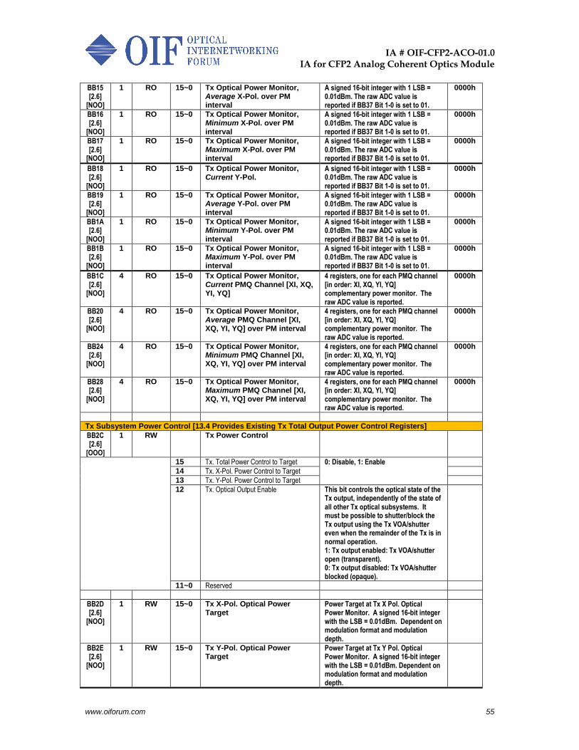
IA # OIF-CFP2-ACO-01.0
IA for CFP2 Analog Coherent Optics Module
www.oiforum.com 55
BB15 [2.6]
[NOO]
1 RO 15~0 Tx Optical Power Monitor, Average X-Pol. over PM interval
A signed 16-bit integer with 1 LSB = 0.01dBm. The raw ADC value is reported if BB37 Bit 1-0 is set to 01.
0000h
BB16 [2.6]
[NOO]
1 RO 15~0 Tx Optical Power Monitor, Minimum X-Pol. over PM interval
A signed 16-bit integer with 1 LSB = 0.01dBm. The raw ADC value is reported if BB37 Bit 1-0 is set to 01.
0000h
BB17 [2.6]
[NOO]
1 RO 15~0 Tx Optical Power Monitor, Maximum X-Pol. over PM interval
A signed 16-bit integer with 1 LSB = 0.01dBm. The raw ADC value is reported if BB37 Bit 1-0 is set to 01.
0000h
BB18 [2.6]
[NOO]
1 RO 15~0 Tx Optical Power Monitor, Current Y-Pol.
A signed 16-bit integer with 1 LSB = 0.01dBm. The raw ADC value is reported if BB37 Bit 1-0 is set to 01.
0000h
BB19 [2.6]
[NOO]
1 RO 15~0 Tx Optical Power Monitor, Average Y-Pol. over PM interval
A signed 16-bit integer with 1 LSB = 0.01dBm. The raw ADC value is reported if BB37 Bit 1-0 is set to 01.
0000h
BB1A [2.6]
[NOO]
1 RO 15~0 Tx Optical Power Monitor, Minimum Y-Pol. over PM interval
A signed 16-bit integer with 1 LSB = 0.01dBm. The raw ADC value is reported if BB37 Bit 1-0 is set to 01.
0000h
BB1B [2.6]
[NOO]
1 RO 15~0 Tx Optical Power Monitor, Maximum Y-Pol. over PM interval
A signed 16-bit integer with 1 LSB = 0.01dBm. The raw ADC value is reported if BB37 Bit 1-0 is set to 01.
0000h
BB1C [2.6]
[NOO]
4 RO 15~0 Tx Optical Power Monitor, Current PMQ Channel [XI, XQ, YI, YQ]
4 registers, one for each PMQ channel [in order: XI, XQ, YI, YQ] complementary power monitor. The raw ADC value is reported.
0000h
BB20 [2.6]
[NOO]
4 RO 15~0 Tx Optical Power Monitor, Average PMQ Channel [XI, XQ, YI, YQ] over PM interval
4 registers, one for each PMQ channel [in order: XI, XQ, YI, YQ] complementary power monitor. The raw ADC value is reported.
0000h
BB24 [2.6]
[NOO]
4 RO 15~0 Tx Optical Power Monitor, Minimum PMQ Channel [XI, XQ, YI, YQ] over PM interval
4 registers, one for each PMQ channel [in order: XI, XQ, YI, YQ] complementary power monitor. The raw ADC value is reported.
0000h
BB28 [2.6]
[NOO]
4 RO 15~0 Tx Optical Power Monitor, Maximum PMQ Channel [XI, XQ, YI, YQ] over PM interval
4 registers, one for each PMQ channel [in order: XI, XQ, YI, YQ] complementary power monitor. The raw ADC value is reported.
0000h
Tx Subsystem Power Control [13.4 Provides Existing Tx Total Output Power Control Registers]
BB2C [2.6]
[OOO]
1 RW Tx Power Control
15 Tx. Total Power Control to Target 0: Disable, 1: Enable
14 Tx. X-Pol. Power Control to Target
13 Tx. Y-Pol. Power Control to Target
12 Tx. Optical Output Enable This bit controls the optical state of the Tx output, independently of the state of all other Tx optical subsystems. It must be possible to shutter/block the Tx output using the Tx VOA/shutter even when the remainder of the Tx is in normal operation. 1: Tx output enabled: Tx VOA/shutter open (transparent). 0: Tx output disabled: Tx VOA/shutter blocked (opaque).
11~0 Reserved
BB2D [2.6]
[NOO]
1 RW 15~0 Tx X-Pol. Optical Power Target
Power Target at Tx X Pol. Optical Power Monitor. A signed 16-bit integer with the LSB = 0.01dBm. Dependent on modulation format and modulation depth.
BB2E [2.6]
[NOO]
1 RW 15~0 Tx Y-Pol. Optical Power Target
Power Target at Tx Y Pol. Optical Power Monitor. A signed 16-bit integer with the LSB = 0.01dBm. Dependent on modulation format and modulation depth.
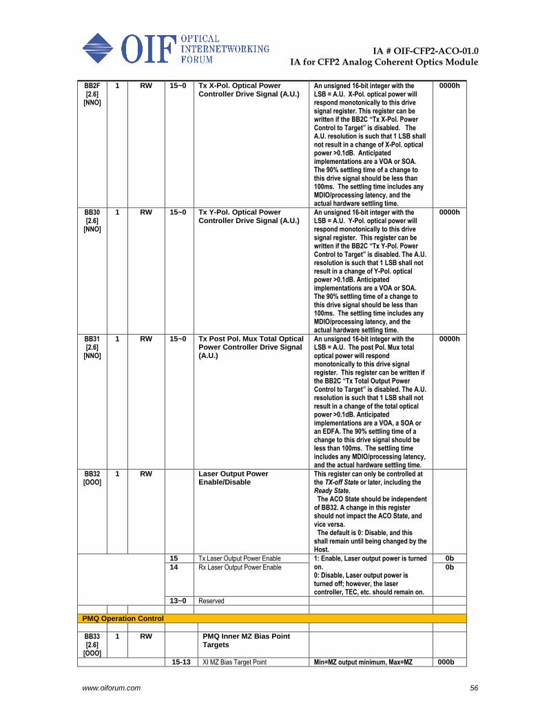
IA # OIF-CFP2-ACO-01.0
IA for CFP2 Analog Coherent Optics Module
www.oiforum.com 56
BB2F [2.6]
[NNO]
1 RW 15~0 Tx X-Pol. Optical Power Controller Drive Signal (A.U.)
An unsigned 16-bit integer with the LSB = A.U. X-Pol. optical power will respond monotonically to this drive signal register. This register can be written if the BB2C “Tx X-Pol. Power Control to Target” is disabled. The A.U. resolution is such that 1 LSB shall not result in a change of X-Pol. optical power >0.1dB. Anticipated implementations are a VOA or SOA. The 90% settling time of a change to this drive signal should be less than 100ms. The settling time includes any MDIO/processing latency, and the actual hardware settling time.
0000h
BB30 [2.6]
[NNO]
1 RW 15~0 Tx Y-Pol. Optical Power Controller Drive Signal (A.U.)
An unsigned 16-bit integer with the LSB = A.U. Y-Pol. optical power will respond monotonically to this drive signal register. This register can be written if the BB2C “Tx Y-Pol. Power Control to Target” is disabled. The A.U. resolution is such that 1 LSB shall not result in a change of Y-Pol. optical power >0.1dB. Anticipated implementations are a VOA or SOA. The 90% settling time of a change to this drive signal should be less than 100ms. The settling time includes any MDIO/processing latency, and the actual hardware settling time.
0000h
BB31 [2.6]
[NNO]
1 RW 15~0 Tx Post Pol. Mux Total Optical Power Controller Drive Signal (A.U.)
An unsigned 16-bit integer with the LSB = A.U. The post Pol. Mux total optical power will respond monotonically to this drive signal register. This register can be written if the BB2C “Tx Total Output Power Control to Target” is disabled. The A.U. resolution is such that 1 LSB shall not result in a change of the total optical power >0.1dB. Anticipated implementations are a VOA, a SOA or an EDFA. The 90% settling time of a change to this drive signal should be less than 100ms. The settling time includes any MDIO/processing latency, and the actual hardware settling time.
0000h
BB32 [OOO]
1 RW Laser Output Power Enable/Disable
This register can only be controlled at the TX-off State or later, including the Ready State. The ACO State should be independent of BB32. A change in this register should not impact the ACO State, and vice versa. The default is 0: Disable, and this shall remain until being changed by the Host.
15 Tx Laser Output Power Enable 1: Enable, Laser output power is turned on. 0: Disable, Laser output power is turned off; however, the laser controller, TEC, etc. should remain on.
0b
14 Rx Laser Output Power Enable 0b
13~0 Reserved
PMQ Operation Control
BB33 [2.6]
[OOO]
1 RW PMQ Inner MZ Bias Point Targets
15-13 XI MZ Bias Target Point Min=MZ output minimum, Max=MZ 000b
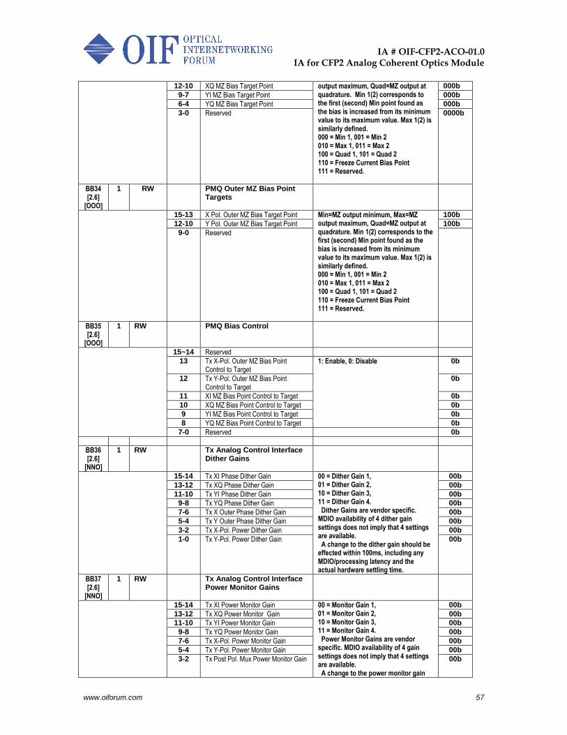
IA # OIF-CFP2-ACO-01.0
IA for CFP2 Analog Coherent Optics Module
www.oiforum.com 57
12-10 XQ MZ Bias Target Point output maximum, Quad=MZ output at quadrature. Min 1(2) corresponds to the first (second) Min point found as the bias is increased from its minimum value to its maximum value. Max 1(2) is similarly defined. 000 = Min 1, 001 = Min 2 010 = Max 1, 011 = Max 2 100 = Quad 1, 101 = Quad 2 110 = Freeze Current Bias Point 111 = Reserved.
000b
9-7 YI MZ Bias Target Point 000b
6-4 YQ MZ Bias Target Point 000b
3-0 Reserved 0000b
BB34 [2.6]
[OOO]
1 RW PMQ Outer MZ Bias Point Targets
15-13 X Pol. Outer MZ Bias Target Point Min=MZ output minimum, Max=MZ output maximum, Quad=MZ output at quadrature. Min 1(2) corresponds to the first (second) Min point found as the bias is increased from its minimum value to its maximum value. Max 1(2) is similarly defined. 000 = Min 1, 001 = Min 2 010 = Max 1, 011 = Max 2 100 = Quad 1, 101 = Quad 2 110 = Freeze Current Bias Point 111 = Reserved.
100b
12-10 Y Pol. Outer MZ Bias Target Point 100b
9-0 Reserved
BB35 [2.6]
[OOO]
1 RW PMQ Bias Control
15~14 Reserved
13 Tx X-Pol. Outer MZ Bias Point Control to Target
1: Enable, 0: Disable 0b
12 Tx Y-Pol. Outer MZ Bias Point Control to Target
0b
11 XI MZ Bias Point Control to Target 0b
10 XQ MZ Bias Point Control to Target 0b
9 YI MZ Bias Point Control to Target 0b
8 YQ MZ Bias Point Control to Target 0b
7-0 Reserved 0b
BB36 [2.6]
[NNO]
1 RW Tx Analog Control Interface Dither Gains
15-14 Tx XI Phase Dither Gain 00 = Dither Gain 1, 01 = Dither Gain 2, 10 = Dither Gain 3, 11 = Dither Gain 4. Dither Gains are vendor specific. MDIO availability of 4 dither gain settings does not imply that 4 settings are available. A change to the dither gain should be effected within 100ms, including any MDIO/processing latency and the actual hardware settling time.
00b
13-12 Tx XQ Phase Dither Gain 00b
11-10 Tx YI Phase Dither Gain 00b
9-8 Tx YQ Phase Dither Gain 00b
7-6 Tx X Outer Phase Dither Gain 00b
5-4 Tx Y Outer Phase Dither Gain 00b
3-2 Tx X-Pol. Power Dither Gain 00b
1-0 Tx Y-Pol. Power Dither Gain 00b
BB37 [2.6]
[NNO]
1 RW Tx Analog Control Interface Power Monitor Gains
15-14 Tx XI Power Monitor Gain 00 = Monitor Gain 1, 01 = Monitor Gain 2, 10 = Monitor Gain 3, 11 = Monitor Gain 4. Power Monitor Gains are vendor specific. MDIO availability of 4 gain settings does not imply that 4 settings are available. A change to the power monitor gain
00b
13-12 Tx XQ Power Monitor Gain 00b
11-10 Tx YI Power Monitor Gain 00b
9-8 Tx YQ Power Monitor Gain 00b
7-6 Tx X-Pol. Power Monitor Gain 00b
5-4 Tx Y-Pol. Power Monitor Gain 00b
3-2 Tx Post Pol. Mux Power Monitor Gain 00b
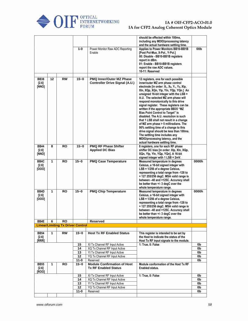
IA # OIF-CFP2-ACO-01.0
IA for CFP2 Analog Coherent Optics Module
www.oiforum.com 58
should be effected within 100ms, including any MDIO/processing latency and the actual hardware settling time.
1-0 Power Monitor Raw ADC Reporting Enable
Applies to Power Monitors BB10-BB1B [Post Pol-Mux, X-Pol., Y-Pol.] 00: Disable - BB10-BB1B registers report in dBm. 01: Enable - BB10-BB1B registers report the raw ADC values. 10-11: Reserved
00b
BB38 [2.6]
[NNO]
12 RW 15~0 PMQ Inner/Outer MZ Phase Controller Drive Signal (A.U.)
12 registers, one for each possible inner/outer MZ arm phase control electrode [in order: XL, XR, YL, YR, XIp, XIn, XQp, XQn, YIp, YIn, YQp, YQn.] An unsigned 16-bit integer with the LSB = A.U. The selected MZ arm phase will respond monotonically to this drive signal register. These registers can be written if the appropriate BB35 “MZ Bias Point Control to Target” is disabled. The A.U. resolution is such that 1 LSB shall not result in a change of MZ arm phase > 5 milliradians. The 90% settling time of a change to this drive signal should be less than 100ms. The settling time includes any MDIO/processing latency, and the actual hardware settling time.
BB44 [2.6]
[NNO]
8 RO 15~0 PMQ RF Phase Shifter Applied DC Bias
8 registers, one for each RF phase shifter DC bias [in order: XIp, XIn, XQp, XQn, YIp, YIn, YQp, YQn]. A 16-bit signed integer with 1 LSB = 2mV.
BB4C [2.6]
[OOO]
1 RO 15~0 PMQ Case Temperature Measured temperature in degrees Celsius, a 16-bit signed integer with LSB = 1/256 of a degree Celsius, representing a total range from -128 to + 127 255/256 degC. MSA valid range is between –40 and +125C. Accuracy shall be better than +/- 3 degC over the whole temperature range.
0000h
BB4D [2.6]
[OOO]
1 RO 15~0 PMQ Chip Temperature Measured temperature in degrees Celsius, a 16-bit signed integer with LSB = 1/256 of a degree Celsius, representing a total range from -128 to + 127 255/256 degC. MSA valid range is between –40 and +125C. Accuracy shall be better than +/- 3 degC over the whole temperature range.
0000h
BB4E 6 RO Reserved
Linear/Limiting Tx Driver Control
BB54 [2.6]
[RRR]
1 RW 15~0 Host Tx RF Enabled Status This register is intended to be set by the Host to indicate the status of the Host Tx RF input signals to the module.
15 XI Tx Channel RF Input Active 1: True, 0: False 0b
14 XQ Tx Channel RF Input Active 0b
13 YI Tx Channel RF Input Active 0b
12 YQ Tx Channel RF Input Active 0b
11-0 Reserved 0b
BB55 [2.6]
[ROO]
1 RO 15~0 Module Confirmation of Host Tx RF Enabled Status
Module conformation of the Host Tx RF Enabled status.
15 XI Tx Channel RF Input Active 1: True, 0: False 0b
14 XQ Tx Channel RF Input Active 0b
13 YI Tx Channel RF Input Active 0b
12 YQ Tx Channel RF Input Active 0b
11-0 Reserved 0b
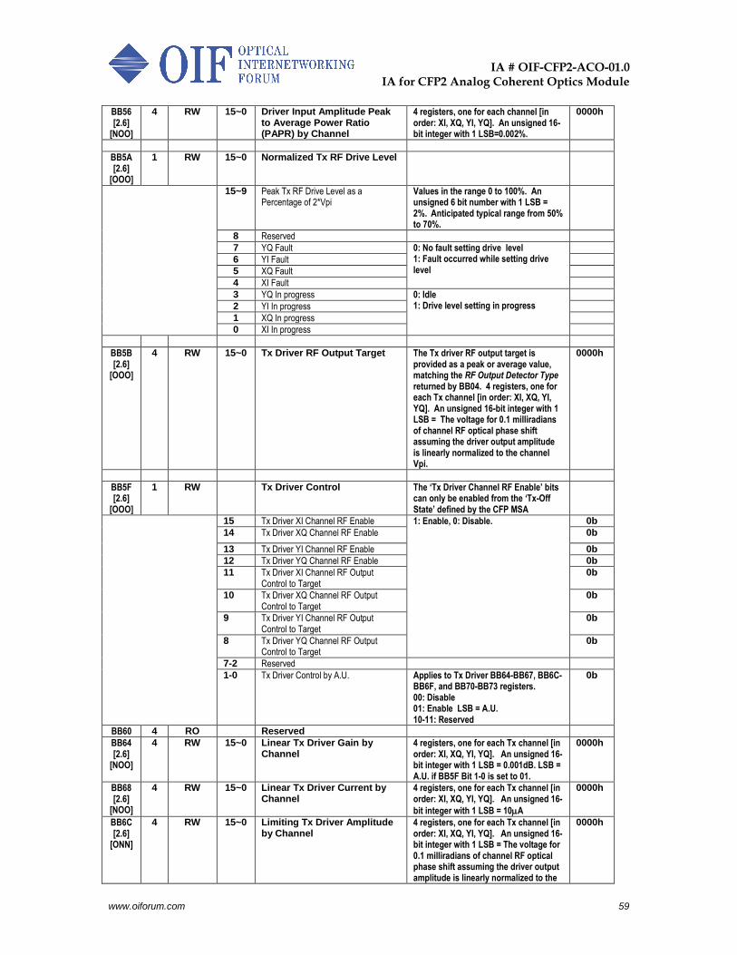
IA # OIF-CFP2-ACO-01.0
IA for CFP2 Analog Coherent Optics Module
www.oiforum.com 59
BB56 [2.6]
[NOO]
4 RW 15~0 Driver Input Amplitude Peak to Average Power Ratio (PAPR) by Channel
4 registers, one for each channel [in order: XI, XQ, YI, YQ]. An unsigned 16-bit integer with 1 LSB=0.002%.
0000h
BB5A [2.6]
[OOO]
1 RW 15~0 Normalized Tx RF Drive Level
15~9 Peak Tx RF Drive Level as a Percentage of 2*Vpi
Values in the range 0 to 100%. An unsigned 6 bit number with 1 LSB = 2%. Anticipated typical range from 50% to 70%.
8 Reserved
7 YQ Fault 0: No fault setting drive level 1: Fault occurred while setting drive level
6 YI Fault
5 XQ Fault
4 XI Fault
3 YQ In progress 0: Idle 1: Drive level setting in progress
2 YI In progress
1 XQ In progress
0 XI In progress
BB5B [2.6]
[OOO]
4 RW 15~0 Tx Driver RF Output Target The Tx driver RF output target is provided as a peak or average value, matching the RF Output Detector Type returned by BB04. 4 registers, one for each Tx channel [in order: XI, XQ, YI, YQ]. An unsigned 16-bit integer with 1 LSB = The voltage for 0.1 milliradians of channel RF optical phase shift assuming the driver output amplitude is linearly normalized to the channel Vpi.
0000h
BB5F [2.6]
[OOO]
1 RW Tx Driver Control The ‘Tx Driver Channel RF Enable’ bits can only be enabled from the ‘Tx-Off State’ defined by the CFP MSA
15 Tx Driver XI Channel RF Enable 1: Enable, 0: Disable.
0b
14 Tx Driver XQ Channel RF Enable 0b
13 Tx Driver YI Channel RF Enable 0b
12 Tx Driver YQ Channel RF Enable 0b
11 Tx Driver XI Channel RF Output Control to Target
0b
10 Tx Driver XQ Channel RF Output Control to Target
0b
9 Tx Driver YI Channel RF Output Control to Target
0b
8 Tx Driver YQ Channel RF Output Control to Target
0b
7-2 Reserved
1-0 Tx Driver Control by A.U. Applies to Tx Driver BB64-BB67, BB6C-BB6F, and BB70-BB73 registers. 00: Disable 01: Enable LSB = A.U. 10-11: Reserved
0b
BB60 4 RO Reserved
BB64 [2.6]
[NOO]
4 RW 15~0 Linear Tx Driver Gain by Channel
4 registers, one for each Tx channel [in order: XI, XQ, YI, YQ]. An unsigned 16-bit integer with 1 LSB = 0.001dB. LSB = A.U. if BB5F Bit 1-0 is set to 01.
0000h
BB68 [2.6]
[NOO]
4 RW 15~0 Linear Tx Driver Current by Channel
4 registers, one for each Tx channel [in order: XI, XQ, YI, YQ]. An unsigned 16-
bit integer with 1 LSB = 10A
0000h
BB6C [2.6]
[ONN]
4 RW 15~0 Limiting Tx Driver Amplitude by Channel
4 registers, one for each Tx channel [in order: XI, XQ, YI, YQ]. An unsigned 16-bit integer with 1 LSB = The voltage for 0.1 milliradians of channel RF optical phase shift assuming the driver output amplitude is linearly normalized to the
0000h
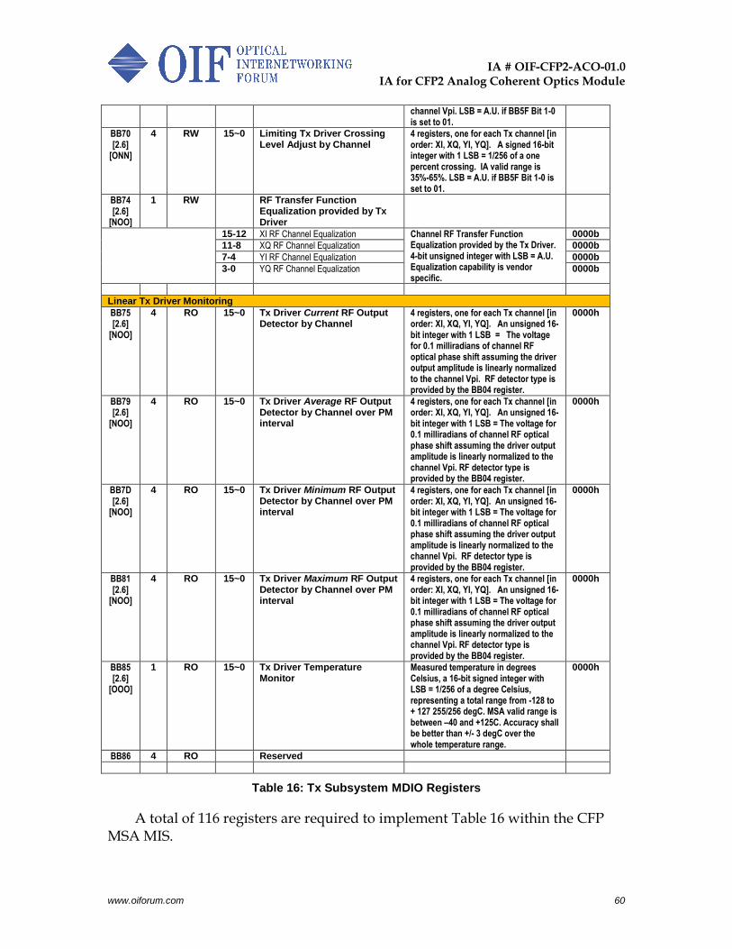
IA # OIF-CFP2-ACO-01.0
IA for CFP2 Analog Coherent Optics Module
www.oiforum.com 60
channel Vpi. LSB = A.U. if BB5F Bit 1-0 is set to 01.
BB70 [2.6]
[ONN]
4 RW 15~0 Limiting Tx Driver Crossing Level Adjust by Channel
4 registers, one for each Tx channel [in order: XI, XQ, YI, YQ]. A signed 16-bit integer with 1 LSB = 1/256 of a one percent crossing. IA valid range is 35%-65%. LSB = A.U. if BB5F Bit 1-0 is set to 01.
BB74 [2.6]
[NOO]
1 RW RF Transfer Function Equalization provided by Tx Driver
15-12 XI RF Channel Equalization Channel RF Transfer Function Equalization provided by the Tx Driver. 4-bit unsigned integer with LSB = A.U. Equalization capability is vendor specific.
0000b
11-8 XQ RF Channel Equalization 0000b
7-4 YI RF Channel Equalization 0000b
3-0 YQ RF Channel Equalization 0000b
Linear Tx Driver Monitoring
BB75 [2.6]
[NOO]
4 RO 15~0 Tx Driver Current RF Output Detector by Channel
4 registers, one for each Tx channel [in order: XI, XQ, YI, YQ]. An unsigned 16-bit integer with 1 LSB = The voltage for 0.1 milliradians of channel RF optical phase shift assuming the driver output amplitude is linearly normalized to the channel Vpi. RF detector type is provided by the BB04 register.
0000h
BB79 [2.6]
[NOO]
4 RO 15~0 Tx Driver Average RF Output Detector by Channel over PM interval
4 registers, one for each Tx channel [in order: XI, XQ, YI, YQ]. An unsigned 16-bit integer with 1 LSB = The voltage for 0.1 milliradians of channel RF optical phase shift assuming the driver output amplitude is linearly normalized to the channel Vpi. RF detector type is provided by the BB04 register.
0000h
BB7D [2.6]
[NOO]
4 RO 15~0 Tx Driver Minimum RF Output Detector by Channel over PM interval
4 registers, one for each Tx channel [in order: XI, XQ, YI, YQ]. An unsigned 16-bit integer with 1 LSB = The voltage for 0.1 milliradians of channel RF optical phase shift assuming the driver output amplitude is linearly normalized to the channel Vpi. RF detector type is provided by the BB04 register.
0000h
BB81 [2.6]
[NOO]
4 RO 15~0 Tx Driver Maximum RF Output Detector by Channel over PM interval
4 registers, one for each Tx channel [in order: XI, XQ, YI, YQ]. An unsigned 16-bit integer with 1 LSB = The voltage for 0.1 milliradians of channel RF optical phase shift assuming the driver output amplitude is linearly normalized to the channel Vpi. RF detector type is provided by the BB04 register.
0000h
BB85 [2.6]
[OOO]
1 RO 15~0 Tx Driver Temperature Monitor
Measured temperature in degrees Celsius, a 16-bit signed integer with LSB = 1/256 of a degree Celsius, representing a total range from -128 to + 127 255/256 degC. MSA valid range is between –40 and +125C. Accuracy shall be better than +/- 3 degC over the whole temperature range.
0000h
BB86 4 RO Reserved
Table 16: Tx Subsystem MDIO Registers
A total of 116 registers are required to implement Table 16 within the CFP MSA MIS.
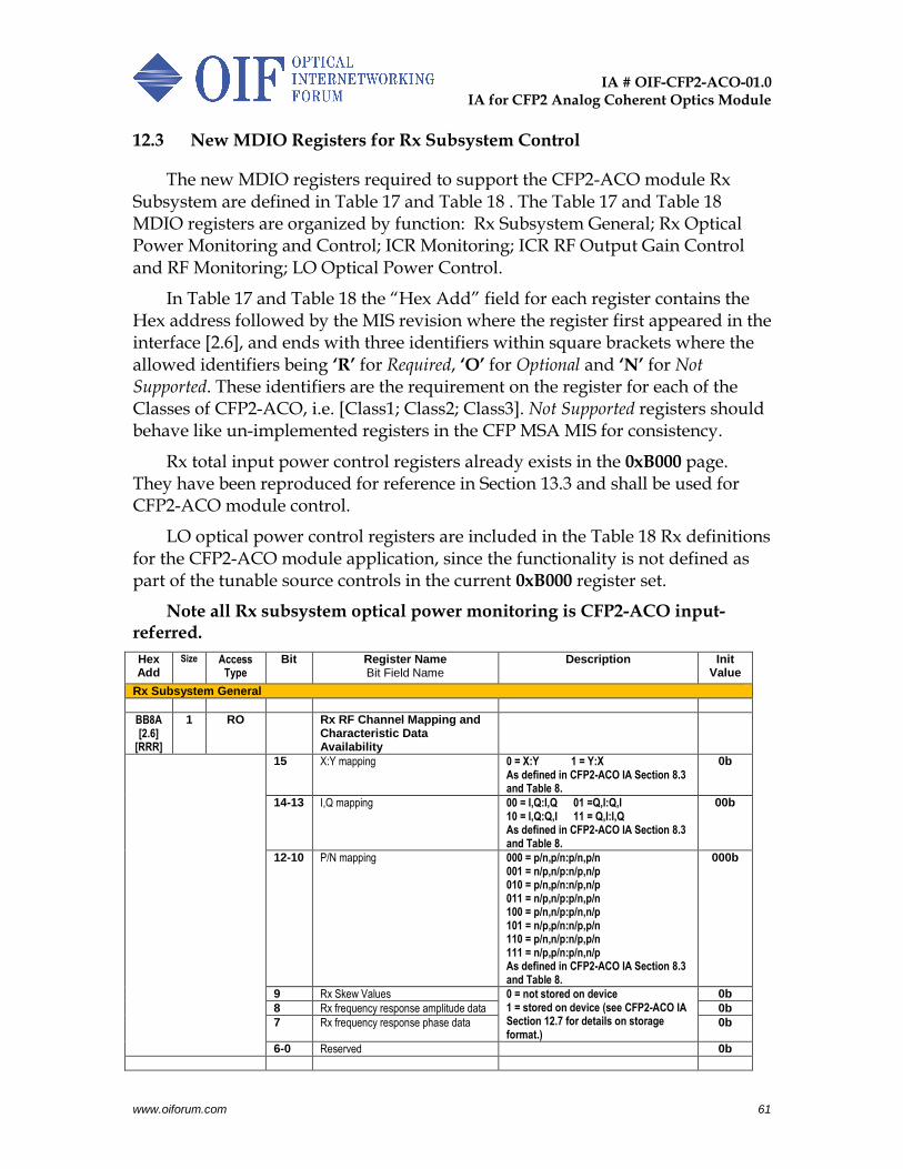
IA # OIF-CFP2-ACO-01.0
IA for CFP2 Analog Coherent Optics Module
www.oiforum.com 61
12.3 New MDIO Registers for Rx Subsystem Control
The new MDIO registers required to support the CFP2-ACO module Rx Subsystem are defined in Table 17 and Table 18 . The Table 17 and Table 18 MDIO registers are organized by function: Rx Subsystem General; Rx Optical Power Monitoring and Control; ICR Monitoring; ICR RF Output Gain Control and RF Monitoring; LO Optical Power Control.
In Table 17 and Table 18 the “Hex Add” field for each register contains the Hex address followed by the MIS revision where the register first appeared in the interface [2.6], and ends with three identifiers within square brackets where the allowed identifiers being ‘R’ for Required, ‘O’ for Optional and ‘N’ for Not Supported. These identifiers are the requirement on the register for each of the Classes of CFP2-ACO, i.e. [Class1; Class2; Class3]. Not Supported registers should behave like un-implemented registers in the CFP MSA MIS for consistency.
Rx total input power control registers already exists in the 0xB000 page. They have been reproduced for reference in Section 13.3 and shall be used for CFP2-ACO module control.
LO optical power control registers are included in the Table 18 Rx definitions for the CFP2-ACO module application, since the functionality is not defined as part of the tunable source controls in the current 0xB000 register set.
Note all Rx subsystem optical power monitoring is CFP2-ACO input-referred.
Hex Add
Size Access Type
Bit Register Name Bit Field Name
Description Init Value
Rx Subsystem General
BB8A [2.6]
[RRR]
1 RO Rx RF Channel Mapping and Characteristic Data Availability
15 X:Y mapping 0 = X:Y 1 = Y:X As defined in CFP2-ACO IA Section 8.3 and Table 8.
0b
14-13 I,Q mapping 00 = I,Q:I,Q 01 =Q,I:Q,I 10 = I,Q:Q,I 11 = Q,I:I,Q As defined in CFP2-ACO IA Section 8.3 and Table 8.
00b
12-10 P/N mapping 000 = p/n,p/n:p/n,p/n 001 = n/p,n/p:n/p,n/p 010 = p/n,p/n:n/p,n/p 011 = n/p,n/p:p/n,p/n 100 = p/n,n/p:p/n,n/p 101 = n/p,p/n:n/p,p/n 110 = p/n,n/p:n/p,p/n 111 = n/p,p/n:p/n,n/p As defined in CFP2-ACO IA Section 8.3 and Table 8.
000b
9 Rx Skew Values 0 = not stored on device 1 = stored on device (see CFP2-ACO IA Section 12.7 for details on storage format.)
0b
8 Rx frequency response amplitude data 0b
7 Rx frequency response phase data 0b
6-0 Reserved 0b
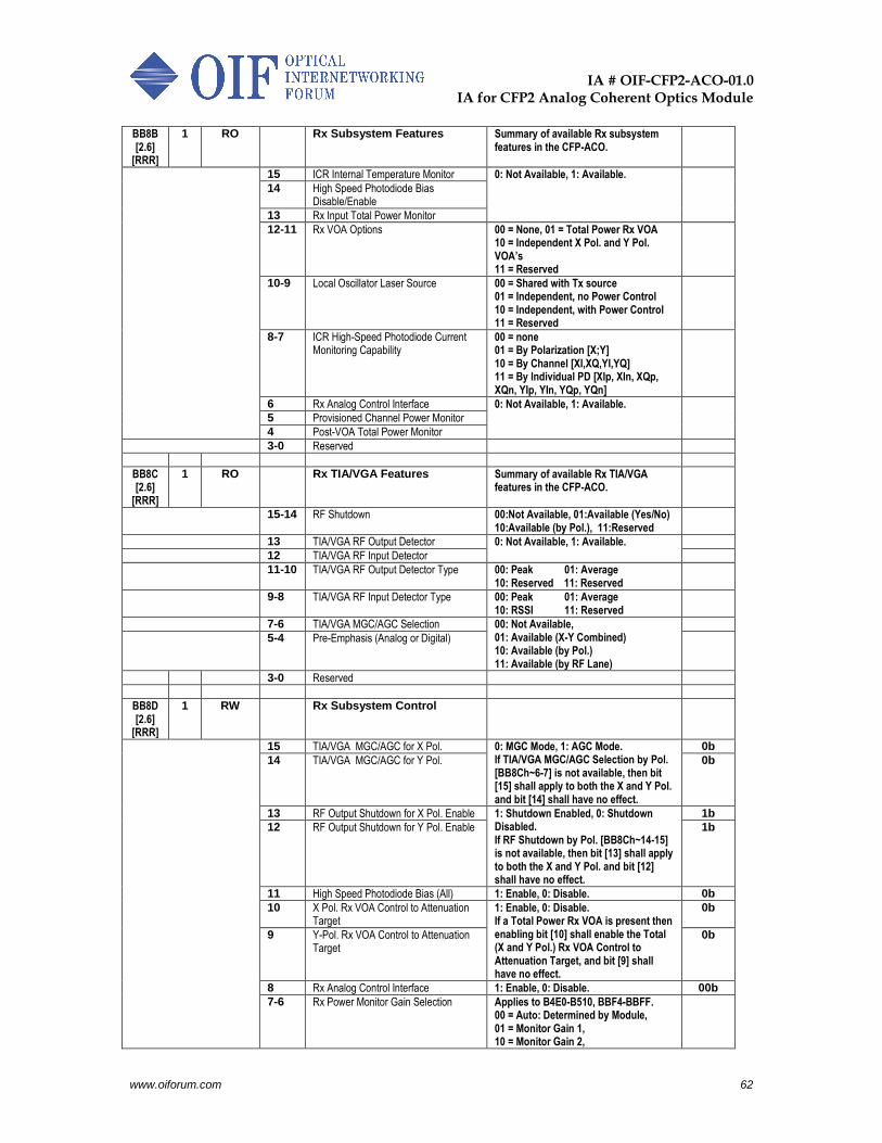
IA # OIF-CFP2-ACO-01.0
IA for CFP2 Analog Coherent Optics Module
www.oiforum.com 62
BB8B [2.6]
[RRR]
1 RO Rx Subsystem Features Summary of available Rx subsystem features in the CFP-ACO.
15 ICR Internal Temperature Monitor 0: Not Available, 1: Available.
14 High Speed Photodiode Bias Disable/Enable
13 Rx Input Total Power Monitor
12-11 Rx VOA Options 00 = None, 01 = Total Power Rx VOA 10 = Independent X Pol. and Y Pol. VOA’s 11 = Reserved
10-9 Local Oscillator Laser Source 00 = Shared with Tx source 01 = Independent, no Power Control 10 = Independent, with Power Control 11 = Reserved
8-7 ICR High-Speed Photodiode Current Monitoring Capability
00 = none 01 = By Polarization [X;Y] 10 = By Channel [XI,XQ,YI,YQ] 11 = By Individual PD [XIp, XIn, XQp, XQn, YIp, YIn, YQp, YQn]
6 Rx Analog Control Interface 0: Not Available, 1: Available.
5 Provisioned Channel Power Monitor
4 Post-VOA Total Power Monitor
3-0 Reserved
BB8C [2.6]
[RRR]
1 RO Rx TIA/VGA Features Summary of available Rx TIA/VGA features in the CFP-ACO.
15-14 RF Shutdown 00:Not Available, 01:Available (Yes/No) 10:Available (by Pol.), 11:Reserved
13 TIA/VGA RF Output Detector 0: Not Available, 1: Available.
12 TIA/VGA RF Input Detector
11-10 TIA/VGA RF Output Detector Type 00: Peak 01: Average 10: Reserved 11: Reserved
9-8 TIA/VGA RF Input Detector Type 00: Peak 01: Average 10: RSSI 11: Reserved
7-6 TIA/VGA MGC/AGC Selection 00: Not Available, 01: Available (X-Y Combined) 10: Available (by Pol.) 11: Available (by RF Lane)
5-4 Pre-Emphasis (Analog or Digital)
3-0 Reserved
BB8D [2.6]
[RRR]
1 RW Rx Subsystem Control
15 TIA/VGA MGC/AGC for X Pol. 0: MGC Mode, 1: AGC Mode. If TIA/VGA MGC/AGC Selection by Pol. [BB8Ch~6-7] is not available, then bit [15] shall apply to both the X and Y Pol. and bit [14] shall have no effect.
0b
14 TIA/VGA MGC/AGC for Y Pol. 0b
13 RF Output Shutdown for X Pol. Enable 1: Shutdown Enabled, 0: Shutdown Disabled. If RF Shutdown by Pol. [BB8Ch~14-15] is not available, then bit [13] shall apply to both the X and Y Pol. and bit [12] shall have no effect.
1b
12 RF Output Shutdown for Y Pol. Enable 1b
11 High Speed Photodiode Bias (All) 1: Enable, 0: Disable. 0b
10 X Pol. Rx VOA Control to Attenuation Target
1: Enable, 0: Disable. If a Total Power Rx VOA is present then enabling bit [10] shall enable the Total (X and Y Pol.) Rx VOA Control to Attenuation Target, and bit [9] shall have no effect.
0b
9 Y-Pol. Rx VOA Control to Attenuation Target
0b
8 Rx Analog Control Interface 1: Enable, 0: Disable. 00b
7-6 Rx Power Monitor Gain Selection Applies to B4E0-B510, BBF4-BBFF. 00 = Auto: Determined by Module, 01 = Monitor Gain 1, 10 = Monitor Gain 2,
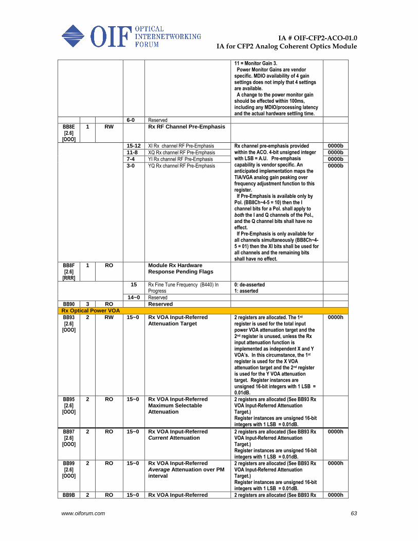
IA # OIF-CFP2-ACO-01.0
IA for CFP2 Analog Coherent Optics Module
www.oiforum.com 63
11 = Monitor Gain 3. Power Monitor Gains are vendor specific. MDIO availability of 4 gain settings does not imply that 4 settings are available. A change to the power monitor gain should be effected within 100ms, including any MDIO/processing latency and the actual hardware settling time.
6-0 Reserved
BB8E [2.6]
[OOO]
1 RW Rx RF Channel Pre-Emphasis
15-12 XI Rx channel RF Pre-Emphasis Rx channel pre-emphasis provided within the ACO. 4-bit unsigned integer with LSB = A.U. Pre-emphasis capability is vendor specific. An anticipated implementation maps the TIA/VGA analog gain peaking over frequency adjustment function to this register. If Pre-Emphasis is available only by Pol. (BB8Ch~4-5 = 10) then the I channel bits for a Pol. shall apply to both the I and Q channels of the Pol., and the Q channel bits shall have no effect. If Pre-Emphasis is only available for all channels simultaneously (BB8Ch~4-5 = 01) then the XI bits shall be used for all channels and the remaining bits shall have no effect.
0000b
11-8 XQ Rx channel RF Pre-Emphasis 0000b
7-4 YI Rx channel RF Pre-Emphasis 0000b
3-0 YQ Rx channel RF Pre-Emphasis 0000b
BB8F [2.6]
[RRR]
1 RO Module Rx Hardware Response Pending Flags
15 Rx Fine Tune Frequency (B440) In Progress
0: de-asserted 1: asserted
14~0 Reserved
BB90 3 RO Reserved
Rx Optical Power VOA
BB93 [2.6]
[OOO]
2 RW 15~0 Rx VOA Input-Referred Attenuation Target
2 registers are allocated. The 1st register is used for the total input power VOA attenuation target and the 2nd register is unused, unless the Rx input attenuation function is implemented as independent X and Y VOA’s. In this circumstance, the 1st register is used for the X VOA attenuation target and the 2nd register is used for the Y VOA attenuation target. Register instances are unsigned 16-bit integers with 1 LSB = 0.01dB.
0000h
BB95 [2.6]
[OOO]
2 RO 15~0 Rx VOA Input-Referred Maximum Selectable Attenuation
2 registers are allocated (See BB93 Rx VOA Input-Referred Attenuation Target.) Register instances are unsigned 16-bit integers with 1 LSB = 0.01dB.
BB97 [2.6]
[OOO]
2 RO 15~0 Rx VOA Input-Referred Current Attenuation
2 registers are allocated (See BB93 Rx VOA Input-Referred Attenuation Target.) Register instances are unsigned 16-bit integers with 1 LSB = 0.01dB.
0000h
BB99 [2.6]
[OOO]
2 RO 15~0 Rx VOA Input-Referred Average Attenuation over PM interval
2 registers are allocated (See BB93 Rx VOA Input-Referred Attenuation Target.) Register instances are unsigned 16-bit integers with 1 LSB = 0.01dB.
0000h
BB9B 2 RO 15~0 Rx VOA Input-Referred 2 registers are allocated (See BB93 Rx 0000h
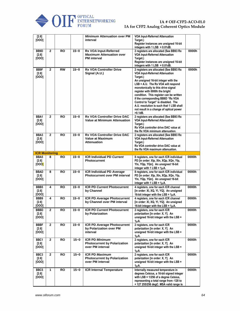
IA # OIF-CFP2-ACO-01.0
IA for CFP2 Analog Coherent Optics Module
www.oiforum.com 64
[2.6] [OOO]
Minimum Attenuation over PM interval
VOA Input-Referred Attenuation Target.) Register instances are unsigned 16-bit integers with 1 LSB = 0.01dB.
BB9D [2.6]
[OOO]
2 RO 15~0 Rx VOA Input-Referred Maximum Attenuation over PM interval
2 registers are allocated (See BB93 Rx VOA Input-Referred Attenuation Target.) Register instances are unsigned 16-bit integers with 1 LSB = 0.01dB.
0000h
BB9F [2.6]
[OOO]
2 RW 15~0 Rx VOA Controller Drive Signal (A.U.)
2 registers are allocated (See BB93 Rx VOA Input-Referred Attenuation Target.) An unsigned 16-bit integer with the LSB = A.U. The Rx VOA will respond monotonically to this drive signal register with 0000h the bright condition. This register can be written if the corresponding BB8D “Rx VOA Control to Target” is disabled. The A.U. resolution is such that 1 LSB shall not result in a change of optical power >0.1dB.
0000h
BBA1 [2.6]
[OOO]
2 RO 15~0 Rx VOA Controller Drive DAC Value at Minimum Attenuation
2 registers are allocated (See BB93 Rx VOA Input-Referred Attenuation Target.) Rx VOA controller drive DAC value at the Rx VOA minimum attenuation.
BBA3 [2.6]
[OOO]
2 RO 15~0 Rx VOA Controller Drive DAC Value at Maximum Attenuation
2 registers are allocated (See BB93 Rx VOA Input-Referred Attenuation Target.) Rx VOA controller drive DAC value at the Rx VOA maximum attenuation.
ICR Monitoring
BBA5 [2.6]
[OOO]
8 RO 15~0 ICR Individual PD Current Photocurrent
8 registers, one for each ICR individual PD [in order: XIp, XIn, XQp, XQn, YIp, YIn, YQp, YQn]. An unsigned 16-bit
integer with 1 LSB = 1A.
0000h
BBAD [2.6]
[OOO]
8 RO 15~0 ICR Individual PD Average Photocurrent over PM interval
8 registers, one for each ICR individual PD [in order: XIp, XIn, XQp, XQn, YIp, YIn, YQp, YQn]. An unsigned 16-bit
integer with 1 LSB = 1A.
0000h
BBB5 [2.6]
[OOO]
4 RO 15~0 ICR PD Current Photocurrent by Channel
4 registers, one for each ICR channel [in order: XI, XQ, YI, YQ]. An unsigned
16-bit integer with the LSB = 1A.
0000h
BBB9 [2.6]
[OOO]
4 RO 15~0 ICR PD Average Photocurrent by Channel over PM interval
4 registers, one for each ICR channel [in order: XI, XQ, YI, YQ]. An unsigned
16-bit integer with the LSB = 1A.
0000h
BBBD [2.6]
[OOO]
2 RO 15~0 ICR PD Current Photocurrent by Polarization
2 registers, one for each ICR polarization [in order: X, Y]. An unsigned 16-bit integer with the LSB =
1A.
0000h
BBBF [2.6]
[OOO]
2 RO 15~0 ICR PD Average Photocurrent by Polarization over PM interval
2 registers, one for each ICR polarization [in order: X, Y]. An unsigned 16-bit integer with the LSB =
1A.
0000h
BBC1 [2.6]
[OOO]
2 RO 15~0 ICR PD Minimum Photocurrent by Polarization over PM interval
2 registers, one for each ICR polarization [in order: X, Y]. An unsigned 16-bit integer with the LSB =
1A.
0000h
BBC3 [2.6]
[OOO]
2 RO 15~0 ICR PD Maximum Photocurrent by Polarization over PM interval
2 registers, one for each ICR polarization [in order: X, Y]. An unsigned 16-bit integer with the LSB =
1A.
0000h
BBC5 [2.6]
[OOO]
1 RO 15~0 ICR Internal Temperature Internally measured temperature in degrees Celsius, a 16-bit signed integer with LSB = 1/256 of a degree Celsius, representing a total range from -128 to + 127 255/256 degC. MSA valid range is
0000h
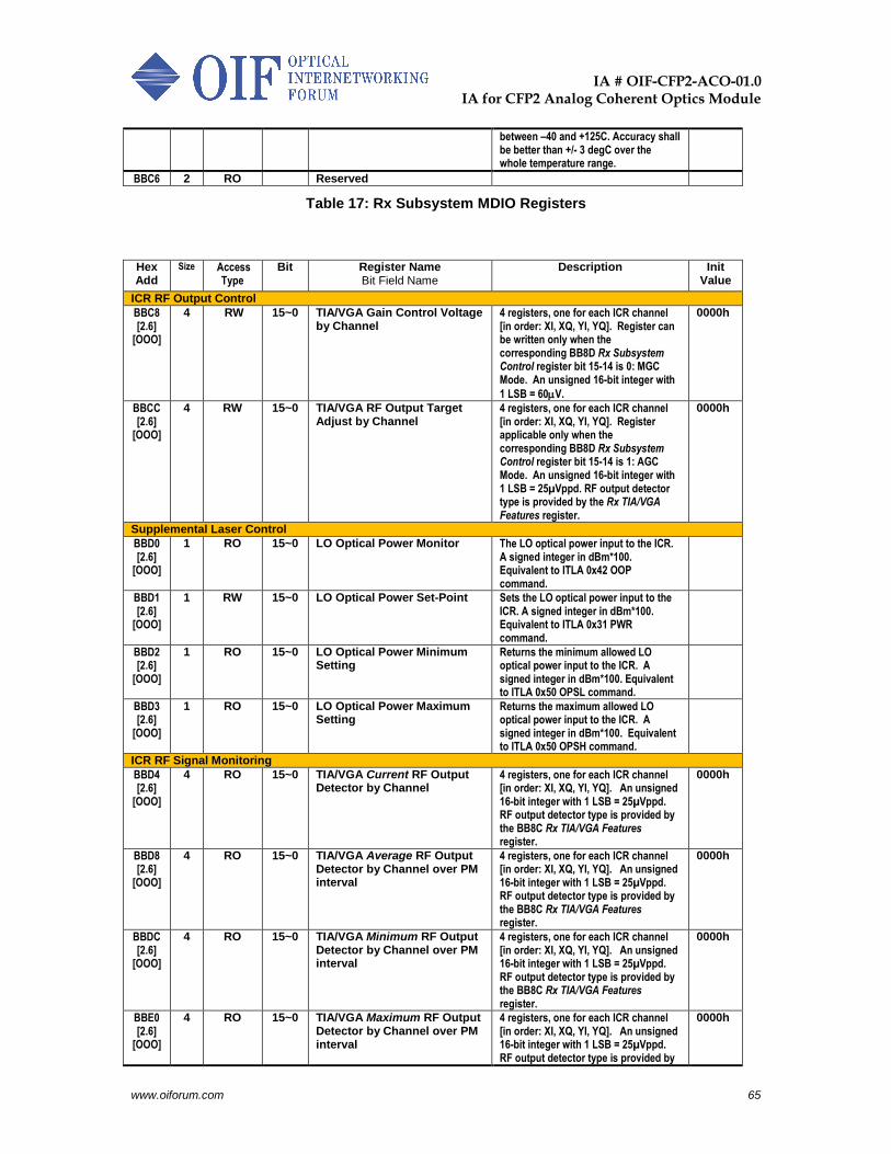
IA # OIF-CFP2-ACO-01.0
IA for CFP2 Analog Coherent Optics Module
www.oiforum.com 65
between –40 and +125C. Accuracy shall be better than +/- 3 degC over the whole temperature range.
BBC6 2 RO Reserved
Table 17: Rx Subsystem MDIO Registers
Hex Add
Size Access Type
Bit Register Name Bit Field Name
Description Init Value
ICR RF Output Control
BBC8 [2.6]
[OOO]
4 RW 15~0 TIA/VGA Gain Control Voltage by Channel
4 registers, one for each ICR channel [in order: XI, XQ, YI, YQ]. Register can be written only when the corresponding BB8D Rx Subsystem Control register bit 15-14 is 0: MGC Mode. An unsigned 16-bit integer with
1 LSB = 60V.
0000h
BBCC [2.6]
[OOO]
4 RW 15~0 TIA/VGA RF Output Target Adjust by Channel
4 registers, one for each ICR channel [in order: XI, XQ, YI, YQ]. Register applicable only when the corresponding BB8D Rx Subsystem Control register bit 15-14 is 1: AGC Mode. An unsigned 16-bit integer with 1 LSB = 25µVppd. RF output detector type is provided by the Rx TIA/VGA Features register.
0000h
Supplemental Laser Control
BBD0 [2.6]
[OOO]
1 RO 15~0 LO Optical Power Monitor The LO optical power input to the ICR. A signed integer in dBm*100. Equivalent to ITLA 0x42 OOP command.
BBD1 [2.6]
[OOO]
1 RW 15~0 LO Optical Power Set-Point Sets the LO optical power input to the ICR. A signed integer in dBm*100. Equivalent to ITLA 0x31 PWR command.
BBD2 [2.6]
[OOO]
1 RO 15~0 LO Optical Power Minimum Setting
Returns the minimum allowed LO optical power input to the ICR. A signed integer in dBm*100. Equivalent to ITLA 0x50 OPSL command.
BBD3 [2.6]
[OOO]
1 RO 15~0 LO Optical Power Maximum Setting
Returns the maximum allowed LO optical power input to the ICR. A signed integer in dBm*100. Equivalent to ITLA 0x50 OPSH command.
ICR RF Signal Monitoring
BBD4 [2.6]
[OOO]
4 RO 15~0 TIA/VGA Current RF Output Detector by Channel
4 registers, one for each ICR channel [in order: XI, XQ, YI, YQ]. An unsigned 16-bit integer with 1 LSB = 25µVppd. RF output detector type is provided by the BB8C Rx TIA/VGA Features register.
0000h
BBD8 [2.6]
[OOO]
4 RO 15~0 TIA/VGA Average RF Output Detector by Channel over PM interval
4 registers, one for each ICR channel [in order: XI, XQ, YI, YQ]. An unsigned 16-bit integer with 1 LSB = 25µVppd. RF output detector type is provided by the BB8C Rx TIA/VGA Features register.
0000h
BBDC [2.6]
[OOO]
4 RO 15~0 TIA/VGA Minimum RF Output Detector by Channel over PM interval
4 registers, one for each ICR channel [in order: XI, XQ, YI, YQ]. An unsigned 16-bit integer with 1 LSB = 25µVppd. RF output detector type is provided by the BB8C Rx TIA/VGA Features register.
0000h
BBE0 [2.6]
[OOO]
4 RO 15~0 TIA/VGA Maximum RF Output Detector by Channel over PM interval
4 registers, one for each ICR channel [in order: XI, XQ, YI, YQ]. An unsigned 16-bit integer with 1 LSB = 25µVppd. RF output detector type is provided by
0000h
IA # OIF-CFP2-ACO-01.0
IA for CFP2 Analog Coherent Optics Module
www.oiforum.com 66
the BB8C Rx TIA/VGA Features register.
BBE4 [2.6]
[OOO]
4 RO 15~0 TIA/VGA Current RF Input Detector by Channel
4 registers, one for each ICR channel [in order: XI, XQ, YI, YQ]. RF input detector type is provided by the BB8C Rx TIA/VGA Features register. For an RSSI type, units are input referred power [dBm], a signed 16-bit integer with 1 LSB=0.01dBm. For Peak and
Mean types, units are Appd, an unsigned 16-bit integer with 1 LSB = 0.1
Appd.
0000h
BBE8 [2.6]
[OOO]
4 RO 15~0 TIA/VGA Average RF Input Detector by Channel over PM interval
4 registers, one for each ICR channel [in order: XI, XQ, YI, YQ]. RF input detector type is provided by the BB8C Rx TIA/VGA Features register. For an RSSI type, units are input referred power [dBm], a signed 16-bit integer with 1 LSB = 0.01dBm. For Peak and
Mean types, units are Appd, an unsigned 16-bit integer with 1 LSB = 0.1
Appd.
0000h
BBEC [2.6]
[OOO]
4 RO 15~0 TIA/VGA Minimum RF Input Detector by Channel over PM interval
4 registers, one for each ICR channel [in order: XI, XQ, YI, YQ]. RF input detector type is provided by the BB8C Rx TIA/VGA Features register. For an RSSI type, units are input referred power [dBm], a signed 16-bit integer with 1 LSB=0.01dBm. For Peak and
Mean types, units are Appd, an unsigned 16-bit integer with 1 LSB = 0.1
Appd.
0000h
BBF0 [2.6]
[OOO]
4 RO 15~0 TIA/VGA Maximum RF Input Detector by Channel over PM interval
4 registers, one for each ICR channel [in order: XI, XQ, YI, YQ]. RF input detector type is provided by the BB8C Rx TIA/VGA Features register. For an RSSI type, units are input referred power [dBm], a signed 16-bit integer with 1 LSB=0.01dBm. For Peak and
Mean types, units are Appd, an unsigned 16-bit integer with 1 LSB = 0.1
Appd.
0000h
Rx Provisioned Channel Power Monitoring [Colorless Line Systems]
BBF4 [2.6]
[OOO]
1 RO 15~0 Current Provisioned Channel Power
The current input power in the provisioned channel. This register will differ from B4E0 in colorless network applications. A signed 16-bit integer with the LSB = 0.01dBm.
BBF5 [2.6]
[OOO]
1 RO 15~0 Average Provisioned Channel Power over PM interval
The average input power in the provisioned channel over the PM interval. This register will differ from B4F0 in colorless network applications. A signed 16-bit integer with the LSB = 0.01dBm.
BBF6 [2.6]
[OOO]
1 RO 15~0 Minimum Provisioned Channel Power over PM interval
The minimum input power in the provisioned channel over the PM interval. This register will differ from B500 in colorless network applications. A signed 16-bit integer with the LSB = 0.01dBm.
BBF7 [2.6]
[OOO]
1 RO 15~0 Maximum Provisioned Channel Power over PM interval
The maximum input power in the provisioned channel over the PM interval. This register will differ from B510 in colorless network applications. A signed 16-bit integer with the LSB = 0.01dBm.
Rx Total Optical Power Monitoring [13.3 Provides Existing MIS Rx Input Power Monitoring Registers]
B4E0 1 RO 15~0 Current Input Power [Total Rx A signed 16-bit integer with the LSB =
IA # OIF-CFP2-ACO-01.0
IA for CFP2 Analog Coherent Optics Module
www.oiforum.com 67
[2.0] [OOO]
Optical] 0.01dBm. [2.6 commentary: Preferred Register for CFP2-ACO Total Current Rx Input Power.]
B4F0 [2.0]
[OOO]
1 RO 15~0 Average Input Power over PM interval [Total Rx Optical]
A signed 16-bit integer with the LSB = 0.01dBm. [2.6 commentary: Preferred Register for CFP2-ACO Average Total Current Rx Input Power.]
B500 [2.0]
[OOO]
1 RO 15~0 Minimum Input Power over PM interval [Total Rx Optical]
A signed 16-bit integer with the LSB = 0.01dBm. [2.6 commentary: Preferred Register for CFP2-ACO Minimum Total Current Rx Input Power.]
B510 [2.0]
[OOO]
1 RO 15~0 Maximum Input Power over PM interval [Total Rx Optical]
A signed 16-bit integer with the LSB = 0.01dBm. [2.6 commentary: Preferred Register for CFP2-ACO Maximum Total Current Rx Input Power.]
BBF8 [2.6]
[OOO]
2 RO 15~0 Current Post-VOA Total Power
2 registers are allocated (See BB93 Rx VOA Input-Referred Attenuation Target.) Register instances are signed 16-bit integers with 1 LSB = 0.01dBm.
BBFA [2.6]
[OOO]
2 RO 15~0 Average Post-VOA Total Power over PM interval
2 registers are allocated (See BB93 Rx VOA Input-Referred Attenuation Target.) Register instances are signed 16-bit integers with 1 LSB = 0.01dBm.
BBFC [2.6]
[OOO]
2 RO 15~0 Minimum Post-VOA Total Power over PM Interval
2 registers are allocated (See BB93 Rx VOA Input-Referred Attenuation Target.) Register instances are signed 16-bit integers with 1 LSB = 0.01dBm.
BBFE [2.6]
[OOO]
2 RO 15~0 Maximum Post-VOA Total Power over PM interval
2 registers are allocated (See BB93 Rx VOA Input-Referred Attenuation Target.) Register instances are signed 16-bit integers with 1 LSB = 0.01dBm.
Table 18: Rx Subsystem MDIO Registers Continued
A total of 112 registers are required to implement Table 17 and Table 18 within the CFP MSA MIS.
12.4 CFP2-ACO Fault, Alarm, Warning and Status (FAWS) Registers
The existing FAWS registers defined for the 0xB000 page in the CFP MSA MIS V2.4 R06b are required for the CFP2-ACO application. In particular for the network lane, B180, B190, B1A0, B1B0, B1C0, B1D0, B1E0, B1F0 and B200 are needed, where n=0.
The Table 16 register BB55 bits 15~12 can be used as error indicators for each of the four GSSG Tx RF channels in the CFP2-ACO application. BB55 is required for CFP2-ACO Class 1, and is optional for Class 2 and Class 3.
Module FAWS register B01D bit 6 for TX_HOST_LOL is the logical OR of all 4 bits in BB55. Register 8074 specifies the usage of B01D bit 6.
The ITLA IA [9] FFreqTh(x024) Fatal Alarm for the loss of frequency control within the required tolerance should be mapped to the ACO MDIO Wavelength Unlock Fault FAWS registers [bit 14 on B1A0, B1D0, B200 with n=0]. When a
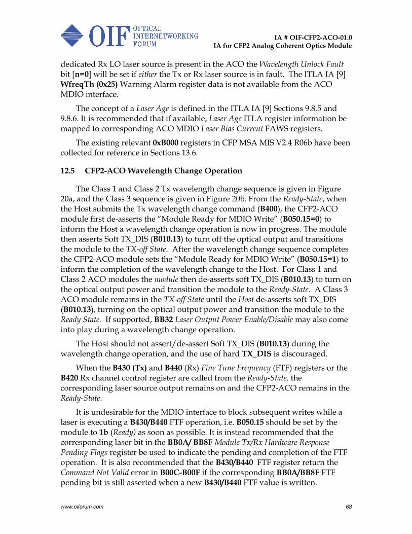
IA # OIF-CFP2-ACO-01.0
IA for CFP2 Analog Coherent Optics Module
www.oiforum.com 68
dedicated Rx LO laser source is present in the ACO the Wavelength Unlock Fault bit [n=0] will be set if either the Tx or Rx laser source is in fault. The ITLA IA [9] WfreqTh (0x25) Warning Alarm register data is not available from the ACO MDIO interface.
The concept of a Laser Age is defined in the ITLA IA [9] Sections 9.8.5 and 9.8.6. It is recommended that if available, Laser Age ITLA register information be mapped to corresponding ACO MDIO Laser Bias Current FAWS registers.
The existing relevant 0xB000 registers in CFP MSA MIS V2.4 R06b have been collected for reference in Sections 13.6.
12.5 CFP2-ACO Wavelength Change Operation
The Class 1 and Class 2 Tx wavelength change sequence is given in Figure 20a, and the Class 3 sequence is given in Figure 20b. From the Ready-State, when the Host submits the Tx wavelength change command (B400), the CFP2-ACO module first de-asserts the “Module Ready for MDIO Write” (B050.15=0) to inform the Host a wavelength change operation is now in progress. The module then asserts Soft TX_DIS (B010.13) to turn off the optical output and transitions the module to the TX-off State. After the wavelength change sequence completes the CFP2-ACO module sets the “Module Ready for MDIO Write” (B050.15=1) to inform the completion of the wavelength change to the Host. For Class 1 and Class 2 ACO modules the module then de-asserts soft TX_DIS (B010.13) to turn on the optical output power and transition the module to the Ready-State. A Class 3 ACO module remains in the TX-off State until the Host de-asserts soft TX_DIS (B010.13), turning on the optical output power and transition the module to the Ready State. If supported, BB32 Laser Output Power Enable/Disable may also come into play during a wavelength change operation.
The Host should not assert/de-assert Soft TX_DIS (B010.13) during the wavelength change operation, and the use of hard TX_DIS is discouraged.
When the B430 (Tx) and B440 (Rx) Fine Tune Frequency (FTF) registers or the B420 Rx channel control register are called from the Ready-State, the corresponding laser source output remains on and the CFP2-ACO remains in the Ready-State.
It is undesirable for the MDIO interface to block subsequent writes while a laser is executing a B430/B440 FTF operation, i.e. B050.15 should be set by the module to 1b (Ready) as soon as possible. It is instead recommended that the corresponding laser bit in the BB0A/ BB8F Module Tx/Rx Hardware Response Pending Flags register be used to indicate the pending and completion of the FTF operation. It is also recommended that the B430/B440 FTF register return the Command Not Valid error in B00C-B00F if the corresponding BB0A/BB8F FTF pending bit is still asserted when a new B430/B440 FTF value is written.
IA # OIF-CFP2-ACO-01.0
IA for CFP2 Analog Coherent Optics Module
www.oiforum.com 69
Figure 20: Wavelength Change Sequence (a) Class 1 and 2, (b) Class 3.
12.6 CFP2-ACO Wavelength Selection Registers
In Ref. [2] the laser source tuning is controlled by a number of registers. The relevant ones are provided in Table 19.
Tx Registers Register Address
Rx Registers Register Address
Tx Channel Control B400 Rx Channel Control B420
Tx Fine Tune Frequency1 B430 Rx Fine Tune Frequency
1 B440
Tx Minimum Laser Frequency 1 818A Rx Minimum Laser Frequency 12 818A
Tx Minimum Laser Frequency 2 818C Rx Minimum Laser Frequency 22 818C
Table 19: CFP MSA MIS V2.4 R06b Laser Control Registers
Notes: 1. Register is optional in Ref. [2]. 2. Minimum frequency for Tx and Rx share the same registers.
The Tx laser frequency as a function of channel number is given by the formula:
Tx Freq(GHz) = (Tx_channel_number-1) * Tx_grid_spacing + Channel_1_frequency +Tx_fine_tune_freq
where: Tx-channel_number is obtained from register B400 bits[9-0]
Tx_grid_spacing is obtained from B400 bits[15-13]
Channel_1_frequency is obtained from register (818A*1000 , 818C/20)
Tx_fine_tune_frequency is register B430/1000
Similarly the Rx laser frequency as a function of channel number is given by the formula:
Rx Freq(GHz) = (Rx_channel_number-1) * Rx_grid_spacing + Channel_1_frequency +Rx_fine_tune_freq
HOST sets Wavelength Change Command (B400h)
CFP asserts soft TX_Disable (B010h.13), clears MOD_READY
Ready State
TX-Turn-off State
HOST de-asserts Soft TX_Disable(B010h.13)
CFP enters TX-Off State
CFP sets Module Ready for MDIO write (B050h.15=1)
CFP clears Module Ready for MDIO write (B050h.15=0)
TX-Off State
TX-Turn-on State
CFP enters Ready State, sets MOD_READY
Ready State
HOST CFP
HOST sets Wavelength Change Command (B400h)
CFP asserts soft TX_Disable(B010h.13), clears MOD_READY
Ready State
TX-Turn-off State
CFP de-asserts Soft TX_Disable (B010h.13)
CFP enters TX-Off State
CFP sets Module Ready for MDIO write (B050h.15=1)
CFP clears Module Ready for MDIO write (B050h.15=0)
TX-Off State
TX-Turn-on State
CFP enters Ready State, sets MOD_READY
Ready State
HOST CFP
a) b)Host should not assert/de-assert Soft
TX_Disable during the wavelength change
operation and the use of hard TX_DIS is
discouraged.
Module changes
wavelengthModule changes
wavelength

IA # OIF-CFP2-ACO-01.0
IA for CFP2 Analog Coherent Optics Module
www.oiforum.com 70
where: Rx-channel_number is obtained from register B420 bits[9-0]
Rx_grid_spacing is obtained from B420 bits[15-13]
Channel_1_frequency is obtained from register (818A*1000 , 818C/20)
Rx_fine_tune_frequency is register B440/1000
The Tx and Rx Fine Tune Frequency registers within the CFP2-ACO are intended to enable fine laser tuning during operation. These registers are expected to be adjusted while the module is carrying traffic and do not require the module to move to a low power or shuttered optical state. The other Tx registers for laser tuning must be used when the laser output is disabled to avoid transmitting signals at frequencies that could affect traffic on other operational channels.
This method of setting the transmit and receive laser frequencies is convenient for the table of gridded frequencies provided in bits[15-13] of registers B400 (for Tx) and B420 (for Rx). If an arbitrary grid or frequency is required, this method has limitations caused particularly by the fact that the two registers controlling the Tx and Rx Minimum Laser Frequency, 818A and 818C are Read-Only registers that are populated at module start up, but are not writable during normal operation.
To facilitate arbitrary frequency tuning with register resolutions down to 1 MHz, a number of additional registers have been requested specifically for the CFP2-ACO module. These registers allow a tuning method similar to Integrable Tunable Laser (ITLA) sources. The requested additional registers are detailed in Section 12.6.1 and in Table 15.
12.6.1 Use of the High Resolution Tuning Registers
The high resolution tuning and arbitrary frequency setting mode is enabled via bit[10] in register B400 (Tx) and B420 (Rx). With bit[10] set to “1” an arbitrary settable Tx or Rx Minimum Laser Frequency is enabled. The two Read-Only registers for the Tx/Rx Minimum Laser Frequency (818A and 818C) are supplemented by 3 Read-Write registers as shown in Table 20. These new registers are Read-Write versions of 818A and 818C and additionally a third register that holds frequency information down to a 1 MHz resolution.
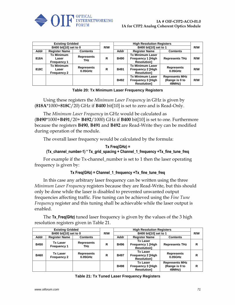
IA # OIF-CFP2-ACO-01.0
IA for CFP2 Analog Coherent Optics Module
www.oiforum.com 71
Existing Gridded
R/W
High Resolution Registers
R/W B400 bit[10] set to 0 B400 bit[10] set to 1
Addr Register Name Contents Addr Register Name Contents
818A Tx Minimum
Laser Frequency 1
Represents THz
R B490 Tx Minimum Laser Frequency 1 [High
Resolution] Represents THz R/W
818C Tx Minimum
Laser Frequency 2
Represents 0.05GHz
R B491 Tx Minimum Laser Frequency 2 [High
Resolution]
Represents 0.05GHz
R/W
B492
Tx Minimum Laser Frequency 3 [High
Resolution]
Represents MHz (Range is 0 to
49MHz) R/W
Table 20: Tx Minimum Laser Frequency Registers
Using these registers the Minimum Laser Frequency in GHz is given by (818A*1000+818C/20) GHz if B400 bit[10] is set to zero and is Read-Only.
The Minimum Laser Frequency in GHz would be calculated as (B490*1000+B491/20+ B492/1000) GHz if B400 bit[10] is set to one. Furthermore because the registers B490, B491 and B492 are Read-Write they can be modified during operation of the module.
The overall laser frequency would be calculated by the formula:
Tx Freq(GHz) = (Tx_channel_number-1) * Tx_grid_spacing + Channel_1_frequency +Tx_fine_tune_freq
For example if the Tx-channel_number is set to 1 then the laser operating frequency is given by:
Tx Freq(GHz) = Channel_1_frequency +Tx_fine_tune_freq
In this case any arbitrary laser frequency can be written using the three Minimum Laser Frequency registers because they are Read-Write, but this should only be done while the laser is disabled to prevented unwanted output frequencies affecting traffic. Fine tuning can be achieved using the Fine Tune Frequency register and this tuning shall be achievable while the laser output is enabled.
The Tx_Freq(GHz) tuned laser frequency is given by the values of the 3 high resolution registers given in Table 21.
Existing Gridded
R/W
High Resolution Registers
R/W B400 bit[10] set to 0 B400 bit[10] set to 1
Addr Register Name Contents Addr Register Name Contents
B450 Tx Laser
Frequency 1 Represents
THz R B496
Tx Laser Frequency 1 [High
Resolution] Represents THz R
B460 Tx Laser
Frequency 2 Represents
0.05GHz R B497
Tx Laser Frequency 2 [High
Resolution]
Represents 0.05GHz
R
B498
Tx Laser Frequency 3 [High
Resolution]
Represents MHz (Range is 0 to
49MHz) R
Table 21: Tx Tuned Laser Frequency Registers
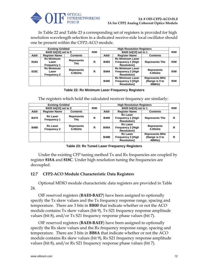
IA # OIF-CFP2-ACO-01.0
IA for CFP2 Analog Coherent Optics Module
www.oiforum.com 72
In Table 22 and Table 23 a corresponding set of registers is provided for high resolution wavelength selection in a dedicated receive-side local oscillator should one be present within the CFP2-ACO module.
Existing Gridded
R/W
High Resolution Registers
R/W B420 bit[10] set to 0 B420 bit[10] set to 1
Addr Register Name Contents Addr Register Name Contents
818A Rx Minimum
Laser Frequency 1
Represents THz
R B493 Rx Minimum Laser Frequency 1 [High
Resolution] Represents THz R/W
818C Rx Minimum
Laser Frequency 2
Represents 0.05GHz
R B494 Rx Minimum Laser Frequency 2 [High
Resolution]
Represents 0.05GHz
R/W
B495
Rx Minimum Laser Frequency 3 [High
Resolution]
Represents MHz (Range is 0 to
49MHz) R/W
Table 22: Rx Minimum Laser Frequency Registers
The registers which hold the calculated receiver frequency are similarly:
Existing Gridded
R/W
High Resolution Registers
R/W B420 bit[10] set to 0 B420 bit[10] set to 1
Addr Register Name Contents Addr Register Name Contents
B470 Rx Laser
Frequency 1 Represents
THz R B499
Rx Laser Frequency 1 [High
Resolution] Represents THz R
B480 Rx Laser
Frequency 2 Represents
0.05GHz R B49A
Rx Laser Frequency 2 [High
Resolution]
Represents 0.05GHz
R
B49B
Rx Laser Frequency 3 [High
Resolution]
Represents MHz (Range is 0 to
49MHz) R
Table 23: Rx Tuned Laser Frequency Registers
Under the existing CFP tuning method Tx and Rx frequencies are coupled by register 818A and 818C. Under high resolution tuning the frequencies are decoupled.
12.7 CFP2-ACO Module Characteristic Data Registers
Optional MDIO module characteristic data registers are provided in Table 24.
OIF reserved registers (BAE0-BAE7) have been assigned to optionally specify the Tx skew values and the Tx frequency response range, spacing and temperature. There are 3 bits in BB00 that indicate whether or not the ACO module contains Tx skew values (bit 9), Tx S21 frequency response amplitude values (bit 8), and/or Tx S21 frequency response phase values (bit 7).
OIF reserved registers (BAE8-BAEF) have been assigned to optionally specify the Rx skew values and the Rx frequency response range, spacing and temperature. There are 3 bits in BB8A that indicate whether or not the ACO module contains Rx skew values (bit 9), Rx S21 frequency response amplitude values (bit 8), and/or Rx S21 frequency response phase values (bit 7).
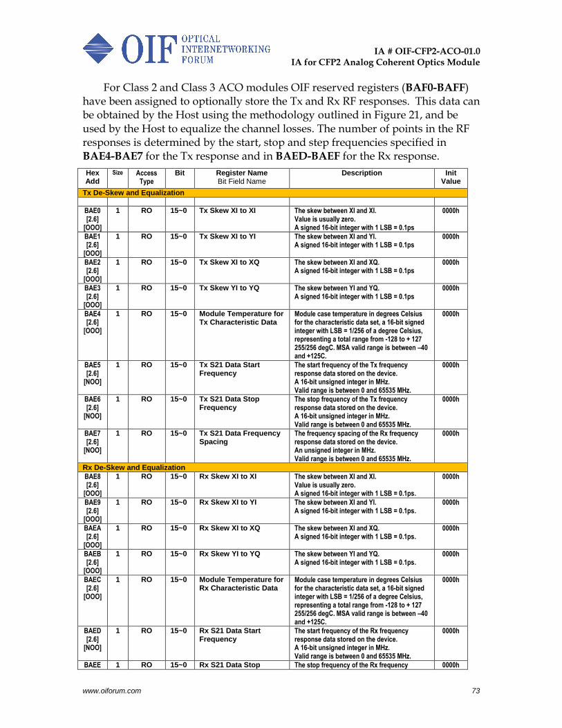
IA # OIF-CFP2-ACO-01.0
IA for CFP2 Analog Coherent Optics Module
www.oiforum.com 73
For Class 2 and Class 3 ACO modules OIF reserved registers (BAF0-BAFF) have been assigned to optionally store the Tx and Rx RF responses. This data can be obtained by the Host using the methodology outlined in Figure 21, and be used by the Host to equalize the channel losses. The number of points in the RF responses is determined by the start, stop and step frequencies specified in BAE4-BAE7 for the Tx response and in BAED-BAEF for the Rx response.
Hex Add
Size Access Type
Bit Register Name Bit Field Name
Description Init Value
Tx De-Skew and Equalization
BAE0 [2.6]
[OOO]
1 RO 15~0 Tx Skew XI to XI The skew between XI and XI. Value is usually zero. A signed 16-bit integer with 1 LSB = 0.1ps
0000h
BAE1 [2.6]
[OOO]
1 RO 15~0 Tx Skew XI to YI The skew between XI and YI. A signed 16-bit integer with 1 LSB = 0.1ps
0000h
BAE2 [2.6]
[OOO]
1 RO 15~0 Tx Skew XI to XQ The skew between XI and XQ. A signed 16-bit integer with 1 LSB = 0.1ps
0000h
BAE3 [2.6]
[OOO]
1 RO 15~0 Tx Skew YI to YQ The skew between YI and YQ. A signed 16-bit integer with 1 LSB = 0.1ps
0000h
BAE4 [2.6]
[OOO]
1 RO 15~0 Module Temperature for Tx Characteristic Data
Module case temperature in degrees Celsius for the characteristic data set, a 16-bit signed integer with LSB = 1/256 of a degree Celsius, representing a total range from -128 to + 127 255/256 degC. MSA valid range is between –40 and +125C.
0000h
BAE5 [2.6]
[NOO]
1 RO 15~0 Tx S21 Data Start Frequency
The start frequency of the Tx frequency response data stored on the device. A 16-bit unsigned integer in MHz. Valid range is between 0 and 65535 MHz.
0000h
BAE6 [2.6]
[NOO]
1 RO 15~0 Tx S21 Data Stop Frequency
The stop frequency of the Tx frequency response data stored on the device. A 16-bit unsigned integer in MHz. Valid range is between 0 and 65535 MHz.
0000h
BAE7 [2.6]
[NOO]
1 RO 15~0 Tx S21 Data Frequency Spacing
The frequency spacing of the Rx frequency response data stored on the device. An unsigned integer in MHz. Valid range is between 0 and 65535 MHz.
0000h
Rx De-Skew and Equalization
BAE8 [2.6]
[OOO]
1 RO 15~0 Rx Skew XI to XI The skew between XI and XI. Value is usually zero. A signed 16-bit integer with 1 LSB = 0.1ps.
0000h
BAE9 [2.6]
[OOO]
1 RO 15~0 Rx Skew XI to YI The skew between XI and YI. A signed 16-bit integer with 1 LSB = 0.1ps.
0000h
BAEA [2.6]
[OOO]
1 RO 15~0 Rx Skew XI to XQ The skew between XI and XQ. A signed 16-bit integer with 1 LSB = 0.1ps.
0000h
BAEB [2.6]
[OOO]
1 RO 15~0 Rx Skew YI to YQ The skew between YI and YQ. A signed 16-bit integer with 1 LSB = 0.1ps.
0000h
BAEC [2.6]
[OOO]
1 RO 15~0 Module Temperature for Rx Characteristic Data
Module case temperature in degrees Celsius for the characteristic data set, a 16-bit signed integer with LSB = 1/256 of a degree Celsius, representing a total range from -128 to + 127 255/256 degC. MSA valid range is between –40 and +125C.
0000h
BAED [2.6]
[NOO]
1 RO 15~0 Rx S21 Data Start Frequency
The start frequency of the Rx frequency response data stored on the device. A 16-bit unsigned integer in MHz. Valid range is between 0 and 65535 MHz.
0000h
BAEE 1 RO 15~0 Rx S21 Data Stop The stop frequency of the Rx frequency 0000h
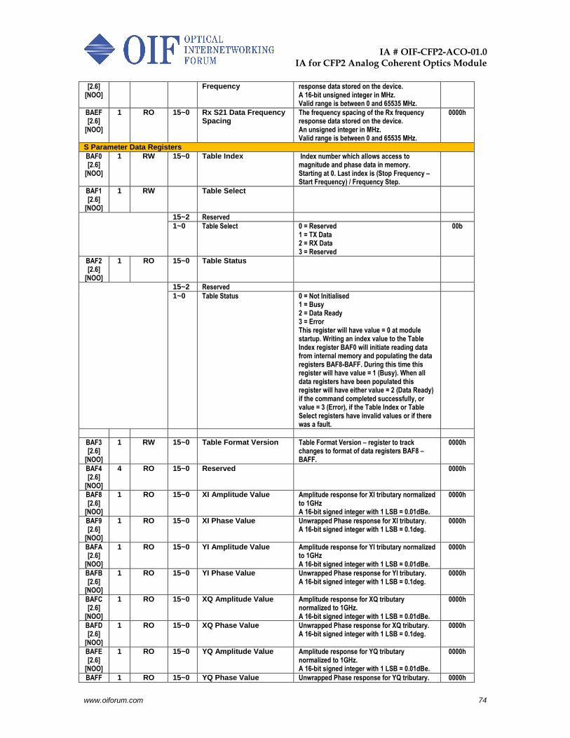
IA # OIF-CFP2-ACO-01.0
IA for CFP2 Analog Coherent Optics Module
www.oiforum.com 74
[2.6] [NOO]
Frequency response data stored on the device. A 16-bit unsigned integer in MHz. Valid range is between 0 and 65535 MHz.
BAEF [2.6]
[NOO]
1 RO 15~0 Rx S21 Data Frequency Spacing
The frequency spacing of the Rx frequency response data stored on the device. An unsigned integer in MHz. Valid range is between 0 and 65535 MHz.
0000h
S Parameter Data Registers
BAF0 [2.6]
[NOO]
1 RW 15~0 Table Index Index number which allows access to magnitude and phase data in memory. Starting at 0. Last index is (Stop Frequency – Start Frequency) / Frequency Step.
BAF1 [2.6]
[NOO]
1 RW Table Select
15~2 Reserved
1~0 Table Select 0 = Reserved 1 = TX Data 2 = RX Data 3 = Reserved
00b
BAF2 [2.6]
[NOO]
1 RO 15~0 Table Status
15~2 Reserved
1~0 Table Status 0 = Not Initialised 1 = Busy 2 = Data Ready 3 = Error This register will have value = 0 at module startup. Writing an index value to the Table Index register BAF0 will initiate reading data from internal memory and populating the data registers BAF8-BAFF. During this time this register will have value = 1 (Busy). When all data registers have been populated this register will have either value = 2 (Data Ready) if the command completed successfully, or value = 3 (Error), if the Table Index or Table Select registers have invalid values or if there was a fault.
BAF3 [2.6]
[NOO]
1 RW 15~0 Table Format Version Table Format Version – register to track changes to format of data registers BAF8 – BAFF.
0000h
BAF4 [2.6]
[NOO]
4 RO 15~0 Reserved 0000h
BAF8 [2.6]
[NOO]
1 RO 15~0 XI Amplitude Value Amplitude response for XI tributary normalized to 1GHz A 16-bit signed integer with 1 LSB = 0.01dBe.
0000h
BAF9 [2.6]
[NOO]
1 RO 15~0 XI Phase Value Unwrapped Phase response for XI tributary. A 16-bit signed integer with 1 LSB = 0.1deg.
0000h
BAFA [2.6]
[NOO]
1 RO 15~0 YI Amplitude Value Amplitude response for YI tributary normalized to 1GHz A 16-bit signed integer with 1 LSB = 0.01dBe.
0000h
BAFB [2.6]
[NOO]
1 RO 15~0 YI Phase Value Unwrapped Phase response for YI tributary. A 16-bit signed integer with 1 LSB = 0.1deg.
0000h
BAFC [2.6]
[NOO]
1 RO 15~0 XQ Amplitude Value Amplitude response for XQ tributary normalized to 1GHz. A 16-bit signed integer with 1 LSB = 0.01dBe.
0000h
BAFD [2.6]
[NOO]
1 RO 15~0 XQ Phase Value Unwrapped Phase response for XQ tributary. A 16-bit signed integer with 1 LSB = 0.1deg.
0000h
BAFE [2.6]
[NOO]
1 RO 15~0 YQ Amplitude Value Amplitude response for YQ tributary normalized to 1GHz. A 16-bit signed integer with 1 LSB = 0.01dBe.
0000h
BAFF 1 RO 15~0 YQ Phase Value Unwrapped Phase response for YQ tributary. 0000h
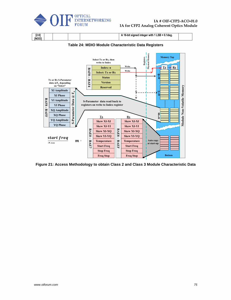
IA # OIF-CFP2-ACO-01.0
IA for CFP2 Analog Coherent Optics Module
www.oiforum.com 75
[2.6] [NOO]
A 16-bit signed integer with 1 LSB = 0.1deg.
Table 24: MDIO Module Characteristic Data Registers
Figure 21: Access Methodology to obtain Class 2 and Class 3 Module Characteristic Data
Memory Top
Bottom
Mo
du
le N
on
-Vo
lati
le M
emo
ry
XI Amplitude
XI Phase
YI Amplitude
YI Phase
XQ Amplitude
XQ Phase
YQ Amplitude
YQ Phase
S-P
ara
met
er D
ata
@ F
n
Tx Rx
n=
0n
=1
……
.
……
.
Tx or Rx S-Parameter
data @Fn depending
on “Select”
BA
F8
-B
AF
F
Index: n
Select: Tx or Rx
Status
Version
Reserved
BA
F0
–B
AF
4
Bottom
Skew XI-XI
Skew XI-YI
Skew XI-XQ
Skew YI-YQ
Temperature
Start Freq
Freq Step
Stop Freq
Rx
BA
E8
–B
AE
F
Skew XI-XI
Skew XI-YI
Skew XI-XQ
Skew YI-YQ
Temperature
Start Freq
Freq Step
Stop Freq
Tx
BA
E0
–B
AE
7
Ph
ysi
cal M
emo
ry
Reg
iste
rs
Auto copy
at start-up
Select Tx or Rx, then
write to Index
n=
m
Write
Write
S-Parameter data read back to
registers on write to Index register
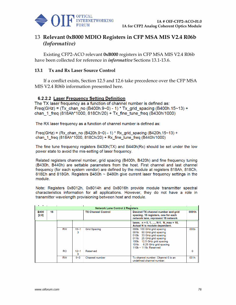
IA # OIF-CFP2-ACO-01.0
IA for CFP2 Analog Coherent Optics Module
www.oiforum.com 76
Relevant 0xB000 MDIO Registers in CFP MSA MIS V2.4 R06b 13(Informative)
Existing CFP2-ACO relevant 0xB000 registers in CFP MSA MIS V2.4 R06b have been collected for reference in informative Sections 13.1-13.6.
13.1 Tx and Rx Laser Source Control
If a conflict exists, Section 12.5 and 12.6 take precedence over the CFP MSA MIS V2.4 R06b information presented here.
IA # OIF-CFP2-ACO-01.0
IA for CFP2 Analog Coherent Optics Module
www.oiforum.com 77
IA # OIF-CFP2-ACO-01.0
IA for CFP2 Analog Coherent Optics Module
www.oiforum.com 78
13.2 Tx and Rx Laser Source Performance Monitoring
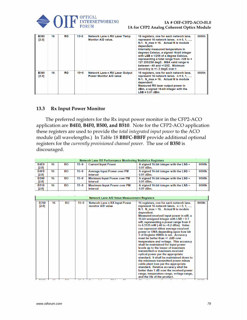
IA # OIF-CFP2-ACO-01.0
IA for CFP2 Analog Coherent Optics Module
www.oiforum.com 79
13.3 Rx Input Power Monitor
The preferred registers for the Rx input power monitor in the CFP2-ACO application are B4E0, B4F0, B500, and B510. Note for the CFP2-ACO application these registers are used to provide the total integrated input power to the ACO module (all wavelengths.) In Table 18 BBFC-BBFF provide additional optional registers for the currently provisioned channel power. The use of B350 is discouraged.
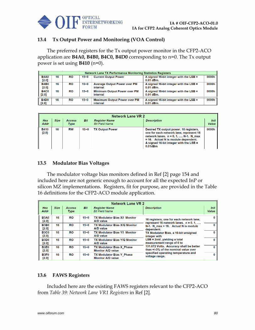
IA # OIF-CFP2-ACO-01.0
IA for CFP2 Analog Coherent Optics Module
www.oiforum.com 80
13.4 Tx Output Power and Monitoring (VOA Control)
The preferred registers for the Tx output power monitor in the CFP2-ACO application are B4A0, B4B0, B4C0, B4D0 corresponding to n=0. The Tx output power is set using B410 (n=0).
13.5 Modulator Bias Voltages
The modulator voltage bias monitors defined in Ref [2] page 154 and included here are not generic enough to account for all the expected InP or silicon MZ implementations. Registers, fit for purpose, are provided in the Table 16 definitions for the CFP2-ACO module application.
13.6 FAWS Registers
Included here are the existing FAWS registers relevant to the CFP2-ACO from Table 39: Network Lane VR1 Registers in Ref [2].
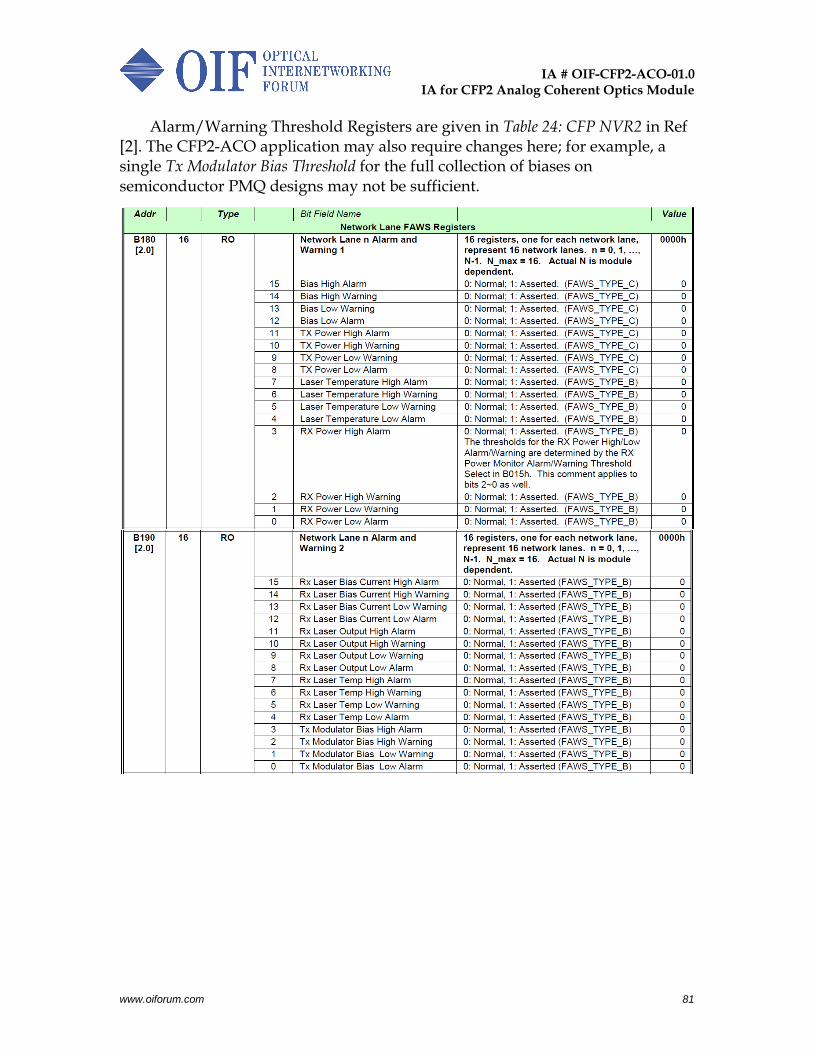
IA # OIF-CFP2-ACO-01.0
IA for CFP2 Analog Coherent Optics Module
www.oiforum.com 81
Alarm/Warning Threshold Registers are given in Table 24: CFP NVR2 in Ref [2]. The CFP2-ACO application may also require changes here; for example, a single Tx Modulator Bias Threshold for the full collection of biases on semiconductor PMQ designs may not be sufficient.
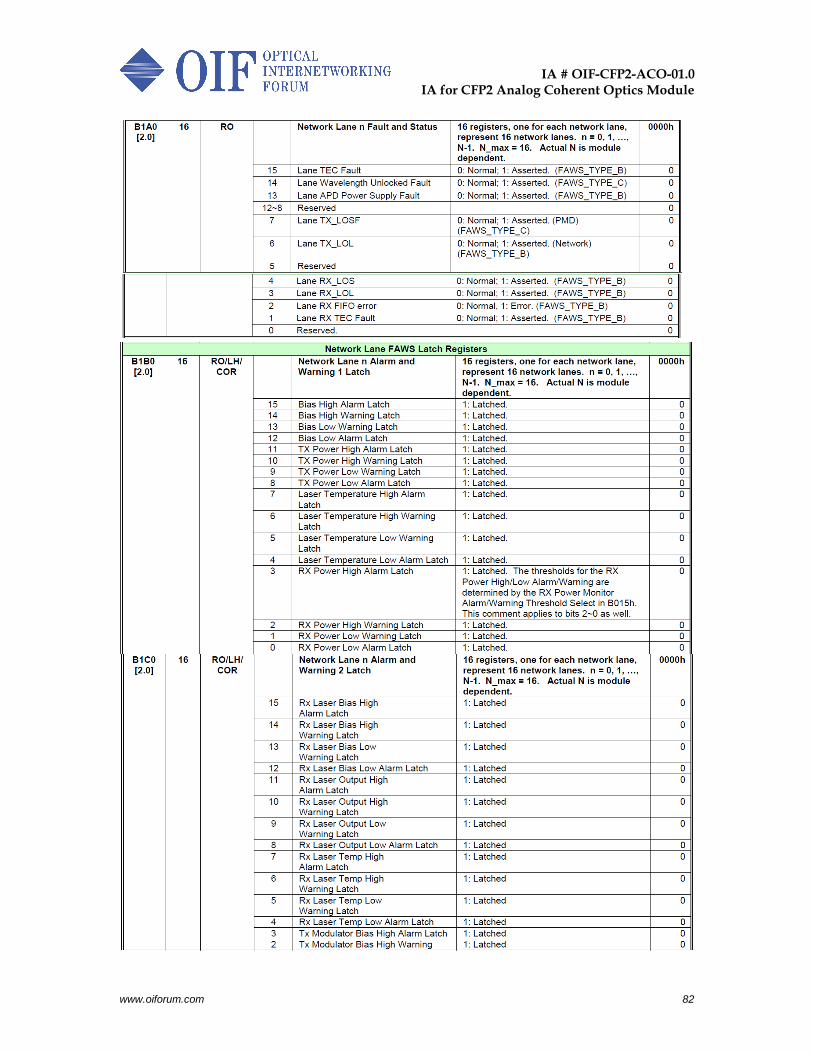
IA # OIF-CFP2-ACO-01.0
IA for CFP2 Analog Coherent Optics Module
www.oiforum.com 82
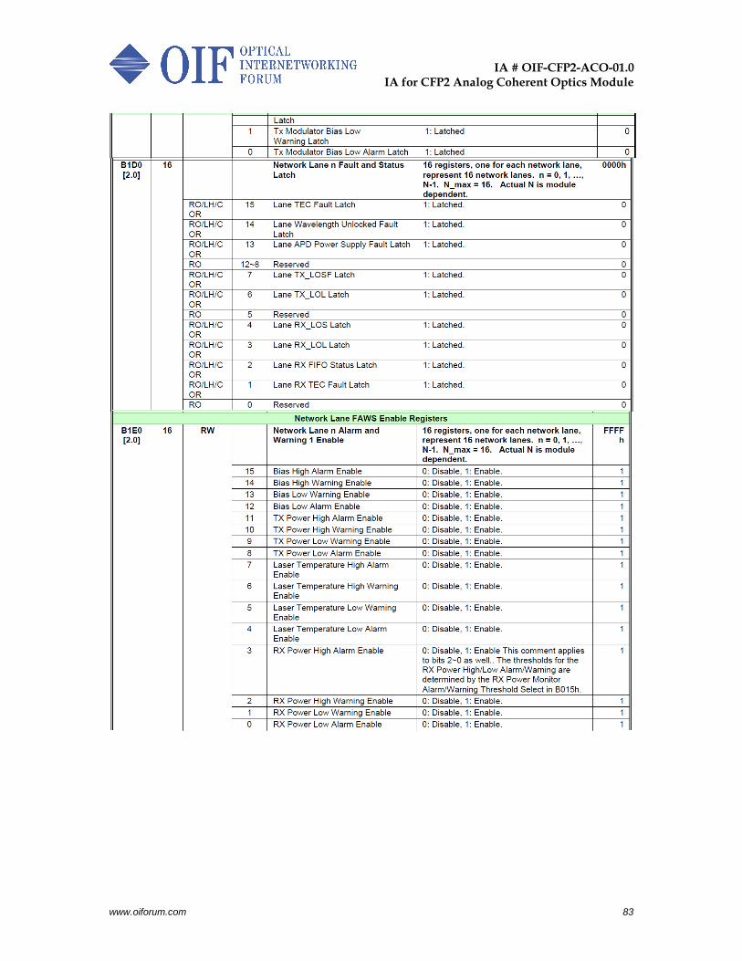
IA # OIF-CFP2-ACO-01.0
IA for CFP2 Analog Coherent Optics Module
www.oiforum.com 83
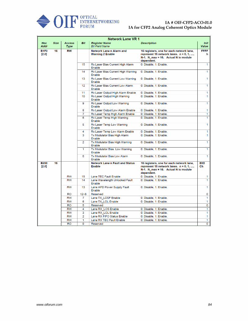
IA # OIF-CFP2-ACO-01.0
IA for CFP2 Analog Coherent Optics Module
www.oiforum.com 84
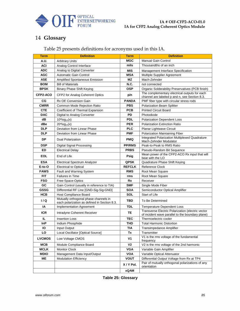
IA # OIF-CFP2-ACO-01.0
IA for CFP2 Analog Coherent Optics Module
www.oiforum.com 85
Glossary 14
Table 25 presents definitions for acronyms used in this IA.
Term Definition Term Definition
A.U. Arbitrary Units MGC Manual Gain Control
ACI Analog Control Interface mils Thousandths of an inch
ADC Analog to Digital Converter MIS Management Interface Specification
AGC Automatic Gain Control MSA Multiple Supplier Agreement
ASE Amplified Spontaneous Emission MZ Mach-Zehnder
BOM Bill of Materials N.C. not connected
BPSK Binary Phase Shift Keying OSP Organic Solderability Preservatives (PCB finish)
CFP2-ACO CFP2 for Analog Coherent Optics p/n The complementary electrical outputs for each channel are labeled p and n, see Section 8.3.
CG Rx OE Conversion Gain PANDA PMF fiber type with circular stress rods
CMRR Common Mode Rejection Ratio PBS Polarization Beam Splitter
CTE Coefficient of Thermal Expansion PCB Printed Circuit Board
DAC Digital to Analog Converter PD Photodiode
dB 10*log10(x) PDL Polarization Dependent Loss
dBe 20*log10(x) PER Polarization Extinction Ratio
DLP Deviation from Linear Phase PLC Planar Lightwave Circuit
DLP Deviation from Linear Phase PMF Polarization Maintaining Fiber
DP Dual Polarization PMQ Integrated Polarization Multiplexed Quadrature Mach-Zehnder Modulator
DSP Digital Signal Processing PP/RMS Peak-to-Peak to RMS Ratio
ED Electrical Delay PRBS Pseudo-Random Bit Sequence
EOL End of Life Psig Mean power of the CFP2-ACO Rx input that will beat with the LO
ESA Electrical Spectrum Analyzer QPSK Quadrature Phase Shift Keying
E-to-O Electrical to Optical REFCLK Reference Clock
FAWS Fault and Warning System RMS Root Mean Square
FIT Failures in Time rms Root Mean Square
FSO Free-Space-Optics Rx Receiver
GC Gain Control (usually in reference to TIA) SMF Single Mode Fiber
GSSG Differential RF Line [GND-Sig-Sig-GND] SOA Semiconductor Optical Amplifier
HCB Host Compliance Board SOL Start of Life
I / Q Mutually orthogonal phase channels in each polarization as defined in Section 8.3.
TBD To Be Determined
IA Implementation Agreement TDL Temperature Dependent Loss
ICR Intradyne Coherent Receiver TE Transverse Electric Polarization (electric vector of incident wave parallel to the boundary plane)
IL Insertion Loss TEC Thermoelectric cooler
InP Indium Phosphide THD Total Harmonic Distortion
IO Input Output TIA Transimpedance Amplifier
LO Local Oscillator [Optical Source] Tx Transmitter
LVCMOS Low Voltage CMOS V1 V1 is the rms voltage of the fundamental frequency
MCB Module Compliance Board V2 V2 is the rms voltage of the 2nd harmonic
MCLK Monitor Clock VGA Variable Gain Amplifier
MDIO Management Data Input/Output VOA Variable Optical Attenuator
ME Modulation Efficiency VOUT Differential Output Voltage from Rx at TP4
X / Y Pol. Pair of mutually orthogonal polarizations of any orientation
xQAM
Table 25: Glossary
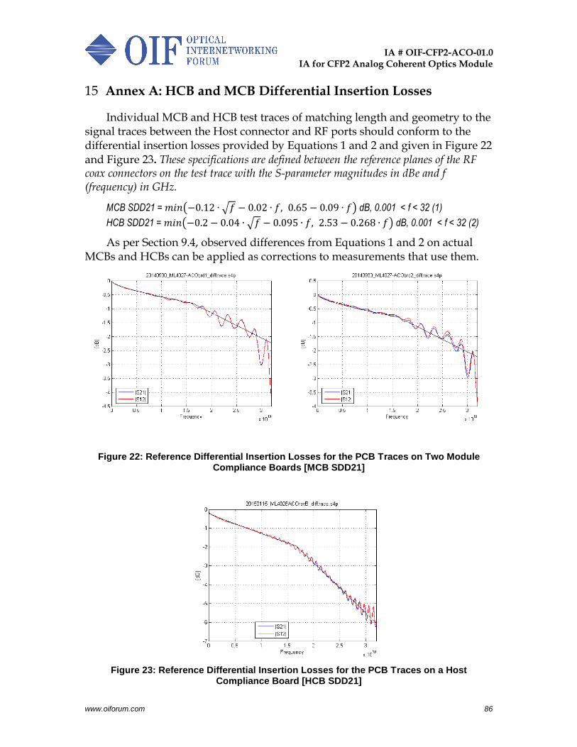
IA # OIF-CFP2-ACO-01.0
IA for CFP2 Analog Coherent Optics Module
www.oiforum.com 86
Annex A: HCB and MCB Differential Insertion Losses 15
Individual MCB and HCB test traces of matching length and geometry to the signal traces between the Host connector and RF ports should conform to the differential insertion losses provided by Equations 1 and 2 and given in Figure 22 and Figure 23. These specifications are defined between the reference planes of the RF coax connectors on the test trace with the S-parameter magnitudes in dBe and f (frequency) in GHz.
MCB SDD21 = 𝑚𝑖𝑛(−0.12 ∙ √𝑓 − 0.02 ∙ 𝑓, 0.65 − 0.09 ∙ 𝑓) dB, 0.001 < f < 32 (1)
HCB SDD21 = 𝑚𝑖𝑛(−0.2 − 0.04 ∙ √𝑓 − 0.095 ∙ 𝑓, 2.53 − 0.268 ∙ 𝑓) dB, 0.001 < f < 32 (2)
As per Section 9.4, observed differences from Equations 1 and 2 on actual MCBs and HCBs can be applied as corrections to measurements that use them.
Figure 22: Reference Differential Insertion Losses for the PCB Traces on Two Module Compliance Boards [MCB SDD21]
Figure 23: Reference Differential Insertion Losses for the PCB Traces on a Host Compliance Board [HCB SDD21]
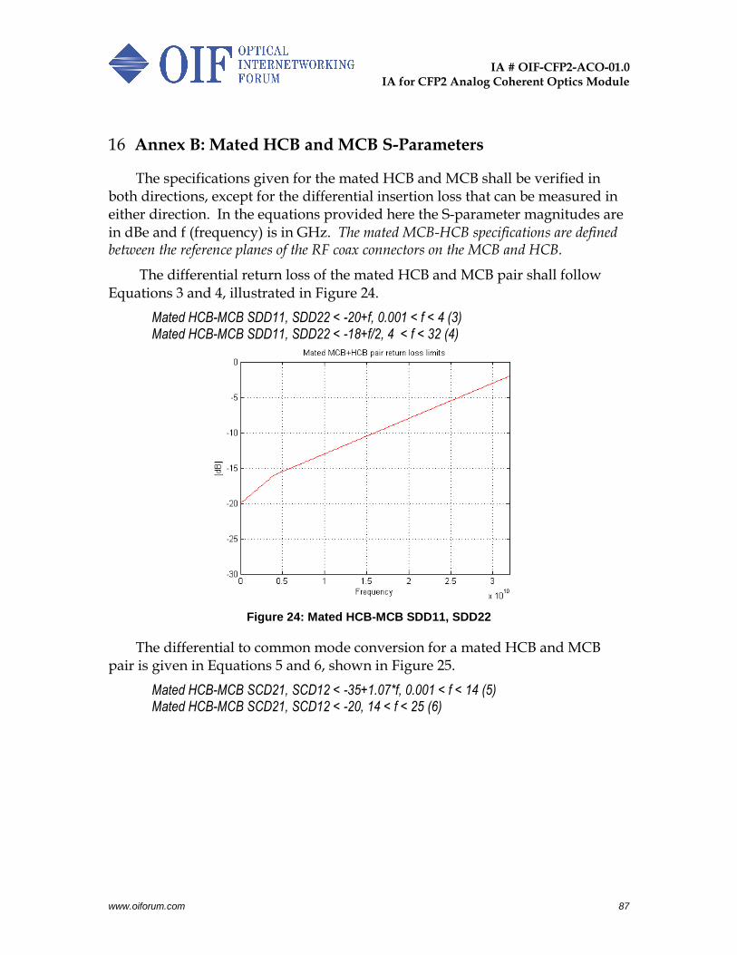
IA # OIF-CFP2-ACO-01.0
IA for CFP2 Analog Coherent Optics Module
www.oiforum.com 87
Annex B: Mated HCB and MCB S-Parameters 16
The specifications given for the mated HCB and MCB shall be verified in both directions, except for the differential insertion loss that can be measured in either direction. In the equations provided here the S-parameter magnitudes are in dBe and f (frequency) is in GHz. The mated MCB-HCB specifications are defined between the reference planes of the RF coax connectors on the MCB and HCB.
The differential return loss of the mated HCB and MCB pair shall follow Equations 3 and 4, illustrated in Figure 24.
Mated HCB-MCB SDD11, SDD22 < -20+f, 0.001 < f < 4 (3) Mated HCB-MCB SDD11, SDD22 < -18+f/2, 4 < f < 32 (4)
Figure 24: Mated HCB-MCB SDD11, SDD22
The differential to common mode conversion for a mated HCB and MCB pair is given in Equations 5 and 6, shown in Figure 25.
Mated HCB-MCB SCD21, SCD12 < -35+1.07*f, 0.001 < f < 14 (5) Mated HCB-MCB SCD21, SCD12 < -20, 14 < f < 25 (6)
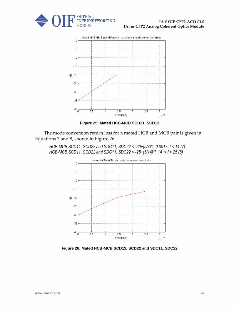
IA # OIF-CFP2-ACO-01.0
IA for CFP2 Analog Coherent Optics Module
www.oiforum.com 88
Figure 25: Mated HCB-MCB SCD21, SCD12
The mode conversion return loss for a mated HCB and MCB pair is given in Equations 7 and 8, shown in Figure 26.
HCB-MCB SCD11, SCD22 and SDC11, SDC22 < -30+(5/7)*f, 0.001 < f < 14 (7) HCB-MCB SCD11, SCD22 and SDC11, SDC22 < -25+(5/14)*f, 14 < f < 25 (8)
Figure 26: Mated HCB-MCB SCD11, SCD22 and SDC11, SDC22
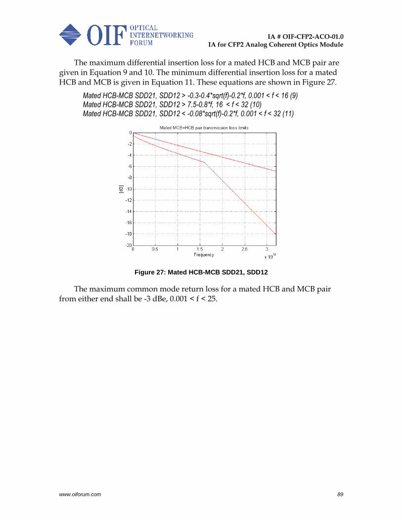
IA # OIF-CFP2-ACO-01.0
IA for CFP2 Analog Coherent Optics Module
www.oiforum.com 89
The maximum differential insertion loss for a mated HCB and MCB pair are given in Equation 9 and 10. The minimum differential insertion loss for a mated HCB and MCB is given in Equation 11. These equations are shown in Figure 27.
Mated HCB-MCB SDD21, SDD12 > -0.3-0.4*sqrt(f)-0.2*f, 0.001 < f < 16 (9) Mated HCB-MCB SDD21, SDD12 > 7.5-0.8*f, 16 < f < 32 (10) Mated HCB-MCB SDD21, SDD12 < -0.08*sqrt(f)-0.2*f, 0.001 < f < 32 (11)
Figure 27: Mated HCB-MCB SDD21, SDD12
The maximum common mode return loss for a mated HCB and MCB pair from either end shall be -3 dBe, 0.001 < f < 25.
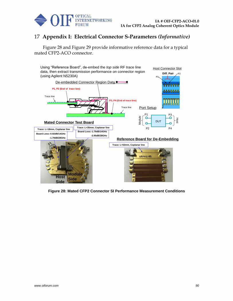
IA # OIF-CFP2-ACO-01.0
IA for CFP2 Analog Coherent Optics Module
www.oiforum.com 90
Appendix I: Electrical Connector S-Parameters (Informative) 17
Figure 28 and Figure 29 provide informative reference data for a typical mated CFP2-ACO connector.
Figure 28: Mated CFP2 Connector SI Performance Measurement Conditions
Using “Reference Board”, de-embed the top side RF trace line
data, then extract transmission performance on connector region
(using Agilent N5230A)
Port Setup
DUT
P1
P2
P3
P4
Mo
du
le Ho
st
Host Connector Slot
P1
P2
De-embedded Connector Region Data
P1, P2 (End of trace line)
P3, P4 (End of trace line)
Trace line
Trace line
Mated Connector Test Board
Trace: L=18mm, Coplanar lineBoard Loss:-1.79dB/14GHz
-2.95dB/28GHzBoard Loss:-0.92dB/14GHz
-1.79dB/28GHz
Trace: L=35mm, Coplanar line
Module
SideHost
Side
Reference Board for De-Embedding
Trace: L=53mm, Coplanar line
Diff. Pair
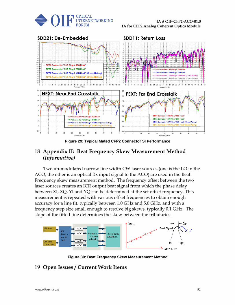
IA # OIF-CFP2-ACO-01.0
IA for CFP2 Analog Coherent Optics Module
www.oiforum.com 91
Figure 29: Typical Mated CFP2 Connector SI Performance
Appendix II: Beat Frequency Skew Measurement Method 18(Informative)
Two un-modulated narrow line width CW laser sources (one is the LO in the ACO, the other is an optical Rx input signal to the ACO) are used in the Beat Frequency skew measurement method. The frequency offset between the two laser sources creates an ICR output beat signal from which the phase delay between XI, XQ, YI and YQ can be determined at the set offset frequency. This measurement is repeated with various offset frequencies to obtain enough accuracy for a line fit, typically between 1.0 GHz and 5.0 GHz, and with a frequency step size small enough to resolve big skews, typically 0.1 GHz. The slope of the fitted line determines the skew between the tributaries.
Figure 30: Beat Frequency Skew Measurement Method
Open Issues / Current Work Items 19
IA # OIF-CFP2-ACO-01.0
IA for CFP2 Analog Coherent Optics Module
www.oiforum.com 92
List of Companies Belonging to OIF when Document is 20Approved
Acacia Communications Gigoptix O-Net Communications (HK) Limited
ADVA Optical Networking Global Foundries Oclaro
Alcatel-Lucent Google Orange
Altera Hitachi PETRA
AMCC Huawei Technologies Co., Ltd. Picometrix
Amphenol Corp. Infinera PMC Sierra
Analog Devices Inphi QLogic Corporation
Anritsu Intel Qorvo
Avago Technologies Inc. Ixia Rockley Photonics
Broadcom Juniper Networks Samtec Inc.
Brocade Kandou Bus Semtech
BTI Systems KDDI R&D Laboratories Socionext Inc.
China Telecom Keysight Technologies, Inc. Spirent Communications
Ciena Corporation Leaba Sumitomo Electric Industries
Cisco Systems Lumentum Sumitomo Osaka Cement
ClariPhy Communications Luxtera TE Connectivity
Compass Networks M/A-COM Technology Solutions
Tektronix
Coriant Marvell Technology TELUS Communications, Inc.
CPqD Mellanox Technologies TeraXion
EMC Corporation Microsemi Inc. Texas Instruments
Ericsson Microsoft Corporation Time Warner Cable
ETRI Mitsubishi Electric Corporation US Conec
FCI USA LLC Molex Verizon
Fiberhome Technologies Group
MoSys, Inc. Viavi Solutions Deutschland GmbH
Finisar Corporation NEC Xilinx
Fujikura NeoPhotonics Yamaichi Electronics Ltd.
Fujitsu NTT Corporation ZTE Corporation
Furukawa Electric Japan