Embed Size (px)
Citation preview
AN721
1RF Application InformationFreescale Semiconductor
Impedance Matching NetworksApplied to RF Power TransistorsBy: B. Becciolini
1. INTRODUCTION
Some graphic and numerical methods of impedancematching will be reviewed here. The examples given will referto high frequency power amplifiers.
Although matching networks normally take the form offilters and therefore are also useful to provide frequencydiscrimination, this aspect will only be considered as acorollary of the matching circuit.
Matching is necessary for the best possible energytransfer from stage to stage. In RF-power transistors theinput impedance is of low value, decreasing as the powerincreases, or as the chip size becomes larger. Thisimpedance must be matched either to a generator — ofgenerally 50 ohms internal impedance — or to a precedingstage. Impedance transformation ratios of 10 or even 20 arenot rare. Interstage matching has to be made between twocomplex impedances, which makes the design still moredifficult, especially if matching must be accomplished overa wide frequency band.
2. DEVICE PARAMETERS
2.1 INPUT IMPEDANCE
The general shape of the input impedance of RF-powertransistors is as shown in Figure 1. It is a large signalparameter, expressed here by the parallel combination ofa resistance Rp and a reactance Xp (Ref. (1)).
The equivalent circuit shown in Figure 2 accounts for thebehavior illustrated in Figure 1.
With the presently used stripline or flange packaging,most of the power devices for VHF low band will have theirRp and Xp values below the series resonant point fs. Theinput impedance will be essentially capacitive.
Most of the VHF high band transistors will have the seriesresonant frequency within their operating range, i.e. bepurely resistive at one single frequency fs, while the parallelresonant frequency fp will be outside.
Parameters for one or two gigahertz transistors will bebeyond fs and approach fp. They show a high value of Rpand Xp with inductive character.
A parameter that is very often used to judge on thebroadband capabilities of a device is the input Q or QlNdefined simply as the ratio Rp/Xp. Practically QlN rangesaround 1 or less for VHF devices and around 5 or more formicrowave transistors.
Rp
fS fPf
f
fS fP
XP
IND.
CAP.
Figure 1. Input Impedance of RF-Power Transistors asa Function of Frequency
ZIN CTECDECC
LS RBB
RE
Where:RE = emitter diffusion resistanceCDE,CTE = diffusion and transition capacitances of the
emitter junctionRBB = base spreading resistanceCC = package capacitanceLS = base lead inductance
Figure 2. Equivalent Circuit for the Input Impedance ofRF-Power Transistors
QIN is an important parameter to consider for broadbandmatching. Matching networks normally are low-pass orpseudo low-pass filters. If QlN is high, it can be necessaryto use band-pass filter type matching networks and to allowinsertion losses. But broadband matching is still possible.This will be discussed later.
2.2 OUTPUT IMPEDANCE
The output impedance of the RF-power transistors, asgiven by all manufacturers’ data sheets, generally consistsof only a capacitance COUT. The internal resistance of thetransistor is supposed to be much higher than the load andis normally neglected. In the case of a relatively low internalresistance, the efficiency of the device would decrease bythe factor:
1 + RL/RT
AN721Rev. 1.1, 10/2005
Freescale SemiconductorApplication Note
NOTE: The theory in this application note is still applicable,but some of the products referenced may be discontinued.
Freescale Semiconductor, Inc., 1993, 2005, 2009. All rights reserved.
2RF Application InformationFreescale Semiconductor
AN721
where RL is the load resistance, seen at the collector-emitterterminals, and RT the internal transistor resistance equal to:
,1
T, (CTC + CDC)
defined as a small signal parameter, where:
T = transit angular frequencyCTC + CDC = transition and diffusion capacitances
at the collector junction
The output capacitance COUT, which is a large signalparameter, is related to the small signal parameter CCB, thecollector-base transition capacitance.
Since a junction capacitance varies with the appliedvoltage, COUT differs from CCB in that it has to be averagedover the total voltage swing. For an abrupt junction andassuming certain simplifications, COUT = 2 CCB.
Figure 3 shows the variation of COUT with frequency.COUT decreases partly due to the presence of the collectorlead inductance, but mainly because of the fact that thebase-emitter diode does not shut off anymore when theoperating frequency approaches the transit frequency fT.
f
COUT
Figure 3. Output Capacitance COUT as a Functionof Frequency
3. OUTPUT LOAD
In the absence of a more precise indication, the outputload RL is taken equal to:
RL =2POUT
[VCC -- VCE(sat)]2
with VCE(sat) equal to 2 or 3 volts, increasing with frequency.The above equation just expresses a well-known relation,
but also shows that the load, in first approximation, is notrelated to the device, except for VCE(sat). The load valueis primarily dictated by the required output power and thepeak voltage; it is not matched to the output impedance ofthe device.
At higher frequencies this approximation becomes lessexact and for microwave devices the load that must bepresented to the device is indicated on the data sheet. Thisparameter will be measured on all Freescale RF-powerdevices in the future.
Strictly speaking, impedance matching is accomplishedonly at the input. Interstage and load matching are moreimpedance transformations of the device input impedanceand of the load into a value RL (sometimes with additionalreactive component) that depends essentially on the powerdemanded and the supply voltage.
4. MATCHING NETWORKS
In the following matching networks will be described byorder of complexity. These are ladder type reactancenetworks.
The different reactance values will be calculated anddetermined graphically. Increasing the number of reactancesbroadens the bandwidth. However, networks consisting ofmore than four reactances are rare. Above four reactances,the improvement is small.
4.1 NUMERICAL DESIGN
4.1.1 Two-Resistance Networks
Resistance terminations will first be considered. Figure 4shows the reactive L-section and the terminations to bematched.
X2
R2 =R1n
n > 1
X1R1
Figure 4. Two-Reactance Matching Network
Matching or exact transformation from R2 into R1 occursat a single frequency fo.
At fo, X1 and X2 are equal to:
X1 = R1R1 -- R2
R2= R1
1
n -- 1
X2 = R2 (R1 -- R2) = R11
n -- 1
At fo: X1 X2 = R1 R2
X1 and X2 must be of opposite sign. The shunt reactance isin parallel with the larger resistance.
The frequency response of the L-section is shown inFigure 5, where the normalized current is plotted as afunction of the normalized frequency.
I2Io
1.0
0.8
0.6
0.4
0.5 0.7 0.9 1.1 1.3 1.5f/fo LOW-PASS — fo/f HIGH-PASS
Qo = 1
Qo = 2
Qo = 3
2456810
2
456810
X1I2
X2R1
E
Qo = n -- 1
n = R1/R2
R2
Figure 5. Normalized Frequency Response for theL-Section in Low-Pass or High-Pass Form
AN721
3RF Application InformationFreescale Semiconductor
If X1 is capacitive and consequently X2 inductive, then:
X1 = --R1 -- R2
R2= --
1
n -- 1f
foR1
f
foR1
and X2 =1
n -- 1R2 (R1 -- R2) =
fo
f
fo
fR1
The normalized current absolute value is equal to:
=2 n
(n -- 1)2 fo
f 4 -- 2fo
f 2 + (n + 1)2Io
I2
where Io = 2 R1
nE, and is plotted in Figure 5 (Ref. (2)).
If X1 is inductive and consequently X2 capacitive, the onlychange required is a replacement of f by fo and vice-versa.The L-section has low pass form in the first case andhigh-pass form in the second case.
The Q of the circuit at fo is equal to:
Qo =X1
R1= n -- 1
R2
X2=
For a given transformation ratio n, there is only onepossible value of Q. On the other hand, there are twosymmetrical solutions for the network, that can be either alow-pass filter or a high-pass filter.
The frequency fo does not need to be the centerfrequency, (f1 + f2)/2, of the desired band limited by f1and f2.
In fact, as can be seen from the low-pass configurationof Figure 5, it may be interesting to shift fo toward the highband edge frequency f2 to obtain a larger bandwidth w, where
w =f2 -- f1
2 (f1 + f2)
This will, however, be at the expense of poorer harmonicrejection.
Example:
For a transformation ratio n = 4, it can be determined fromthe above relations:
Bandwidth w 0.1 0.3Max insertion losses 0.025 0.2X1/R1 1.730 1.712
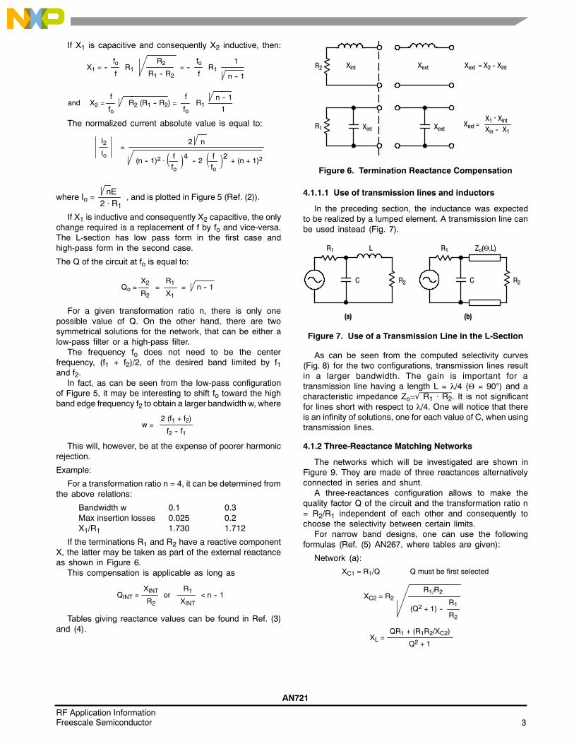
If the terminations R1 and R2 have a reactive componentX, the latter may be taken as part of the external reactanceas shown in Figure 6.
This compensation is applicable as long as
QINT =XINT
R1< n -- 1
R2
XINTor
Tables giving reactance values can be found in Ref. (3)and (4).
XintR2
R1
Xext
Xint Xext
Xext = X2 -- Xint
Xext =X1 XintXin -- X1
Figure 6. Termination Reactance Compensation
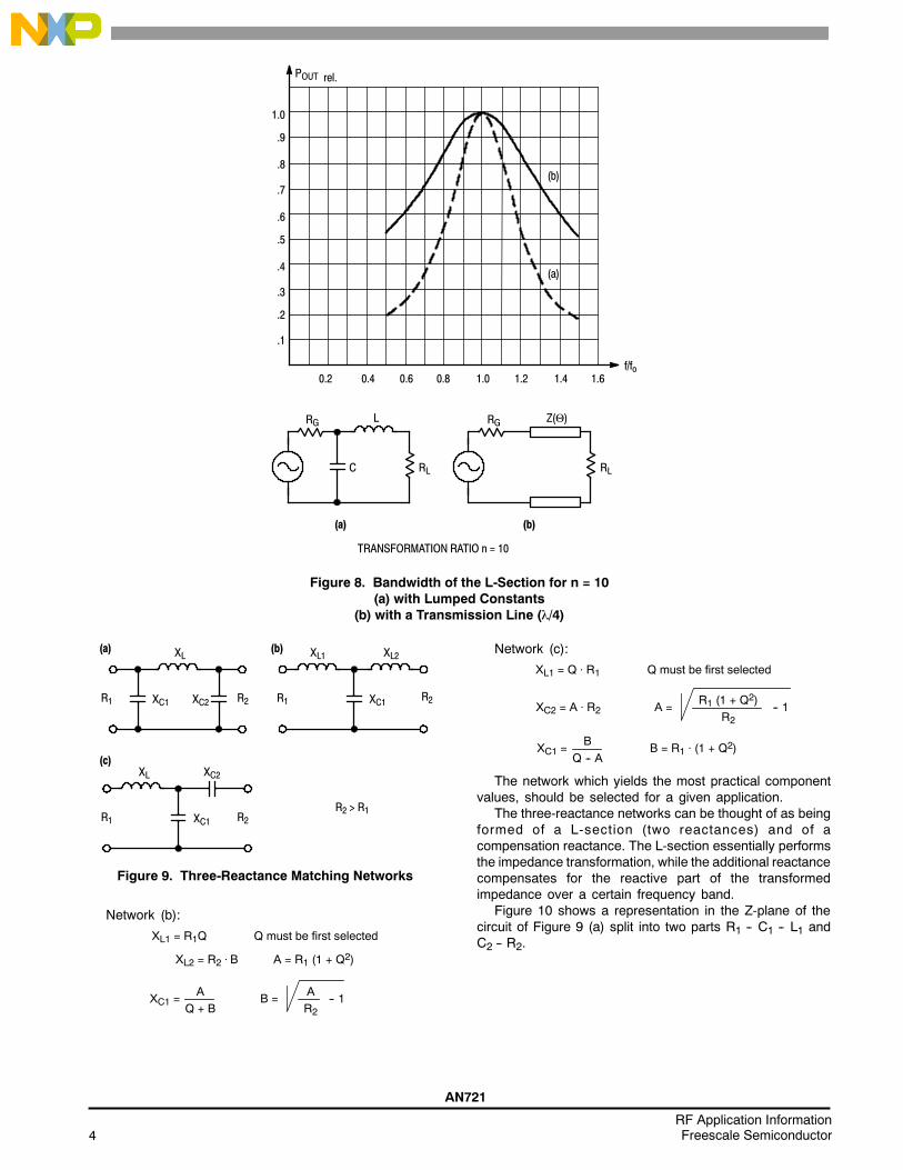
4.1.1.1 Use of transmission lines and inductors
In the preceding section, the inductance was expectedto be realized by a lumped element. A transmission line canbe used instead (Fig. 7).
R2
R1 Zo(,L)
C
R1
C
L
R2
(a) (b)
Figure 7. Use of a Transmission Line in the L-Section
As can be seen from the computed selectivity curves(Fig. 8) for the two configurations, transmission lines resultin a larger bandwidth. The gain is important for atransmission line having a length L = /4 ( = 90) and acharacteristic impedance Zo= R1 R2. It is not significantfor lines short with respect to /4. One will notice that thereis an infinity of solutions, one for each value of C, when usingtransmission lines.
4.1.2 Three-Reactance Matching Networks
The networks which will be investigated are shown inFigure 9. They are made of three reactances alternativelyconnected in series and shunt.
A three-reactances configuration allows to make thequality factor Q of the circuit and the transformation ratio n= R2/R1 independent of each other and consequently tochoose the selectivity between certain limits.
For narrow band designs, one can use the followingformulas (Ref. (5) AN267, where tables are given):
Network (a):
XC1 = R1/Q Q must be first selected
XC2 = R2
(Q2 + 1) --
R1/R2
R2
R1
XL =Q2 + 1
QR1 + (R1R2/XC2)
4RF Application InformationFreescale Semiconductor
AN721
RL
RG Z()RG
C
L
RL
(a) (b)
1.0
.9
.8
.7
0.2 0.4 0.6 0.8 1.0
(a)
(b)
f/fo
.6
.5
.4
.3
.2
.1
1.2 1.4 1.6
POUT rel.
TRANSFORMATION RATIO n = 10
Figure 8. Bandwidth of the L-Section for n = 10(a) with Lumped Constants
(b) with a Transmission Line (/4)
XL
R1 XC1 R1 XC1R2XC2 R2
XL1 XL2
R1 XC1
XL XC2
R2 > R1
(a) (b)
(c)
R2
Figure 9. Three-Reactance Matching Networks
Network (b):
XL1 = R1Q Q must be first selected
XL2 = R2 B A = R1 (1 + Q2)
XC1 =R2
AQ + BA
-- 1B =
Network (c):
XL1 = Q R1 Q must be first selected
R2
R1 (1 + Q2)-- 1A =XC2 = A R2
XC1 =Q -- AB
B = R1 (1 + Q2)
The network which yields the most practical componentvalues, should be selected for a given application.
The three-reactance networks can be thought of as beingformed of a L-section (two reactances) and of acompensation reactance. The L-section essentially performsthe impedance transformation, while the additional reactancecompensates for the reactive part of the transformedimpedance over a certain frequency band.
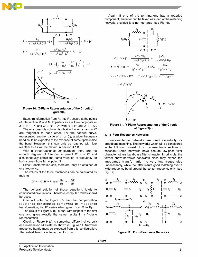
Figure 10 shows a representation in the Z-plane of thecircuit of Figure 9 (a) split into two parts R1 -- C1 -- L1 andC2 -- R2.
AN721
5RF Application InformationFreescale Semiconductor
L1
R1 C1 R2C2
Z =R1
1 + 2 R12 C12+ j
R12C11 + 2 R12 C12
L1 --
Z =R2
1 + 2 C22 R22--1 + 2 C22 R22
= R + jXj2 C2 R22
C1 R12 x =
L1--R1
R -- 1R
R1
x = R R2 -- R2x, -- x
x
M--x
M
N
R2 R1R
= R + jX
Z Z
Figure 10. Z-Plane Representation of the Circuit ofFigure 9(a)
Exact transformation from R1 into R2 occurs at the pointsof intersection M and N. Impedances are then conjugate orZ = R + jX and Z = R + jX with R = R and X = -- X.
The only possible solution is obtained when X and -- Xare tangential to each other. For the dashed curve,representing another value of L1 or C1, a wider frequencyband could be expected at the expense of some ripple insidethe band. However, this can only be reached with fourreactances as will be shown in section 4.1.3.
With a three-reactance configuration, there are notenough degrees of freedom to permit X = -- X andsimultaneously obtain the same variation of frequency onboth curves from M to point N.
Exact transformation can, therefore, only be obtained atone frequency.
The values of the three reactances can be calculated bymaking
dRdX
X = -- X, R = R and = --dRdX
.
The general solution of these equations leads tocomplicated calculations. Therefore, computed tables shouldbe used.
One will note on Figure 10 that the compensationreac tance cont r ibu tes somewhat to impedancetransformation, i.e. R varies when going from M to R2.
The circuit of Figure 9 (b) is dual with respect to the firstone and gives exactly the same results in a Y-planerepresentation.
Circuit of Figure 9 (c) is somewhat different since onlyone intersection M exists as shown in Figure 11. Narrowerfrequency bands must be expected from this configuration.The widest band is obtained for C1 = .
Again, if one of the terminations has a reactivecomponent, the latter can be taken as a part of the matchingnetwork, provided it is not too large (see Fig. 6).
L2
R2(G2) C2
Y = G + jB =2C12R1
1 + 2 C12 R12--
jC11 + 2 C12 R12
R1(G1)
Y = G + jB =R2
R22 + 2L22+ jC2 --
jL2
R22 + 2L22
Y Y
B = -- G/R1 -- G2 B = (1/kR2 -- G) 1/GR2 -- 1
k =L2/C2R22
B
G1
BM
G2G or G
(f1)
C1
B .-- B
Figure 11. Y-Plane Representation of the Circuitof Figure 9(c)
4.1.3 Four-Reactance Networks
Four-reactance networks are used essentially forbroadband matching. The networks which will be consideredin the following consist of two two-reactance sections incascade. Some networks have pseudo low-pass filtercharacter, others band-pass filter character. In principle, theformer show narrower bandwidth since they extend theimpedance transformation to very low frequenciesunnecessarily, while the latter insure good matching over awide frequency band around the center frequency only (seeFig. 14).
Z1 Z2
X1R1 X4 R2
X2 X3M
X1R1 X3 R2
X2 X4M
X1R1 X3R2
X2 M
R1 X3 R2
X2 X4MX1
R1 = n.R2
c)
a) b)
d)
X4
Figure 12. Four-Reactance Networks
6RF Application InformationFreescale Semiconductor
AN721
The two-reactance sections used in above networks haveeither transformation properties or compensation properties.Impedance transformation is obtained with one seriesreactance and one shunt reactance. Compensation is madewith both reactances in series or in shunt.
If two cascaded transformation networks are used,transformation is accomplished partly by each one.
With four-reactance networks there are two frequencies,f1 and f2, at which the transformation from R1 into R2 is exact.These frequencies may also coincide.
For network (b) for instance, at point M, R1 or R2 istransformed into R1R2 when both frequencies fall together.At all points (M), Z1 and Z2 are conjugate if the transformationis exact.
In the case of Figure 12 (b) the reactances are easily,calculated for equal frequencies:
X1 =R1
, X2 = R1n
n -- 1
n -- 1
X1 X4 = R1 R2 = X2 X3
X3 =R1
n ( n -- 1)
, X4 =n
R1n -- 1
For network (a) normally, at point (M), Z1 and Z2 arecomplex. This pseudo low-pass filter has been computedelsewhere (Ref. (3)). Many tables can be found in theliterature for networks of four and more reactances havingTchebyscheff character or maximally-flat response (Ref. (3),(4) and (6)).
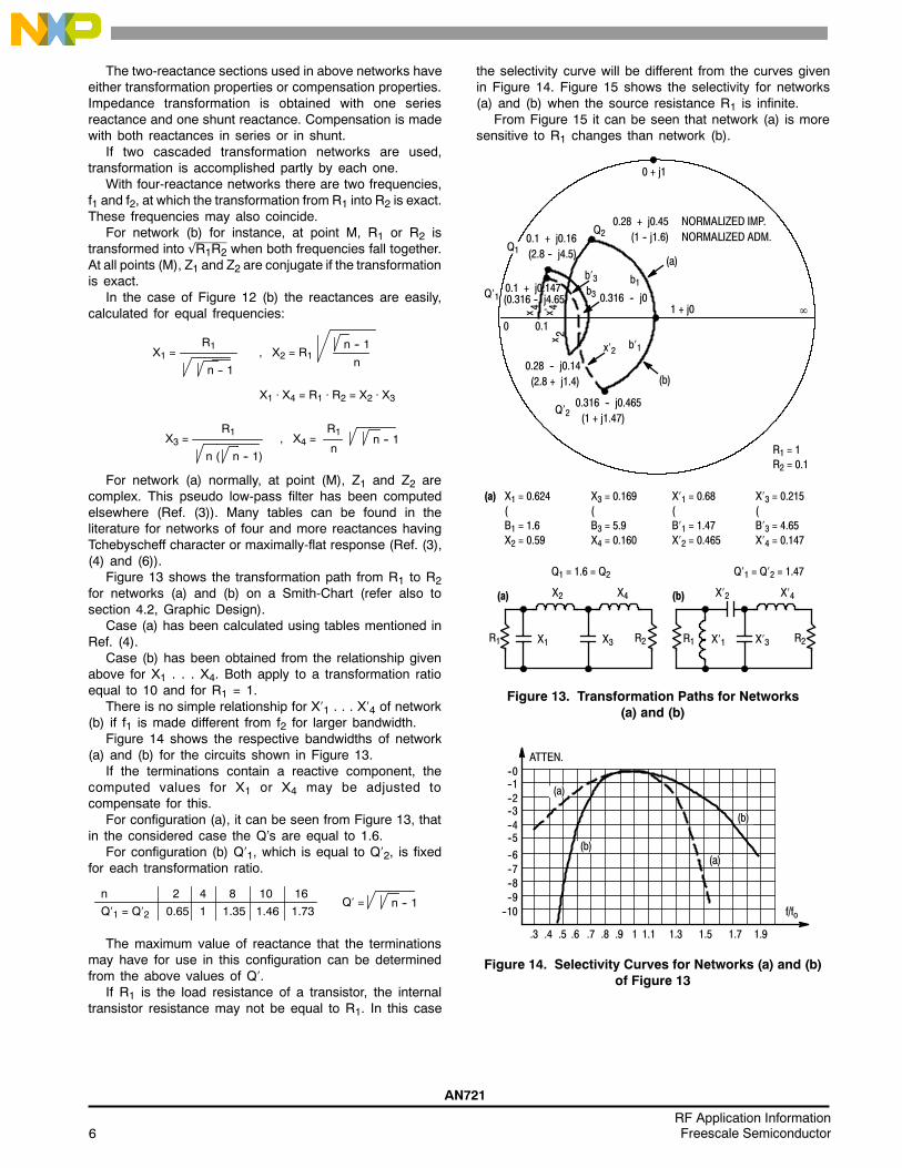
Figure 13 shows the transformation path from R1 to R2for networks (a) and (b) on a Smith-Chart (refer also tosection 4.2, Graphic Design).
Case (a) has been calculated using tables mentioned inRef. (4).
Case (b) has been obtained from the relationship givenabove for X1 . . . X4. Both apply to a transformation ratioequal to 10 and for R1 = 1.
There is no simple relationship for X1 . . . X4 of network(b) if f1 is made different from f2 for larger bandwidth.
Figure 14 shows the respective bandwidths of network(a) and (b) for the circuits shown in Figure 13.
If the terminations contain a reactive component, thecomputed values for X1 or X4 may be adjusted tocompensate for this.
For configuration (a), it can be seen from Figure 13, thatin the considered case the Q’s are equal to 1.6.
For configuration (b) Q1, which is equal to Q2, is fixedfor each transformation ratio.
Q = n -- 1n 2 4 8 10 16
Q1 = Q2 0.65 1 1.35 1.46 1.73
The maximum value of reactance that the terminationsmay have for use in this configuration can be determinedfrom the above values of Q.
If R1 is the load resistance of a transistor, the internaltransistor resistance may not be equal to R1. In this case
the selectivity curve will be different from the curves givenin Figure 14. Figure 15 shows the selectivity for networks(a) and (b) when the source resistance R1 is infinite.
From Figure 15 it can be seen that network (a) is moresensitive to R1 changes than network (b).
X2
R1 X1 R2X3
X4 X2
R1 X1 X3
X4
R2
0 + j1
0.28 + j0.45 NORMALIZED IMP.(1 -- j1.6) NORMALIZED ADM.
Q20.1 + j0.16(2.8 -- j4.5)
0.1 + j0.147(0.316 -- j4.65)Q1
0.316 -- j0.465(1 + j1.47)
Q2
0.28 -- j0.14(2.8 + j1.4)
0 0.11 + j0
(b)
(a)
b1
b1
0.316 -- j0
x x’ 44
x 2
X1 = 0.624(B1 = 1.6X2 = 0.59
X3 = 0.169(B3 = 5.9X4 = 0.160
X1 = 0.68(B1 = 1.47X2 = 0.465
X3 = 0.215(B3 = 4.65X4 = 0.147
R1 = 1R2 = 0.1
Q1 = 1.6 = Q2 Q1 = Q2 = 1.47
(a) (b)
Q1
b3
b3
x2
(a)
Figure 13. Transformation Paths for Networks(a) and (b)
--10--9--8
.3
f/fo
--6
--4--3--2--1
ATTEN.--0
.4 .5 .6 .7 .8 .9 1 1.1 1.3 1.5 1.7 1.9
(a)
(a)(b)
--5
--7
(b)
Figure 14. Selectivity Curves for Networks (a) and (b)of Figure 13
AN721
7RF Application InformationFreescale Semiconductor
--10--9--8--7
f/fo
--6--5--4--3--2--1
REL. ATTEN.
0
.4 .5 .6 .7 .8 .9 1 1.1 1.3 1.5 1.7
12
(a) (a) (b)(b)
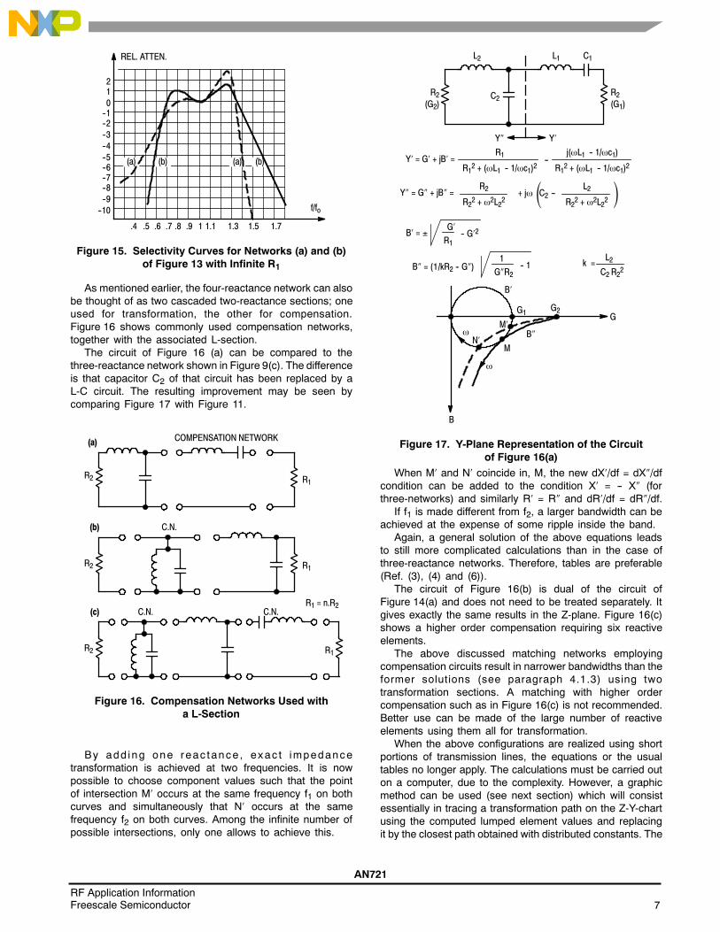
Figure 15. Selectivity Curves for Networks (a) and (b)of Figure 13 with Infinite R1
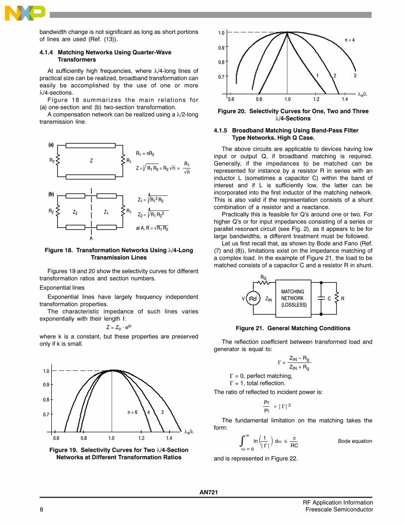
As mentioned earlier, the four-reactance network can alsobe thought of as two cascaded two-reactance sections; oneused for transformation, the other for compensation.Figure 16 shows commonly used compensation networks,together with the associated L-section.
The circuit of Figure 16 (a) can be compared to thethree-reactance network shown in Figure 9(c). The differenceis that capacitor C2 of that circuit has been replaced by aL-C circuit. The resulting improvement may be seen bycomparing Figure 17 with Figure 11.
R2
(a)
R1
COMPENSATION NETWORK
R1
(b) C.N.
R2
R1
(c) C.N.
R2
C.N.R1 = n.R2
Figure 16. Compensation Networks Used witha L-Section
By add ing one reac tance , exac t impedancetransformation is achieved at two frequencies. It is nowpossible to choose component values such that the pointof intersection M occurs at the same frequency f1 on bothcurves and simultaneously that N occurs at the samefrequency f2 on both curves. Among the infinite number ofpossible intersections, only one allows to achieve this.
R2(G2)
R2(G1)
Y Y
L2 L1 C1
Y = G + jB =R1
R12 + (L1 -- 1/c1)2--
C2 R22k =
L2
-- G2R1
G
R12 + (L1 -- 1/c1)2j(L1 -- 1/c1)
Y = G + jB =R2
R22 + 2L22+ j C2 --
L2
R22 + 2L22
B =
B = (1/kR2 -- G) -- 1GR2
1
B
G1
B
M
G2G
B
N
M
C2
Figure 17. Y-Plane Representation of the Circuitof Figure 16(a)
When M and N coincide in, M, the new dX/df = dX/dfcondition can be added to the condition X = -- X (forthree-networks) and similarly R = R and dR/df = dR/df.
If f1 is made different from f2, a larger bandwidth can beachieved at the expense of some ripple inside the band.
Again, a general solution of the above equations leadsto still more complicated calculations than in the case ofthree-reactance networks. Therefore, tables are preferable(Ref. (3), (4) and (6)).
The circuit of Figure 16(b) is dual of the circuit ofFigure 14(a) and does not need to be treated separately. Itgives exactly the same results in the Z-plane. Figure 16(c)shows a higher order compensation requiring six reactiveelements.
The above discussed matching networks employingcompensation circuits result in narrower bandwidths than theformer solutions (see paragraph 4.1.3) using twotransformation sections. A matching with higher ordercompensation such as in Figure 16(c) is not recommended.Better use can be made of the large number of reactiveelements using them all for transformation.
When the above configurations are realized using shortportions of transmission lines, the equations or the usualtables no longer apply. The calculations must be carried outon a computer, due to the complexity. However, a graphicmethod can be used (see next section) which will consistessentially in tracing a transformation path on the Z-Y-chartusing the computed lumped element values and replacingit by the closest path obtained with distributed constants. The
8RF Application InformationFreescale Semiconductor
AN721
bandwidth change is not significant as long as short portionsof lines are used (Ref. (13)).
4.1.4 Matching Networks Using Quarter-WaveTransformers
At sufficiently high frequencies, where /4-long lines ofpractical size can be realized, broadband transformation caneasily be accomplished by the use of one or more/4-sections.
Figure 18 summarizes the main relat ions for(a) one-section and (b) two-section transformation.
A compensation network can be realized using a /2-longtransmission line.
R1 nR2Z
Z = R1 R2 = R2 n =R1R2
A
R1R2
n
R1
(a)
Z1 = R13 R2
Z2 = R1 R23
at A, R = R1 R2
Z2 Z1
(b) 4
4
Figure 18. Transformation Networks Using /4-LongTransmission Lines
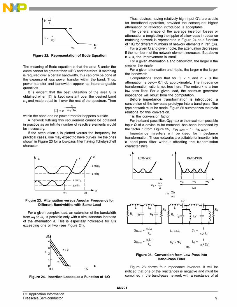
Figures 19 and 20 show the selectivity curves for differenttransformation ratios and section numbers.
Exponential lines
Exponential lines have largely frequency independenttransformation properties.
The characteristic impedance of such lines variesexponentially with their length I:
Z = Zo ekl
where k is a constant, but these properties are preservedonly if k is small.
0.9
0.8
0.7 24
0.6 0.8 1.0 1.2 1.4
1.0
n = 6
o/
Figure 19. Selectivity Curves for Two /4-SectionNetworks at Different Transformation Ratios
0.9
0.8
0.7 32
0.6 0.8 1.0 1.2 1.4
1.0n = 4
o/
1
Figure 20. Selectivity Curves for One, Two and Three/4-Sections
4.1.5 Broadband Matching Using Band-Pass FilterType Networks. High Q Case.
The above circuits are applicable to devices having lowinput or output Q, if broadband matching is required.Generally, if the impedances to be matched can berepresented for instance by a resistor R in series with aninductor L (sometimes a capacitor C) within the band ofinterest and if L is sufficiently low, the latter can beincorporated into the first inductor of the matching network.This is also valid if the representation consists of a shuntcombination of a resistor and a reactance.
Practically this is feasible for Q’s around one or two. Forhigher Q’s or for input impedances consisting of a series orparallel resonant circuit (see Fig. 2), as it appears to be forlarge bandwidths, a different treatment must be followed.
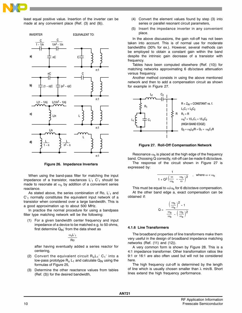
Let us first recall that, as shown by Bode and Fano (Ref.(7) and (8)), limitations exist on the impedance matching ofa complex load. In the example of Figure 21, the load to bematched consists of a capacitor C and a resistor R in shunt.
R
RG
CZIN
MATCHINGNETWORK(LOSSLESS)
V
Figure 21. General Matching Conditions
The reflection coefficient between transformed load andgenerator is equal to:
=ZIN + Rg
ZIN -- Rg
= 0, perfect matching, = 1, total reflection.
The ratio of reflected to incident power is:
= 2Pi
Pr
The fundamental limitation on the matching takes theform:
d≤
1ln
RC
= o
Bode equation
and is represented in Figure 22.
AN721
9RF Application InformationFreescale Semiconductor
c
1
ln
RC
S =
Figure 22. Representation of Bode Equation
The meaning of Bode equation is that the area S under thecurve cannot be greater than /RC and therefore, if matchingis required over a certain bandwidth, this can only be done atthe expense of less power transfer within the band. Thus,power transfer and bandwidth appear as interchangeablequantities.
It is evident that the best utilization of the area S isobtained when is kept constant over the desired bandc and made equal to 1 over the rest of the spectrum. Then
= e c RC
--
within the band and no power transfer happens outside.A network fulfilling this requirement cannot be obtained
in practice as an infinite number of reactive elements wouldbe necessary.
If the attenuation a is plotted versus the frequency forpractical cases, one may expect to have curves like the onesshown in Figure 23 for a low-pass filter having Tchebyscheffcharacter.
2
a
1
12
a max2
a min2
a max1a min1
Figure 23. Attenuation versus Angular Frequency forDifferent Bandwidths with Same Load
For a given complex load, an extension of the bandwidthfrom 1 to 2 is possible only with a simultaneous increaseof the attenuation a. This is especially noticeable for Q’sexceeding one or two (see Figure 24).
a
1
n = 22
3
4
0
3
1 1/Q0.1
dB
Figure 24. Insertion Losses as a Function of 1/Q
Thus, devices having relatively high input Q’s are usablefor broadband operation, provided the consequent higherattenuation or reflection introduced is acceptable.
The general shape of the average insertion losses orattenuation a (neglecting the ripple) of a low-pass impedancematching network is represented in Figure 24 as a functionof 1/Q for different numbers of network elements n (ref. (3)).
For a given Q and given ripple, the attenuation decreasesif the number n of the network element increases. But aboven = 4, the improvement is small.
For a given attenuation a and bandwidth, the larger n thesmaller the ripple.
For a given attenuation and ripple, the larger n the largerthe bandwidth.
Computations show that for Q < 1 and n 3 theattenuation is below 0.1 db approximately. The impedancetransformation ratio is not free here. The network is a truelow-pass filter. For a given load, the optimum generatorimpedance will result from the computation.
Before impedance transformation is introduced, aconversion of the low-pass prototype into a band-pass filtertype network must be made. Figure 25 summarizes the mainrelations for this conversion.
r is the conversion factor.For the band-pass filter, QlN max or the maximum possible
input Q of a device to be matched, has been increased bythe factor r (from Figure 25, QIN max = r QIN max).
Impedance inverters will be used for impedancetransformation. These networks are suitable for insertion intoa band-pass filter without affecting the transmissioncharacteristics.
Ro
a
wc =
LOW-PASS BAND-PASS
oa b
R5
2
r =o
a
L1 L3
C2 C4 Ro
R5L1
C2 L2
C1
QIN max =cL1Ro
L1 = r.L1 C1 =1
o2 L1
QIN max =oL1
RoC2 = r.C2 L2 =
1
o2 C2etc.
Figure 25. Conversion from Low-Pass intoBand-Pass Filter
Figure 26 shows four impedance inverters. It will benoticed that one of the reactances is negative and must becombined in the band-pass network with a reactance of at
10RF Application InformationFreescale Semiconductor
AN721
least equal positive value. Insertion of the inverter can bemade at any convenient place (Ref. (3) and (9)).
a)
n:1
nC C
b)
C
(1 -- n)C (n2 -- n)C
n:1
INVERTER EQUIVALENT TO:
c)L
n:1
L(1 -- 1/n) L(1/n2 -- 1/n)
L/n
d)
L
n:1
L1 -- n
Ln2 -- n
C1 -- 1/n
C1/n2 -- 1/n
L/n
nC
Figure 26. Impedance Inverters
When using the band-pass filter for matching the inputimpedance of a transistor, reactances L1 C1 should bemade to resonate at o by addition of a convenient seriesreactance.
As stated above, the series combination of Ro, L1 andC1 normally constitutes the equivalent input network of atransistor when considered over a large bandwidth. This isa good approximation up to about 500 MHz.
In practice the normal procedure for using a bandpassfilter type matching network will be the following:
(1) For a given bandwidth center frequency and inputimpedance of a device to be matched e.g. to 50 ohms,first determine QlN from the data sheet as
Ro
oL1
after having eventually added a series reactor forcentering,
(2) Convert the equivalent circuit RoL1 C1 into alow-pass prototype Ro L1 and calculate QlN using theformulas of Figure 25,
(3) Determine the other reactance values from tables(Ref. (3)) for the desired bandwidth,
(4) Convert the element values found by step (3) intoseries or parallel resonant circuit parameters,
(5) Insert the impedance inverter in any convenientplace.
In the above discussions, the gain roll-off has not beentaken into account. This is of normal use for moderatebandwidths (30% for ex.). However, several methods canbe employed to obtain a constant gain within the banddespite the intrinsic gain decrease of a transistor withfrequency.
Tables have been computed elsewhere (Ref. (10)) formatching networks approximating 6 db/octave attenuationversus frequency.
Another method consists in using the above mentionednetwork and then to add a compensation circuit as shownfor example in Figure 27.
R
L1 C1
L2 C2
R1R = ZIN = CONSTANT vs. f.
L1C1 = L2C2R1 = R
b2 = 1/L1C1 = 1/L2C2(HIGH BAND EDGE)
Q2 = bL2/R = Q1 = bC1R
Figure 27. Roll-Off Compensation Network
Resonance b is placed at the high edge of the frequencyband. Choosing Q correctly, roll-off can be made 6 db/octave.
The response of the circuit shown in Figure 27 isexpressed by:
1 + Q2
1
b
b
--2
, where < b
This must be equal to /b for 6 db/octave compensation.At the other band edge a, exact compensation can be
obtained if:
Q =ab
ba
--2
-- 1 ba2
4.1.6 Line Transformers
The broadband properties of line transformers make themvery useful in the design of broadband impedance matchingnetworks (Ref. (11) and (12)).
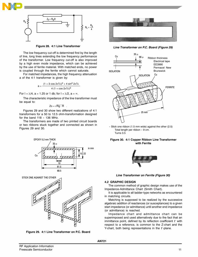
A very common form is shown by Figure 28. This is a4:1 impedance transformer. Other transformation ratios like9:1 or 16:1 are also often used but will not be consideredhere.
The high frequency cut-off is determined by the lengthof line which is usually chosen smaller than min/8. Shortlines extend the high frequency performance.
AN721
11RF Application InformationFreescale Semiconductor
RgZ0 = Rg/2
RL =Rg4
Figure 28. 4:1 Line Transformer
The low frequency cut-off is determined first by the lengthof line, long lines extending the low frequency performanceof the transformer. Low frequency cut-off is also improvedby a high even mode impedance, which can be achievedby the use of ferrite material. With matched ends, no poweris coupled through the ferrite which cannot saturate.
For matched impedances, the high frequency attenuationa of the 4:1 transformer is given by:
a =4 (1 + cos 2I/)2
(1 + 3 cos 2I/)2 + 4 sin2 2I/
For I = /4, a = 1.25 or 1 db; for I = /2, a = .
The characteristic impedance of the line transformer mustbe equal to:
Zo = Rg R .
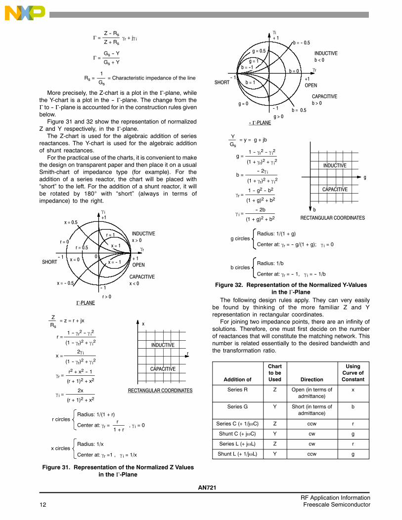
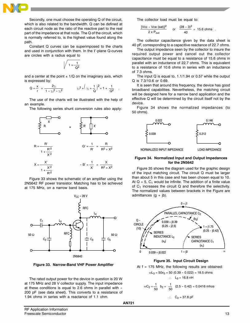
Figures 29 and 30 show two different realizations of 4:1transformers for a 50 to 12.5 ohm-transformation designedfor the band 118 -- 136 MHz.
The transformers are made of two printed circuit boardsor two ribbons stuck together and connected as shown inFigures 29 and 30.
2215
1061.5
68.5
Cu
35
EPOXY 0.2 mm THICK
STICK ONE AGAINST THE OTHER
in mm
Figure 29. 4:1 Line Transformer on P.C. Board
Line Transformer on P.C. Board (Figure 29)
Cu35
FERRITE
25 mm
66
ISOLATIONCuISOLATION
Ribbon thicknessElectrical tapeEE3990Permacel NewBrunswick
-- Stick one ribbon (1.5 mm wide) against the other (2.5)Total length per ribbon -- 9 cm.Turns 3.5
Figure 30. 4:1 Copper Ribbon Line Transformerwith Ferrite
Line Transformer on Ferrite (Figure 30)
4.2 GRAPHIC DESIGNThe common method of graphic design makes use of the
Impedance-Admittance Chart (Smith Chart).It is applicable to all ladder-type networks as encountered
in matching circuits.Matching is supposed to be realized by the successive
algebraic addition of reactances (or susceptances) to a givenstart impedance (or admittance) until another end impedance(or admittance) is reached.
Impedance chart and admittance chart can besuperimposed and used alternatively due to the fact that animmittance point, defined by its reflection coefficient withrespect to a reference, is common to the Z-chart and theY-chart, both being representations in the -plane.
12RF Application InformationFreescale Semiconductor
AN721
=Z + Rs
Z -- Rsr + j i
=Gs + Y
Gs -- Y
Rs =Gs
1= Characteristic impedance of the line
More precisely, the Z-chart is a plot in the -plane, whilethe Y-chart is a plot in the -- -plane. The change from the to -- -plane is accounted for in the construction rules givenbelow.
Figure 31 and 32 show the representation of normalizedZ and Y respectively, in the -plane.
The Z-chart is used for the algebraic addition of seriesreactances. The Y-chart is used for the algebraic additionof shunt reactances.
For the practical use of the charts, it is convenient to makethe design on transparent paper and then place it on a usualSmith-chart of impedance type (for example). For theaddition of a series reactor, the chart will be placed with“short” to the left. For the addition of a shunt reactor, it willbe rotated by 180 with “short” (always in terms ofimpedance) to the right.
CAPACITIVE
INDUCTIVE
x = 0.5
x = -- 0.5
r = 0.5
SHORT-- 1
x = -- 1
x = 1
r = 1
+ 1OPEN
0
CAPACITIVEx < 0
INDUCTIVEx > 0
i+1
-- 1
RECTANGULAR COORDINATES
-PLANE
x
r
r
r > 0
Z
Rs= z = r + jx
r =1 -- r2 -- i2
(1 -- r)2 + i2
x =2 i
(1 -- r)2 + i2
r =r2 + x2 -- 1
(r + 1)2 + x2
i =2x
(r + 1)2 + x2
r circles
x circles
Radius: 1/(1 + r)
Center at: r =r
1 + r, i = 0
Radius: 1/x
Center at: r =1 , i = 1/x
x = 0
r = 0
Figure 31. Representation of the Normalized Z Valuesin the -Plane
CAPACITIVE
INDUCTIVE
g = 0.5
g = 0
SHORT-- 1
b = 0.5
b = 0
+1OPEN
CAPACITIVEb > 0
INDUCTIVEb < 0
i+ 1
-- 1
RECTANGULAR COORDINATES
-- -PLANE
b
g
r
g > 0
b = -- 0.5
b = 1
Y= y = g + jb
g =1 -- r2 -- i2
(1 + r)2 + i2
b =-- 2 i
(1 + r)2 + i2
r =1 -- g2 -- b2
(1 + g)2 + b2
i =-- 2b
(1 + g)2 + b2
g circles
b circles
Radius: 1/(1 + g)
Radius: 1/b
Center at: r = -- 1, i = -- 1/b
g = 1b = --1
Gs
Center at: r = -- g/(1 + g); i = 0
Figure 32. Representation of the Normalized Y-Valuesin the -Plane
The following design rules apply. They can very easilybe found by thinking of the more familiar Z and Yrepresentation in rectangular coordinates.
For joining two impedance points, there are an infinity ofsolutions. Therefore, one must first decide on the numberof reactances that will constitute the matching network. Thisnumber is related essentially to the desired bandwidth andthe transformation ratio.
Addition of
Chartto beUsed Direction
UsingCurve ofConstant
Series R Z Open (in terms ofadmittance)
x
Series G Y Short (in terms ofadmittance)
b
Series C (+ 1/jC) Z ccw r
Shunt C (+ jC) Y cw g
Series L (+ jL) Z cw r
Shunt L (+ 1/jL) Y ccw g
AN721
13RF Application InformationFreescale Semiconductor
Secondly, one must choose the operating Q of the circuit,which is also related to the bandwidth. Q can be defined ateach circuit node as the ratio of the reactive part to the realpart of the impedance at that node. The Q of the circuit, whichis normally referred to, is the highest value found along thepath.
Constant Q curves can be superimposed to the chartsand used in conjunction with them. In the -plane Q-curvesare circles with a radius equal to
Q21
1 +
and a center at the point 1/Q on the imaginary axis, whichis expressed by:
rx
Q = = 1 +Q21
.=1 -- r2 -- i2
2 i r2 + i +Q1 2
The use of the charts will be illustrated with the help ofan example.
The following series shunt conversion rules also apply:
R RX
X
R =
1 +
R
X2R2
G =R2 + X2
R
R
1=
X =
1 +
X
R2X2
-- B =R2 + X2
X
X
1=
Figure 33 shows the schematic of an amplifier using the2N5642 RF power transistor. Matching has to be achievedat 175 MHz, on a narrow band basis.
RFC50
L3C1
RFC
L4
VCC = 28 V
C2 C0 C5
50
2N5642
Figure 33. Narrow-Band VHF Power Amplifier
The rated output power for the device in question is 20 Wat 175 MHz and 28 V collector supply. The input impedanceat these conditions is equal to 2.6 ohms in parallel with --200 pF (see data sheet). This converts to a resistance of1.94 ohms in series with a reactance of 1.1 ohm.
The collector load must be equal to:
or[Vcc -- Vce (sat)]2
2 x Pout 40
(28 -- 3)2= 15.6 ohms .
The collector capacitance given by the data sheet is40 pF, corresponding to a capacitive reactance of 22.7 ohms.
The output impedance seen by the collector to insure therequired output power and cancel out the collectorcapacitance must be equal to a resistance of 15.6 ohms inparallel with an inductance of 22.7 ohms. This is equivalentto a resistance of 10.6 ohms in series with an inductanceof 7.3 ohms.
The input Q is equal to, 1.1/1.94 or 0.57 while the outputQ is 7.3/10.6 or 0.69.
It is seen that around this frequency, the device has goodbroadband capabilities. Nevertheless, the matching circuitwill be designed here for a narrow band application and theeffective Q will be determined by the circuit itself not by thedevice.
Figure 34 shows the normalized impedances (to50 ohms).
NORMALIZED INPUT IMPEDANCE
0.212
LOAD IMPEDANCE
0.1460.022
0.039
Figure 34. Normalized Input and Output Impedancesfor the 2N5642
Figure 35 shows the diagram used for the graphic designof the input matching circuit. The circuit Q must be largerthan about 5 in this case and has been chosen equal to 10.At Q = 5, C1 would be infinite. The addition of a finite valueof C1 increases the circuit Q and therefore the selectivity.The normalized values between brackets in the Figure areadmittances (g + jb).
1 + j1.75(0.25 -- j0.42)
0.039 + j0.39(0.25 -- j2.5)
PARALLEL CAPACITANCE C2
(b2)
SERIESCAPACITANCE C1
(x1)
SERIESINDUCTANCE L3
(x3)
Q --CIRCLE(10)
0.039 + j0.0220 1 + j0
0 + j1
Figure 35. Input Circuit Design
At f = 175 MHz, the following results are obtained:
L3 = 50x3 = 50 (0.39 -- 0.022) = 18.5 ohms
∴ L3 = 16.8 nH
C2 =501
b2 =501
(2.5 -- 0.42) = 0.0416 mhos
∴ C2 = 37.8 pF
14RF Application InformationFreescale Semiconductor
AN721
C1
1= 50x1 = 50 1.75 = 87.5 ohms
∴ C1 = 10.4 pF
Figure 36 shows the diagram for the output circuit,designed in a similar way.
0.212 + j0.146
PARALLEL CAPACITANCE C5(b5)
SERIES INDUCTANCE L4(x4)
01 + j0
0 + j1
0.212 -- j0.4(1 + j1.9)
Figure 36. Output Circuit Design
Here, the results are (f = 175 MHz):
L4 = 50 x4 = 50 (0.4 + 0.146) = 27.3 ohms
∴ L4 = 24.8 nH
C5 =501
b5 =501
1.9 = 0.038 mhos
∴ C5 = 34.5 pF
The circuit Q at the output is equal to 1.9.The selectivity of a matching circuit can also be
determined graphically by changing the x or b valuesaccording to a chosen frequency change. The diagram willgive the VSWR and the attenuation can be computed.
The graphic method is also useful for conversion froma lumped circuit design into a stripline design. Theimmittance circles will now have their centers on the 1 + jopoint.
At low impedance levels (large circles), the differencebetween lumped and distributed elements is small.
5. PRACTICAL EXAMPLE
The example shown refers to a broadband amplifier stageusing a 2N6083 for operation in the VHF band 118 --136 MHz. The 2N6083 is a 12.5 V-device and, sinceamplitude modulation is used at these transmissionfrequencies, that choice supposes low level modulationassociated with a feedback system for distortioncompensation.
Line transformers will be used at the input and output.Therefore the matching circuits will reduce to two-reactancenetworks, due to the relatively low impedance transformationratio required.
5.1 DEVICE CHARACTERISTICSInput impedance of the 2N6083 at 125 MHz:
Rp = 0.9 ohms
Cp = -- 390 pF
Rated output power:
30 W for 8 W input at 175 MHz. From the data sheet itappears that at 125 MHz, 30 W output will be achieved withabout 4 W input.
Output impedance:
=[Vcc -- Vce (sat)]2
2 x Pout 60
100= 1.67 ohms
Cout = 180 pF at 125 MHz
5.2 CIRCUIT SCHEMATIC
RFC1
50
L2
C1
12.5 V
50
RFC2
L3
C4
C5
T2T1
C7
C6
C1 = 300 pF (chip) T1, T2 see Figure 30L2 = 4.2 nH (adjust) RFC1 = 7 turnsL3 = 8 nH (adjust) 6.3 mm coil diameterC4 = 130 pF (chip) 0.8 mm wire diameterC5 = 750 pF (chip) RFC2 = 3 turns on ferrite beadC6 = 2.2 F C7 = 0.68 F
Figure 37. Circuit Schematic
5.3 TEST RESULTS
30
20
10
0118 124 128 132 136
MHz
0.5 W
1 W
PIN = 2 W
W
POUT
f
Figure 38. POUT vs Frequency
AN721
15RF Application InformationFreescale Semiconductor
30
20
10
118 124 128 132 136MHz
0.5 W
1 W
PIN = 2 W
%
f
40
50
60
70
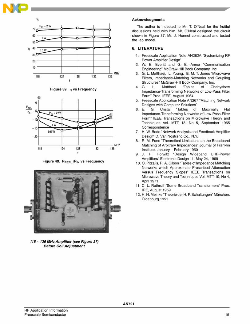
Figure 39. vs Frequency
-- 20
118 124 128 132 136MHz
0.5 W
1 W
Pin
db.
f
-- 15
-- 10
-- 5
0
PIN = 2 W
Prefl.
Figure 40. PREFL./PIN vs Frequency
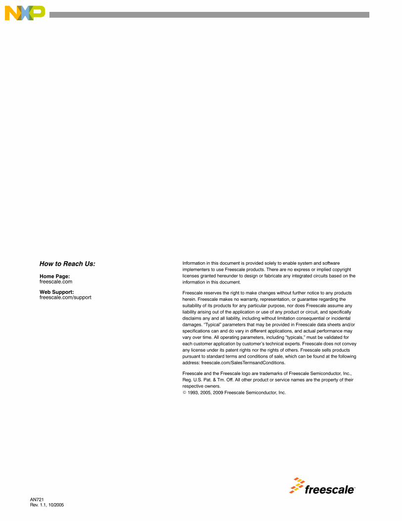
118 - 136 MHz Amplifier (see Figure 37)Before Coil Adjustment
Acknowledgments
The author is indebted to Mr. T. O’Neal for the fruitfuldiscussions held with him. Mr. O’Neal designed the circuitshown in Figure 37; Mr. J. Hennet constructed and testedthe lab model.
6. LITERATURE
1. Freescale Application Note AN282A “Systemizing RFPower Amplifier Design”
2. W. E. Everitt and G. E. Anner “CommunicationEngineering” McGraw-Hill Book Company, Inc.
3. G. L. Matthaei, L. Young, E. M. T. Jones “MicrowaveFilters, Impedance-Matching Networks and CouplingStructures” McGraw-Hill Book Company, Inc.
4. G. L. Matthaei “Tables of ChebyshewImpedance-Transforming Networks of Low-Pass FilterForm” Proc. IEEE, August 1964
5. Freescale Application Note AN267 “Matching NetworkDesigns with Computer Solutions”
6. E. G. Cristal “Tables of Maximally FlatImpedance-Transforming Networks of Low-Pass-FilterForm” IEEE Transactions on Microwave Theory andTechniques Vol. MTT 13, No 5, September 1965Correspondence
7. H. W. Bode “Network Analysis and Feedback AmplifierDesign” D. Van Nostrand Co., N.Y.
8. R. M. Fano “Theoretical Limitations on the BroadbandMatching of Arbitrary Impedances” Journal of FranklinInstitute, January -- February 1950
9. J. H. Horwitz “Design Wideband UHF-PowerAmplifiers” Electronic Design 11, May 24, 1969
10. O. Pitzalis, R. A. Gilson “Tables of ImpedanceMatchingNetworks which Approximate Prescribed AttenuationVersus Frequency Slopes” IEEE Transactions onMicrowave Theory and Techniques Vol. MTT-19, No 4,April 1971
11. C. L. Ruthroff “Some Broadband Transformers” Proc.IRE, August 1959
12. H. H. Meinke “Theorie der H. F. Schaltungen”München,Oldenburg 1951
16RF Application InformationFreescale Semiconductor
AN721
Information in this document is provided solely to enable system and softwareimplementers to use Freescale products. There are no express or implied copyrightlicenses granted hereunder to design or fabricate any integrated circuits based on theinformation in this document.
Freescale reserves the right to make changes without further notice to any productsherein. Freescale makes no warranty, representation, or guarantee regarding thesuitability of its products for any particular purpose, nor does Freescale assume anyliability arising out of the application or use of any product or circuit, and specificallydisclaims any and all liability, including without limitation consequential or incidentaldamages. “Typical” parameters that may be provided in Freescale data sheets and/orspecifications can and do vary in different applications, and actual performance mayvary over time. All operating parameters, including “typicals,” must be validated foreach customer application by customer’s technical experts. Freescale does not conveyany license under its patent rights nor the rights of others. Freescale sells productspursuant to standard terms and conditions of sale, which can be found at the followingaddress: freescale.com/SalesTermsandConditions.
Freescale and the Freescale logo are trademarks of Freescale Semiconductor, Inc.,Reg. U.S. Pat. & Tm. Off. All other product or service names are the property of theirrespective owners.E 1993, 2005, 2009 Freescale Semiconductor, Inc.
How to Reach Us:
Home Page:freescale.com
Web Support:freescale.com/support
AN721Rev. 1.1, 10/2005