Embed Size (px)
Citation preview

ECS Journal of Solid State Science and Technology, 5 (6) P361-P367 (2016) P361
Impact of Film Morphology on Chemical Mechanical Polishingof TungstenKun Xu,∗,z Shih-Haur Shen, Jason Fung, Hassan Iravani, Ingemar Carlsson, Tzu-Yu Liu,Bogdan Swedek, Shou-Sung Chang,∗ Wen-chiang Tu, Tomohiko Kitajima,Katrina Mikhaylich, Brian Brown, Sidney Huey, and Fritz Redeker
CMP Division, Applied Materials Inc., Sunnyvale, California 94085, USA
This study investigated the effects of tungsten (W) film morphology on the chemical mechanical polishing (CMP) of W. Chemicalvapor deposited (CVD) W films with two distinctively different grain sizes were used for comparison. During polishing, W filmthickness and optical reflectance, friction, and pad temperature were monitored in-situ. It was found that larger-grained W film tooklonger to pass the initial low removal rate stage. By correlating four different sensor signals, comparing friction dependency on filmmorphology, in slurry vs. DIW, it was concluded that W CMP comprises three main stages. First is the low rate initiation stage:grain is being partially planarized, reflectance increases, friction decreases. Second is the transition stage: rate is ramping, grainbecomes fully planarized, optical reflectance reaches maximum, and friction becomes minimal followed by a significant rise causedby formation of tungsten oxide passivation layer on the planarized W surface. Third is the high and constant rate stage: passivationand removal occur in a repetitive cycle, friction is high and stable, optical reflectance changes as polishing reaches different filmdepths. In all three stages, pad temperature increases continuously as friction-induced heat dissipates, with the rate of temperatureincrease following that of friction magnitude.© The Author(s) 2016. Published by ECS. This is an open access article distributed under the terms of the Creative CommonsAttribution Non-Commercial No Derivatives 4.0 License (CC BY-NC-ND, http://creativecommons.org/licenses/by-nc-nd/4.0/),which permits non-commercial reuse, distribution, and reproduction in any medium, provided the original work is not changed in anyway and is properly cited. For permission for commercial reuse, please email: [email protected]. [DOI: 10.1149/2.0371606jss]All rights reserved.
Manuscript submitted February 1, 2016; revised manuscript received April 20, 2016. Published April 29, 2016.
Metal CMP has enabled integrated circuit (IC) scaling as sum-marized in Table I. Depending on metal types and their differentreactivity, different deposition methods are used. For example, alu-minum (Al), a highly reactive metal, is deposited by high-temperaturephysical vapor deposition (PVD); whereas copper (Cu) as a noblemetal is deposited by electrochemical plating (ECP) on top of a PVDCu seed layer; W is deposited by CVD as its precursors and reac-tion by-product are in the gaseous phase. CVD cobalt is emerging asa replacement for Cu in back-end-of-line interconnects as it can fillmuch smaller line widths. Given their superior gap fill ability, CVDand atomic layer deposition (ALD) will become more common as ICscaling continues to 10 nm and beyond.
CVD W and W CMP are widely used in IC manufacturing. WCMP was first introduced in 1995 as contact metal and enabled 0.35μm technology yield and defect readiness.1 More recently, CVD Wand W CMP enabled FinFET replacement metal gate (RMG)2 whenPVD Al could no longer fill in the small gate in the 3D structure.In addition to contact metal and gate metal in logic devices, W iswidely used in memory, where 3D NAND involves many steps ofCVD W and W CMP. CVD W grain size and crystalline orientationare dependent on many parameters, including the sub-layer films,ALD W nucleation, and CVD W deposition precursors and depositiontemperature.3 For instance, CVD W is mostly dominated by alphaphase with (110) orientation >80% at 400◦C, with some portion ofbeta phase (114) if CVD W temperature is higher.4 Different types ofW applications have different sub-layers and deposition conditions.For CVD W used in contact, sub-layers include Ti and TiN. For CVDW used in replacement metal gate applications, sub-layers includework function and barrier metals. Therefore, CVD W in differentapplications could have different morphologies. Understanding theimpact of film morphology on W CMP is critical for optimizingprocess integration.
The W CMP mechanism was first investigated by Kaufman in19915 and widely accepted as the mechanism for metal CMP in gen-eral, including Cu CMP, Al CMP, etc. He identified two steps: 1) oxi-dation to form passivation film, 2) mechanical removal of the metal ox-ide. The two processes are repeated until the desired amount of metal
∗Electrochemical Society Member.zE-mail: [email protected]
is removed. In competing theories, Kneer suggests that transgranu-lar fracture assisted by inter-granular corrosion under high polishingdown force,6 while Steina et al. suggest that dissolution of tungstenoxides is the primary non-mechanical W removal mechanism.7 Fur-ther, variables such as oxidizer types,8 concentration of chemicals andabrasives in the slurry9 were studied, producing insights into the WCMP mechanism from the electrochemical perspective. Other areas ofresearch considered pad asperity10 and W grain morphologies.4 Forexample, different CVD W deposition methods results in differentcombination of W grain orientations with varied ratio of (110) and(114) phases, and average removal rate (Ave. RR)4 decreases withfaction area of (114) area fraction increases.4 It is noteworthy thatmost studies are based on Ave. RR obtained by measuring W filmthickness before and after polishing and dividing the difference bypolishing time. However, using Ave. RR presents drawbacks. It doesnot account for potential variation in the removal rate over the courseof the polish, and conclusions based upon Ave. RR can therefore beskewed.
Equipment companies developed metrologies to monitor polishingin-situ based on various physical properties of the CMP system. Forexample, eddy current sensors could be used to study film thicknesschanges in real time, based on metal film conductivity, or optical re-flectance differences between metal and dielectric surfaces could beused to study the time taken to clear metal and reach the dielectricinterface.11–13 Real-time in-situ metrologies made it possible for thefirst time to study the dynamic change in W CMP. In more recent stud-ies, such metrologies were used to study W CMP; it was observed that1) Ave. RR has a non-linear relationship with polishing time; 2) lowinitial polishing rate coincides with low initial polishing temperature;3) both temperature and removal rate increase with polishing time.It was therefore concluded that low temperature was the root causeof the low initial removal rate.14,15 In a separate study, we reportedusing eddy current and optical sensors to study real-time changesin thickness and W surface reflectance. The correlation betweenreal-time removal rate and W real-time optical reflectance stronglysuggested that the low initial polishing rate was caused by grainmorphology.16
In this study, two additional in-situ metrologies were used: fric-tion sensor and pad temperature sensor. By taking advantage of fourdifferent sensor systems, this study further unveiled the W CMP andrate initiation mechanism. Moreover, it revealed intricate relationships
) unless CC License in place (see abstract). ecsdl.org/site/terms_use address. Redistribution subject to ECS terms of use (see 144.217.70.220Downloaded on 2018-05-30 to IP

P362 ECS Journal of Solid State Science and Technology, 5 (6) P361-P367 (2016)
Table I. Metal types, deposition methods, and applications in IC.
Metallization W Al Cu Al W Co
Application Contact Via Interconnect Interconnect –replace Alusing dual damascene
Metal Gate Metal Gate Contact/interconnect
Deposition Method CVD PVD ECP PVD CVD CVD or PVDCMP On-set 1)&2) 1995 By etch 2001 2007 2012 EmergingNode 1)&2) 0.35 μm 0.13 μm 45 nm 22 nm FINFETEnabling 1)&2) Yield/defect red. RC scaling electro migration HKMG FINFET HKMG
between friction and temperature, and their interplay in metal CMP. Itdemonstrates that W CMP is a complex system with all aspects of thesystem influencing the polishing rate, including W film morphology.
To further understand the impact of morphology in metal CMP ingeneral, Al CMP was also included in this study as a direct contrastto W CMP. This is because PVD Al has smooth surface, which isdistinctively different from CVD W’s rough surface. This comparisonindicates the impact of morphology is a general phenomenon in metalCMP, and is not limited to W CMP. In another word, the understandingof W morphology effects is not limited to W, but is applicable to othertype of metal if surface roughness is significant enough.
Experimental
300 mm blanket CVD W films were deposited using the AppliedMaterials 300 mm Centura R© iSprint
TMTungsten ALD/CVD system
on 300 mm oxide wafers. TiN was deposited on top of oxide, followedby ALD W and bulk CVD W to a final thickness of 2000 to 2200 Å.Different ALD W precursors were used to generate CVD W filmswith distinctively different morphologies: SiH4 for small grain andB2H6 for large grain. 300 mm blanket PVD Al film was depositedto a final thickness of 4000 Å using the Applied Materials 300 mmEndura R© system. Polishing apparatus was 300 mm Applied MaterialsReflexion R© LK system. The Reflexion R© LK polisher was equippedwith four different in-situ metrologies to measure the following prop-erties: real-time metal thickness, optical reflectance, polishing frictionforce, and pad temperature. The real time metal film thickness mea-surement relied on an eddy current sensor with the sensor’s signal indirect correlation to metal film thickness. With the ability to measurereal time film thickness, instantaneous removal rate was observableand the dynamic polishing behavior could therefore be investigated.Optical reflectance measurement of the film was achieved using alaser sensor to detect laser intensity reflected from wafer surface,which could be used to study surface roughness of the metal film.Polishing friction force between the polishing pad and wafer wasmeasured by platen motor torque. Pad temperature measurement wasachieved using an infer-red temperature sensor.
Polishing slurries were Cabot Microelectronics W or Al slurrywith flow rate at 300 ml/min and polishing pressure at 2 psi withplaten and head rotation speed at 90 rpm and 80 rpm. Polishing wasstopped at different stages using various end point methods. For in-stance, using real time thickness sensor to end polishing at 250 Åremaining thickness, allowed full characterization of polishing’s dy-namic behavior. In another case, using the optical reflectance sensor toend polishing when metal film reflectivity reached maximum allowedone to inspect surface roughness when grain was planarized to a fullextent. After taken out of polisher, W film surface morphologies werestudied and compared using Applied Materials SEMVisionTM at fieldof view (FOV) of 1 μm. For Al surface studies, a FOV of 8 μm wasused. To study friction without slurry, polish experiments with a DIWflow rate 300 ml/min and polishing pressure at 2 psi for 60 s wereconducted using new CVD W films as well as W films that had passedthe initiation stage. W film thicknesses were measured before andafter the experiments using KLA-Tencor’s RS-100. The polishing padfor all experiments was Dow Chemical’s IC1010 with conditioningdisk from Kinik; each polishing used ex-situ conditioning with 9 lbdown force for 3 min to ensure consistent pad asperity for all tests.
All W film polishing were conducted using same polishing head, pad,disk, and at similar ring life, pad life and disk life. Furthermore, sameliquid dispense point was used at same flow rate of 300 ml/min forboth slurry and DIW. It was vital to keep these factors constant whilevarying only W film types, or slurry verse DIW for friction forcestudy.
Results and Discussion
CVD W film morphology.—Figure 1 shows the surfaces of twotypes of CVD W films deposited with different processes. It wasreported in the literature that CVD W has a polycrystalline struc-ture, BCC with mixed orientations of (110) and (114), depending ondeposition conditions.4 While the actual grain orientation was not in-vestigated further in this study, SEM review showed the morphologiesto be distinctively different. The grain size was estimated to be ∼ 800Å for the large-grain film and grain shape appeared to be more or lesstriangular, with the top of the grain a single point. For the small-grainfilm, many more grains appeared within the 1 μm FOV, with the topof the grain a line. For comparison, PVD Al, which was used in thefirst two generations of RMG, was deposited at higher temperatureand had FCC (111) orientation, with the top of the surface a plane andmuch larger grain size (Figure 2). In Al deposition, crystal orientationis also affected by the process sequence of the sub-layer metal.17
It should be noted that the experiments for this study were per-formed on blanket wafers. For device wafers, grain formation insidethe features would be restricted by the feature size and side-wall andbottom trench film stack. In a previous report on Al studies, it wasfound that different feature sizes would result in different ratios of Alto its wetting layer, therefore forming different types of Al alloy anddifferent resistivity.18 However, the polishing of bulk W in the field ofa device wafer would produce phenomena similar to those observedin this blanket wafer study, only more complex as the field wouldhave more sub-layers, including TiN and work-function metal in thecase of RMG. Each sub-layer could influence subsequent depositionsand the final CVD W grain. This paper focuses on the influence ofmorphology on CMP, rather than the cause of the morphology change.Nonetheless, it is important to note that processes upstream of CMPcould have a critical impact on CMP from an integration point of view.
Figure 1. SEM plan view of as-deposited CVD W films with different grainsize using 1 μm FOV.
) unless CC License in place (see abstract). ecsdl.org/site/terms_use address. Redistribution subject to ECS terms of use (see 144.217.70.220Downloaded on 2018-05-30 to IP

ECS Journal of Solid State Science and Technology, 5 (6) P361-P367 (2016) P363
Source: Applied Materials
Figure 2. SEM plan view of as-deposited PVD Al film using 8 μm FOV.
Figure 3. W removal rate evolutions for CVD W films using real-time eddycurrent sensor.
W CMP removal rate evolution: three distinctive rate stages char-acterized by four in-situ metrologies.—The two types of CVD Wfilms were polished and endpointed to thickness of 250 Å. As shownin Figure 3, real-time W film thickness was measured to reveal re-moval rate evolution throughout polishing. Based on this evolution,polishing could be divided into three stages (Table II), defined bytheir distinctive removal rates. In the first stage, removal rate wasvery low. In the 2nd stage, rate ramped up. At the 3rd stage, rate washigh and constant. It is apparent from Table II that the larger the Wgrain size, the longer it takes to transit the low-rate initiation stage.Although large-grain W film has a higher steady removal rate at stage3, its total Ave. RR appears to be lower due to its very long initia-
Table II. Summary of polishing stage duration and removal rate.
Stage 1 2 3 Total polish
Small-grain W film stage duration (sec.) 5 13 40 58Large-grain W film stage duration (sec.) 31 13 28 72
Stage 1 2 3 AverageSmall-grain W film removal rate (Å/min) 402 636 2520 1882Large-grain W film removal rate (Å/min) 90 1380 3480 1516
Figure 4. Calculated W CMP Ave. RR change by polishing time.
tion. By calculating the Ave. RR every 10 seconds and plotting thevalues against polishing time (Figure 4), a non-linear relationship be-tween Ave. RR and polishing time is observed. This is consistent withliterature reports that Ave. RR increases with polishing time.14,15
This result also indicates that using only Ave. RR to study the WCMP mechanism could be misleading. Ave. RR result is dependenton W film pre-thickness and total polishing time. For example, fromFigure 4, using 2000 Å CVD W film and 60 s of polishing time, onecould conclude that large-grain film has a lower Ave. RR. But, if bothtypes of CVD W films are thick enough and could be polished for alonger time, with enough post-thickness measurable to calculate Ave.RR, an opposite conclusion could be predicted. Assuming CVD Wfilm’s surface roughness does not change when thickness increases,such that stage 1, 2 times are same as shown in Table II, and only stage3 polishing time increases with thickness increase. Figure 5 plots pre-dicted Ave. RR against total polishing time: the predicted Ave. RRswitches over between the two types of film when total polishingtime is over 100 s. Instead of using Ave.RR, using real-time thicknessmeasurement reveals the true reason behind the apparent non-linearbehavior was removal rate evolution—three distinctive stages of pol-ishing, with the duration and removal rate of each being dependent onW morphology. This was further proved by using in-situ metrologies,including optical reflectance, friction, and pad temperature in additionto off-line SEM review.
Figure 5. Predicted W CMP Ave. RR change by total polishing time.
) unless CC License in place (see abstract). ecsdl.org/site/terms_use address. Redistribution subject to ECS terms of use (see 144.217.70.220Downloaded on 2018-05-30 to IP

P364 ECS Journal of Solid State Science and Technology, 5 (6) P361-P367 (2016)
Figure 6. Al CMP removal rate evolution for PVD Al film using real-timeeddy current sensor.
In comparison, PVD Al with a much smoother surface when pol-ished from 4000 Å to 250 Å, showed no low-rate initiation (Figure6). Removal rate was high immediately after polishing started. Thisis another proof that morphology has direct impact on rate initiationin metal CMP.
To understand the correlation of the four in-situ signals (W filmthickness, W film optical reflectance, friction, and pad temperature)and their revelation of rate initiation mechanism, they were plotted inFigure 7 and Figure 8 for small-grain CVD W film and large-grainCVD W film respectively. In both cases, as polishing progresses, op-tical reflectance increases as the W grain is planarized, peaks, thendecreases; initial friction is relatively high, then decreases to a mini-mum before increasing to a high plateau. Such friction evolution wasalso observed on a different polishing tool, indicating that this frictionchange was not unique to the polishing tool but rather was charac-teristic of the W CMP itself.15 For both films, instant removal rate,optical reflectance, and friction all synchronized to reveal polishingcharacteristics at different stages. The onset of stage 2 starts whenfriction force reaches minimum. Stage 3 commences when instantremoval rate reaches a high steady state, optical reflectance reachesmaximum, and friction reaches a high plateau. The pad temperatureon the other hand shows a cumulative effect from friction-generatedheat dissipation: for both films, pad temperature increases with pol-
Figure 7. Real-time thickness, optical reflectance, friction, and pad tempera-ture for small-grain W film during polish.
Figure 8. Real-time thickness, optical reflectance, friction, and pad tempera-ture for large-grain W film during polish.
ishing progress, measuring 30◦C higher when polishing ends at 250Å remaining.
W morphology impact on stage duration and characterizationof W morphologies at various stages.—To understand morphologyimpact each in-situ signal, each one of them was plotted for bothsmall-grain and large-grain W film as shown in Figure 3, Figure 9,Figure 10, and Figure 11. In each graph, stage 1 and stage 2 transitionswere marked using blue and red vertical lines respectively. Figure 9shows that as polishing starts, the small-grain W film is smoother thanthe large-grain W film with higher initial optical reflectance; it takesmuch less time to reach maximum reflectance, an indication of fullgrain planarization. After planarization, reflectance decreases slowlywhile the large-grain film is significantly more reflective. In Figure 10,both films have rough surfaces at the start of the polishing and haverelatively high friction. As polishing progresses, fiction decreases asthe grain is being planarized and reaches a minimum at end of stage1. What is most interesting is the subsequent significant increase infriction during stage 2. It is speculated that this abrupt rise results fromthe formation of a tungsten oxide (WOx) complex passivation layer,a much more brittle material than W. WOx promotes the onset of sig-nificant wear, resulting in higher friction. By correlating friction withoptical reflectance, it is concluded that enough W grain planarization
Figure 9. Optical reflectance for CVD W films using optical sensor.
) unless CC License in place (see abstract). ecsdl.org/site/terms_use address. Redistribution subject to ECS terms of use (see 144.217.70.220Downloaded on 2018-05-30 to IP

ECS Journal of Solid State Science and Technology, 5 (6) P361-P367 (2016) P365
Figure 10. Polishing friction for CVD W films using friction sensor.
is required to allow a large area of W to be in contact with the padand to form passivation across the wafer. When optical reflectance isstill low, as shown in Figure 9 before stage 2, surface is rough, frictioncontinues to go down. It is only at the onset of stage 2, when opticalreflectance climbs up to a certain degree that friction starts to hikeup rapidly. The subsequent abrasion of the passivation layer, in turn,jump starts the high and steady rate of stage 3. Figure 10 shows thatlarge-grain film takes much longer time to reach minimal friction, i.e.,it has an extended initiation stage. Once friction increases again, thelarge-grain film has higher friction and higher stage 3 removal rate thanthe small-grain film. It is possible the morphology difference couldhave resulted in different types of passivation layer that contributedto the friction and rate difference. Moreover, W film morphology viaits influence on friction, influences pad temperature (Figure 11). Forlarge-grain film, pad temperature shows a significant hike at stage 2,coinciding with a similar significant rise in friction. For small-grainfilm, stage 1 is short; the onset of stage 2 may not appear as obviousas in large-grain film. However, with careful observation, the changein temperature rise slope indeed reveals the transition between stage 1and stag 2. After onset of stage 2, a clear correlation between frictionand pad temperature is obvious: increase in pad temperature more or
Figure 11. Polishing pad temperature for CVD W films using infra-red tem-perature sensor.
less following the increase in friction. Toward the end of polishing,pad temperature stops rising coincident with a drop in friction. Thissuggests that pad temperature rise is strongly influenced by frictionfor both types of W films.
A set of W films was polished and stopped half way throughthe initiation stage, at the end of initiation (stage 2), and at 250 Åremaining. SEM review revealed initial grain morphology differencesand grain morphology evolution throughout the polishing process(Figure 12). Half way through initiation, both films show the topgrains partially planarized with large voids visible between them. Atend of stage 2, the top grains are fully planarized. The in-situ eddycurrent sensor indicates that grain planarization requires 163 Å Wremoval for small-grain film and 458 Å removal for large-grain film,resulting in a post-initiation remaining thickness of 1851 Å for theformer and 1726 Å for the latter. At 250 Å remaining, grain sizelooks smaller than at the end of stage 2, when both films are about1800 Å thick. This suggests grain size is not fixed but changes in thethickness direction. The morphology observation is consistent withoptical reflectance evolution after grain planarization that reveals thepolish reaching different cross-sections of the W grains with varied
Figure 12. SEM plan view of as-deposited CVD W films with different grain size at different stages using 1 μm FOV.
) unless CC License in place (see abstract). ecsdl.org/site/terms_use address. Redistribution subject to ECS terms of use (see 144.217.70.220Downloaded on 2018-05-30 to IP
P366 ECS Journal of Solid State Science and Technology, 5 (6) P361-P367 (2016)
Figure 13. Polishing friction and pad temperature for as-deposited CVD Wfilms during 60s of DIW polishing.
morphologies. It is possible that CVD W that is closer to ALD W isinfluenced to a greater degree by the ALD W than CVD W that isfarther away.
Friction of polishing CVD W films with different morphologiesand friction’s impact on pad temperature.—To further understandthe friction decrease during initiation and its quick rise after initia-tion, as-deposited W films were polished in DIW at the same flowrate, and friction and pad temperature were compared (Figure 13).As-deposited W films (both large- and small-grain) with rough sur-faces displayed high friction that decreased as polishing progressed.W film thickness measurements taken before and after DIW polishingshowed no W removal. It is understandable that a rougher surfacewill cause more digging into the pad surface that creates higher fric-tion than a smoother surface does. Although pure mechanical frictionresulted in removal of the top of the W grain, the volume was sosmall that the amount of removal was undetectable from Rs measure-ments. Small-grain W films showed more friction force reduction in60s of DIW polishing compared to the large-grain film, suggestingthat it would be easier to smooth out a rougher surface in the smaller-grain film. This observation was consistent with their initial frictionchange in slurry, where it quickly dropped to a minimum. Hence,grain planarization happens in both slurry and DIW, but the processis significantly slower in DIW due to the absence of abrasive parti-cles. It was also noted that temperature rises steadily in DIW polishing;large-grain W film with higher friction produces a greater temperatureincrease.
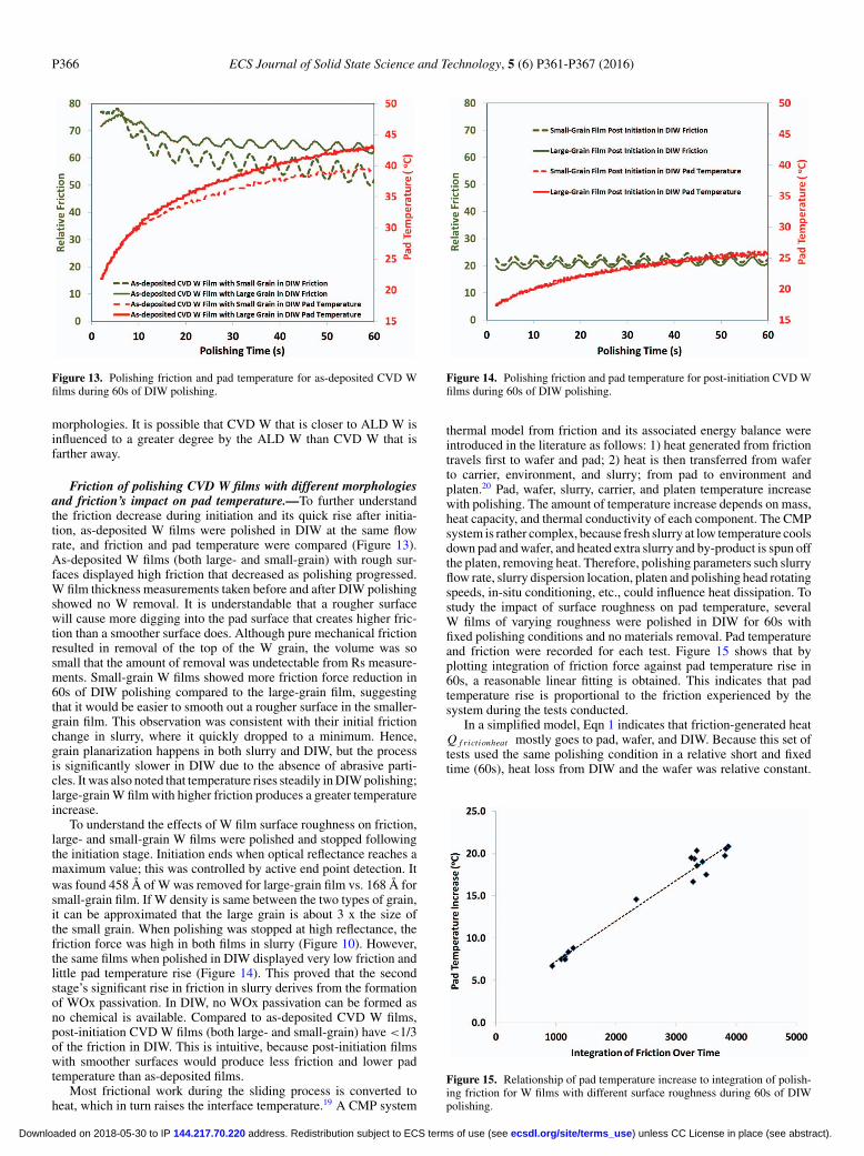
To understand the effects of W film surface roughness on friction,large- and small-grain W films were polished and stopped followingthe initiation stage. Initiation ends when optical reflectance reaches amaximum value; this was controlled by active end point detection. Itwas found 458 Å of W was removed for large-grain film vs. 168 Å forsmall-grain film. If W density is same between the two types of grain,it can be approximated that the large grain is about 3 x the size ofthe small grain. When polishing was stopped at high reflectance, thefriction force was high in both films in slurry (Figure 10). However,the same films when polished in DIW displayed very low friction andlittle pad temperature rise (Figure 14). This proved that the secondstage’s significant rise in friction in slurry derives from the formationof WOx passivation. In DIW, no WOx passivation can be formed asno chemical is available. Compared to as-deposited CVD W films,post-initiation CVD W films (both large- and small-grain) have <1/3of the friction in DIW. This is intuitive, because post-initiation filmswith smoother surfaces would produce less friction and lower padtemperature than as-deposited films.
Most frictional work during the sliding process is converted toheat, which in turn raises the interface temperature.19 A CMP system
Figure 14. Polishing friction and pad temperature for post-initiation CVD Wfilms during 60s of DIW polishing.
thermal model from friction and its associated energy balance wereintroduced in the literature as follows: 1) heat generated from frictiontravels first to wafer and pad; 2) heat is then transferred from waferto carrier, environment, and slurry; from pad to environment andplaten.20 Pad, wafer, slurry, carrier, and platen temperature increasewith polishing. The amount of temperature increase depends on mass,heat capacity, and thermal conductivity of each component. The CMPsystem is rather complex, because fresh slurry at low temperature coolsdown pad and wafer, and heated extra slurry and by-product is spun offthe platen, removing heat. Therefore, polishing parameters such slurryflow rate, slurry dispersion location, platen and polishing head rotatingspeeds, in-situ conditioning, etc., could influence heat dissipation. Tostudy the impact of surface roughness on pad temperature, severalW films of varying roughness were polished in DIW for 60s withfixed polishing conditions and no materials removal. Pad temperatureand friction were recorded for each test. Figure 15 shows that byplotting integration of friction force against pad temperature rise in60s, a reasonable linear fitting is obtained. This indicates that padtemperature rise is proportional to the friction experienced by thesystem during the tests conducted.
In a simplified model, Eqn 1 indicates that friction-generated heatQ f rictionheat mostly goes to pad, wafer, and DIW. Because this set oftests used the same polishing condition in a relative short and fixedtime (60s), heat loss from DIW and the wafer was relative constant.
Figure 15. Relationship of pad temperature increase to integration of polish-ing friction for W films with different surface roughness during 60s of DIWpolishing.
) unless CC License in place (see abstract). ecsdl.org/site/terms_use address. Redistribution subject to ECS terms of use (see 144.217.70.220Downloaded on 2018-05-30 to IP

ECS Journal of Solid State Science and Technology, 5 (6) P361-P367 (2016) P367
In Eqn 2, the increase in pad temperature is dependent on the heatabsorbed by the pad divided by pad’s heat capacity Cpad and its massMpad . Assuming heat loss from the wafer and DIW are constant, padtemperature increase is then proportional to friction-generated heat,which in turn is proportional to the friction work measured by the sys-tem. It is important to note that equilibrium is not reached within 60s.Given long enough polishing time, a much higher temperature fromthe system creates a larger temperature delta to its environment and,therefore, accelerates heat dissipation. Equilibrium could eventuallybe reached and temperature would reach steady state.19
Q f rictionheat = Q pad + Qwa f er + Q DI W [1]
�T pad = Q pad
Cpad ∗ Mpad= (
Q f rictionheat − Qwa f er − Q DI W
)/
(Cpad ∗ Mpad
) = a ∗ Q f rictionheat + b [2]
Variables contributing to CMP removal rate.—Friction and tem-perature play intricate roles in CMP. Friction is determined by manyfactors, including pad and film surface roughness, polishing down-force, friction coefficient, slurry and by-product flow rate, and theirlubrication effect. When there is no chemical reaction, only mechan-ical friction, temperature rises as a result of friction-generated heat.With slurry polishing involving chemical reaction, the situation willbe more complex as heat is used to overcome activation energy to ac-celerate the reaction and could be released in an exothermal reaction.Most metal oxidation reactions are exothermal. A rise in tempera-ture is a result of both friction and chemical reaction, but it could, inturn, impact friction and chemical reaction. Higher temperature couldaccelerate the chemical reaction, change pad modulus, and likely in-crease friction further. It was not the intention of this paper to addressall aspects of relevant variables in CMP, but to raise awareness of theimplications of film morphology as a factor often overlooked. Dif-ferent metals have different crystalline orientation. Same metal, butdifferent deposition methods further impact crystalline phases. Thecombined effects determine metal film surface roughness. Three ex-amples were illustrated in this study: PVD Al with FCC (110) smoothsurface, CVD W with SiH4 based ALD W precursor with rough sur-face but small grain size, CVD W with B2H6 based ALD W precursorwith rough surface but large grain size. Film’s morphology determinedmetal CMP’s rate initiation: the rougher the surface, the longer theinitiation. It is expected rate initiation could exist for other metal CMP,if metal film’s surface roughness is significant enough.
Conclusions
It is concluded that W morphology determines rate initiation andthat W CMP can be divided into three distinctive stages of polishing 1)grain partial planarization at a very low rate, 2) grain full planarizationand formation of large surface area of WOx passivation, and 3) highand constant removal rate with passivation and abrasion proceedingin repetitive cycles. Formation of WOx passivation in a large enoughsurface area, i.e., the chemical component of W CMP, is dependent onthe kinetics of the reaction: sufficient planarization of grain is requiredto allow enough of the W film surface to be in contact with slurry andpad. Further, grain morphology plays an important role in friction,which in turn affects removal rate and polishing temperature. Finally,metal morphology affects not only W CMP but extends to other metalfilms if the film roughness is significant enough.
References
1. J. M. Steigerwald, presented at the International Conference on Planarization/CMPTechnology, Fukuoka, Japan, Nov. 2009 (unpublished).
2. Intel press release for 20 nm trigate from Intel website.3. S. H. Kim, S. J. Yeom, N. Kwak, and H. Sohn, J. Electrochem. Soc., 155, 148 (2008).4. R. K. Maynard, S. J. Pearton, and R. K. Singh, J. Electrochem. Soc., 149, 648 (2002).5. F. B. Kaufman, D. B. Thompson, R. E. Broadie, M. A. Jaso, W. L. Guthrie,
D. J. Pearson, and M. B. Small, J. Electrochem. Soc. 138, 3460 (1991).6. E. A. Kneer, C. Raghunath, V. Mathew, S. Raghavan, and J. S. Jeon, J. Electrochem.
Soc., 144, 3041 (1997).7. D. J. Stein, D. L. Hetherington, and J. L. Cecchi, J. Materials Research, 14(9), 3695
(1999).8. Y.-J. Seo and W.-S. Lee, Materials Sci. and Eng. B 118, 281 (2005).9. Ed Paul, J. Electrochem. Soc., 148, 359 (2001).
10. S. B. Yeruva, C. W. Park, Y. I. Rabinovich, and B. M. Moudgil, J. Electrochem. Soc.156(10), 408 (2009).
11. B. W. Adams, B. Swedek, R. Bajaj, F. Redeker, M. Birang, and G. Amico, Semicon-ductor Fabtech, 12 (2000).
12. S. Huey, B. Chandrasekaran, D. Bennett, S. Tsai, K. Xu, J. Qian, S. Dhandapani,J. David, B. Swedek, and L. Karuppiah, ECS Trans. 44, 543 (2012).
13. K. Xu, Y. Chen, H. Iravani, Y. Wang, B. Swedek, M. Yu, Y. Wang, W. C. Tu, S. Xia,and L. Karuppiah, ECS Trans. 33, 69 (2010).
14. Z. Wang, R. Peng, S. Xia, T. Kitajima, and S. Tsai, ECS Trans. 41, 103 (2012).15. H. J. Kim, S. G. Ahn, L. Qin, D. Koli, V. Govingdarajulu, and Y. Moon, ECS J. Solid
State Sci. and Technology, 3, 310 (2014).16. K. Xu, T. Y. Liu, S. H. Shen, Y. Wang, I. Carlsson, B. Swedek, T. Kitajima, and
W. C. Tu, Paper 1422 presented at The Electrochemical Society Meeting, Orlando,FL, May, 2014.
17. H. Shibata, M. Murota, and K. Hashimoto, Jpn. J. Appl. Phys. 32, 4479 (1993).18. K. Xu, Y. Wang, S. H. Shen, X. Xia, W. Ch. Tu, L. Karuppiah, H. Yang, Z. Ge, Y. Lei,
M. Allen, N. Yoshida, L. W. Chang, B. Liu, M. Okazaki, and A. Brand, MRS onlineProceeding Library 1372 December (2011).
19. M. Amiri and M. M. Khonsari, Entropy 12, 1021 (2010).20. Z. Li, L. Borucki, I. Koshiyama, and A. Philipossian, J. Electochem. Soc., 157, 482
(2004).
) unless CC License in place (see abstract). ecsdl.org/site/terms_use address. Redistribution subject to ECS terms of use (see 144.217.70.220Downloaded on 2018-05-30 to IP