Embed Size (px)
Citation preview
www.intelligentmemory.com 1 IMM1G72D2RDD4AG
We Listen to Your Comments
Any information within this document that you feel is wrong, unclear or missing at all? Your feedback will help us to continuously improve the quality of this document. Please send your proposal (including a reference to this document) to: [email protected]
Datasheet | Rev. 1.0 | 2019
IMM1G72D2RDD4AG (Die Revision B) 8GByte (1024M x 72 Bit)
8GB DDR2 Registered DIMM RoHS Compliant Product
Remark:Remark:Remark:Remark: Please refer to the last page of the i) Contents ii) List of Table iii) List of Figures.
www.intelligentmemory.com 2 IMM1G72D2RDD4AG
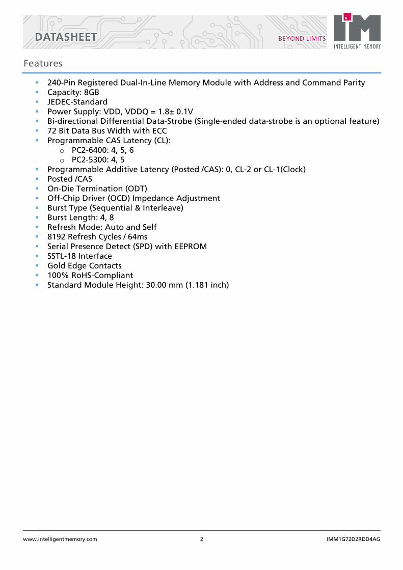
Features
240-Pin Registered Dual-In-Line Memory Module with Address and Command Parity Capacity: 8GB JEDEC-Standard Power Supply: VDD, VDDQ = 1.8± 0.1V Bi-directional Differential Data-Strobe (Single-ended data-strobe is an optional feature) 72 Bit Data Bus Width with ECC Programmable CAS Latency (CL):
o PC2-6400: 4, 5, 6 o PC2-5300: 4, 5
Programmable Additive Latency (Posted /CAS): 0, CL-2 or CL-1(Clock) Posted /CAS On-Die Termination (ODT) Off-Chip Driver (OCD) Impedance Adjustment Burst Type (Sequential & Interleave) Burst Length: 4, 8 Refresh Mode: Auto and Self 8192 Refresh Cycles / 64ms Serial Presence Detect (SPD) with EEPROM SSTL-18 Interface Gold Edge Contacts 100% RoHS-Compliant Standard Module Height: 30.00 mm (1.181 inch)
www.intelligentmemory.com 3 IMM1G72D2RDD4AG
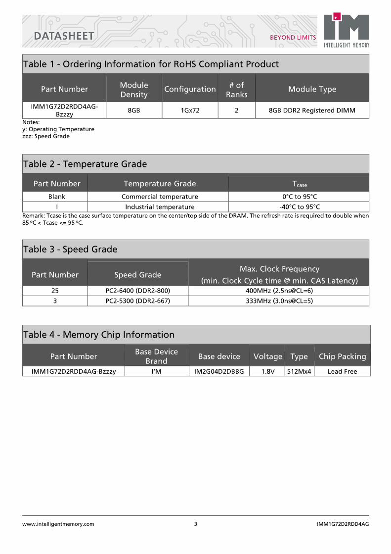
Table 1 - Ordering Information for RoHS Compliant Product
Part Number Module Density
Configuration # of Ranks
Module Type
IMM1G72D2RDD4AG-Bzzzy
8GB 1Gx72 2 8GB DDR2 Registered DIMM
Notes: y: Operating Temperature zzz: Speed Grade
Remark: Tcase is the case surface temperature on the center/top side of the DRAM. The refresh rate is required to double when 85 oC < Tcase <= 95 oC.
Table 3 - Speed Grade
Part Number Speed Grade Max. Clock Frequency
(min. Clock Cycle time @ min. CAS Latency) 25 PC2-6400 (DDR2-800) 400MHz (2.5ns@CL=6)
3 PC2-5300 (DDR2-667) 333MHz (3.0ns@CL=5)
Table 4 - Memory Chip Information
Part Number Base Device
Brand Base device Voltage Type Chip Packing
IMM1G72D2RDD4AG-Bzzzy I’M IM2G04D2DBBG 1.8V 512Mx4 Lead Free
Table 2 - Temperature Grade
Part Number Temperature Grade Tcase
Blank Commercial temperature 0°C to 95°C
I Industrial temperature -40°C to 95°C
www.intelligentmemory.com 4 IMM1G72D2RDD4AG
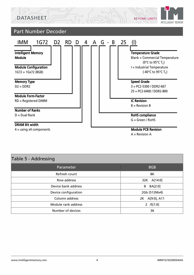
Part Number Decoder
IMM 1G72 D2 RD D 4 A G - B 25 (I)
Intelligent MemoryIntelligent MemoryIntelligent MemoryIntelligent Memory Temperature GradeTemperature GradeTemperature GradeTemperature Grade
ModuleModuleModuleModule Blank = Commercial Temperature
(0°C to 95°C TC)
Module ConfigurationModule ConfigurationModule ConfigurationModule Configuration I = Industrial Temperature
1G72 = 1Gx72 (8GB) (-40°C to 95°C TC)
Memory TypeMemory TypeMemory TypeMemory Type Speed GradeSpeed GradeSpeed GradeSpeed Grade
D2 = DDR2 3 = PC2-5300 / DDR2-667
25 = PC2-6400 / DDR2-800
Module Form-FactorModule Form-FactorModule Form-FactorModule Form-Factor
RD = Registered DIMM IC RevisionIC RevisionIC RevisionIC Revision
B = Revision B
Number of RanksNumber of RanksNumber of RanksNumber of Ranks
D = Dual Rank RoHS complianceRoHS complianceRoHS complianceRoHS compliance
G = Green / RoHS
DRAM Bit widthDRAM Bit widthDRAM Bit widthDRAM Bit width
4 = using x4 components Module PCB RevisionModule PCB RevisionModule PCB RevisionModule PCB Revision
A = Revision A
Table 5 - Addressing
Parameter 8GB
Refresh count 8K
Row address 32K A[14:0]
Device bank address 8 BA[2:0]
Device configuration 2Gb (512Mx4)
Column address 2K A[9:0], A11
Module rank address 2 /S[1:0]
Number of devices 36
www.intelligentmemory.com 5 IMM1G72D2RDD4AG
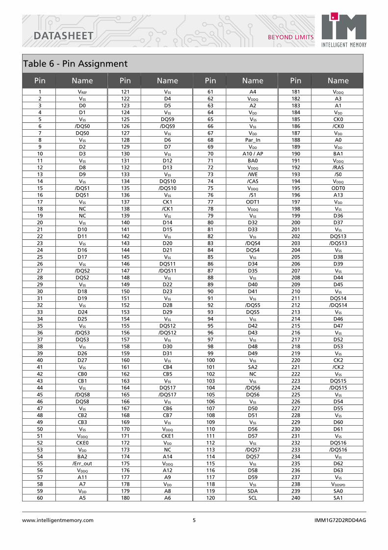
Table 6 - Pin Assignment
Pin Name Pin Name Pin Name Pin Name
1 VREF 121 VSS 61 A4 181 VDDQ
2 VSS 122 D4 62 VDDQ 182 A3
3 D0 123 D5 63 A2 183 A1
4 D1 124 VSS 64 VDD 184 VDD
5 VSS 125 DQS9 65 VSS 185 CK0
6 /DQS0 126 /DQS9 66 VSS 186 /CK0
7 DQS0 127 VSS 67 VDD 187 VDD
8 VSS 128 D6 68 Par_In 188 A0
9 D2 129 D7 69 VDD 189 VDD
10 D3 130 VSS 70 A10 / AP 190 BA1
11 VSS 131 D12 71 BA0 191 VDDQ
12 D8 132 D13 72 VDDQ 192 /RAS
13 D9 133 VSS 73 /WE 193 /S0
14 VSS 134 DQS10 74 /CAS 194 VDDQ
15 /DQS1 135 /DQS10 75 VDDQ 195 ODT0
16 DQS1 136 VSS 76 /S1 196 A13
17 VSS 137 CK1 77 ODT1 197 VDD
18 NC 138 /CK1 78 VDDQ 198 VSS
19 NC 139 VSS 79 VSS 199 D36
20 VSS 140 D14 80 D32 200 D37
21 D10 141 D15 81 D33 201 VSS
22 D11 142 VSS 82 VSS 202 DQS13
23 VSS 143 D20 83 /DQS4 203 /DQS13
24 D16 144 D21 84 DQS4 204 VSS
25 D17 145 VSS 85 VSS 205 D38
26 VSS 146 DQS11 86 D34 206 D39
27 /DQS2 147 /DQS11 87 D35 207 VSS
28 DQS2 148 VSS 88 VSS 208 D44
29 VSS 149 D22 89 D40 209 D45
30 D18 150 D23 90 D41 210 VSS
31 D19 151 VSS 91 VSS 211 DQS14
32 VSS 152 D28 92 /DQS5 212 /DQS14
33 D24 153 D29 93 DQS5 213 VSS
34 D25 154 VSS 94 VSS 214 D46
35 VSS 155 DQS12 95 D42 215 D47
36 /DQS3 156 /DQS12 96 D43 216 VSS
37 DQS3 157 VSS 97 VSS 217 D52
38 VSS 158 D30 98 D48 218 D53
39 D26 159 D31 99 D49 219 VSS
40 D27 160 VSS 100 VSS 220 CK2
41 VSS 161 CB4 101 SA2 221 /CK2
42 CB0 162 CB5 102 NC 222 VSS
43 CB1 163 VSS 103 VSS 223 DQS15
44 VSS 164 DQS17 104 /DQS6 224 /DQS15
45 /DQS8 165 /DQS17 105 DQS6 225 VSS
46 DQS8 166 VSS 106 VSS 226 D54
47 VSS 167 CB6 107 D50 227 D55
48 CB2 168 CB7 108 D51 228 VSS
49 CB3 169 VSS 109 VSS 229 D60
50 VSS 170 VDDQ 110 D56 230 D61
51 VDDQ 171 CKE1 111 D57 231 VSS
52 CKE0 172 VDD 112 VSS 232 DQS16
53 VDD 173 NC 113 /DQS7 233 /DQS16
54 BA2 174 A14 114 DQS7 234 VSS
55 /Err_out 175 VDDQ 115 VSS 235 D62
56 VDDQ 176 A12 116 D58 236 D63
57 A11 177 A9 117 D59 237 VSS
58 A7 178 VDD 118 VSS 238 VDDSPD
59 VDD 179 A8 119 SDA 239 SA0
60 A5 180 A6 120 SCL 240 SA1
www.intelligentmemory.com 6 IMM1G72D2RDD4AG
Table 7 - Pin Description
Pin Name Description Pin Name Description
VDD SDRAM core power supply VREF SDRAM I/O reference supply
A0-A14 SDRAM address bus VSS Power supply return (ground)
CK0-CK1 SDRAM clocks
(positive line of differential pair) BA0-BA2 SDRAM bank addresses
/RAS SDRAM row address strobe /CK0-/CK1 SDRAM clocks
(negative line of differential pair)
/WE SDRAM write enable /CAS SDRAM column address strobe
/S0-/S1 DIMM Rank Select Lines CKE0-CKE1 SDRAM clock enable lines
/RESET Reset Pin ODT0-ODT1 On-die termination control lines
DQS0-DQS17 SDRAM data strobes
(positive line of differential pair) /DQS0-/DQS17
SDRAM data strobes (negative line of differential pair)
D0-D63 DIMM memory data bus CB0-CB7 Data check bits Input/Output
/Err_Out Parity error found in the Address and
Control bus SDA EEPROM date line
Par_In Parity bit for the Address and Control bus SCL EEPROM clock
NC Spare Pins (no connect) SA0-SA1 EEPROM address input
VDDSPD EEPROM positive power supply - -
www.intelligentmemory.com 7 IMM1G72D2RDD4AG
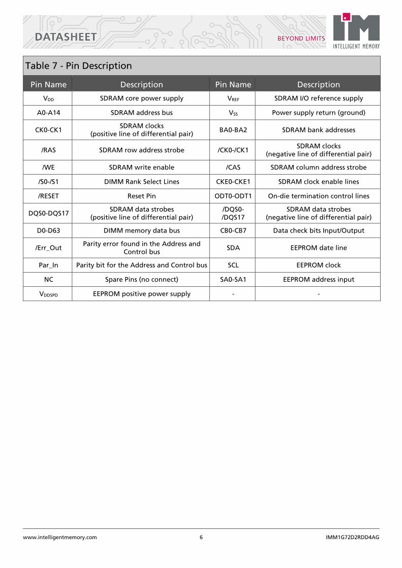
Module Dimension
Figure 1 – 240 Pin DDR2 SDRAM Registered DIMM
Table 8 - PCB Dimension
Symbol MIN NOM MAX
A 29.85 30.00 30.15
A1 10.00 Basic
A2 0.05 0.20 0.35
A3 17.80 Basic
D 133.20 133.35 133.50
D1 4.00 Basic
D2 2.50 Basic
e1 63.00 Basic
e2 55.00 Basic
E 4.00
Notes:
All dimensioning and tolerancing conform to ASME Y14.5M-1994. Tolerances for all dimensions ±0.15 unless otherwise specified. All dimensions are in millimeters.
A B
A
B
www.intelligentmemory.com 8 IMM1G72D2RDD4AG
Figure 2 – Functional Block Diagram (Page 1 of 3)
/S0
/S1
CKE0
CKE1
DQS
DM
CK
E
/CS
/DQS
D0-D3U9
DQS
DM
CK
E
/CS
/DQS
D0-D3U27
CB0-CB3
VSS
/DQS8
DQS8 DQS
DM
CK
E
/CS
/DQS
D0-D3U4
CB4-CB7
VSS
/DQS17
DQS17 DQS
DM
CK
E
/CS
/DQS
D0-D3U22
DQS
DM
CK
E
/CS
/DQS
D0-D3U8
DQS
DM
CK
E
/CS
/DQS
D0-D3U26
D24-D27
VSS
/DQS3
DQS3 DQS
DM
CK
E
/CS
/DQS
D0-D3U3
D28-D31
VSS
/DQS12
DQS12 DQS
DM
CK
E
/CS
/DQS
D0-D3U21
DQS
DM
CK
E
/CS
/DQS
D0-D3U7
DQS
DM
CK
E
/CS
/DQS
D0-D3U25
D16-D19
VSS
/DQS2
DQS2 DQS
DM
CK
E
/CS
/DQS
D0-D3U2
D20-D23
VSS
/DQS11
DQS11 DQS
DM
CK
E
/CS
/DQS
D0-D3U20
DQS
DM
CK
E
/CS
/DQS
D0-D3U6
DQS
DM
CK
E
/CS
/DQS
D0-D3U24
D8-D11
VSS
/DQS1
DQS1 DQS
DM
CK
E
/CS
/DQS
D0-D3U1
D12-D15
VSS
/DQS10
DQS10 DQS
DM
CK
E
/CS
/DQS
D0-D3U19
DQS
DMC
KE
/CS
/DQS
D0-D3U5
DQS
DM
CK
E
/CS
/DQS
D0-D3U23
D0-D3
VSS
/DQS0
DQS0 DQS
DM
CK
E
/CS
/DQS
D0-D3U0
D4-D7
VSS
/DQS9
DQS9 DQS
DM
CK
E
/CS
/DQS
D0-D3U18
www.intelligentmemory.com 9 IMM1G72D2RDD4AG
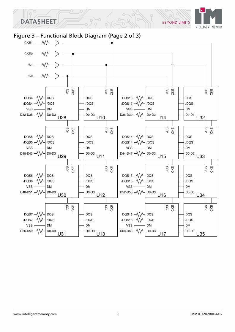
Figure 3 – Functional Block Diagram (Page 2 of 3)
/S0
/S1
CKE0
CKE1
DQS
DM
CK
E
/CS
/DQS
D0-D3U13
DQS
DM
CK
E
/CS
/DQS
D0-D3U31
D56-D59
VSS
/DQS7
DQS7 DQS
DM
CK
E
/CS
/DQS
D0-D3U17
D60-D63
VSS
/DQS16
DQS16 DQS
DM
CK
E
/CS
/DQS
D0-D3U35
DQS
DM
CK
E
/CS
/DQS
D0-D3U12
DQS
DM
CK
E
/CS
/DQS
D0-D3U30
D48-D51
VSS
/DQS6
DQS6 DQS
DM
CK
E
/CS
/DQS
D0-D3U16
D52-D55
VSS
/DQS15
DQS15 DQS
DM
CK
E
/CS
/DQS
D0-D3U34
DQS
DM
CK
E
/CS
/DQS
D0-D3U11
DQS
DM
CK
E
/CS
/DQS
D0-D3U29
D40-D43
VSS
/DQS5
DQS5 DQS
DM
CK
E
/CS
/DQS
D0-D3U15
D44-D47
VSS
/DQS14
DQS14 DQS
DM
CK
E
/CS
/DQS
D0-D3U33
DQS
DMC
KE
/CS
/DQS
D0-D3U10
DQS
DM
CK
E
/CS
/DQS
D0-D3U28
D32-D35
VSS
/DQS4
DQS4 DQS
DM
CK
E
/CS
/DQS
D0-D3U14
D36-D39
VSS
/DQS13
DQS13 DQS
DM
CK
E
/CS
/DQS
D0-D3U32
www.intelligentmemory.com 10 IMM1G72D2RDD4AG
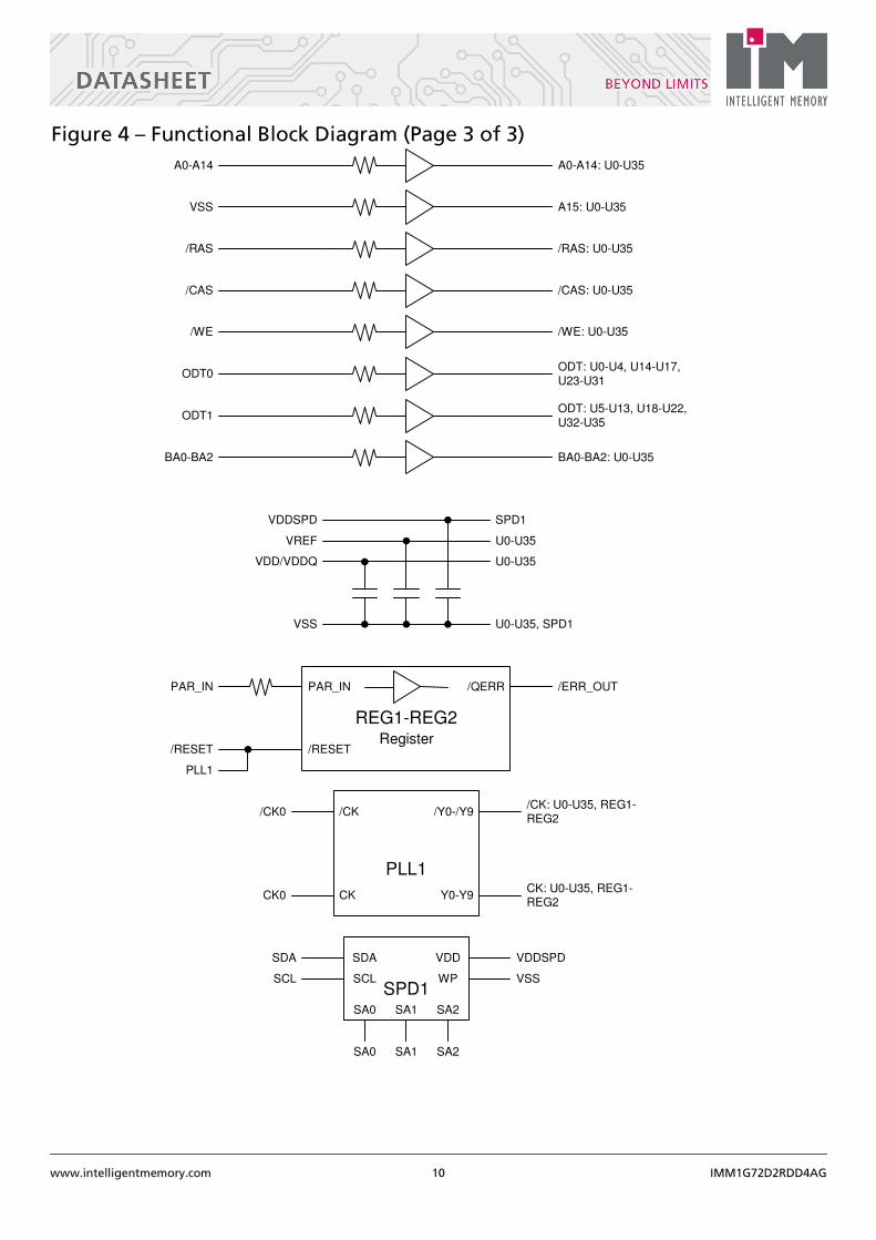
Figure 4 – Functional Block Diagram (Page 3 of 3)
A0-A14 A0-A14: U0-U35
/RAS
/CAS
/RAS: U0-U35
/CAS: U0-U35
VREF
VDD/VDDQ
VSS
U0-U35
U0-U35
U0-U35, SPD1
/CK
CK Y0-Y9
/Y0-/Y9
PLL1
/CK0
CK0
/CK: U0-U35, REG1-REG2
CK: U0-U35, REG1-REG2
VSS A15: U0-U35
/WE /WE: U0-U35
REG1-REG2
PAR_IN
BA0-BA2 BA0-BA2: U0-U35
/RESET/RESET
PLL1
ODT0ODT: U0-U4, U14-U17,U23-U31
Register
ODT1ODT: U5-U13, U18-U22,U32-U35
SCL
SDA
SA0 SA1 SA2
WP
VDD
SPD1
VDDSPD SPD1
PAR_IN
SDA
SCL
VDDSPD
VSS
SA0 SA1 SA2
/ERR_OUT/QERR
www.intelligentmemory.com 11 IMM1G72D2RDD4AG
Electrical Parameter
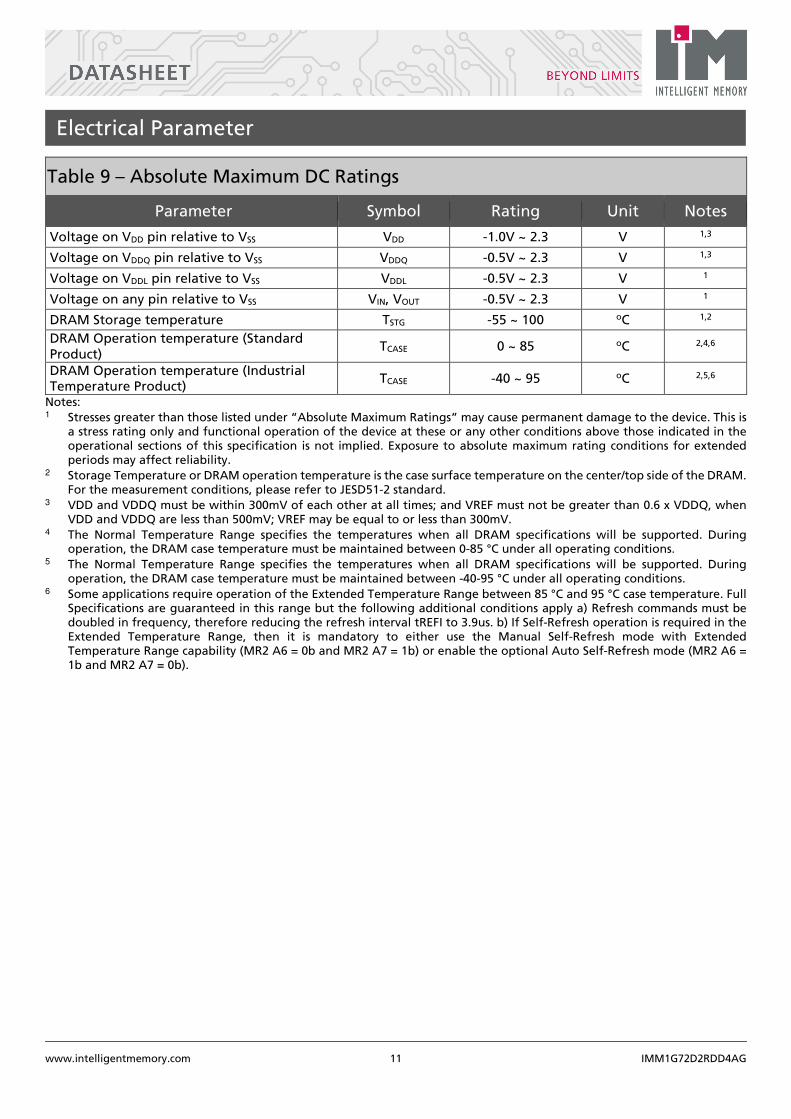
Table 9 – Absolute Maximum DC Ratings
Parameter Symbol Rating Unit Notes
Voltage on VDD pin relative to VSS VDD -1.0V ~ 2.3 V 1,3
Voltage on VDDQ pin relative to VSS VDDQ -0.5V ~ 2.3 V 1,3
Voltage on VDDL pin relative to VSS VDDL -0.5V ~ 2.3 V 1
Voltage on any pin relative to VSS VIN, VOUT -0.5V ~ 2.3 V 1
DRAM Storage temperature TSTG -55 ~ 100 oC 1,2
DRAM Operation temperature (Standard Product)
TCASE 0 ~ 85 oC 2,4,6
DRAM Operation temperature (Industrial Temperature Product)
TCASE -40 ~ 95 oC 2,5,6
Notes: 1 Stresses greater than those listed under “Absolute Maximum Ratings” may cause permanent damage to the device. This is
a stress rating only and functional operation of the device at these or any other conditions above those indicated in the operational sections of this specification is not implied. Exposure to absolute maximum rating conditions for extended periods may affect reliability.
2 Storage Temperature or DRAM operation temperature is the case surface temperature on the center/top side of the DRAM. For the measurement conditions, please refer to JESD51-2 standard.
3 VDD and VDDQ must be within 300mV of each other at all times; and VREF must not be greater than 0.6 x VDDQ, when VDD and VDDQ are less than 500mV; VREF may be equal to or less than 300mV.
4 The Normal Temperature Range specifies the temperatures when all DRAM specifications will be supported. During operation, the DRAM case temperature must be maintained between 0-85 °C under all operating conditions.
5 The Normal Temperature Range specifies the temperatures when all DRAM specifications will be supported. During operation, the DRAM case temperature must be maintained between -40-95 °C under all operating conditions.
6 Some applications require operation of the Extended Temperature Range between 85 °C and 95 °C case temperature. Full Specifications are guaranteed in this range but the following additional conditions apply a) Refresh commands must be doubled in frequency, therefore reducing the refresh interval tREFI to 3.9us. b) If Self-Refresh operation is required in the Extended Temperature Range, then it is mandatory to either use the Manual Self-Refresh mode with Extended Temperature Range capability (MR2 A6 = 0b and MR2 A7 = 1b) or enable the optional Auto Self-Refresh mode (MR2 A6 = 1b and MR2 A7 = 0b).
www.intelligentmemory.com 12 IMM1G72D2RDD4AG
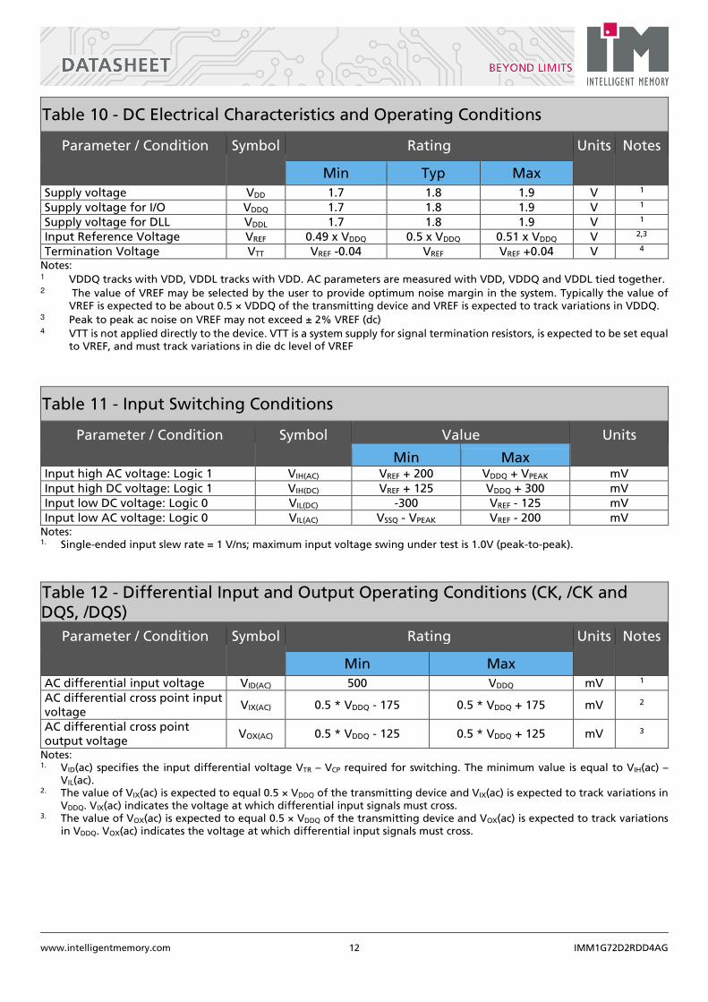
Table 10 - DC Electrical Characteristics and Operating Conditions
Parameter / Condition Symbol Rating Units Notes
Min Typ Max
Supply voltage VDD 1.7 1.8 1.9 V 1
Supply voltage for I/O VDDQ 1.7 1.8 1.9 V 1
Supply voltage for DLL VDDL 1.7 1.8 1.9 V 1
Input Reference Voltage VREF 0.49 x VDDQ 0.5 x VDDQ 0.51 x VDDQ V 2,3
Termination Voltage VTT VREF -0.04 VREF VREF +0.04 V 4
Notes: 1 VDDQ tracks with VDD, VDDL tracks with VDD. AC parameters are measured with VDD, VDDQ and VDDL tied together. 2 The value of VREF may be selected by the user to provide optimum noise margin in the system. Typically the value of
VREF is expected to be about 0.5 × VDDQ of the transmitting device and VREF is expected to track variations in VDDQ. 3 Peak to peak ac noise on VREF may not exceed ± 2% VREF (dc) 4 VTT is not applied directly to the device. VTT is a system supply for signal termination resistors, is expected to be set equal
to VREF, and must track variations in die dc level of VREF
Table 11 - Input Switching Conditions
Parameter / Condition Symbol Value Units
Min Max Input high AC voltage: Logic 1 VIH(AC) VREF + 200 VDDQ + VPEAK mV Input high DC voltage: Logic 1 VIH(DC) VREF + 125 VDDQ + 300 mV Input low DC voltage: Logic 0 VIL(DC) -300 VREF - 125 mV Input low AC voltage: Logic 0 VIL(AC) VSSQ - VPEAK VREF - 200 mV
Notes: 1. Single-ended input slew rate = 1 V/ns; maximum input voltage swing under test is 1.0V (peak-to-peak).
Table 12 - Differential Input and Output Operating Conditions (CK, /CK and DQS, /DQS)
Parameter / Condition Symbol Rating Units Notes
Min Max
AC differential input voltage VID(AC) 500 VDDQ mV 1
AC differential cross point input voltage
VIX(AC) 0.5 * VDDQ - 175 0.5 * VDDQ + 175 mV 2
AC differential cross point output voltage
VOX(AC) 0.5 * VDDQ - 125 0.5 * VDDQ + 125 mV 3
Notes: 1. VID(ac) specifies the input differential voltage VTR – VCP required for switching. The minimum value is equal to VIH(ac) –
VIL(ac). 2. The value of VIX(ac) is expected to equal 0.5 × VDDQ of the transmitting device and VIX(ac) is expected to track variations in
VDDQ. VIX(ac) indicates the voltage at which differential input signals must cross. 3. The value of VOX(ac) is expected to equal 0.5 × VDDQ of the transmitting device and VOX(ac) is expected to track variations
in VDDQ. VOX(ac) indicates the voltage at which differential input signals must cross.
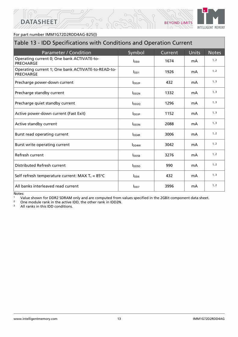
www.intelligentmemory.com 13 IMM1G72D2RDD4AG
For part number IMM1G72D2RDD4AG-B25(I)
Table 13 - IDD Specifications with Conditions and Operation Current
Parameter / Condition Symbol Current Units Notes Operating current 0; One bank ACTIVATE-to-PRECHARGE
IDD0 1674 mA 1, 2
Operating current 1; One bank ACTIVATE-to-READ-to-PRECHARGE
IDD1 1926 mA 1, 2
Precharge power-down current IDD2P 432 mA 1, 3
Precharge standby current IDD2N 1332 mA 1, 3
Precharge quiet standby current IDD2Q 1296 mA 1, 3
Active power-down current (Fast Exit) IDD3P 1152 mA 1, 3
Active standby current IDD3N 2088 mA 1, 3
Burst read operating current IDD4R 3006 mA 1, 2
Burst write operating current IDD4W 3042 mA 1, 2
Refresh current IDD5B 3276 mA 1, 2
Distributed Refresh current IDD5D 990 mA 1, 2
Self refresh temperature current: MAX Tc = 85oC IDD6 432 mA 1, 3
All banks interleaved read current IDD7 3996 mA 1, 2
Notes: 1 Value shown for DDR2 SDRAM only and are computed from values specified in the 2GBit component data sheet. 2 One module rank in the active IDD, the other rank in IDD2N. 3 All ranks in this IDD conditions.
www.intelligentmemory.com 14 IMM1G72D2RDD4AG
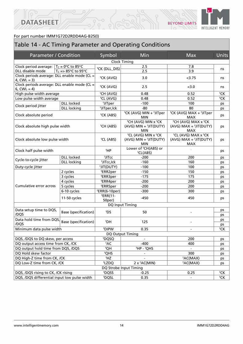
For part number IMM1G72D2RDD4AG-B25(I)
Table 14 - AC Timing Parameter and Operating Conditions
Parameter / Condition Symbol Min Max Units Clock Timing
Clock period average: DLL disable mode
TC = 0oC to 85oC tCK (DLL_DIS) 2.5 7.8
ns TC => 85oC to 95oC 2.5 3.9
Clock periods average: DLL enable mode (CL = 4, CWL = 3)
tCK (AVG) 3.0 <3.75 ns
Clock periods average: DLL enable mode (CL = 6, CWL = 4)
tCK (AVG) 2.5 <3.0 ns
High pulse width average tCH (AVG) 0.48 0.52 tCK
Low pulse width average tCL (AVG) 0.48 0.52 tCK
Clock period jitter DLL locked tJITper -100 100 ps
DLL locking tJITper,Ick -80 80 ps
Clock absolute period tCK (ABS) tCK (AVG) MIN + tJITper
MIN
tCK (AVG) MAX + tJITper MAX
ps
Clock absolute high pulse width tCH (ABS)
tCH (AVG) MIN x tCK (AVG) MIN + tJIT(DUTY)
MIN
tCH (AVG) MAX x tCK (AVG) MAX + tJIT(DUTY)
MAX ps
Clock absolute low pulse width tCL (ABS)
tCL (AVG) MIN x tCK (AVG) MIN + tJIT(DUTY)
MIN
tCL (AVG) MAX x tCK (AVG) MAX + tJIT(DUTY)
MAX ps
Clock half pulse width tHP Lower of tCH(ABS) or
tCL(ABS) - ps
Cycle-to-cycle jitter DLL locked tJITcc -200 200 ps
DLL locking tJITcc,Ick -160 160 ps
Duty-cycle jitter tJIT(DUTY) -100 100 ps
Cumulative error across
2 cycles tERR2per -150 150 ps
3 cycles tERR3per -175 175 ps
4 cycles tERR4per -200 200 ps
5 cycles tERR5per -200 200 ps
6-10 cycles tERR(6-10per) -300 300 ps
11-50 cycles tERR(11-50per)
-450 450 ps
DQ Input Timing
Data setup time to DQS, /DQS
Base (specification) tDS 50 - ps
ps
Data hold time from DQS, /DQS
Base (specification) tDH 125 - ps
ps
Minimum data pulse width tDIPW 0.35 - tCK
DQ Output Timing
DQS, /DQS to DQ skew, per access tDQSQ - 200 ps
DQ output access time from CK, /CK tAC -400 400 ps
DQ output hold time from DQS, /DQS tQH tHP - tQHS - ps
DQ Hold skew factor tQHS - 300 ps
DQ High-Z time from CK, /CK tHZ - tAC(MAX) ps
DQ Low-Z time from CK, /CK tLZDQ 2 x tAC(MIN) tAC(MAX) ps
DQ Strobe Input Timing
DQS, /DQS rising to CK, /CK rising tDQSS -0.25 0.25 tCK
DQS, /DQS differential input low pulse width tDQSL 0.35 - tCK
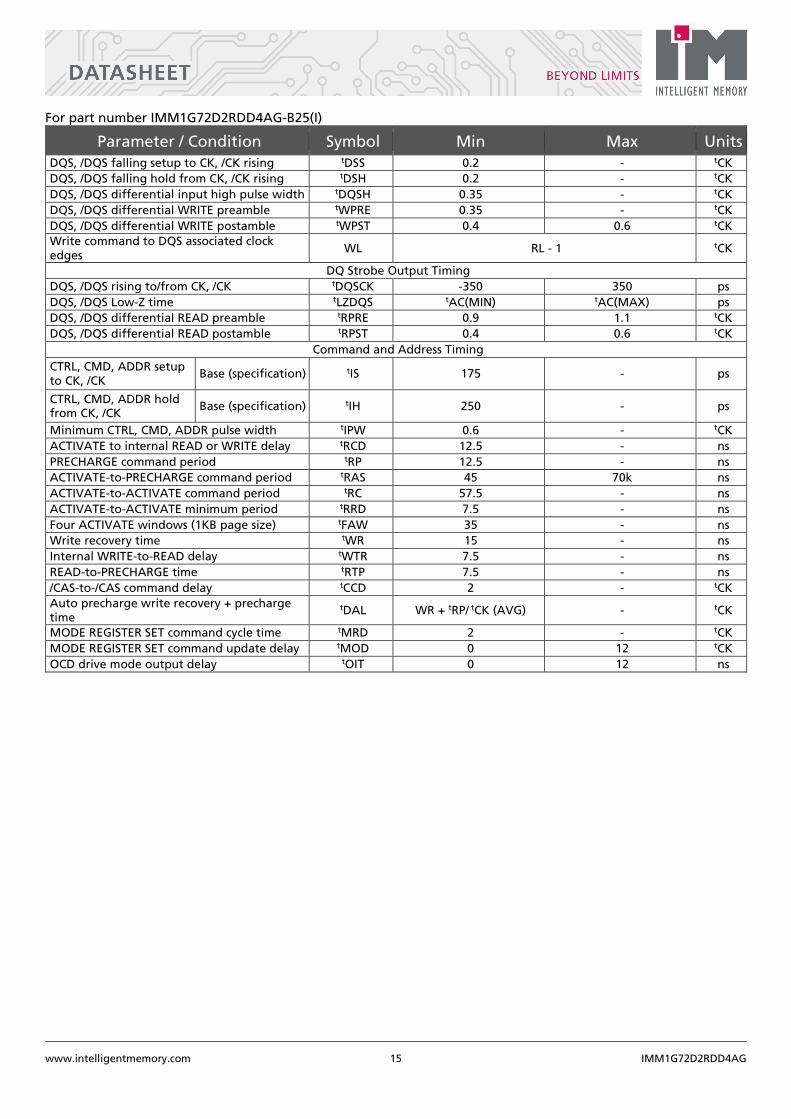
www.intelligentmemory.com 15 IMM1G72D2RDD4AG
For part number IMM1G72D2RDD4AG-B25(I)
Parameter / Condition Symbol Min Max Units DQS, /DQS falling setup to CK, /CK rising tDSS 0.2 - tCK
DQS, /DQS falling hold from CK, /CK rising tDSH 0.2 - tCK
DQS, /DQS differential input high pulse width tDQSH 0.35 - tCK
DQS, /DQS differential WRITE preamble tWPRE 0.35 - tCK
DQS, /DQS differential WRITE postamble tWPST 0.4 0.6 tCK
Write command to DQS associated clock edges
WL RL - 1 tCK
DQ Strobe Output Timing
DQS, /DQS rising to/from CK, /CK tDQSCK -350 350 ps
DQS, /DQS Low-Z time tLZDQS tAC(MIN) tAC(MAX) ps
DQS, /DQS differential READ preamble tRPRE 0.9 1.1 tCK
DQS, /DQS differential READ postamble tRPST 0.4 0.6 tCK
Command and Address Timing
CTRL, CMD, ADDR setup to CK, /CK
Base (specification) tIS 175 - ps
CTRL, CMD, ADDR hold from CK, /CK
Base (specification) tIH 250 - ps
Minimum CTRL, CMD, ADDR pulse width tIPW 0.6 - tCK
ACTIVATE to internal READ or WRITE delay tRCD 12.5 - ns
PRECHARGE command period tRP 12.5 - ns
ACTIVATE-to-PRECHARGE command period tRAS 45 70k ns
ACTIVATE-to-ACTIVATE command period tRC 57.5 - ns
ACTIVATE-to-ACTIVATE minimum period tRRD 7.5 - ns
Four ACTIVATE windows (1KB page size) tFAW 35 - ns
Write recovery time tWR 15 - ns
Internal WRITE-to-READ delay tWTR 7.5 - ns
READ-to-PRECHARGE time tRTP 7.5 - ns
/CAS-to-/CAS command delay tCCD 2 - tCK
Auto precharge write recovery + precharge time
tDAL WR + tRP/ tCK (AVG) - tCK
MODE REGISTER SET command cycle time tMRD 2 - tCK
MODE REGISTER SET command update delay tMOD 0 12 tCK
OCD drive mode output delay tOIT 0 12 ns
www.intelligentmemory.com 16 IMM1G72D2RDD4AG
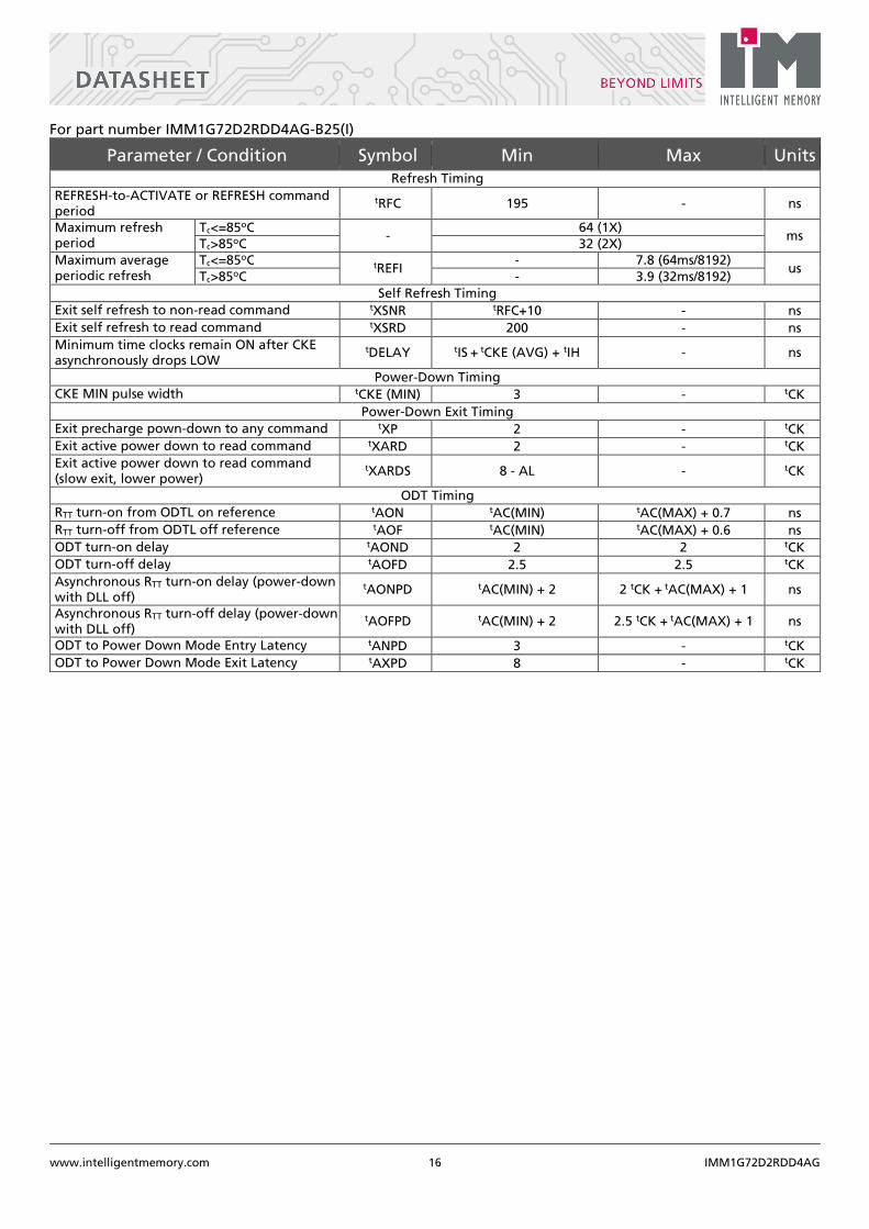
For part number IMM1G72D2RDD4AG-B25(I)
Parameter / Condition Symbol Min Max Units Refresh Timing
REFRESH-to-ACTIVATE or REFRESH command period
tRFC 195 - ns
Maximum refresh period
Tc<=85oC - 64 (1X)
ms Tc>85oC 32 (2X)
Maximum average periodic refresh
Tc<=85oC tREFI - 7.8 (64ms/8192)
us Tc>85oC - 3.9 (32ms/8192)
Self Refresh Timing
Exit self refresh to non-read command tXSNR tRFC+10 - ns
Exit self refresh to read command tXSRD 200 - ns
Minimum time clocks remain ON after CKE asynchronously drops LOW
tDELAY tIS + tCKE (AVG) + tIH - ns
Power-Down Timing
CKE MIN pulse width tCKE (MIN) 3 - tCK
Power-Down Exit Timing
Exit precharge pown-down to any command tXP 2 - tCK
Exit active power down to read command tXARD 2 - tCK
Exit active power down to read command (slow exit, lower power)
tXARDS 8 - AL - tCK
ODT Timing
RTT turn-on from ODTL on reference tAON tAC(MIN) tAC(MAX) + 0.7 ns
RTT turn-off from ODTL off reference tAOF tAC(MIN) tAC(MAX) + 0.6 ns
ODT turn-on delay tAOND 2 2 tCK
ODT turn-off delay tAOFD 2.5 2.5 tCK
Asynchronous RTT turn-on delay (power-down with DLL off)
tAONPD tAC(MIN) + 2 2 tCK + tAC(MAX) + 1 ns
Asynchronous RTT turn-off delay (power-down with DLL off)
tAOFPD tAC(MIN) + 2 2.5 tCK + tAC(MAX) + 1 ns
ODT to Power Down Mode Entry Latency tANPD 3 - tCK
ODT to Power Down Mode Exit Latency tAXPD 8 - tCK
www.intelligentmemory.com 17 IMM1G72D2RDD4AG
For part number IMM1G72D2RDD4AG-B25(I)
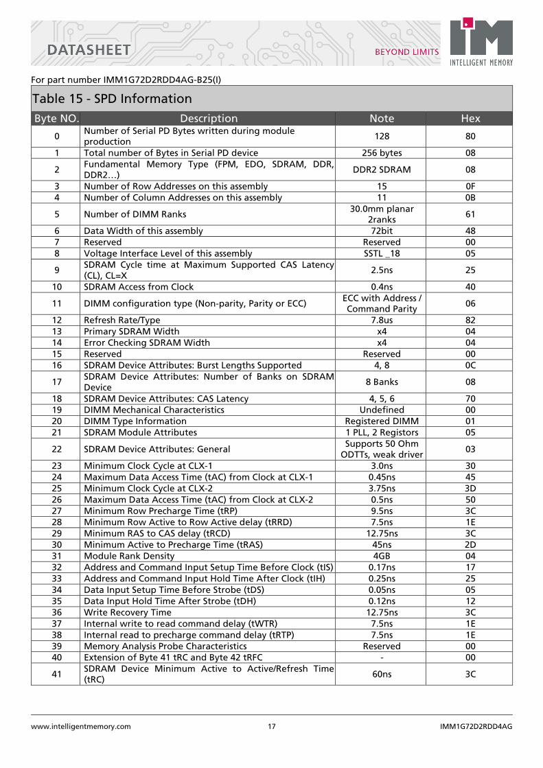
Table 15 - SPD Information
Byte NO. Description Note Hex
0 Number of Serial PD Bytes written during module production
128 80
1 Total number of Bytes in Serial PD device 256 bytes 08
2 Fundamental Memory Type (FPM, EDO, SDRAM, DDR, DDR2…)
DDR2 SDRAM 08
3 Number of Row Addresses on this assembly 15 0F 4 Number of Column Addresses on this assembly 11 0B
5 Number of DIMM Ranks 30.0mm planar
2ranks 61
6 Data Width of this assembly 72bit 48 7 Reserved Reserved 00 8 Voltage Interface Level of this assembly SSTL _18 05
9 SDRAM Cycle time at Maximum Supported CAS Latency (CL), CL=X
2.5ns 25
10 SDRAM Access from Clock 0.4ns 40
11 DIMM configuration type (Non-parity, Parity or ECC) ECC with Address / Command Parity
06
12 Refresh Rate/Type 7.8us 82 13 Primary SDRAM Width x4 04 14 Error Checking SDRAM Width x4 04 15 Reserved Reserved 00 16 SDRAM Device Attributes: Burst Lengths Supported 4, 8 0C
17 SDRAM Device Attributes: Number of Banks on SDRAM Device
8 Banks 08
18 SDRAM Device Attributes: CAS Latency 4, 5, 6 70 19 DIMM Mechanical Characteristics Undefined 00 20 DIMM Type Information Registered DIMM 01 21 SDRAM Module Attributes 1 PLL, 2 Registors 05
22 SDRAM Device Attributes: General Supports 50 Ohm
ODTTs, weak driver 03
23 Minimum Clock Cycle at CLX-1 3.0ns 30 24 Maximum Data Access Time (tAC) from Clock at CLX-1 0.45ns 45 25 Minimum Clock Cycle at CLX-2 3.75ns 3D 26 Maximum Data Access Time (tAC) from Clock at CLX-2 0.5ns 50 27 Minimum Row Precharge Time (tRP) 9.5ns 3C 28 Minimum Row Active to Row Active delay (tRRD) 7.5ns 1E 29 Minimum RAS to CAS delay (tRCD) 12.75ns 3C 30 Minimum Active to Precharge Time (tRAS) 45ns 2D 31 Module Rank Density 4GB 04 32 Address and Command Input Setup Time Before Clock (tIS) 0.17ns 17 33 Address and Command Input Hold Time After Clock (tIH) 0.25ns 25 34 Data Input Setup Time Before Strobe (tDS) 0.05ns 05 35 Data Input Hold Time After Strobe (tDH) 0.12ns 12 36 Write Recovery Time 12.75ns 3C 37 Internal write to read command delay (tWTR) 7.5ns 1E 38 Internal read to precharge command delay (tRTP) 7.5ns 1E 39 Memory Analysis Probe Characteristics Reserved 00 40 Extension of Byte 41 tRC and Byte 42 tRFC - 00
41 SDRAM Device Minimum Active to Active/Refresh Time (tRC)
60ns 3C
www.intelligentmemory.com 18 IMM1G72D2RDD4AG
Byte NO. Description Note Hex
42 SDRAM Device Minimum Refresh to Active/Refresh Command Period (tRFC)
195ns C3
43 SDRAM Device Maximum device cycle time (tCKmax) 8.0ns 80
44 SDRAM Device maximum skew between DQS and DQ signals (tDQSQ)
0.20ns 14
45 SDRAM Device Maximum Read Data Hold Skew Factor (tQHS)
0.30ns 1E
46 PLL Relock Time 15us 0F
47 Bits 7:4: Tcasemax, Bits 3:0: DT4R4W Delta Tcasemax = 85oC
Not support DT4R4W Delta
00
48 Thermal resistance of DRAM device package from top (case) to ambient (Psi T-A DRAM)
Not supported 00
49 DRAM Case Temperature Rise from Ambient due to Activate-Precharge/Mode Bits (DT0/Mode Bits)
Not defined 00
50 DRAM Case Temperature Rise from Ambient due to Precharge/Quiet Standby (DT2N/DT2Q)
Not supported 00
51 DRAM Case Temperature Rise from Ambient due to Precharge Power-Down(DT2P)
Not supported 00
52 DRAM Case Temperature Rise from Ambient due to Active Standby (DT3N)
Not supported 00
53 DRAM Case temperature Rise from Ambient due to Active Power-Down with Fast PDN Exit (DT3Pfast)
Not supported 00
54 DRAM Case temperature Rise from Ambient due to Active Power-Down with Slow PDN Exit (DT3Pslow)
Not supported 00
55 DRAM Case Temperature Rise from Ambient due to Page Open Burst Read/ DT4R4W Mode Bit (DT4R/DT4R4W Mode Bit)
Not supported 00
56 DRAM Case Temperature Rise from Ambient due to Burst Refresh (DT5B)
Not supported 00
57 DRAM Case Temperature Rise from Ambient due to Bank Interleave Reads with Auto-Precharge (DT7)
Not supported 00
58 Thermal Resistance of PLL Package from Top (Case) to Ambient ( Psi T-A PLL )
Not supported 00
59 Thermal Resistance of Register Package from Top (Case) to Ambient ( Psi T-A Register)
Not supported 00
60 PLL Case Temperature Rise from Ambient due to PLL Active (DT PLL Active)
Not supported 00
61 Register Case Temperature Rise from Ambient due to Register Active/Mode Bit (DT Register Active/Mode Bit)
Not supported 00
62 SPD Revision 1.3 13 63 Checksum for Bytes 0-62 - 41
64-71 Manufacturer’s JEDEC ID Code Reserved Reserved 72 Module Manufacturing Location Reserved Reserved
73-90 Module Part Number Reserved Reserved 91-92 Module Revision Code Reserved Reserved 93-94 Module Manufacturing Date Reserved Reserved 95-98 Module Serial Number Reserved Reserved 99-127 Manufacturer’s Specific Data Reserved Reserved 128-255 Open for customer use Reserved Reserved
www.intelligentmemory.com 19 IMM1G72D2RDD4AG
Revision History
Revision Descriptions Release Date
1.0 Initial release Sep, 2019
www.intelligentmemory.com 20 IMM1G72D2RDD4AG
Contents
Features 2
Table 1 - Ordering Information for RoHS Compliant Product 3
Table 2 - Temperature Grade 3
Table 3 - Speed Grade 3
Table 4 - Memory Chip Information 3
Part Number Decoder 4
Table 5 - Addressing 4
Table 6 - Pin Assignment 5
Table 7 - Pin Description 6
Module Dimension 7
Figure 1 – 240 Pin DDR2 SDRAM Registered DIMM 7
Table 8 - PCB Dimension 7
Figure 2 – Functional Block Diagram (Page 1 of 3) 8
Figure 3 – Functional Block Diagram (Page 2 of 3) 9
Figure 4 – Functional Block Diagram (Page 3 of 3) 10
Electrical Parameter 11
Table 9 – Absolute Maximum DC Ratings 11
Table 10 - DC Electrical Characteristics and Operating Conditions 12
Table 11 - Input Switching Conditions 12
Table 12 - Differential Input and Output Operating Conditions (CK, /CK and DQS, /DQS) 12
Table 13 - IDD Specifications with Conditions and Operation Current 13
Table 14 - AC Timing Parameter and Operating Conditions 14
Table 15 - SPD Information 17
Revision History 19
Contents 20
List of Tables 21
List of Figures 21
www.intelligentmemory.com 21 IMM1G72D2RDD4AG
List of Tables
Table 1 - Ordering Information for RoHS Compliant Product 3
Table 2 - Temperature Grade 3
Table 3 - Speed Grade 3
Table 4 - Memory Chip Information 3
Table 5 - Addressing 4
Table 6 - Pin Assignment 5
Table 7 - Pin Description 6
Table 8 - PCB Dimension 7
Table 9 – Absolute Maximum DC Ratings 11
Table 10 - DC Electrical Characteristics and Operating Conditions 12
Table 11 - Input Switching Conditions 12
Table 12 - Differential Input and Output Operating Conditions (CK, /CK and DQS, /DQS) 12
Table 13 - IDD Specifications with Conditions and Operation Current 13
Table 14 - AC Timing Parameter and Operating Conditions 14
Table 15 - SPD Information 17
List of Figures
Figure 1 – 240 Pin DDR2 SDRAM Registered DIMM 7
Figure 2 – Functional Block Diagram (Page 1 of 3) 8
Figure 3 – Functional Block Diagram (Page 2 of 3) 9
Figure 4 – Functional Block Diagram (Page 3 of 3) 10


![DDR3 72 bit ECC UNB SODIMM Low Voltage VR7PUxx7298xxx Sheets/Viking PDFs... · Module Configuration ... 10/AP,9:0] IN determine whether ... 72 bit ECC UNB SODIMM Low Voltage VR7PUxx7298xxx](https://img.pdfslide.us/doc/110x75/5a70723c7f8b9a9d538bfa15/ddr3-72-bit-ecc-unb-sodimm-low-voltage-vr7puxx7298xxx-sheetsviking-pdfspdf.jpg)