Embed Size (px)
Citation preview
IMD - Software for modeling the optical properties of multilayer
films
David L. Windt
Bell Laboratories
Room 1D-456, 600 Mountain Ave.
Murray Hill, NJ 07974
www.bell-labs.com/user/windt
To be published in
Computers In Physics
Jul/Aug 1998
1
IMD - Software for modeling the optical properties of multilayer
films
David L. Windt
Bell Laboratories
Room 1D-456, 600 Mountain Ave.
Murray Hill, NJ 07974
www.bell-labs.com/user/windt
Abstract
A computer program called IMD is described. IMD is used for modeling the optical properties
(reflectance, transmittance, electric field intensities, etc.) of multilayer films, i.e., films consisting of any
number of layers of any thickness. IMD includes a full graphical user interface, and affords modeling
with up to eight simultaneous independent variables, as well as parameter estimation (including
confidence interval generation) using non-linear, least-squares curve fitting to user-supplied experimental
optical data. The computation methods and user interface are described, and a number of examples are
presented which illustrate some of IMD’s unique modeling, fitting and visualization capabilities.
Keywords: multilayer films, optical modeling, parameter estimation.
2
1. Introduction
IMD is a computer program for modeling the optical properties reflectance, transmittance,
absorptance, phase shifts and electric field intensities of multilayer films, i.e., films consisting of any
number of layers of any thickness. Estimating the optical properties of multilayer films is integral to
instrument design and modeling in many fields of science and technology, such as astronomy,
lithography, plasma diagnostics, synchrotron instrumentation, etc. Also, fitting the calculated reflectance
of a multilayer stack to experimental data is the basis of X-Ray Reflectance (XRR) analysis of thin films,
where one uses the measured reflectance to determine film thicknesses, densities, and roughnesses, and to
optical constant determination from reflectance vs. incidence angle data, a technique utilized in many
spectral regions.1 IMD was designed, therefore, as a completely general modeling and parameter
estimation tool, intended to be used for these and other applications, in order to meet the needs of a broad
range of researchers. Furthermore, IMD’s flexibility enables many new and unique types of computations.
IMD is available for free via the Internet.2
In IMD, a layer can be composed of any material for which the optical constants are known or
can be estimated. Any number of such layers can be designated and optionally grouped together to
define periodic multilayers; ‘groups of groups’ of layers can be defined, in fact, with no limit on nesting
depth. The IMD distribution includes an optical constant database for over 150 materials, spanning the X-
ray to the far infrared region of the spectrum. User-defined optical constants can be used as well, and in
the 30 eV to 30 keV region in particular, optical constants can be generated by the user for arbitrary
compounds using the CXRO atomic scattering factors.3 Imperfections at an interface, i.e., roughness
and/or diffuseness, can be easily included; the effect of such imperfections, namely, to reduce the specular
reflectance at the interface, becomes especially important at shorter wavelengths (i.e., below ~30 nm),
where the length scale of these imperfections is comparable to the wavelength of light.
The optical functions (reflectance, transmittance, etc.) can be computed not just versus
wavelength and/or incidence angle, but also as a function of any of the parameters that describe the
multilayer stack (e.g., layer thicknesses, roughnesses, etc.) or the incident beam (polarization,
3
angular/spectral resolution.) An interactive visualization tool, IMDXPLOT, is used to display the results
of such multiple-variable computations; with this visualization tool one can vary a given parameter and
see the resulting effect on the optical functions (in one or two dimensions) in real time. This last feature
is especially helpful in discerning the relative sensitivities of the optical functions to the parameters that
describe the multilayer structure.
Parameter estimation is afforded by fitting an optical function to user-supplied experimental data:
non-linear, least-squares curve fitting based on the χ2 test of fit is utilized. The precision of the best-fit
parameters can be estimated as well, by computing multi-dimensional confidence intervals. The ability to
simultaneously vary multiple parameters ‘manually’, as mentioned above, prior to performing least-
squares fitting, is particularly useful in selecting initial parameter values; indeed choosing initial fit
parameter values that are reasonably close to the best-fit values is generally the most difficult aspect of
multi-parameter non-linear fitting.
IMD is written in the IDL language,4 and makes extensive use of IDL’s built-in ‘widgets’ to
provide a full graphical user interface (GUI.) As such, IMD can be run on most (currently) popular
platforms, including MacOS, MS Windows, and most flavors of Unix.
In the following sections, I will describe first the physics and algorithms used for modeling and
parameter estimation, followed by a description of the IMD user interface. Finally, I present several
illustrative examples, demonstrating IMD’s unique modeling and fitting capabilities.
2. Computation Methods
2.1 Optical Functions
Computations of the optical functions of a multilayer film in IMD are based on application of the
Fresnel equations, modified to account for interface imperfections, which describe the reflection and
transmission of an electromagnetic plane wave incident at an interface between two optically dissimilar
materials.
4
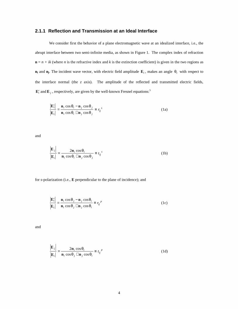
2.1.1 Reflection and Transmission at an Ideal Interface
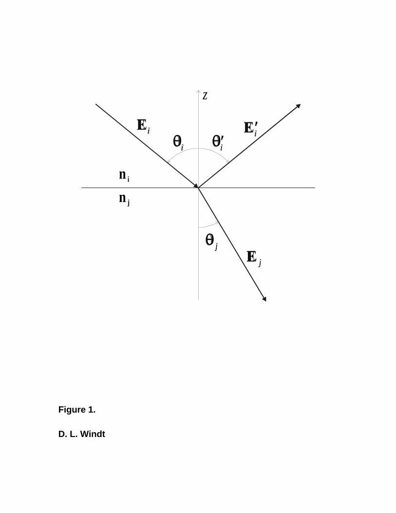
We consider first the behavior of a plane electromagnetic wave at an idealized interface, i.e., the
abrupt interface between two semi-infinite media, as shown in Figure 1. The complex index of refraction
n = n + ik (where n is the refractive index and k is the extinction coefficient) is given in the two regions as
ni and nj. The incident wave vector, with electric field amplitude Ei , makes an angle θi with respect to
the interface normal (the z axis). The amplitude of the reflected and transmitted electric fields,
′Ei andE j , respectively, are given by the well-known Fresnel equations:5
′=
−
+≡
E
E
n n
n n
i
i
i i j j
i i j jij
srcos cos
cos cos
θ θ
θ θ(1a)
and
E
E
n
n n
j
i
i i
i i j jij
st=+
≡2 cos
cos cos
θθ θ
(1b)
for s-polarization (i.e., E perpendicular to the plane of incidence); and
′=
−+
≡E
E
n n
n ni
i
i j j i
i j j iij
prcos cos
cos cos
θ θθ θ
(1c)
and
E
E
n
n n
j
i
i i
i j j iij
pt=+
≡2 cos
cos cos
θθ θ
(1d)
5
for p-polarization (i.e., E parallel to the plane of incidence), where θ j is the angle of refraction,
determined from Snell’s law: n ni i j jsin sinθ θ= . In equation (1) we have introduced the Fresnel
reflection and transmission coefficients, rij and tij , respectively.6
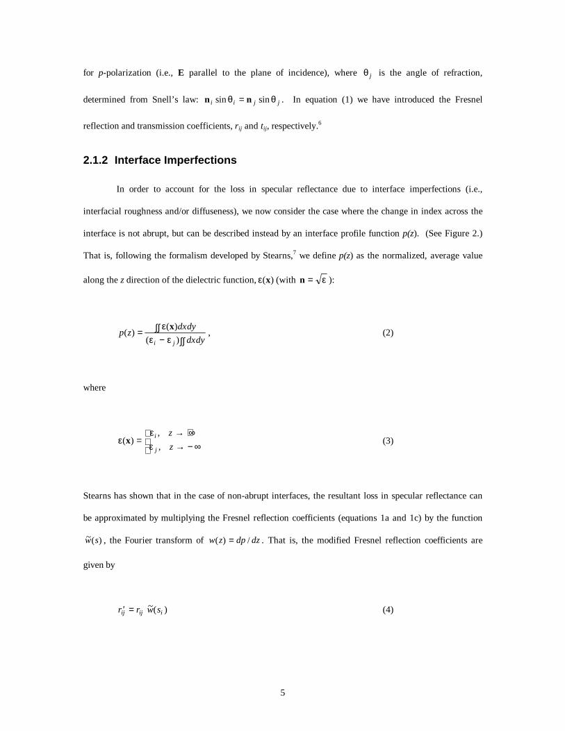
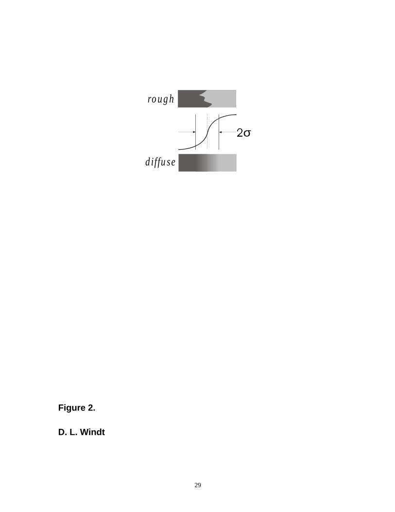
2.1.2 Interface Imperfections
In order to account for the loss in specular reflectance due to interface imperfections (i.e.,
interfacial roughness and/or diffuseness), we now consider the case where the change in index across the
interface is not abrupt, but can be described instead by an interface profile function p(z). (See Figure 2.)
That is, following the formalism developed by Stearns,7 we define p(z) as the normalized, average value
along the z direction of the dielectric function,ε( )x (with n = ε ):
p zdxdy
dxdyi j
( )( )
( )= ∫∫
− ∫∫ε
ε εx
, (2)
where
εεε
( ),
,x =
→ + ∞→ − ∞
i
j
z
z(3)
Stearns has shown that in the case of non-abrupt interfaces, the resultant loss in specular reflectance can
be approximated by multiplying the Fresnel reflection coefficients (equations 1a and 1c) by the function
~( )w s , the Fourier transform of w z dp dz( ) /= . That is, the modified Fresnel reflection coefficients are
given by
′ =r r w sij ij i~( ) (4)
6
where si i= 4π θ λcos / , andλ is the wavelength of light. Note that the loss in specular reflectance
depends only on the average variation (over x and y) in index across the interface. Consequently, the
reflectance can be reduced equally well by either a rough interface, in which the transition between the
two materials is abrupt at any point (x,y), or a diffuse interface, in which the index varies smoothly along
the z direction (or by an interface that can be described as some combination of the two cases.)
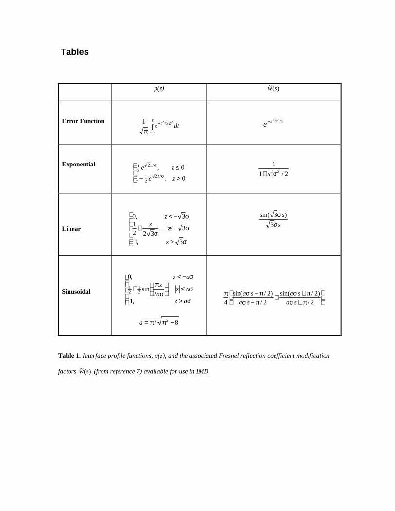
Stearns presents four particularly useful interface profiles, all of which are available for use in
IMD; these interface profile functions and the associated ~( )w s functions are listed Table 1. Also available
in IMD are modified~( )w s functions, wheresi has been replaced with sij i j= 4π θ θ λcos cos / , in accord
with the formalism developed by Névot and Croce8 to properly account for the effect of roughness on the
specular reflectance below the critical angle of total external reflection in the X-ray region.
The width of each interface profile function presented in Table 1 is characterized by the
parameter σ (see Figure 2), which is a measure of either an rms interfacial roughness, in the case of a
purely rough interface, an interface width, in the case of a purely a diffuse interface, or some combination
of the two properties in the case of an interface that is both rough and diffuse; it is the parameter σ (along
with the choice of interface profile function) that is specified in IMD to account for the effects of interface
imperfections using the modified Fresnel coefficient approach just described.
2.1.3 Optical Functions of a Multilayer Stack
We now consider a plane wave incident on a multilayer stack, that is, a series of N layers (and
N+1 interfaces), where the i th layer has thickness di, interfacial roughness/diffuseness σi, and optical
constants ni, as shown in Figure 3. The region above the multilayer stack the ambient has optical
constants na, and the region below the film the substrate has optical constants ns. (Note that the case
of a free-standing film refers to the condition ns = na.) Under these circumstances, the net reflection (ri)
and transmission (ti) coefficients of the i th layer are given by:9
7
rr r e
r r ei
ij ji
ij ji
i
i=
+
+
2
21
β
β (5a)
and
tt t e
r r ei
ij ji
ij ji
i
i=
+
2
21
β
β (5b)
where β π θ λi i i id= 2 n cos / ; the reflection coefficients rij are computed from equation (4), the
transmission coefficients tij from equations (1b) and (1d), and rj and tj are the net reflection and
transmission coefficients of the j th interface. Thus, the procedure to compute the net reflection (r) and
transmission (t) coefficients for the multilayer stack is to apply equation (5) recursively, starting at the
bottom-most layer, i.e., i = N, j = s. (The coefficients r and t for s- and p-polarization are computed
separately, using the appropriate Fresnel coefficients.) The reflectance, R and transmittance, T, which
measure the energy reflected from or transmitted through the film, respectively, are then given by
R r= 2(6a)
and
T ts s
a a
=
Recos
cos
n
n
θθ
2(6b)
(again, computing separately the values for s- and p-polarization, i.e., Rs, Rp, Ts, and Tp.) The absorptance,
A, which measures the amount of energy absorbed by the film, is approximated by
8
A R T= − −1 (6c)
(Note that equation (6c) is inaccurate when light is removed from the specular direction, i.e., and scattered
into non-specular directions, due to interfacial or surface roughness.) Finally, the phases of the reflected
and transmitted waves are given by:
φr r r= −tan (Im{ } / Re{ })1 (7a)
and
φt t t= −tan (Im{ } / Re{ })1 (7b)
2.1.4 Electric Field Intensity in a Multilayer Stack
In order to compute, in addition to the optical functions, the electric field intensity as a function
of depth in a multilayer stack, a slightly different formalism from that described in the previous section
must be used. (The previous, more efficient, formalism is used in IMD when electric field intensities are
not required.) Consider the interface between the i th and the j th layers in a multilayer stack, where we now
have both positive-going and negative-going electromagnetic plane waves in both layers. Solving
Maxwell’s equations in this case, it can be shown that the positive-going and negative-going field
amplitudes at a distance zi above the interface are given by
E zt
e Er
te Ei i
ij
i zj
ij
ij
i zj
i i i i+ − + − −= +( ) ( ) ( )( ) ( )10 0β β (8a)
and
E zr
te E
te Ei i
ij
ij
i zj
ij
i zj
i i i i− + −= +( ) ( ) ( )( ) ( )β β01
0 (8b)

9
respectively, where β π θ λi i i i iz z( ) cos /= 2 n , and E j+ ( )0 and E j
− ( )0 are the field amplitudes at the top
of the j th layer. Again, a recursive approach can be used to compute the field amplitudes throughout the
stack, starting at the bottom-most layer (i = N, j = s) with the field amplitudes in the substrate given as
Es+ =( )0 1 and Es
− =( )0 0 . The net reflection and transmission coefficients of the film can then be
computed from the field amplitudes in the ambient:
rE
Ea
a=
−
+( )
( )
0
0(9a)
and
tEa
= +1
0( )(9b)
Once the transmission coefficient is computed from equation (9b), the field amplitudes versus depth are
then re-scaled using
E z tE z± ±→( ) ( ) , (10)
(i.e., taking the incident electric field to have unit amplitude) and the field intensities for s- and p-
polarization computed from
I z E z E z( ) ( ) ( )= ++ − 2(11)
10
2.1.5 Polarization
In the case of an incident beam that consists of a mixture of s- and p-polarization, it is often
necessary to compute the ‘average’ values of the optical functions R, T, and A, and the electric field
intensity I, i.e., the values of these quantities for ‘average’ polarization. We thus define the incident
polarization factor f as
fI I
I I
s p
s p=
−+
, (11)
whereI sandI p
are the incident intensities for s- and p-polarization (e.g., unpolarized radiation
corresponds to f = 0.) Furthermore, we define the polarization analyzer sensitivity, q, as the sensitivity to
s-polarization divided by the sensitivity to p-polarization; specifying a value of q other than 1.0 could be
used to simulate, for example, the reflectance one would measure using a detector that (for whatever
reason) was more or less sensitive to s-polarization than to p-polarization. It can be shown that the
average reflectance is then given by
RR q f R f
f q qa
s p
=+ + −
− + +( ) ( )
( ) ( )
1 1
1 1, (12)
with equivalent expressions for Ta, Aa and Ia.
2.1.6 Instrumental Resolution
In general, the experimental determination of an optical function such as R, T or A is made with
instrumentation that is limited in angular and/or spectral resolution. As such, it is desirable to estimate
resolution-limited values of the calculated optical functions. This is achieved in IMD by convolving the
calculated optical functions with a Gaussian of width δθ, in the case of finite angular resolution, or with a
11
Gaussian of width δλ in the case of finite spectral resolution, using the convolution algorithm built into
IDL.
2.1.7 Graded Interfaces
In addition to the option of using the modified Fresnel coefficients to account for interfacial
roughness and diffuseness, as described in Section 2.1.2, in IMD it’s also possible to model the effects of
a diffuse interface on the optical functions and electric field intensities by specifying a ‘graded’ interface.
That is, an abrupt interface can be replaced by one or more layers whose optical constants vary gradually
between the values for the pure materials on either side of the interface.
In IMD, a graded interface is described by three parameters, as shown in Figure 4: the interface
width, wg, the number of layers comprising the graded interface, Ng, and the distribution factor, Xg, which
determines where the graded interface region resides relative to the original abrupt interface (as will be
described below.)
The optical constants in each of the Ng layers of a graded interface are computed as follows.
Consider the graded interface between the i th and j th layers in a multilayer stack. The thickness of each of
the Ng graded interface layers is equal to wg / Ng. The optical constants in the �th graded interface layer
are thus given by
nN n n
N
g i j
g�
� �
=+ − +
+( )
( )
1
1(13a)
and
kN k k
N
g i j
g�
� �=
+ − ++
( )
( )
1
1(13b)
12
with � �= 1, Ng . The resulting layer thicknesses, ′di and ′d j , of the pure materials in the i th and j th
layers, respectively, after including the graded interface layers, are given by
′ = − −d d w Xi i g g( )1 (14a)
and
′ = −d d w Xj j g g (14b)
with 0 1< <Xg . (Note that the total thickness of the two layers — including all the graded interface
layers — is constant, i.e., ′ + ′ + = +d d w d di j g i j .) As an example, a distribution factor of 50%
( X g = 05. ) would result in equal reductions of the i th and j th layer thicknesses.
2.2 Parameter Estimation
As will be described in section 3.2, it is possible in IMD to designate simultaneously up to eight
independent variables when computing optical functions and electric field intensities. When attempting
to model experimental optical data, however, it is often desirable to estimate parameter values
automatically, using nonlinear, least-squares curve-fitting. To this end, parameter estimation based on the
χ2 test of fit can be used in IMD to determine any number of parameters that describe the multilayer stack
(or the incident beam polarization and/or instrumental resolution), as will now be described.
2.2.1 Fitting Algorithm
Consider a one-dimensional optical function Y X( ) for a multilayer stack, where Y may be any
one of R Ta a, or Aa , and X is some independent variable (e.g., λ, θ, etc.) The values for Y X( ) depend
on the values of all of the parameters that describe the multilayer stack (optical constants, layer
thicknesses, etc.) and the incident beam (polarization, instrumental resolution, etc.). The problem we wish
13
to solve is the following: determine the values for some fixed number p of these adjustable parameters,
such that the calculated optical function Y X( ) most closely fits a particular set of experimentally-
determined optical data, Y Ym m± δ , measured as a function of the independent variable Xm , where Xm
takes on i Nm= 1,� discrete values.
To solve this problem, IMD makes use of the so-called Marquardt gradient-expansion
algorithm,10 based on the χ2 test,11 in which we minimize the value of the statistic S, defined as
SY i Y i
w im
i
Nm
≡−
∑=
( [ ] [ ])
[ ]
2
21
, (15)
where w[i] are the weighting factors for each point. IMD uses the CURVEFIT procedure,11 an adaptation
of the Marquardt algorithm included in the IDL library. The user designates adjustable parameters, and
initial values for each. (In IMD, a constraint on the range of acceptable parameter values can be specified
as well.) Iterations are then performed until the change in S is less than a specified amount, or until a
maximum number of iterations have been performed. The user can choose to use for w[i] either (a)
‘instrumental weighting,’ using the experimental uncertainties, w i Y im[ ] [ ]= δ , (b) ‘statistical weighting,’
with w i Y im[ ] [ ]= , or (c) ‘uniform weighting,’ withw i[ ] = 1. Additionally, logarithmic fitting can be
used, in which the numerator in equation (15) is replaced by (ln [ ] ln [ ])Y i Y im− 2 .
2.2.2 Confidence Interval Computation
In addition to a point estimate determination of the ‘best-fit’ parameter values, using the fitting
technique just described, for example, it is generally necessary to estimate also the range of acceptable
parameter values that are consistent with the experimental data. To this end, in IMD it is possible to
compute multi-dimensional confidence intervals associated with the best-fit values of the adjustable
parameters, using the formalism described in references 12 and 13.
14
It can be shown that when using the χ2 test of fit, the minimum value of the S statistic, Smin ,
associated with the best-fit parameter values, is distributed as the χ2 probability function with
N pm − degrees of freedom:
S N pmmin ( )= −χ α2 , (16)
where α is the significance of fit. That is, if we find, for example, that S N pmmin ( . )= −χ2 0 68 , then we can
conclude that there is a 68% probability that the model (using the p best-fit parameter values) correctly
describes the data.
The confidence region, with significance ′α , is then defined as the p-dimensional region of
parameter space for which the value of S is less than or equal to some value SL, where
S S SL = + ′min ( )∆ α , (17)
with ∆S( )′α equal to the value of the χ2 probability function with p degrees of freedom and significance
′α ; the confidence region so defined would enclose the true values of the p parameters in 1− ′α of all
experiments.
In IMD, a multi-dimensional confidence region can be determined for up to eight adjustable (i.e.,
fit) parameters simultaneously. In this case a grid-search algorithm is utilized, wherein the user specifies
the extent and resolution of the grid along each parameter axis. At each point in the grid, the value of the
statistic S is computed using one of two methods, depending on the dimensionality of the confidence
region being determined. That is, suppose the best-fit parameters were determined by varying p adjustable
parameters, as described above, and of these p parameters we are interested in the confidence region
associated with some subset of parameters q, where q p≤ . In the case that q = p, the value of S at each
point on the grid is determined directly from equation (15). On the other hand, in the case that q < p, the
value of S at each point on the grid is determined in IMD using the minimization algorithm described in
15
the previous section, but with only (p - q) adjustable parameters, i.e., q of the parameters are now fixed.
In this case, we note that the correct value of ∆S( )′α to be used in equation (17) is equal to the value of
the χ2 probability function with q (not p) degrees of freedom and significance ′α . As an example of a
situation for which q < p, consider the case of making a determination of thin film optical constants from
reflectance vs. incidence angle data, where three adjustable parameters have been used, say the optical
constants n and k, and the film thickness, d but of these three parameters, we are interested only in the
uncertainty on the derived values of n and k, and so we must compute the associated 2-dimensional
confidence region in n-k space. A specific example of a confidence interval computation which illustrates
the concepts described here will be presented in Section 4.4.
3. User Interface
I now describe the IMD graphical user interface (GUI). This interface, which is created from the
widgets tool kit built into IDL, is used to specify all parameters and variables, and to visualize the results
of all calculations.
Shown in Figure 5 is the main IMD widget as it might look after a periodic multilayer and
associated independent and dependent variables have been specified. In addition to the menu bar at the
top of the widget, there are three regions of this widget of particular interest to us now: the STRUCTURE
region, and the INDEPENDENT and DEPENDENT VARIABLES regions.
3.1 Structure Specification
The first step in performing a calculation in IMD is defining the ‘structure’, i.e., the parameters
that define the ambient material, the multilayer stack, and (optionally) a substrate. There are a number of
parameters that can be assigned to each structure element, i.e., layer thicknesses, interface
roughness/diffuseness parameters, etc. But common to all structure elements is the material designation,
which determines which optical constants are used for the calculation, as described in the next section.
16
3.1.1 Material Designation
Each structure element - the ambient, the substrate, and each multilayer stack layer element - is
composed of some material. There are two different methods available to the user to designate materials in
IMD: in the first method, the designated material name refers to an optical constants file contained in the
IMD optical constant database; in the second method, which is applicable only in the X-ray region for
energies between 30 eV and 30 keV, the material is specified by its composition and density, and the
optical constants are computed directly from the atomic scattering factors.
The IMD optical constants database is a directory of ASCII files, where each optical constants
file contains three columns of optical data (λ, n and k) associated with a single material. To designate a
material by reference to an optical constants file, the user need only specify a valid file name contained in
the optical constants directory. For example, shown in Figure 6(a) is a typical IMD layer widget where the
material has been designated as amorphous Al2O3, i.e., corresponding to a file called ‘a-Al2O3.nk’.
The IMD optical constants database contains data for over 150 materials, compiled from a variety
of published sources, with wavelength coverage extending from the X-ray to the far infrared region of the
spectrum. In order to use additional optical constants, a user need only create an ASCII file containing the
optical constants for the desired material, in accord with a simple format specified in the IMD
documentation. For many materials, the user can choose from among several data sets already available
in the database. The contents of any of the files contained in the database can be displayed graphically
using an interactive plot widget, available through a pull-down menu option from the main IMD widget.
The basis for the second method of material designation by composition and density is that
in the X-ray region, the complex index of refraction for a compound of density ρ is related to the atomic
scattering factors f1 and f2 by 3
n ≅ −+∑
∑1
2
2
22
1 2e N
m c
x f i f
x Aa
e
j j jj
j jj
πλ ρ
( ), ,
, (18)
17
where the sums range over each of the chemical elements that comprise the compound, the xj are the
relative concentrations of each element, and the Aj are the associated atomic densities; e, me, c, and Na are
the electron charge, the electron mass, the speed of light, and Avogadro’s number, respectively. To utilize
this method of material designation, the user must specify the atomic composition (i.e., the xj) and the
density of the material, as illustrated in Figure 6(b), for example, showing the layer widget for a layer
composed of Cr3C2 having a density of 6.68 gm/cm3.
3.1.2 Layer and Group Parameters
To create an IMD structure, the user adds layers, periodic multilayers,14 and optionally a
substrate as desired. Accomplishing these tasks is simply a matter of pushing the appropriate buttons on
the main IMD widget (i.e., on the right side of the STRUCTURE area of the widget shown in Figure 5.)
Layers and periodic multilayers can be subsequently grouped together to form higher level periodic
multilayers (with no limit on nesting depth), and can be moved up or down in the stack, again by pushing
the appropriate buttons. The structure components are listed on the main IMD widget (on the left side);
by double-clicking on a structure element, the associated ambient, layer, multilayer, or substrate widget is
created, allowing the user to specify adjustable parameters (e.g., materials, layer thicknesses, interface
parameters, multilayer repeat periods, etc.), as well as the preferred units (i.e., Å, nm, µm, etc.), and the
displayed precision of parameter values. Thus, rather complicated structures can be defined or changed
quickly and with relative ease.
3.2 Variable Designation
For all calculations, at least one wavelength (or energy) and incidence angle must be specified;
multiple wavelengths and/or angles can be specified as well, if desired. (In the case of electric field
intensity calculations, a third independent variable depth, i.e., the position in the structure, measured
from the top of the first layer must also be defined.) In addition to these variables, any of the
parameters that describe the multilayer stack (i.e., layer thicknesses, interface σ values, graded interface
parameters, multilayer parameters, etc.) or the incident beam (i.e., polarization parameters f and q, and
18
angular and spectral resolution) can be designated as independent variables; up to eight independent
variables can be designated simultaneously, and the dimensionality of the resulting optical functions will
be equal to the number of independent variables specified.
For every independent variable so designated, the user must define the extent and resolution of
the grid of points over which the optical functions are to be computed. The resolution of the grid can be
designated either by specifying the size of the increment between points, or by the total number of
parameter values that comprise the independent variable; Logarithmically spaced grids can also be
designated. The user can again specify the preferred precision and units, and in the case of wavelengths
(or energies) the instrumental resolution and polarization parameters; the angular instrumental resolution
is likewise specified using the incidence angle independent variable widget.
Once the structure and independent variables are defined, any or all of the optical functions R, T,
and A, and the electric field intensity I, can be computed, by selecting these functions in the
DEPENDENT VARIABLES area of the main IMD widget (see Figure 5.) By then choosing the
appropriate menu option, the computation is performed and the results displayed using another GUI tool,
IMDXPLOT. Specific examples illustrating the functionality of IMDXPLOT will be presented in
Section 4.
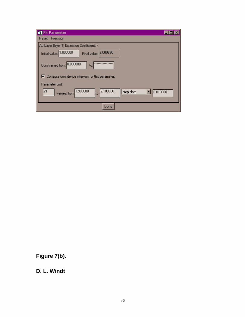
3.3 Fit Parameter Designation
As described in section 2.2, parameter estimation using non-linear, least-squares fitting can be
performed, utilizing user-supplied experimental data. The experimental data is read by accessing a menu
option from the main IMD widget, and the Parameter Estimation and Confidence Interval widget, shown
in Figure 7(a), allows the user to add and remove adjustable (fit) parameters, and to specify the
parameters that control how the fitting is performed (i.e., number of iterations, weighting, etc.) Shown in
Figure 7(b) is a typical Fit Parameter widget, wherein the user specifies the initial parameter value (and
optionally constraints on the fit parameter), as well as the parameters associated with confidence interval
computations, as described above in Section 2.2.2.
19
4. Examples
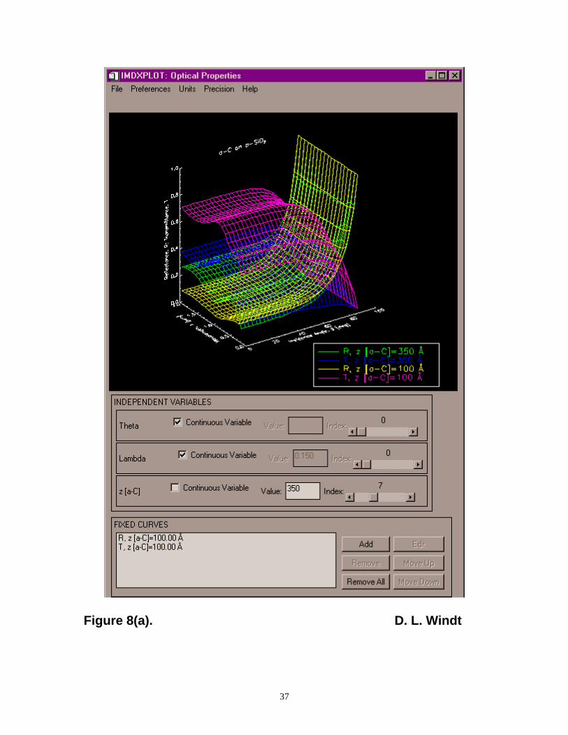
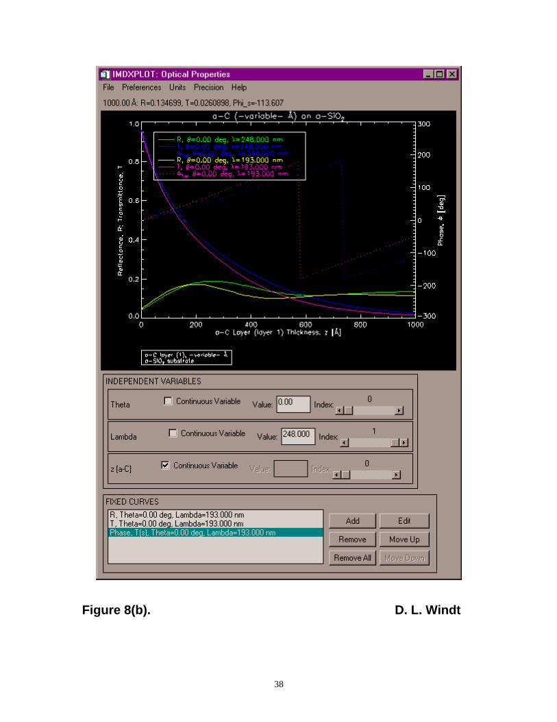
4.1 Multi-Dimensional Optical Functions of a Thin Film
The first example demonstrates how IMD can be used to visualize multi-dimensional optical
functions: I present the results of a computation of the reflectance and transmittance of an amorphous
carbon film15 on an amorphous SiO2 substrate, determined as a function of three independent variables:
wavelength, for 150 nm < λ < 2.0 µm, i.e., from the UV to the infrared; incidence angle, for 0° < θ < 90°;
and film thickness, for 0 Å < d < 1000 Å.
To visualize the results of this computation, one might imagine displaying one-dimensional
graphs of R and T, for example, as a continuous function of one variable, θ, say, and for discrete values of
λ and d. Or, perhaps it would be more useful to display a plot in two dimensions, as a continuous function
of two variables, and for discrete values of the remaining independent variable. The IMDXPLOT widget,
which is the interactive visualization tool in IMD, indeed allows the user to display such ‘slices’ of the
optical functions, in either one or two dimensions. For example, presented in Figure 8 are some of the
results of the computation just described. Figure 8(a) shows superposed 2-dimensional surface plots of
R (θ, λ) and T (θ, λ), for two discrete values of the film thickness, 100 Å and 350 Å. In Figure 8(b), on
the other hand, are 1-dimensional plots of R (d) and T (d), as well as the transmitted phase, φT(d), at
normal incidence, for two discrete wavelengths, 193 nm and 248 nm (i.e., the wavelengths used for DUV
lithography.) Using the buttons, sliders, and menu options available on the IMDXPLOT interface, the
user can easily display such slices through parameter space, and customize the graphs according to their
preference: multiple optical functions can be superposed, the appearance (i.e., colors, line-styles, plotting
symbols, etc.) of the different functions can be adjusted, and various legends and plot-labels can be
generated. Additionally, the sliders associated with each of the independent variables (shown in the
INDEPENDENT VARIABLES region of the IMDXPLOT widgets in Figure 8, for example) can be used
to vary in real time one or more independent variables and view the resulting effect on the optical
20
functions. A variety of standard graphics file formats (i.e., PostScript, PCL, HPGL, and CGM) are
available for output.
4.2 Reflectance and Electric Field Intensity for an X-Ray Multilayer Film
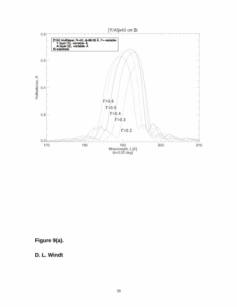
The second example shows how IMD can be used to adjust, for optimal performance, design
parameter values of a periodic multilayer. A determination of the electric field intensity in a periodic
multilayer film is presented as well. Shown in Figure 9(a) is an IMD-generated plot, showing the normal
incidence soft X-ray reflectance of a Y/Al periodic multilayer film (d=90 Å, N=40), as a function of one
particular design parameter, the film thickness ratio, Γ (where Γ ≡ +d d dY Y Al/ ( ) .) By using IMD to
compute R(Γ), the optimal value of Γ (i.e., giving the highest peak reflectance) is immediately evident.
Optimized values of other design parameters can be similarly obtained.
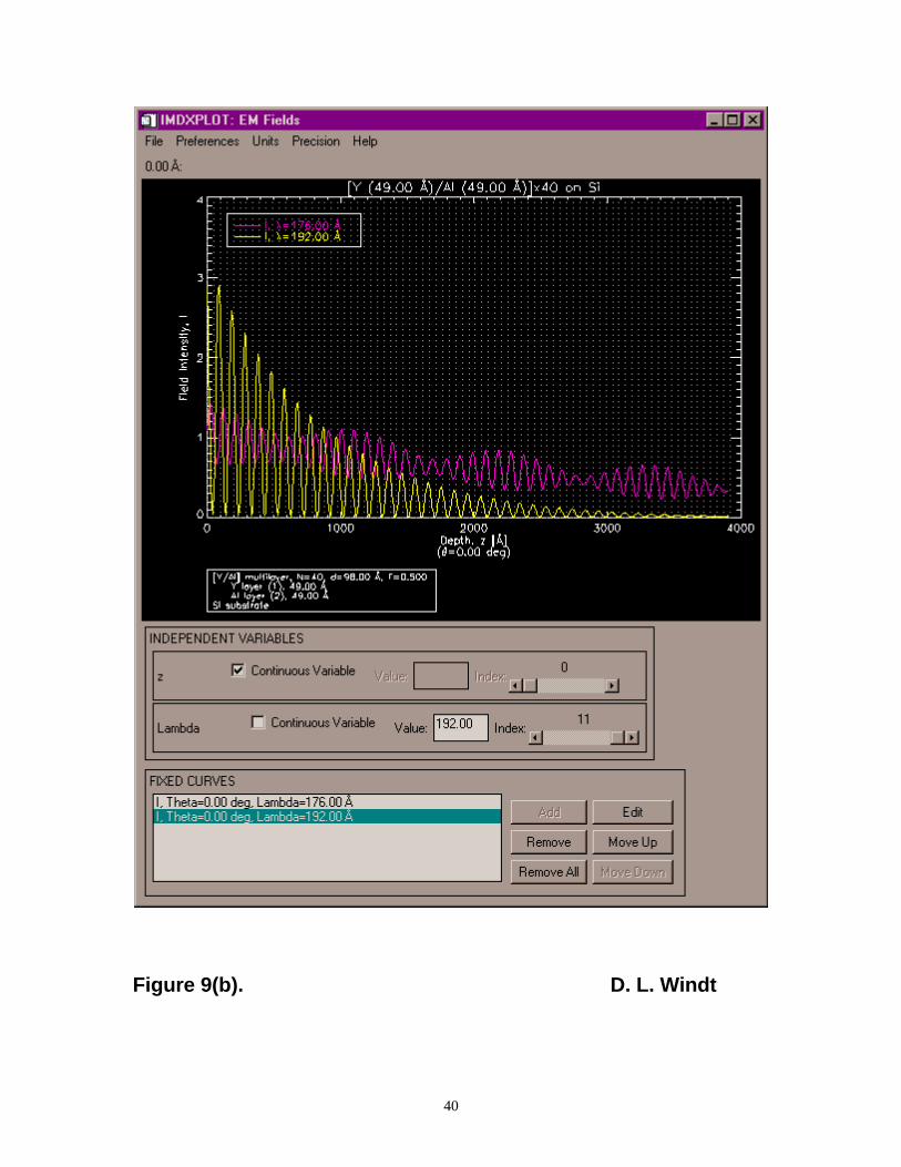
Displayed in Figure 9(b) is an IMDXPLOT widget showing the electric field intensity as a
function of depth for the Γ = 0.5 Y/Al multilayer, for two values of λ. An observation of the position of
the local maxima of the electric field intensity in the standing-wave pattern at λ=192 Å (i.e., the
wavelength corresponding to the peak reflectance) suggests, for example, that any interface imperfections
at the Al-on-Y interfaces, where the electric field intensity is strongest, might have a much different effect
on the peak reflectance than interface imperfections at the Y-on-Al interfaces, where the electric field
intensity is much weaker.
4.3 XRR Analysis of a W/Cr Bilayer
The third example demonstrates how the unique ability in IMD to interactively vary model
parameters ‘manually’ can be used, in conjunction with the non-linear, least-squares fitting capability, to
accurately determine a large number of film parameters from experimental data.
Shown in Figure 10 are the measured and calculated grazing incidence X-ray reflectance-vs.-
incidence-angle curves for a W/Cr bilayer thin film. These particular films are currently being used as the
electron scattering layers in masks for a projection electron-beam lithography tool currently being
developed16 (SCALPEL®,) in which the image contrast achieved at the focal plane of the tool depends
21
critically on the W and Cr layer thicknesses and densities. A precise measurement of these parameters is
thus required, and such a measurement can be obtained through the use of XRR analysis, using the curve-
fitting techniques described in Section 2.2. However, even for these relatively simple bilayer films, there
are a number of additional parameters in the model that must be varied in order to fit the data with
sufficient accuracy. For example, the best-fit curve shown in Figure 10 (labeled ‘σ=3.5 Å’) was obtained
by fitting eight adjustable parameters: the densities, layer thicknesses, and interface roughnesses of both
the W and Cr layers, as well as the thickness and roughness of a top layer oxide (WO3) that forms on
these films.
In order to utilize non-linear, least-squares curve-fitting to determine fit parameters, the choice of
initial parameter values must be relatively close to the final, ‘best-fit’ values, or else the fitting algorithm
will be unable to locate the global minimum in parameter space corresponding to the minimum value of
the χ2 statistic. This point is especially true in this particular example, where the fitting was performed
with so many adjustable parameters. The ability in IMD to first vary parameters ‘manually’ (as described
in Section 3.2) and to visualize in real-time the resulting effect on the optical functions (reflectance, in
this case), greatly facilitates the task of determining initial fit parameter values.
To illustrate, in order to fit the data shown in Figure 10, one might start (using bulk densities) by
manually varying the W and Cr layer thicknesses, until both the high-frequency and low-frequency
modulations in the calculated reflectance are reasonably coincident with those in the measured data.
These two superposed modulations (seen in Figure 10 as having periods of ~0.18° and ~1.0°,) correspond
to interference due to the total film thickness (i.e., WO3 + W + Cr layer thicknesses) and the Cr layer
thickness, respectively. Therefore, it’s especially useful to be able to manually vary two (or more) layer
thicknesses in a single calculation, and to view the results interactively using IMDXPLOT, in order to
match both modulations simultaneously. Nonetheless, the W and Cr layer thicknesses will generally need
significant refinement once other parameters are varied as well, as the effect on the reflectance of other
adjustable parameters are effectively coupled to the layer thicknesses. An example of such a coupling can
be seen in Figure 10, where reflectance curves are shown for several values of the W layer roughness: it
22
can be seen that the thickness modulations shift significantly with roughness (σ), an effect that cannot be
completely de-coupled from the effect of the individual layer thicknesses.
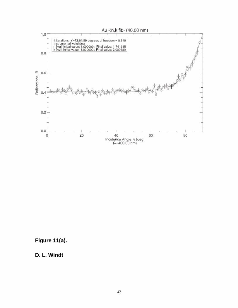
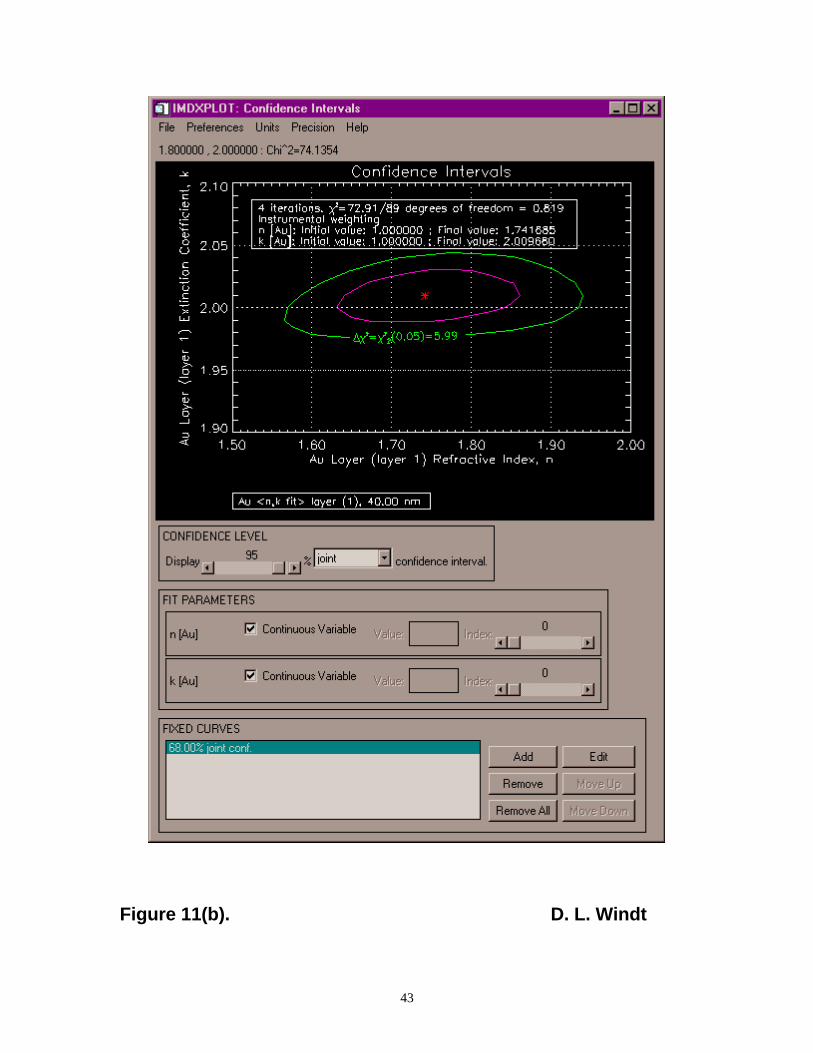
4.4 Optical Constants Determination for a Thin Film
The final example illustrates the ability in IMD to compute confidence intervals, in order to
estimate the precision of fit parameters determined from non-linear, least-squares curve-fitting. Shown in
Figure 11(a) are the results of non-linear, least-squares curve-fitting to determine, from reflectance vs.
incidence angle measurements, the optical constants (n and k) for a thin film. Once the best-fit
parameters were found (as indicated in Figure 11(a)), the value of the χ2 statistic S was computed over a
grid of points in parameter space, as described above in Section 2.2.2. The result of this computation are
displayed in the IMDXPLOT widget shown in Figure 11(b), where the contours-of-constant-S are shown
in two-dimensions, corresponding to the 68% (i.e., ‘1-σ’) and 95% (‘2-σ’) joint confidence regions. The
IMDXPLOT sliders in this case can be used to vary the value of ∆S( )′α (see equation 17), or to vary the
parameter values when displaying contours-of-constant-S in one dimension (not shown.)
5. Summary
I have described the physics and algorithms on which the IMD computer program is based, and
have presented a number of examples that illustrate some of IMD’s unique capabilities. Future
enhancements to IMD’s capabilities will include the ability to compute the non-specular (diffuse) scattered
intensity due to interfacial roughness, the ability to define depth-graded thicknesses and interface
parameters, and tools to allow the user to further analyze interactively the computed optical functions
(e.g., minimum and maximum values, feature widths, averages, integrals, etc.) The software is available
for free, and can be downloaded from the website listed in reference (2).
23
References
1 See, for example, Handbook of Optical Constants of Solids, edited by E. D. Palik, Academic Press, Inc.,
1985.
2 IMD can be downloaded from <http://www.bell-labs.com/user/windt/idl>.
3 B. L. Henke, E. M. Gullikson, and J. C. Davis, ‘X-ray Interactions: photoabsorption, scattering,
transmission, and reflection at E=50-30,000 eV, Z=1-92’, Atomic Data and Nuclear Data Tables, Vol.
54, No. 2, July 1993. In addition to the data contained therein, the Center For X-Ray Optics (CXRO),
Lawrence Berkeley Laboratory, maintains an active database of atomic scattering factors; these data are
available at <http://www-cxro.lbl.gov>, and have been included in IMD, courtesy of E. M. Gullikson.
4 IDL is available from Research System, Inc., Boulder, Colorado, <http://www.rsinc.com>.
5 See, for example, J. D. Jackson, Classical Electrodynamics, 2nd edition, John Wiley and Sons, New
York, pp. 281-282, 1975.
6 Note that in our definition of the Fresnel coefficients we have assumed that (a) each material is optically
isotropic, and (b) the magnetic permeability is the same in both regions.
7 D. G. Stearns, ‘The scattering of X-rays from non-ideal multilayer structures’, J. Appl. Phys. 65, 491-
506 (1989).
8 L. Névot and P. Croce, ‘Caractérisation des surfaces par réflexion rasante de rayons X. Application à
l’étude du polissage de quelques verres silicates.’, Revue. Phys. Appl. 15, 761-779 (1980).
9 M. Born and E. Wolf, Principles of Optics, sixth edition, Pergamon Press, Oxford, 1980.
10 D. W. Marquardt, ‘An algorithm for least-squares estimation of nonlinear parameters’, J. Soc. Ind.
Appl. Math., 11, 2, pp. 431-441, June (1963).
11 P. R. Bevington, Data Reduction and Error Analysis for the Physical Sciences, McGraw-Hill, New
York, 1969.
12 M. Lampton, B. Margon, and S. Bowyer, ‘Parameter estimation in X-ray astronomy’, Ap. J., 208, 177
(1976).
24
13 W. Cash, ‘Generation of confidence intervals for model parameters in X-ray astronomy’, Astron. &
Astrophys., 52, 307 (1976).
14 A periodic multilayer is defined here as a group of m layers that is repeated N times to make a stack
consisting of a total of m N× layers.
15 Due to the particular optical properties of amorphous carbon films, namely the 180° phase change for
transmittance values near 10% at certain deep UV wavelengths that are used in photolithography for the
manufacture of integrated circuits, phase-shift masks (used to compensate for the effects of diffraction in
order to print features smaller than the exposure wavelength) made from such films are currently being
developed. Such films are also being developed for use as variable transmission apertures, which can be
used to greatly enhance the process latitude of DUV lithography tools. See, for example, R. A. Cirelli, M.
Mkrtchyn, G. P. Watson, L. E. Trimble, G. R. Weber, D. L. Windt, and O. Nalamasu, ‘A new variable
transmission illumination technique optimized with design rule criteria’, Proc. SPIE, 3334 (1998).
16 See <http://www.lucent.com/SCALPEL> for a complete bibliography of papers describing SCALPEL
technology.
Tables
p(z) ~( )w s
Error Function 1 2 22
πσe dtt
z−
−∞∫ / e s− 2 2 2σ /
Exponential 12
2
2
0
0
e z
e z
z
z
/
/
,
,
σ
σ
≤
− >
112
1
1 22 2+ s σ /
Linear
0 312 2 3
3
1 3
,
,
,
zz
z
z
< −
+ ≤
>
σ
σσ
σ
sin( )3
3
σσ
s
s
Sinusoidal
0
21
12
12
,
,
,
z az
az a
z a
< −
+
≤
>
σπ
σσ
σ
sin
a = −π π/ 2 8
π σ πσ π
σ πσ π4
2
2
2
2
sin( / )
/
sin( / )
/
a s
a s
a s
a s
−−
++
+
Table 1. Interface profile functions, p(z), and the associated Fresnel reflection coefficient modification
factors ~( )w s (from reference 7) available for use in IMD.
Figure Captions
Figure 1. Diagram of a plane wave incident at the interface between two optically dissimilar materials.
Figure 2. Sketch of the interface profile function p(z), which describes a rough or diffuse interface.
Figure 3. Diagram of a multilayer stack containing N layers, where the optical constants, thickness,
propagation angle, and interface roughness/diffuseness parameter of the i th layer are ni, di, θi and σi,
respectively. The ambient (i.e., the region above the film) has optical constants na, and the substrate has
optical constants ns.
Figure 4. Diagram of a graded interface of width wg, consisting of Ng = 3 layers. In this case, the
distribution parameter Xg is slightly less than 0.5, approximately.
Figure 5. The main IMD widget, as configured to compute the normal incidence reflectance of a Y/Al
multilayer as a function of wavelength and layer thickness parameter Γ. (The results of this particular
computation are presented in Section 4.2)
Figure 6. A typical IMD layer widget, with material designation (a) by reference to an optical constants
file, and (b) by specification of material composition and density.
Figure 7. (a) The IMD Parameter Estimation and Confidence Interval widget (configured for the curve-
fitting example in Section 4.3,) and (b) a typical Fit Parameter widget (configured for the confidence
interval computation example in Section 4.4.)
Figure 8. Results of the computation of reflectance and transmittance of an amorphous carbon film on an
amorphous SiO2 substrate, as described in the text. (a) The IMDXPLOT widget showing two-dimensional
surface plots of reflectance and transmittance versus incidence angle and wavelength, for discrete values
of the carbon film thickness. (b) One-dimensional plots of reflectance, transmittance, and transmitted
phase versus film thickness, at normal incidence, and for two discrete wavelengths.

27
Figure 9. (a) Reflectance of a Y/Al periodic multilayer film as a function of the film thickness ratio, Γ. (b)
Electric field intensity as a function of depth into the film, for two wavelengths.
Figure 10. Measured grazing incidence X-ray reflectance for a W/Cr bilayer film (filled circles) and
calculated reflectance curves for different values of the W layer interfacial roughness (as indicated.)
Figure 11. (a) Results of non-linear, least-squares curve-fitting to determine, from reflectance vs.
incidence angle measurements, the optical constants (n and k) for a gold film. (b) An IMDXPLOT widget
showing joint confidence intervals associated with the best-fit values of the optical constants.
E i ′E i
E j
θi ′θi
θ j
n i
n j
z
j
j
Figure 1.
D. L. Windt
29
�σ
ro ug h
d iffu se
Figure 2.
D. L. Windt
30
a m b ie n t
12
N
su b s tra te
i
j
z
di
d j
n i
n a
n j
n s
θi
θj
......
σi
σj
Figure 3.
D. L. Windt

31
w Ng g/′di
′d j
i
j
n i
n j
d i
d j
�= 1 n�=1
n�=2
n�=3
�= 2�= 3
w g w Ng g/di
d j
Figure 4.
D. L. Windt
32
Figure 5.
D. L. Windt

33
Figure 6(a).
D. L. Windt
34
Figure 6(b).
D. L. Windt
35
Figure 7(a).
D. L. Windt
36
Figure 7(b).
D. L. Windt
37
Figure 8(a). D. L. Windt
38
Figure 8(b). D. L. Windt
39
Γ=0 .2
Γ=0 .3
Γ=0 .4Γ=0 .5
Γ=0 .6
Figure 9(a).
D. L. Windt
40
Figure 9(b). D. L. Windt

41
Figure 10.
D. L. Windt
42
Figure 11(a).
D. L. Windt
43
Figure 11(b). D. L. Windt