Embed Size (px)
Citation preview

Image Processing Based on the Combination ofHigh-Resolution Electron Microscopy and Electron DiffractionF.H. LI*Institute of Physics, Chinese Academy of Sciences, Beijing 100080, China
KEY WORDS crystal structure determination; image deconvolution; phase extension
ABSTRACT A method of crystal structure determination by electron crystallographic imageprocessing based on the combination of high-resolution electron microscopy (HREM) and electrondiffraction is introduced. It consists of two stages: image deconvolution and resolution enhancement.In the first stage an image taken at an arbitrary defocus condition is transformed into the structureimage with the resolution depending on the resolution of the electron microscope. In the secondstage the image resolution is enhanced to the diffraction resolution limit by combining the electrondiffraction data and using the phase extension technique so that in the final image mostunoverlapped atoms can be resolved individually. The experimental diffraction intensities arecorrected for approximating to square structure factors. The principle of the image processing andthe procedure of diffraction intensity correction are briefly described and the results of applicationsare illustrated. Since the method is based on the weak phase object approximation (WPOA), thevalidity of WPOA is discussed by introducing an approximate image contrast theory named pseudoweak phase object approximation (PWPOA) to demonstrate the image contrast change with thecrystal thickness for very thin crystals. Microsc. Res. Tech. 40:86–100, 1998. r 1998 Wiley-Liss, Inc.
INTRODUCTIONIt is well known that the interaction of substances
with electrons is much stronger than that with X-raysand the ratio of scattering power of light atoms to heavyatoms is larger than that for X-rays. Since the 1950smany research works concerning crystal structure deter-mination by electron diffraction for thin films, clayminerals, and organic crystals have been reported(Dorset, 1995; Vainshtein, 1964; Zvyagin, 1967). Elec-tron diffraction analysis suffers the same phase prob-lem as other diffraction techniques, i.e., only ampli-tudes of diffracted waves are recorded in experiments,while phases are lost. Hence, we can say that the task ofcrystal structure determination by electron diffractionanalysis is to solve the phase problem.
The development of high-resolution electron micros-copy (HREM) afforded an approach to crystal structuredetermination, which is a real space approach and doesnot deal with the information in the reciprocal space.The HREM images can reflect the projected structure ofthe examined sample as reported in the earliest andsequent publications (Cowley and Iijima, 1972; Uyedaet al., 1972). However, not all HREM images can revealthe structure, and the condition for obtaining a struc-ture image is very strict. For instance, the resolution ofthe electron microscope must be high enough, thesample must be very thin (usually a few tens ofangstroms), the crystallographic axis must be strictlyparallel to the incident beam, and the objective lensmust be excited near the Scherzer defocus condition(Scherzer, 1949), etc. Moreover, one cannot expect to setexactly the optimum defocus condition during the obser-vation. Traditionally, the crystal structure determina-tion in HREM is carried out by the trial-and-errormethod.
The trial-and-error method is appropriate for crys-tals with their structures partially known. This methoddemands firstly to take a series of images from a verythin area under different defocus conditions, then theoptimum defocus one, i.e., the structure image can bechosen from among the series of through focus images.After that, several structure models can be proposed byreferring to the contrast of the structure image, and aseries of theoretical images with different defocusamounts and different thicknesses are simulated foreach model. Finally, the right structure model is deter-mined by matching simulated images with observedones. The trial-and-error method is widely and success-fully utilized. Obviously, here a reliable result is basedon some preliminary knowledge about the crystal struc-ture and the endurance of the sample under the elec-tron beam irradiation. Otherwise, it is difficult to findout the structure image from among the series ofthrough focus images and to take a series of imagesfrom the same area of the same sample before thesample is damaged under the electron beam irradia-tion.
Recently, an approach to crystal structure determina-tion by image processing based on the combination ofHREM and electron diffraction analysis has been devel-oped (Fan et al., 1991a; Fu et al., 1994; Hu et al., 1992).It is based on the information from a single image andthe corresponding electron diffraction pattern (EDP)and does not demand any prior knowledge about theexamined structure. The image processing techniquecontains two stages: image deconvolution and phase
*Correspondence to: F.H. Li, Institute of Physics, Chinese Academy of Sciences,Beijing 100080, China. E-mail: [email protected]
Received 23 February 1996; accepted in revised form 28 February 1996
MICROSCOPY RESEARCH AND TECHNIQUE 40:86–100 (1998)
r 1998 WILEY-LISS, INC.
extension. In the first stage, the image taken at anarbitrary defocus condition is transformed into thestructure image by image deconvolution. Different meth-ods were developed for image deconvolution. Some arebased on a series of through focus images (Kirkland etal., 1985; van Dyck and de Beeck, 1990) and others arebased on a single image (Han et al., 1986; Hovmoller etal., 1984; Hu and Li, 1991; Tang and Li, 1988; Unwinand Henderson, 1975; Uyeda and Ishizuka, 1974).Because the resolution of the deconvoluted image islimited by the resolution of the electron microscope, notall atoms can be seen in the image and usually onlyheavy atoms are seen. In the second stage, the imageresolution is improved by combining the informationfrom the corresponding electron diffraction pattern(EDP) and using the phase extension technique. Ishi-zuka et al. (1982) proposed a method to extend thephases based on the phase correction. Later Fan et al.(1985) reported the resolution enhancement result withthe phase extension technique by using the directmethod developed in X-ray crystallography. Recently,Dong et al. (1992) published the work on phase exten-sion based on the principle of maximum entropy.
In the present paper, the principle and applications ofthe image processing technique developed in the Insti-tute of Physics, Chinese Academy of Sciences, arereviewed. The advantage of combining HREM andelectron diffraction is discussed and a general picture ofthe technique is given in addition to the principle of thetechnique. We discuss the applications to the structuredetermination of an ordinary three-dimensional peri-odic crystal and an incommensurately modulated struc-ture, respectively. A method of electron diffractionintensity correction is introduced for obtaining morereliable diffraction intensities used in the image process-ing. Because the image processing technique is basedon the weak phase object approximation (WPOA), thevalidity of WPOAis discussed by introducing an approxi-mate image contrast theory named pseudo-weak-phase-object approximation (PWPOA) (Li and Tang, 1985) todemonstrate the image contrast change with the crys-tal thickness for very thin crystals.
ESSENTIALSAdvantage of Combining HREM
and Electron DiffractionUnder the WPOA the structure image is approxi-
mately expressed as
I(r) 5 1 2 2sf(r), 112
here s 5 pl/U, l is the wavelength and U the accelerat-ing voltage of electrons, f(r) denotes the projectedpotential distribution function (PPDF). The Fouriertransform (FT) of the image intensity
T(H) 5 d(H) 2 2sF(H) 122
with d(H) as the Dirac delta function and F(H) thestructure factor yields both the amplitudes and phasesof structure factors. Obviously, the number of structurefactors depend on the image resolution.
It is well known that the electron diffraction analysissuffers the so-called phase problem, i.e., in experimentsonly the amplitudes of diffracted waves are recorded,
while the phases are lost. Although EDPs yield theamplitudes of diffracted waves only, the number ofdiffracted wave amplitudes recorded in an EDP is muchlarger than that in an image.
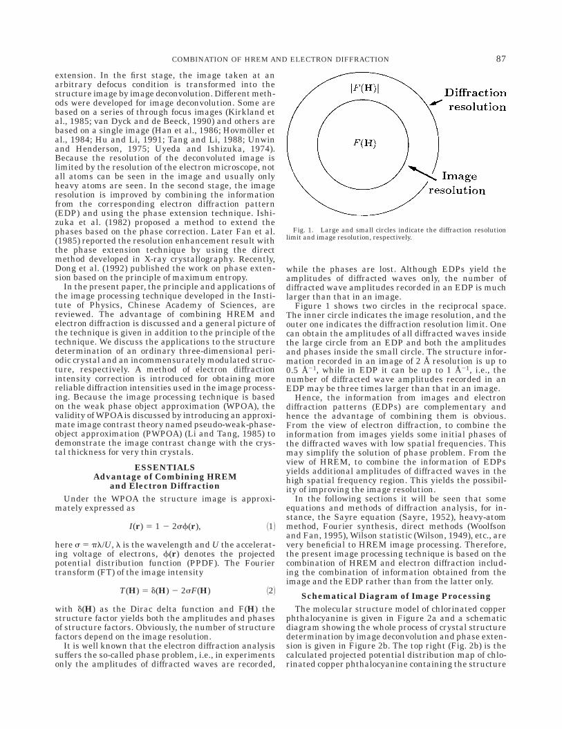
Figure 1 shows two circles in the reciprocal space.The inner circle indicates the image resolution, and theouter one indicates the diffraction resolution limit. Onecan obtain the amplitudes of all diffracted waves insidethe large circle from an EDP and both the amplitudesand phases inside the small circle. The structure infor-mation recorded in an image of 2 Å resolution is up to0.5 Å21, while in EDP it can be up to 1 Å21, i.e., thenumber of diffracted wave amplitudes recorded in anEDP may be three times larger than that in an image.
Hence, the information from images and electrondiffraction patterns (EDPs) are complementary andhence the advantage of combining them is obvious.From the view of electron diffraction, to combine theinformation from images yields some initial phases ofthe diffracted waves with low spatial frequencies. Thismay simplify the solution of phase problem. From theview of HREM, to combine the information of EDPsyields additional amplitudes of diffracted waves in thehigh spatial frequency region. This yields the possibil-ity of improving the image resolution.
In the following sections it will be seen that someequations and methods of diffraction analysis, for in-stance, the Sayre equation (Sayre, 1952), heavy-atommethod, Fourier synthesis, direct methods (Woolfsonand Fan, 1995), Wilson statistic (Wilson, 1949), etc., arevery beneficial to HREM image processing. Therefore,the present image processing technique is based on thecombination of HREM and electron diffraction includ-ing the combination of information obtained from theimage and the EDP rather than from the latter only.
Schematical Diagram of Image ProcessingThe molecular structure model of chlorinated copper
phthalocyanine is given in Figure 2a and a schematicdiagram showing the whole process of crystal structuredetermination by image deconvolution and phase exten-sion is given in Figure 2b. The top right (Fig. 2b) is thecalculated projected potential distribution map of chlo-rinated copper phthalocyanine containing the structure
Fig. 1. Large and small circles indicate the diffraction resolutionlimit and image resolution, respectively.
87COMBINATION OF HREM AND ELECTRON DIFFRACTION
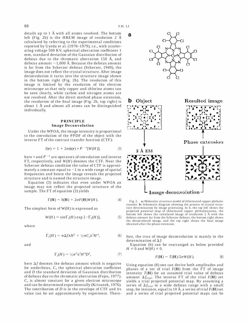
details up to 1 Å with all atoms resolved. The bottomleft (Fig. 2b) is the HREM image of resolution 2 Åcalculated by referring to the experimental conditionsreported by Uyeda et al. (1978–1979), i.e., with acceler-ating voltage 500 KV, spherical aberration coefficient 1mm, standard deviation of the Gaussian distribution ofdefocus due to the chromatic aberration 150 Å, anddefocus amount 21,000 Å. Because the defocus amountis far from the Scherzer defocus (Scherzer, 1949), theimage does not reflect the crystal structure. After imagedeconvolution it turns into the structure image shownin the bottom right (Fig. 2b). The resolution of thisimage is limited by the resolution of the electronmicroscope so that only copper and chlorine atoms canbe seen clearly, while carbon and nitrogen atoms arenot resolved. After the direct method phase extension,the resolution of the final image (Fig. 2b, top right) isabout 1 Å and almost all atoms can be distinguishedindividually.
PRINCIPLEImage Deconvolution
Under the WPOA, the image intensity is proportionalto the convolution of the PPDF of the object with theinverse FT of the contrast transfer function (CTF):
I(r) 5 1 1 2sf(r) p F 21[W(H )], 132
here p and F 21 are operators of convolution and inverseFT, respectively, and W(H) denotes the CTF. Near theScherzer defocus condition the value of CTF is approxi-mately a constant equal to 21 in a wide range of spatialfrequencies and hence the image reveals the projectedstructure and is named the structure image.
Equation (3) indicates that even under WPOA animage may not reflect the projected structure of thesample. The FT of equation (3) yields
T(H) 5 d(H) 1 2sF(H)W(H ). 142
The simplest form of W(H) is expressed as
W(H ) 5 sinG1(H ) exp [2G2(H )], 152
where
G1(H ) 5 pD flH2 1 1⁄2pCsl3H4, 162
and
G2(H ) 5 1⁄2p2l2H4D2, 172
here D f denotes the defocus amount which is negativefor underfocus, Cs the spherical aberration coefficientand D the standard deviation of Gaussian distributionof defocus due to the chromatic aberration (Fejes, 1977).Cs is almost constant for a given electron microscopeand can be determined experimentally (Krivanek, 1976).The contribution of D is in the envelope of CTF and itsvalue can be set approximately by experience. There-
fore, the crux of image deconvolution is mainly in thedetermination of D f:
Equation (6) can be rearranged as below providedH Þ 0 and W(H) Þ 0.
F(H) 5 T(H) /2sW(H ). 182
Using equation (8) one can derive both amplitudes andphases of a set of trial F(H) from the FT of imageintensity T(H) for an assumed trial value of defocusamount D ftrial. The inverse FT of the trial F(H) setyields a trial projected potential map. By assuming aseries of D ftrial in a wide defocus range with a smallstep, for instance, equal to 10 Å, a series of trial F(H) setand a series of trial projected potential maps can be
Fig. 2. a: Molecular structure model of chlorinated copper phthalo-cyanine. b: Schematic diagram showing the process of crystal struc-ture determination by image processing. In b, the top left shows theprojected potential map of chlorinated copper phthalocyanine, thebottom left shows the calculated image of resolution 2 Å with thedefocus amount far from the Scherzer defocus, the bottom right showsthe deconvoluted image, and the top right shows the final imageobtained after the phase extension.
88 F.H. LI
obtained. Thus, the problem becomes to set a criterionfor choosing the right set of F(H) from among a series oftrial F(H) sets in the reciprocal space or choosing theright projected potential map from among a series oftrial projected potential maps in the real space.
Criterion based on Sayre equation (Han et al.,1986). In X-ray crystallography the relationship amongstructure factors for a crystal is described by the Sayreequation (Sayre, 1952):
F(H) 5u
VSH8F(H8) F(H 2 H8), 192
where u 5 f (H)/g(H), f (H) denotes the atomic scatteringfactor, g(H) the scattering factor of squared atoms, andV the volume of the unit cell. Obviously, a right set ofstructure factors should obey the Sayre equation. Theextent of satisfaction of structure factors to Sayreequation can be judged by the figures of merit (Woolfsonand Fan, 1995).
Criterion based on an approximation to CTF(Tang and Li, 1988). To combine equations (5) and (8)we obtain
sinG1(H ) 5T(H)
2sF(H) exp [2G2(H )]. 1102
Forming the squared magnitude of both side of equa-tion (10) leads to
sin2G1(H ) 50T(H) 02
4 0sF(H) 02 exp2 [2G2(H )], 1112
here 4 0sF(H) 02 is the diffraction intensity. The values ofobserved sin2G1(H), noted as sin2G1(H)o can be deter-mined according to equation (11) from the observedimage and its corresponding EDP, while a series calcu-lated sin2G1(H), noted as sin2G1(H)c, can be obtainedwith a series of assigned D ftrial from equation (6). TheD f which leads to a minimum
SH 0sin2G1(H )o 2 sin2G1(H )c 0
is utilized for image deconvolution.
Criterion based on principle of maximum en-tropy (Hu and Li, 1991). When the PPDF inside theunit cell is described by sampled values correspondingto N pixels, the entropy of the PPDF is defined as(Shannon and Weaver, 1949)
S 5 2oi51
N
Pi ln Pi, 1122
and
Pi 5 fi /oi51
N
fi, 1132
where fi ; f(ri) denotes the value of projected potentialof the ith pixel. It is known that the PPDF of crystals
always corresponds to the maximum value of entropydefined by equation (12) (Collins, 1982).
The values of entropy for all trial projected potentialmap can be derived by use of equations (12) and (13).The D ftrial that corresponds to the maximum entropywould be close to the true defocus amount.
The image deconvolution can be carried out by usingonly a single image or by combining phases of structurefactors from the image and amplitudes from the corre-sponding EDP of a very thin sample. The above-mentioned different methods of image deconvolutiongive similar results that can be confirmed by oneanother.
Image Resolution EnhancementAn electron diffraction pattern usually contains ob-
servable reflections up to 1 Å21. This implies thepossibility of obtaining from the electron diffractiondata a structure image of resolution 1 Å, providedphases of structure factors can be obtained. Such aresolution is considerably higher than that reachedfrom an image. In addition, the electron diffractionintensities are independent of defocus and sphericalaberration of the objective lens. However, the problemis the loss of phases in electron diffraction experiments.Fortunately, an optimum defocus image can usuallyprovide the phase information corresponding to a reso-lution better than 2 Å, which can reduce the complexityof the solution of the phase problem. Structure factorsof low special frequencies included in the small circleshown in Figure 1 with their phases from the deconvo-luted image and amplitudes from the correspondingEDP are put in the right-hand side to calculate a newstructure factor of spatial frequency higher than before.Hence, an image with improved resolution can beobtained by such a phase extrapolation procedure usinginitial phases of structure factors from the image andamplitudes from the EDP (Fan et al., 1985, 1991a; Fu etal., 1994; Hu et al., 1992; Ishizuka et al., 1982). Thedirect method phase extension based on the Sayreequation has been proved to be very effective (Fan et al.,1991a; Fu et al., 1994; Hu et al., 1992).
STRUCTURE DETERMINATIONOF K2O · Nb2O5 (Hu et al., 1992)
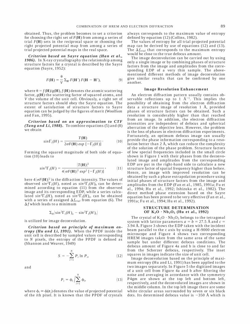
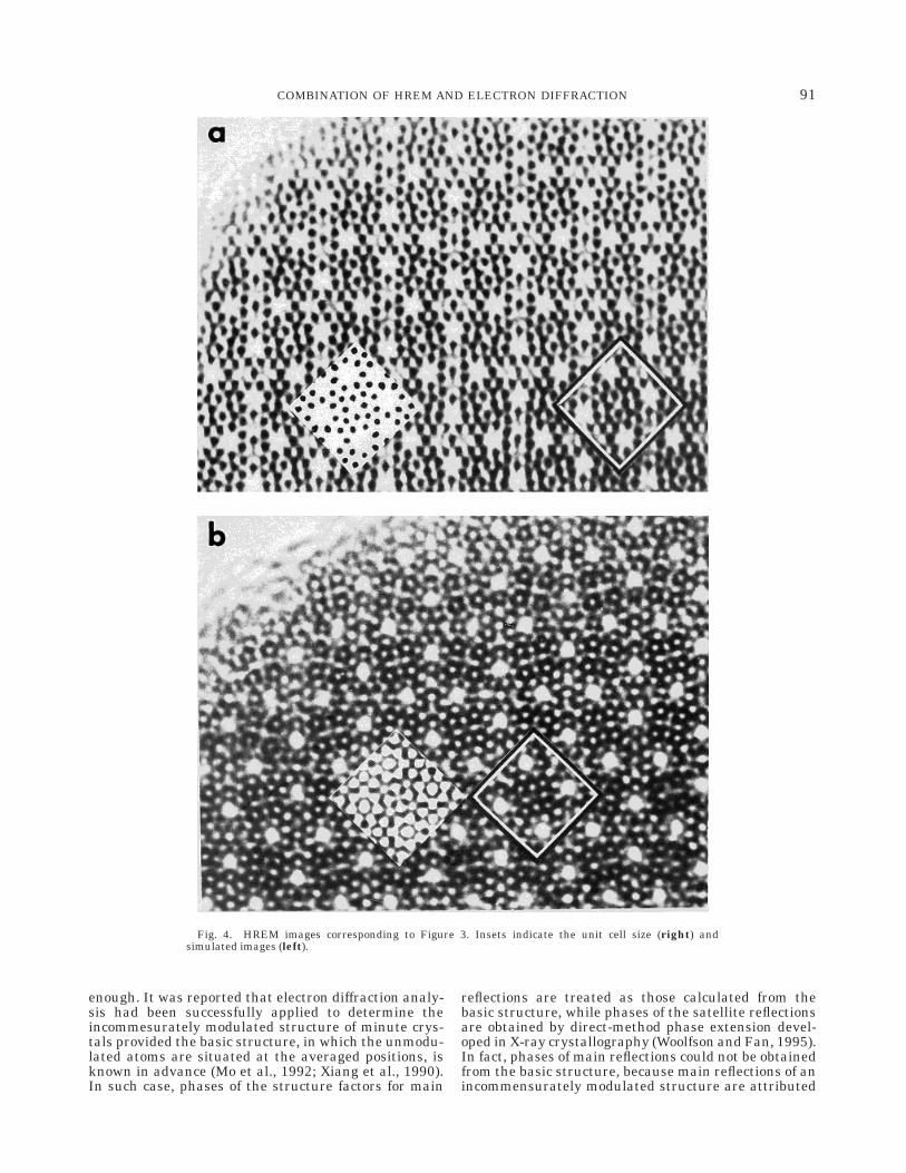
The crystal of K2O · Nb2O5 belongs to the tetragonalsystem with lattice parameters a 5 b 5 27.5 Å and c 53.94 Å. Figure 3 shows the EDP taken with the incidentbeam parallel to the c axis by using a H-9000 electronmicroscope and Figure 4 shows two correspondingHREM images taken from the same area of the samesample but under different defocus conditions. Thedefocus amount of Figure 4a and b is close to and farfrom the Scherzer defocus, respectively. The insetsquares in images indicate the size of unit cell.
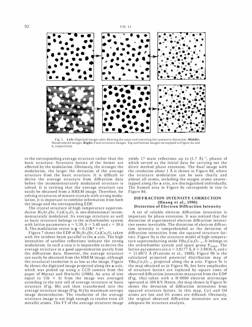
Image deconvolution based on the principle of maxi-mum entropy (Hu and Li, 1991) has been applied to thetwo images separately. In Figure 5 the digitized imagesof a unit cell from Figure 4a and b after filtering thenoise and averaging in accordance with the symmetryP4gm are shown at the top left and bottom left,respectively, and the deconvoluted images are shown inthe middle column. In the top left image there are somewhite circular areas surrounded by seven or six blackdots. Its determined defocus value is 2350 Å which is
89COMBINATION OF HREM AND ELECTRON DIFFRACTION
close to the Scherzer defocus. This is the reason that thedeconvoluted image (Fig. 5, top middle) is similar to theoriginal image (Fig. 5, top left). The difference betweenthe deconvoluted and original images is that there aremore black dots in the deconvoluted image than in theoriginal one. For instance, each white circular area isnow occupied by a small black dot. Small black dots alsoappear at the center and vertices of the unit cell. On thecontrary the deconvoluted image shown in the bottommiddle of Figure 5 is much different from the originalimage (Fig. 5, bottom left). The determined defocusamount for the bottom left image is 2850 Å, which is farfrom the Scherzer defocus so that the image contrastchanges drastically after image deconvolution. The factthat the two original images are much different fromeach other, while the two deconvoluted images aresimilar to each other indicates that the image deconvo-lution is effective in transforming the image with anarbitrary defocus value into the structure image. Byreferring to the principle of image formation, the chemi-cal formula of the crystal and the structure chemistry, itis reasonable to assume that all the darkest dots in thetwo deconvoluted images represent niobium atoms andthe weak dots that are surrounded by six or sevenniobium atoms represent potassium atoms. The dots atthe center and vertices of the unit cell are assumed to beniobium atoms but with the occupancy smaller thanunity. Because the resolution of deconvoluted imagesare limited by the resolution of the electron microscope,it cannot be expected to see all atoms in such low-resolution structure images.
The present result indicates that the image deconvo-lution may yield some important structure informationeven when the image is taken near the Scherzerdefocus. For instance, at the present case, although theimage shown in Figure 4a was taken near the Scherzerdefocus, potassium atoms cannot be seen until theimage deconvolution was carried out.
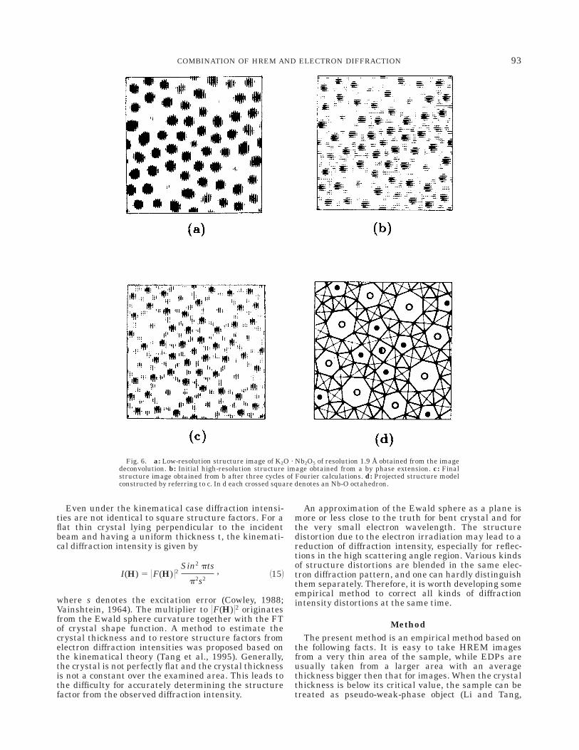
To obtain high-resolution structure images and deter-mine position of atoms, the phase extension was carried
out by using the Sayre equation (equation (9)). Struc-ture factors with the amplitudes obtained from the EDP(Fig. 3) and the phases from the deconvoluted image ofresolution 1.9 Å (Fig. 6a) were used to calculate thephases for reflections within the region between (1.9Å)21 and 1 Å21; A projected potential map (Fig. 6b) wascalculated using amplitudes of structure factors fromthe EDP and phases from the deconvoluted image (Fig.6a) as well as from the result of phase extension. It canbe seen that many additional diffuse weak black con-trast areas appear in Figure 6b. Fourier synthesis wasused to improve the obtained projected potential mapshowed in Figure 6b. For this, at first atomic coordi-nates were read from Figure 6a and structure factorswere calculated, then a new projected potential mapwas calculated by using the phases of newly calculatedstructure factors and amplitudes from the diffractionintensities. The process was carried out interactivelyuntil the result is convergent. The final high-resolutionstructure image obtained after three cycles of Fouriercalculation is shown in Figure 6c. All atoms includingoxygen atoms are resolved in the image and the imagecontrast changes monotonously with the atomic weight.
The structure model constructed from the final struc-ture image (Fig. 6c) is shown in Figure 6d. It consists ofNb-O octahedra with the oxygen atom at the center andniobium atoms at vertices. Nb-O octahedra link oneanother by sharing vertices to form channels of differ-ent types. Heptagonal and hexagonal channels areoccupied by potassium atoms, tetragonal and pentago-nal channels by niobium atoms, and triangular chan-nels are empty. The atomic occupancy inside the tetrago-nal channels was assumed to be equal to 0.5. Theresidual factors were calculated with the formula
R 5S 00Fc(H) 02 0Fo(H) 00
S 0Fc(H) 0, 1142
where 0Fo(H) 0 denotes the amplitudes of structure fac-tors obtained from the electron diffraction intensitiesand 0Fc(H) 0 the amplitudes of structure factors calcu-lated by using the atomic coordinates obtained from thefinal high-resolution structure image. Their values are0.3871, 0.3014, 0.2863, and 0.2808 for results after thephase extension and the first, second, and third Fouriercalculations, respectively. The images simulated on thebasis of the determined structure for crystal thickness39.4 Å and defocus values 2300 Å and 2830 Å areinserted on the bottom left of Figure 4a and b, respec-tively, to show the contrast agreement with experimen-tal images.
DETERMINATION OF INCOMMENSURATELYMODULATED STRUCTURE (Fu et al., 1994)It is well known that an incommensurately modu-
lated structure can be described as the section of ahigh-dimensional periodic structure with the real physi-cal space (de Wolf, 1974). In principle, methods ofcrystal structure analysis for ordinary three-dimen-sional periodic structure remain valid for incommensu-rately modulated structures. X-ray diffraction analysisis no doubt a reliable technique to determine three-dimensional as well as high-dimensional structures(Hao et al., 1987) in case the crystal size is large
Fig. 3. EDP of K2O · Nb2O5 taken with the incident beam parallelto the c axis.
90 F.H. LI
enough. It was reported that electron diffraction analy-sis had been successfully applied to determine theincommesurately modulated structure of minute crys-tals provided the basic structure, in which the unmodu-lated atoms are situated at the averaged positions, isknown in advance (Mo et al., 1992; Xiang et al., 1990).In such case, phases of the structure factors for main
reflections are treated as those calculated from thebasic structure, while phases of the satellite reflectionsare obtained by direct-method phase extension devel-oped in X-ray crystallography (Woolfson and Fan, 1995).In fact, phases of main reflections could not be obtainedfrom the basic structure, because main reflections of anincommensurately modulated structure are attributed
Fig. 4. HREM images corresponding to Figure 3. Insets indicate the unit cell size (right) andsimulated images (left).
91COMBINATION OF HREM AND ELECTRON DIFFRACTION
to the corresponding average structure rather than thebasic structure. Structure factors of the former areaffected by the modulation. Obviously, the stronger themodulation, the larger the deviation of the averagestructure from the basic structure. It is difficult toderive the average structure from diffraction databefore the incommensurately modulated structure issolved. It is exciting that the average structure caneasily be obtained from a HREM image. Therefore, forsolving structures of minute crystals with strong modu-lation, it is important to combine information from boththe image and the corresponding EDP.
The crystal structure of high temperature supercon-ductor Bi2Sr2(Sr, Ca)Cu2Ox is one-dimensional incom-mensurately modulated. Its average structure as wellas basic structure belongs to the orthorhombic systemwith lattice parameters a 5 5.39, b 5 5.40 and c 5 30.6Å. The modulation vector is q 5 0.21b* 1 c*.
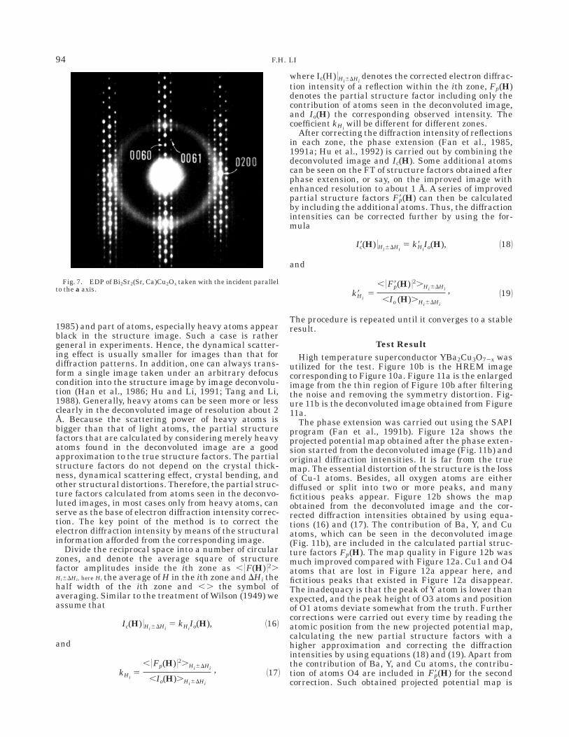
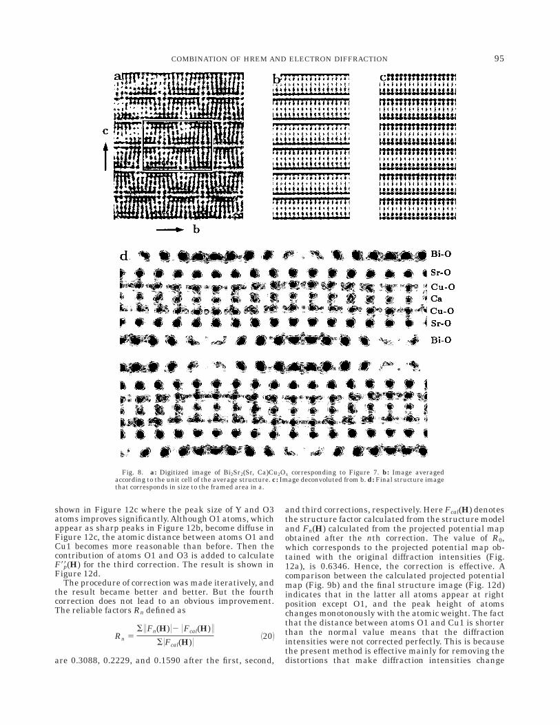
Figure 7 shows the EDP of Bi2Sr2(Sr, Ca)Cu2Ox takenwith the incident beam parallel to the a axis. The highintensities of satellite reflections indicate the strongmodulation. In such a case it is impossible to derive theaverage structure in a good approximation purely fromthe diffraction data. However, the average structurecan easily be obtained from the HREM image, althoughthe structural resolution is as low as the image. Figure8a shows the digitized image projected along the a axis,which was picked up using a CCD camera from thepaper of Matsui and Horiuchi (1988). An area of sizeequal to 15b 3 3c from the image was averagedaccording to the unit cell of average structure or basicstructure (Fig. 8b) and then transformed into theaverage structure image (Fig. 8c) by maximum entropyimage deconvolution. The resolution of the averagestructure image is not high enough to resolve even allmetallic atoms. The FT of the average structure image
yields 17 main reflections up to (1.7 Å)21, phases ofwhich served as the initial data for carrying out thedirect method phase extension. The final image withthe resolution about 1 Å is shown in Figure 8d, wherethe structure modulation can be seen clearly andalmost all atoms, including the oxygen atoms unover-lapped along the a axis, are distinguished individually.The framed area in Figure 8a corresponds in size toFigure 8d.
DIFFRACTION INTENSITY CORRECTION(Huang et al., 1996)
Distortion of Electron Diffraction IntensityA set of reliable electron diffraction intensities is
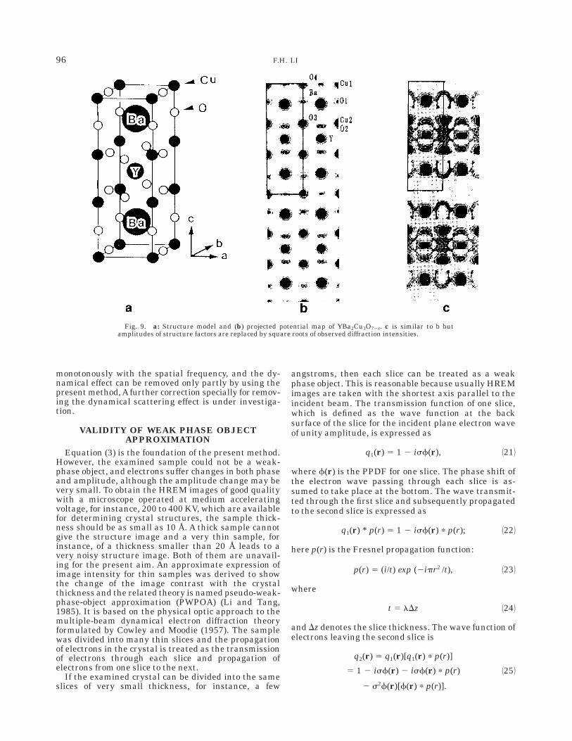
important for phase extension. It was noticed that thedistortion of experimental electron diffraction intensi-ties seems inevitable. The distortion of electron diffrac-tion intensity is comprehended as the deviation ofdiffraction intensities from the squared structure fac-tors. Figure 9a is the structure model of high tempera-ture superconducting oxide YBa2Cu3O72x. It belongs tothe orthorhombic system and space group Pmmm. Thelattice parameters are a 5 3.8177 Å, b 5 3.8836 Å, and c5 11.6872 Å (Francois et al., 1988). Figure 9b is thecalculated projected potential distribution map ofYBa2Cu3O72x projected along the a axis. Figure 9c isthe map obtained as in Figure 9b, but here amplitudesof structure factors are replaced by square roots ofobserved diffraction intensities measured from the EDP(Fig. 10a) taken with a H-9000 electron microscopeoperated at 300 KV. Hence, the map shown in Figure 9cshows the deviation of diffraction intensities fromsquared structure factors. In this map, Cu1 and O4atoms are lost and O1 atoms are diffused. Obviously,the original observed diffraction intensities are notadequate for structure analysis.
Fig. 5. Left: Digitized images after filtering the noise and removing the symmetry distortion. Middle:Deconvoluted images. Right: Final structure images. Top and bottom images correspond to Figure 4a andb, respectively.
92 F.H. LI
Even under the kinematical case diffraction intensi-ties are not identical to square structure factors. For aflat thin crystal lying perpendicular to the incidentbeam and having a uniform thickness t, the kinemati-cal diffraction intensity is given by
I(H) 5 0F(H) 02Sin2 pts
p2s2, 1152
where s denotes the excitation error (Cowley, 1988;Vainshtein, 1964). The multiplier to 0F(H) 02 originatesfrom the Ewald sphere curvature together with the FTof crystal shape function. A method to estimate thecrystal thickness and to restore structure factors fromelectron diffraction intensities was proposed based onthe kinematical theory (Tang et al., 1995). Generally,the crystal is not perfectly flat and the crystal thicknessis not a constant over the examined area. This leads tothe difficulty for accurately determining the structurefactor from the observed diffraction intensity.
An approximation of the Ewald sphere as a plane ismore or less close to the truth for bent crystal and forthe very small electron wavelength. The structuredistortion due to the electron irradiation may lead to areduction of diffraction intensity, especially for reflec-tions in the high scattering angle region. Various kindsof structure distortions are blended in the same elec-tron diffraction pattern, and one can hardly distinguishthem separately. Therefore, it is worth developing someempirical method to correct all kinds of diffractionintensity distortions at the same time.
MethodThe present method is an empirical method based on
the following facts. It is easy to take HREM imagesfrom a very thin area of the sample, while EDPs areusually taken from a larger area with an averagethickness bigger then that for images. When the crystalthickness is below its critical value, the sample can betreated as pseudo-weak-phase object (Li and Tang,
Fig. 6. a: Low-resolution structure image of K2O · Nb2O5 of resolution 1.9 Å obtained from the imagedeconvolution. b: Initial high-resolution structure image obtained from a by phase extension. c: Finalstructure image obtained from b after three cycles of Fourier calculations. d: Projected structure modelconstructed by referring to c. In d each crossed square denotes an Nb-O octahedron.
93COMBINATION OF HREM AND ELECTRON DIFFRACTION
1985) and part of atoms, especially heavy atoms appearblack in the structure image. Such a case is rathergeneral in experiments. Hence, the dynamical scatter-ing effect is usually smaller for images than that fordiffraction patterns. In addition, one can always trans-form a single image taken under an arbitrary defocuscondition into the structure image by image deconvolu-tion (Han et al., 1986; Hu and Li, 1991; Tang and Li,1988). Generally, heavy atoms can be seen more or lessclearly in the deconvoluted image of resolution about 2Å. Because the scattering power of heavy atoms isbigger than that of light atoms, the partial structurefactors that are calculated by considering merely heavyatoms found in the deconvoluted image are a goodapproximation to the true structure factors. The partialstructure factors do not depend on the crystal thick-ness, dynamical scattering effect, crystal bending, andother structural distortions. Therefore, the partial struc-ture factors calculated from atoms seen in the deconvo-luted images, in most cases only from heavy atoms, canserve as the base of electron diffraction intensity correc-tion. The key point of the method is to correct theelectron diffraction intensity by means of the structuralinformation afforded from the corresponding image.
Divide the reciprocal space into a number of circularzones, and denote the average square of structurefactor amplitudes inside the ith zone as , 0F(H) 02.Hi6DHi, here Hi the average of H in the ith zone and DHi thehalf width of the ith zone and ,. the symbol ofaveraging. Similar to the treatment of Wilson (1949) weassume that
Ic(H) 0Hi6DHi5 kHi
Io(H), 1162
and
kHi5
, 0Fp(H) 02.Hi6DHi
,Io(H).Hi6DHi
, 1172
where Ic(H) 0Hi6DHidenotes the corrected electron diffrac-
tion intensity of a reflection within the ith zone, Fp(H)denotes the partial structure factor including only thecontribution of atoms seen in the deconvoluted image,and Io(H) the corresponding observed intensity. Thecoefficient kHi
will be different for different zones.After correcting the diffraction intensity of reflections
in each zone, the phase extension (Fan et al., 1985,1991a; Hu et al., 1992) is carried out by combining thedeconvoluted image and Ic(H). Some additional atomscan be seen on the FT of structure factors obtained afterphase extension, or say, on the improved image withenhanced resolution to about 1 Å. A series of improvedpartial structure factors F8p(H) can then be calculatedby including the additional atoms. Thus, the diffractionintensities can be corrected further by using the for-mula
I8c(H) 0Hi6DHi5 k8Hi
Io(H), 1182
and
k8Hi5
, 0F8p(H) 02.Hi6DHi
,Io (H).Hi6DHi
, 1192
The procedure is repeated until it converges to a stableresult.
Test ResultHigh temperature superconductor YBa2Cu3O72x was
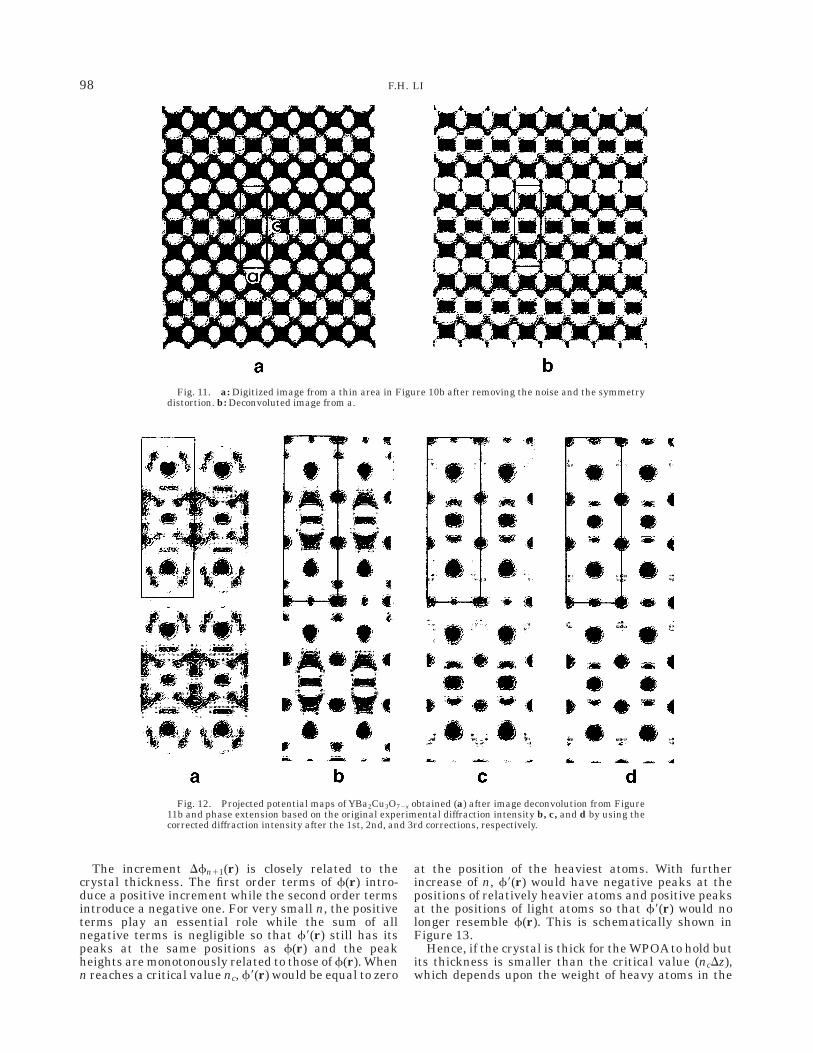
utilized for the test. Figure 10b is the HREM imagecorresponding to Figure 10a. Figure 11a is the enlargedimage from the thin region of Figure 10b after filteringthe noise and removing the symmetry distortion. Fig-ure 11b is the deconvoluted image obtained from Figure11a.
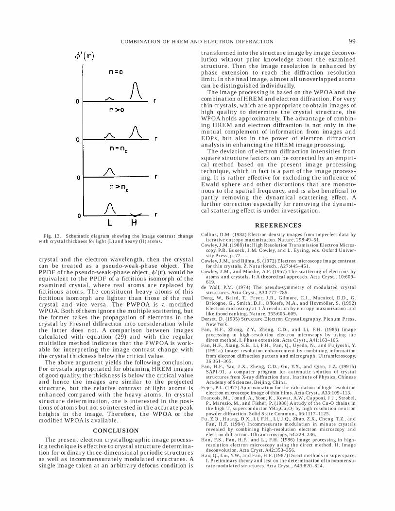
The phase extension was carried out using the SAPIprogram (Fan et al., 1991b). Figure 12a shows theprojected potential map obtained after the phase exten-sion started from the deconvoluted image (Fig. 11b) andoriginal diffraction intensities. It is far from the truemap. The essential distortion of the structure is the lossof Cu-1 atoms. Besides, all oxygen atoms are eitherdiffused or split into two or more peaks, and manyfictitious peaks appear. Figure 12b shows the mapobtained from the deconvoluted image and the cor-rected diffraction intensities obtained by using equa-tions (16) and (17). The contribution of Ba, Y, and Cuatoms, which can be seen in the deconvoluted image(Fig. 11b), are included in the calculated partial struc-ture factors Fp(H). The map quality in Figure 12b wasmuch improved compared with Figure 12a. Cu1 and O4atoms that are lost in Figure 12a appear here, andfictitious peaks that existed in Figure 12a disappear.The inadequacy is that the peak of Y atom is lower thanexpected, and the peak height of O3 atoms and positionof O1 atoms deviate somewhat from the truth. Furthercorrections were carried out every time by reading theatomic position from the new projected potential map,calculating the new partial structure factors with ahigher approximation and correcting the diffractionintensities by using equations (18) and (19). Apart fromthe contribution of Ba, Y, and Cu atoms, the contribu-tion of atoms O4 are included in F8p(H) for the secondcorrection. Such obtained projected potential map is
Fig. 7. EDP of Bi2Sr2(Sr, Ca)Cu2Ox taken with the incident parallelto the a axis.
94 F.H. LI
shown in Figure 12c where the peak size of Y and O3atoms improves significantly.Although O1 atoms, whichappear as sharp peaks in Figure 12b, become diffuse inFigure 12c, the atomic distance between atoms O1 andCu1 becomes more reasonable than before. Then thecontribution of atoms O1 and O3 is added to calculateF88p(H) for the third correction. The result is shown inFigure 12d.
The procedure of correction was made iteratively, andthe result became better and better. But the fourthcorrection does not lead to an obvious improvement.The reliable factors Rn defined as
Rn 5S 00Fn(H) 02 0Fcal(H) 00
S 0Fcal(H) 01202
are 0.3088, 0.2229, and 0.1590 after the first, second,
and third corrections, respectively. Here Fcal(H) denotesthe structure factor calculated from the structure modeland Fn(H) calculated from the projected potential mapobtained after the nth correction. The value of R0,which corresponds to the projected potential map ob-tained with the original diffraction intensities (Fig.12a), is 0.6346. Hence, the correction is effective. Acomparison between the calculated projected potentialmap (Fig. 9b) and the final structure image (Fig. 12d)indicates that in the latter all atoms appear at rightposition except O1, and the peak height of atomschanges monotonously with the atomic weight. The factthat the distance between atoms O1 and Cu1 is shorterthan the normal value means that the diffractionintensities were not corrected perfectly. This is becausethe present method is effective mainly for removing thedistortions that make diffraction intensities change
Fig. 8. a: Digitized image of Bi2Sr2(Sr, Ca)Cu2Ox corresponding to Figure 7. b: Image averagedaccording to the unit cell of the average structure. c: Image deconvoluted from b. d: Final structure imagethat corresponds in size to the framed area in a.
95COMBINATION OF HREM AND ELECTRON DIFFRACTION
monotonously with the spatial frequency, and the dy-namical effect can be removed only partly by using thepresent method,Afurther correction specially for remov-ing the dynamical scattering effect is under investiga-tion.
VALIDITY OF WEAK PHASE OBJECTAPPROXIMATION
Equation (3) is the foundation of the present method.However, the examined sample could not be a weak-phase object, and electrons suffer changes in both phaseand amplitude, although the amplitude change may bevery small. To obtain the HREM images of good qualitywith a microscope operated at medium acceleratingvoltage, for instance, 200 to 400 KV, which are availablefor determining crystal structures, the sample thick-ness should be as small as 10 Å. A thick sample cannotgive the structure image and a very thin sample, forinstance, of a thickness smaller than 20 Å leads to avery noisy structure image. Both of them are unavail-ing for the present aim. An approximate expression ofimage intensity for thin samples was derived to showthe change of the image contrast with the crystalthickness and the related theory is named pseudo-weak-phase-object approximation (PWPOA) (Li and Tang,1985). It is based on the physical optic approach to themultiple-beam dynamical electron diffraction theoryformulated by Cowley and Moodie (1957). The samplewas divided into many thin slices and the propagationof electrons in the crystal is treated as the transmissionof electrons through each slice and propagation ofelectrons from one slice to the next.
If the examined crystal can be divided into the sameslices of very small thickness, for instance, a few
angstroms, then each slice can be treated as a weakphase object. This is reasonable because usually HREMimages are taken with the shortest axis parallel to theincident beam. The transmission function of one slice,which is defined as the wave function at the backsurface of the slice for the incident plane electron waveof unity amplitude, is expressed as
q1(r) 5 1 2 isf(r), 1212
where f(r) is the PPDF for one slice. The phase shift ofthe electron wave passing through each slice is as-sumed to take place at the bottom. The wave transmit-ted through the first slice and subsequently propagatedto the second slice is expressed as
q1(r) * p(r) 5 1 2 isf(r) p p(r); 1222
here p(r) is the Fresnel propagation function:
p(r) 5 (i/t) exp (2ipr2 /t), 1232
where
t 5 lDz 1242
and Dz denotes the slice thickness. The wave function ofelectrons leaving the second slice is
q2(r) 5 q1(r)[q1(r) p p(r)]
5 1 2 isf(r) 2 isf(r) p p(r) 1252
2 s2f(r)[f(r) p p(r)].
Fig. 9. a: Structure model and (b) projected potential map of YBa2Cu3O72x. c is similar to b butamplitudes of structure factors are replaced by square roots of observed diffraction intensities.
96 F.H. LI

The last term on the right-hand side of equation (25)indicates the double scattering, which can be ignoredcompared with the first-order term of f(r) for very thinslices. Hence,
q2(r) 5 1 2 isf(r) 2 isf(r) p p(r). 1262
Obviously, q2(r) is the transmission function of thecrystal consisting of two slices.
Let qn11 represent the transmission function consist-ing of n 1 1 slices, then
qn11 5 q1(r)n [···2[q1(r)1[q1(r)
p p(r)]1p p(r)]2 ··· p p(r)]n.(27)
If the multiple scattering is ignored in each slice, qn11can be simplified as
Under the Scherzer defocus condition the imageintensity for the crystal consisting of n 1 1 slices is
In11(r) 5 1 2 2sf(r) 1 s2f2(r)
2 2sf(r) p oj51
n
Sj(r)
1 2s2f(r) 3f(r) p oj51
n
Sj(r)41 s2 1f(r) p o
j51
n
Sj(r)22
1 s2 1f(r) p oj51
n
Cj(r)22
,
(29)
where
Sj(r) 5 (1/jt) sin (pr2/jt), 1302
Cj(r) 5 (1/jt) cos (pr2/jt). 1312
The first two terms of equation (29) represent the imageintensity for the one-slice crystal, or rather the imageintensity in WPOA. s2f2(r) can be ignored, comparedwith 2sf(r), while other additional terms in (29) aresignificant because they are dependent upon the crystalthickness and modify the image contrast appreciablywith an increase in thickness.
Equation (29) can be rearranged into
In11(r) 5 1 2 2sf8(r), 1322
where
f8(r) 5 f(r) 1 Dfn11(r) 1332
and
Dfn11(r) 5 f(r) p oj51
n
Sj(r)
2 sf(r) 3f(r) p oj51
n
Sj(r)42
s
2 1f(r) p oj51
n
Sj(r)22
2s
2 1f(r) p oj51
n
Cj(r)22.
(34)
Fig. 10. a Electron diffraction pattern and (b) HREM image ofYBa2Cu3O72x taken with the incident beam parallel to the a axis
qn11 5 1 2 isf(r) 2 isf(r) p p(r) 2 isf(r) p p(r)
p p(r) ··· 2 isf(r) p p(r) p p(r) p···p p(r).
pn times
(28)5
97COMBINATION OF HREM AND ELECTRON DIFFRACTION
The increment Dfn11(r) is closely related to thecrystal thickness. The first order terms of f(r) intro-duce a positive increment while the second order termsintroduce a negative one. For very small n, the positiveterms play an essential role while the sum of allnegative terms is negligible so that f8(r) still has itspeaks at the same positions as f(r) and the peakheights are monotonously related to those of f(r). Whenn reaches a critical value nc, f8(r) would be equal to zero
at the position of the heaviest atoms. With furtherincrease of n, f8(r) would have negative peaks at thepositions of relatively heavier atoms and positive peaksat the positions of light atoms so that f8(r) would nolonger resemble f(r). This is schematically shown inFigure 13.
Hence, if the crystal is thick for the WPOA to hold butits thickness is smaller than the critical value (ncDz),which depends upon the weight of heavy atoms in the
Fig. 11. a: Digitized image from a thin area in Figure 10b after removing the noise and the symmetrydistortion. b: Deconvoluted image from a.
Fig. 12. Projected potential maps of YBa2Cu3O72x obtained (a) after image deconvolution from Figure11b and phase extension based on the original experimental diffraction intensity b, c, and d by using thecorrected diffraction intensity after the 1st, 2nd, and 3rd corrections, respectively.
98 F.H. LI
crystal and the electron wavelength, then the crystalcan be treated as a pseudo-weak-phase object. ThePPDF of the pseudo-weak-phase object, f8(r), would beequivalent to the PPDF of a fictitious isomorph of theexamined crystal, where real atoms are replaced byfictitious atoms. The constituent heavy atoms of thisfictitious isomorph are lighter than those of the realcrystal and vice versa. The PWPOA is a modifiedWPOA. Both of them ignore the multiple scattering, butthe former takes the propagation of electrons in thecrystal by Fresnel diffraction into consideration whilethe latter does not. A comparison between imagescalculated with equation (29) and with the regularmultislice method indicates that the PWPOA is work-able for interpreting the image contrast change withthe crystal thickness below the critical value.
The above argument yields the following conclusion.For crystals appropriated for obtaining HREM imagesof good quality, the thickness is below the critical valueand hence the images are similar to the projectedstructure, but the relative contrast of light atoms isenhanced compared with the heavy atoms. In crystalstructure determination, one is interested in the posi-tions of atoms but not so interested in the accurate peakheights in the image. Therefore, the WPOA or themodified WPOA is available.
CONCLUSIONThe present electron crystallographic image process-
ing technique is effective to crystal structure determina-tion for ordinary three-dimensional periodic structuresas well as incommensurately modulated structures. Asingle image taken at an arbitrary defocus condition is
transformed into the structure image by image deconvo-lution without prior knowledge about the examinedstructure. Then the image resolution is enhanced byphase extension to reach the diffraction resolutionlimit. In the final image, almost all unoverlapped atomscan be distinguished individually.
The image processing is based on the WPOA and thecombination of HREM and electron diffraction. For verythin crystals, which are appropriate to obtain images ofhigh quality to determine the crystal structure, theWPOA holds approximately. The advantage of combin-ing HREM and electron diffraction is not only in themutual complement of information from images andEDPs, but also in the power of electron diffractionanalysis in enhancing the HREM image processing.
The deviation of electron diffraction intensities fromsquare structure factors can be corrected by an empiri-cal method based on the present image processingtechnique, which in fact is a part of the image process-ing. It is rather effective for excluding the influence ofEwald sphere and other distortions that are monoto-nous to the spatial frequency, and is also beneficial topartly removing the dynamical scattering effect. Afurther correction especially for removing the dynami-cal scattering effect is under investigation.
REFERENCESCollins, D.M. (1982) Electron density images from imperfect data by
iterative entropy maximization. Nature, 298:49–51.Cowley, J.M. (1988) In: High Resolution Transmission Electron Micros-
copy. P.R. Buseck, J.M. Cowley, and L. Eyring, eds. Oxford Univer-sity Press, p. 72.
Cowley, J.M., and Iijima, S. (1972) Electron microscope image contrastfor thin crystals. Z. Naturforsch., A27:445–451.
Cowley, J.M., and Moodie, A.F. (1957) The scattering of electrons byatoms and crystals. I: A theoretical approach. Acta Cryst., 10:609–619.
de Wolf, P.M. (1974) The pseudo-symmetry of modulated crystalstructures. Acta Cryst., A30:777–785.
Dong, W., Baird, T., Fryer, J.R., Gilmore, C.J., Macnicol, D.D., G.Bricogne, G., Smith, D.J., O’Keefe, M.A., and Hovmoller, S. (1992)Electron microscopy at 1 Å resolution by entropy maximization andlikelihood ranking. Nature, 355:605–609.
Dorset, D. (1995) Structure Electron Crystallography. Plenum Press,New York.
Fan, H.F., Zhong, Z.Y., Zheng, C.D., and Li, F.H. (1985) Imageprocessing in high-resolution electron microscopy by using thedirect method. I. Phase extension. Acta Cryst., A41:163–165.
Fan, H.F., Xiang, S.B., Li, F.H., Pan, Q., Uyeda, N., and Fujiyoshi, Y.(1991a) Image resolution enhancement by combining informationfrom electron diffraction pattern and micrograph. Ultramicroscopy,36:361–365.
Fan, H.F., Yao, J.X., Zheng, C.D., Gu, Y.X., and Qian, J.Z. (1991b)SAPI-91, a computer program for automatic solution of crystalstructures from X-ray diffraction data. Institute of Physics, ChineseAcademy of Sciences, Beijing, China.
Fejes, P.L. (1977) Approximation for the calculation of high-resolutionelectron microscope image of thin films. Acta Cryst., A33:109–113.
Francois, M., Jonud, A., Yoon, K., Kewat, A.W., Capponi, J.J., Strobel,P., Marezio, M., and Fisher, P. (1988) A study of the Cu-O chains inthe high Tc superconductor YBa2Cu3O7 by high resolution neutronpowder diffraction. Solid State Commun., 66:1117–1125.
Fu, Z.Q., Huang, D.X., Li, F.H., Li, J.Q., Zhao, Z.X., Cheng, T.Z., andFan, H.F. (1994) Incommesurate modulation in minute crystalsrevealed by combining high-resolution electron microscopy andelectron diffraction. Ultramicroscopy, 54:229–236.
Han, F.S., Fan, H.F., and Li, F.H. (1986) Image processing in high-resolution electron microscopy using the direct method. II. Imagedeconvolution. Acta Cryst. A42:353–356.
Hao, Q., Liu, Y.W., and Fan, H.F. (1987) Direct methods in superspace.I. Preliminary theory and test on the determination of incommensu-rate modulated structures. Acta Cryst., A43:820–824.
Fig. 13. Schematic diagram showing the image contrast changewith crystal thickness for light (L) and heavy (H) atoms.
99COMBINATION OF HREM AND ELECTRON DIFFRACTION
Hovmoller, S., Sjogren, A., Farrants, G., Sundberg, M., and Marinder,B-O. (1984) Accurate atomic positions from electron microscopy.Nature, 311:238–241.
Hu, J.J., and Li, F.H. (1991) Maximum entropy image deconvolution inhigh resolution electron microscopy. Ultramicroscopy, 35:339–350.
Hu, J.J., Li, F.H., and Fan, H.F. (1992) Crystal structure determina-tion of K2O · Nb2O5 by combining high-resolution electron micros-copy and electron diffraction. Ultramicroscopy, 41:387–397.
Huang, D.X., Liu, W., Gu, Y.X., Xiong, J.W., Fan, H.F., and Li, F.H.(1996) A method of electron diffraction intensity correction. ActaCryst. A52:152–157.
Ishizuka, K., Miyazaki, M., and Uyeda, N. (1982) Improvement ofelectron microscope images by the direct phasing method. ActaCryst., A38:408–413.
Kirkland, E.J., Siegel, B.M., Uyeda, N., and Fujiyoshi, Y. (1985) Imageprocessing of bright field electron micrographs. II. Experiments.Ultramicroscopy, 17:87–104.
Krivanek, O.L. (1976) A method for determining the coefficient ofspherical aberration from a single electron micrograph. Optik,45:97–101.
Li, F.H., and Tang, D. (1985) Pseudo-weak-phase-object approximation inhigh-resolution electron microscopy.Acta Cryst.,A41:376–382.
Matsui, Y., and Horiuchi, S. (1988) Geometrical relationships ofvarious modulated structures in Bi-Sr-Ca-Cu-O superconductorsand related compounds. Jpn. J. Appl. Phys., 27:L2306–2309.
Mo, Y.D., Cheng, T.Z., Fan, H.F., Li, J.Q., Sha, B.D., Zheng, C.D., Li,F.H., and Zhao, Z.X. (1992) Incommensurate modulation of theBi-2223 superconducting phase observed by direct-method electrondiffraction analysis. Phys. Scr., T 42:18–19.
Sayre, D. (1952) The squaring method: A new method for phasedetermination. Acta Cryst., 5:60–65.
Scherzer, O. (1949) The theoretical resolution limit of electron micro-scope. J. Appl. Phys., 20:20–29.
Shannon, C.E., and Weaver, W. (1949) The Mathematical Theory ofCommunication. University Illinois Press, Illinois.
Tang, D., and Li, F.H. (1988) A method of image restoration forpseudo-weak-phase-objects. Ultramicroscopy, 25:61–68.
Tang, D., Jannsen, J., and Zandbergen, H.W. (1995) The estimation ofcrystal thickness and the restoration of structure factor modulusfrom electron diffraction: A kinematical approach. Acta Cryst.,A51:188–197.
Unwin, P.N.T., and Henderson, R. (1975) Molecular structure determi-nation by electron microscopy of unstained crystallined specimens.J. Mol. Biol., 94:425–440.
Uyeda, N., and Ishizuka, K. (1974) Correct molecular image seeking inthe arbitrary defocus series. Proc. XIIIth Int. Cong. Electron Mi-crosc., 1:322–323.
Uyeda, N., Kobayashi, T., Suito, E., Harada, Y., and Watanabe, M.(1972) Molecular image resolution in electron microscopy. J. Appl.Phys., 43:5181–5189.
Uyeda, N., Kobayashi, T., Ishizuka, K., and Fujiyoshi, Y. (1978–1979)High voltage electron microscopy for image discrimination ofconstituent atoms in crystals and molecules. Chem. Scripta, 14:47–61.
Vainshtein, B.K. (1964) Structure Analysis by Electron Diffraction.Pergamon Press, Oxford.
van Dyck, D., and de Beeck, M. Op (1990) New direct methods forphase and structure retrieval in HREM. In: Proc. XIIth Int. Cong.Electron Microsc., 1:26–27.
Wilson, A.J.C. (1949) The probability distribution of X-ray intensities.Acta Cryst. 2:318–321.
Woolfson, M.M., and Fan, H.F. (1995) Physical and Non-PhysicalMethods of Solving Crystal Structures. Cambridge University Press,Cambridge.
Xiang, S.B., Fan, H.F., Wu, X.J., Li, F.H., and Pan, Q. (1990) Directmethods in superspace. II. The first application to an unknownincommensurate modulated structure. Acta Cryst., A:929–934.
Zvyagin, B.B. (1967) Electron Diffraction Analysis of Clay MineralStructures. Plenum Press, New York.
100 F.H. LI


![Electron Microscopy - Wikis09-10]_DOWNLOAD/4 tem ii.… · Electron Microscopy 4. TEM Basics: interactions, basic modes, sample preparation, Diffraction: elastic scattering theory,](https://img.pdfslide.us/doc/110x75/5f08e5537e708231d4243ed5/electron-microscopy-wikis-09-10download4-tem-ii-electron-microscopy-4-tem.jpg)


![Ultrafast transmission electron microscopy using a laser ...transmission electron microscopy [4], scanning electron microscopy [5], x-ray diffraction [6], scanning tunneling and atomic](https://img.pdfslide.us/doc/110x75/607eb1335ce8082131294459/ultrafast-transmission-electron-microscopy-using-a-laser-transmission-electron.jpg)