Embed Size (px)
Citation preview
Igloo
Development Kit User’s Guide
Version 1.3
Igloo Development Kit User’s Guide 1
Introduction
Thank you for purchasing the Actel IglooTM Development Kit.
This guide provides the information required to easily design low power systems using Igloo devices.
IGLOO FPGA
with example processor subsystem
1Mbyte SRAM
16Mbyte Flash
USB / Serial Connector
USB Connector (Flash Pro3
Programmer)
LEDs
Switches
AGL Development Board
LVDS Connector
Flash*Freeze Switch
2 Igloo Development Kit User’s Guide
Table of Contents Table of Contents 1 Table of Contents 2 Document Contents 4 Document Assumptions 4
Contents and System Requirements 5 Igloo Development Kit Contents 5 System Requirements 5
Hardware Components 6 Igloo Development Kit 6
Ideal Uses for the development kit 6 Applications 7 Detailed Board Description and Usage 7 Block Diagram 8 Power 8 USB Serial Interface 10 Measuring Current 11 Other Features 11 Programming or Re-Programming the Pre-Loaded Design 11 AGL Development Board Jumper Descriptions 12
Setup and Self Test 14 Software Installation 14
Installing Libero IDE v8.x 14 Installing Development Kit using the “Install CD v1.0”. 14
Testing the AGL Development Board 15 Using the SwifTraxTM Monitor 18
Description of the Pre-loaded Design 20 PiP-EC02 System Overview 20
Pre-integrated IP Embedded Controller with AMBA Bus System 20 Sample Design Tutorial 22
Functional Description 22 Hardware Implementation 22 Low Power Modes 22 Sample Design 25 Sample System Hardware Overview 26 Libero Project 26
Top Level Design 27 Constraints Files 28 Device Options 28
Program the FPGA on the AGL Development Board 28 Running the Sample Design 30
Active 30 Static - Idle 30 Static – Flash*Freeze Type 1 30 Static – Flash*Freeze Type 2 30
FG484 & FG256 Packages for the AGL FPGAs 31 484-Pin FBGA (Bottom View) 32 256-Pin FBGA (Bottom View) 33
Board Schematics 39 Product Support 40
Technical Support 40 Email 40

Igloo Development Kit User’s Guide 3
Phone 40

4 Igloo Development Kit User’s Guide
Document Contents Chapter 1 – Contents and System Requirements
describes the contents of the Igloo TM Development Kit.
Chapter 2 – Hardware Components
describes the components of the Igloo TM Development Board.
Chapter 3 – Setup and Self Test
describes how to set up the AGL Development Board and how to perform a self test. Also describes how to set up and use the SwifTraxTM Monitor.
Chapter 4 – Description of Pre-loaded Design
describes the preloaded design on the Igloo Development Board.
Chapter 5 – Sample Design Tutorial
gives a tutorial on using the included demo design.
Appendix A – FG256 and FG484 Package Connections for AGL FPGAs
provides a table listing the board connections.
Appendix B – Board Schematics
provides illustrations of the Igloo Development Board.
Appendix C – Product Support
describes Actel support services.
Document Assumptions This user’s guide assumes the following:
• You intend to use Actel Libero® Integrated Design Environment (IDE) software.
• You have installed and are familiar with:
• Actel Libero IDE v8.0 or later software.
• You are familiar with PCs and the Windows® operating system.
1
Igloo Development Kit User’s Guide 5
Contents and System Requirements
This chapter details the contents of the Igloo Development Kit and lists the power supply and software system requirements.
Igloo Development Kit Contents The Igloo Development Kit includes the following:
• AGL Development Board
• Libero IDE v8.x DVD (in DVD case)
• Igloo Development Kit Install CD with sample design
• 2 USB A to Mini-B Cables
• 4 Self-Adhesive Rubber Pads
• Quick Start Guide
System Requirements The Igloo Development Kit requires the following:
• PC or Laptop running Windows XP or Windows 2000
• 2 USB ports (connectors) on the PC or Laptop
2
Igloo Development Kit User’s Guide 6
Hardware Components
This chapter describes the hardware components of the Igloo Development Kit.
Igloo Development Kit The Igloo Development Kit consists of the following:
• 2 USB cables
• AGL Development Board
• Actel AGL600 Igloo
• 1 MByte SRAM
• 16 MByte Flash
• USB–RS232 converter chip
• GPIO connectors
• LVDS Support
• Ultra Low Power with Flash*Freeze technology
• On-board FlashPro3 circuitry
• Socketed Crystal Oscillator
• Pushbutton power-on reset circuit
• 10 test LEDs
• 10 test switches
• Expansion connectors
• 4 Self-Adhesive Rubber Pads
For further information, refer to the following appendices:
Appendix A – “Package Connections”
Appendix B – “Board Schematics”
Ideal Uses for the development kit Ideal uses for the Igloo Development Kit are the following:
• development and verification of low power systems or subsystems
• product development platform
• algorithm development
Hardware Components
Igloo Development Kit User’s Guide 7
Applications The Igloo Development Kit is ideal for use in the following applications:
• Smartphones, GPS, DCAM, PDA
• Portable industrial & medical equipment
• PC laptops, PCMCIA
• Any ultra-low power devices
Detailed Board Description and Usage The Igloo Development Kit has various advanced features that are covered in later sections of this chapter. The architecture provides access to a one-chip FPGA solution ideal for low-power systems.
Note that the Actel FPGA is soldered directly to the board. The development board is available only in a directly soldered configuration. A socketed configuration is not available.
Full schematics are available on the Install CD supplied with the development kit. See Appendix B for AGL Development Board schematics contents.
Hardware Components
8 Igloo Development Kit User’s Guide
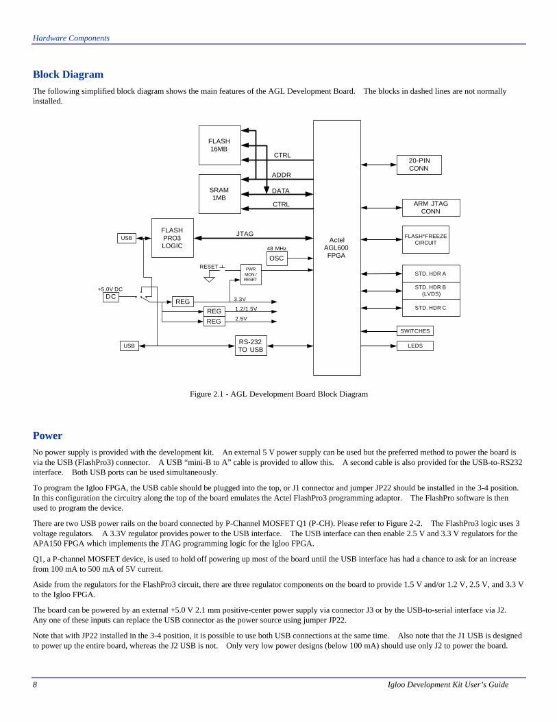
Block Diagram The following simplified block diagram shows the main features of the AGL Development Board. The blocks in dashed lines are not normally installed.
SRAM1MB
DC
ActelAGL600FPGA
PWRMON./RESET
RESET
FLASH16MB
OSC
48 MHz
+5.0V DC
20-PINCONN
3.3V
2.5V
1.2/1.5V
REG
REGREG
ADDR
DATA
CTRL
SWITCHES
LEDSRS-232TO USB
CTRL
USB
USBFLASHPRO3LOGIC
JTAG
STD. HDR C
ARM JTAGCONN
STD. HDR B(LVDS)
STD. HDR A
FLASH*FREEZECIRCUIT
Figure 2.1 - AGL Development Board Block Diagram
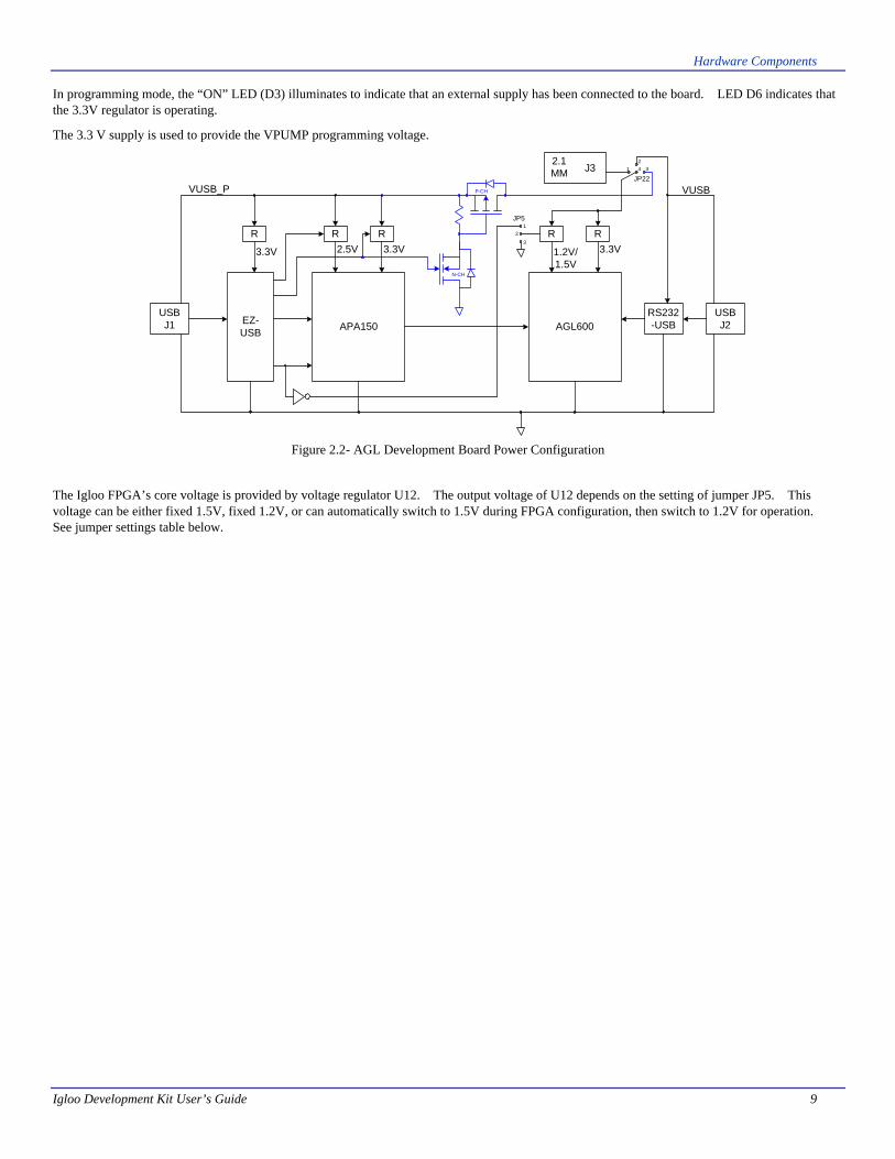
Power No power supply is provided with the development kit. An external 5 V power supply can be used but the preferred method to power the board is via the USB (FlashPro3) connector. A USB “mini-B to A” cable is provided to allow this. A second cable is also provided for the USB-to-RS232 interface. Both USB ports can be used simultaneously.
To program the Igloo FPGA, the USB cable should be plugged into the top, or J1 connector and jumper JP22 should be installed in the 3-4 position. In this configuration the circuitry along the top of the board emulates the Actel FlashPro3 programming adaptor. The FlashPro software is then used to program the device.
There are two USB power rails on the board connected by P-Channel MOSFET Q1 (P-CH). Please refer to Figure 2-2. The FlashPro3 logic uses 3 voltage regulators. A 3.3V regulator provides power to the USB interface. The USB interface can then enable 2.5 V and 3.3 V regulators for the APA150 FPGA which implements the JTAG programming logic for the Igloo FPGA.
Q1, a P-channel MOSFET device, is used to hold off powering up most of the board until the USB interface has had a chance to ask for an increase from 100 mA to 500 mA of 5V current.
Aside from the regulators for the FlashPro3 circuit, there are three regulator components on the board to provide 1.5 V and/or 1.2 V, 2.5 V, and 3.3 V to the Igloo FPGA.
The board can be powered by an external +5.0 V 2.1 mm positive-center power supply via connector J3 or by the USB-to-serial interface via J2. Any one of these inputs can replace the USB connector as the power source using jumper JP22.
Note that with JP22 installed in the 3-4 position, it is possible to use both USB connections at the same time. Also note that the J1 USB is designed to power up the entire board, whereas the J2 USB is not. Only very low power designs (below 100 mA) should use only J2 to power the board.
Hardware Components
Igloo Development Kit User’s Guide 9
In programming mode, the “ON” LED (D3) illuminates to indicate that an external supply has been connected to the board. LED D6 indicates that the 3.3V regulator is operating.
The 3.3 V supply is used to provide the VPUMP programming voltage.
USBJ1 EZ-
USBAPA150 AGL600
R R R
3.3V 3.3V2.5VR R
3.3V1.2V/1.5V
VUSB_P VUSB
USBJ2
RS232-USB
J32.1MM
N-CH
P-CH
JP2231
2
4
JP51
2
3
Figure 2.2- AGL Development Board Power Configuration
The Igloo FPGA’s core voltage is provided by voltage regulator U12. The output voltage of U12 depends on the setting of jumper JP5. This voltage can be either fixed 1.5V, fixed 1.2V, or can automatically switch to 1.5V during FPGA configuration, then switch to 1.2V for operation. See jumper settings table below.
Hardware Components
10 Igloo Development Kit User’s Guide
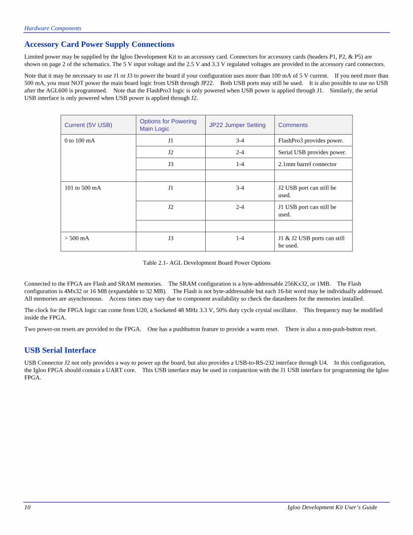
Accessory Card Power Supply Connections Limited power may be supplied by the Igloo Development Kit to an accessory card. Connectors for accessory cards (headers P1, P2, & P5) are shown on page 2 of the schematics. The 5 V input voltage and the 2.5 V and 3.3 V regulated voltages are provided to the accessory card connectors.
Note that it may be necessary to use J1 or J3 to power the board if your configuration uses more than 100 mA of 5 V current. If you need more than 500 mA, you must NOT power the main board logic from USB through JP22. Both USB ports may still be used. It is also possible to use no USB after the AGL600 is programmed. Note that the FlashPro3 logic is only powered when USB power is applied through J1. Similarly, the serial USB interface is only powered when USB power is applied through J2.
Current (5V USB) Options for Powering Main Logic
JP22 Jumper Setting Comments
J1 3-4 FlashPro3 provides power.
J2 2-4 Serial USB provides power.
J3 1-4 2.1mm barrel connector
0 to 100 mA
J1 3-4 J2 USB port can still be used.
J2 2-4 J1 USB port can still be used.
101 to 500 mA
> 500 mA J3 1-4 J1 & J2 USB ports can still be used.
Table 2.1- AGL Development Board Power Options
Connected to the FPGA are Flash and SRAM memories. The SRAM configuration is a byte-addressable 256Kx32, or 1MB. The Flash configuration is 4Mx32 or 16 MB (expandable to 32 MB). The Flash is not byte-addressable but each 16-bit word may be individually addressed. All memories are asynchronous. Access times may vary due to component availability so check the datasheets for the memories installed.
The clock for the FPGA logic can come from U20, a Socketed 48 MHz 3.3 V, 50% duty cycle crystal oscillator. This frequency may be modified inside the FPGA.
Two power-on resets are provided to the FPGA. One has a pushbutton feature to provide a warm reset. There is also a non-push-button reset.
USB Serial Interface USB Connector J2 not only provides a way to power up the board, but also provides a USB-to-RS-232 interface through U4. In this configuration, the Igloo FPGA should contain a UART core. This USB interface may be used in conjunction with the J1 USB interface for programming the Igloo FPGA.
Hardware Components
Igloo Development Kit User’s Guide 11
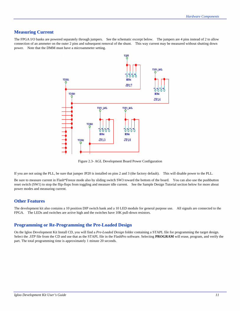
Measuring Current The FPGA I/O banks are powered separately through jumpers. See the schematic excerpt below. The jumpers are 4 pins instead of 2 to allow connection of an ammeter on the outer 2 pins and subsequent removal of the shunt. This way current may be measured without shutting down power. Note that the DMM must have a microammeter setting.
Figure 2.3- AGL Development Board Power Configuration
If you are not using the PLL, be sure that jumper JP20 is installed on pins 2 and 3 (the factory default). This will disable power to the PLL.
Be sure to measure current in Flash*Freeze mode also by sliding switch SW3 toward the bottom of the board. You can also use the pushbutton reset switch (SW1) to stop the flip-flops from toggling and measure idle current. See the Sample Design Tutorial section below for more about power modes and measuring current.
Other Features The development kit also contains a 10 position DIP switch bank and a 10 LED module for general purpose use. All signals are connected to the FPGA. The LEDs and switches are active high and the switches have 10K pull-down resistors.
Programming or Re-Programming the Pre-Loaded Design On the Igloo Development Kit Install CD, you will find a Pre-Loaded Design folder containing a STAPL file for programming the target design. Select the .STP file from the CD and use that as the STAPL file in the FlashPro software. Selecting PROGRAM will erase, program, and verify the part. The total programming time is approximately 1 minute 20 seconds.
Hardware Components
12 Igloo Development Kit User’s Guide
AGL Development Board Jumper Descriptions
Jumper Development Kit Function Factory Default Notes
JP1 Provides 3.3V to Prog. USB interface Installed Current can be measured at this point.
JP2 Provides 2.5V to FlashPro3 FPGA Installed Current can be measured at this point.
JP3 Provides 1.2V and/or 1.5V core voltage to Igloo Installed 2-3 Current can be measured at this point.
JP4 Provides 3.3V to FlashPro3 FPGA Installed Current can be measured at this point.
JP5 Selects 1.2V and/or 1.5V core voltage for Igloo FPGA
Depends on whether FPGA is V2 or V5.
V2: Installed 2-3
V5: Not installed (auto switch mode)
No jumper installed = 1.5V fixed (use this for V5 parts)
Jumper pins 2 to 3 = 1.2V fixed
Jumper pins 1 to 2 = 1.5V during configuration, then 1.2V for operation
JP6 Connects 3.3V to pin 2 of P1 connector Installed Current can be measured at this point.
JP7 Connects VIN (5V) to pin 1 of P1 connector Installed Current can be measured at this point.
JP8 Connects pushbutton reset to P3 Not installed This functionality is usually not required and can add noise to the reset.
JP9 Connects 3.3V to VPUMP pin on FPGA Installed 2-3 Current can be measured at this point.
JP10 Connects 2.5V to pin 2 of P2 connector Installed Current can be measured at this point.
JP11 Connects RS232_TX signal from FPGA to RXD input of serial-to-USB chip.
Installed Jumper can be removed so FPGA I/O can be used for another purpose.
JP12 Connects RS232_RX signal from FPGA to TXD input of serial-to-USB chip.
Installed Jumper can be removed so FPGA I/O can be used for another purpose.
JP13 Connects 3.3V to bank 3 of Igloo FPGA Installed 2-3 Current can be measured at this point.
JP14 Connects VIN (5V) to pin 1 of P2 connector Installed Current can be measured at this point.
JP15 Provides 3.3V to non-FlashPro3 portion of board Installed Current can be measured at this point.
JP16 Connects 3.3V to bank 0 of Igloo FPGA Installed 2-3 Current can be measured at this point.
JP17 Connects 2.5V to bank 1 of Igloo FPGA Installed 2-3 Current can be measured at this point.
JP18 Connects 3.3V to bank 2 of Igloo FPGA Installed 2-3 Current can be measured at this point.
JP19 Connects 3.3V to Igloo FPGA Installed 2-3 Current can be measured at this point.
JP20 Supplies voltage to PLL Installed 2-3 to disable PLL 1-2 connects core voltage to PLL
2-3 shorts VCCPLF to GND to disable PLL and insure it doesn’t consume power.
JP21 Selects source of Flash*Freeze pin. Installed 2-3 1-2 connects GPIOB_0 to FF pin.
2-3 connects pushbutton circuit with RC & Schmitt trigger buffer.
JP22 Selects input power (5V) to the main board logic from one of 3 sources
Installed 3-4 1-4 selects J3 2.1mm barrel connector
2-4 selects J2 USB connector
3-4 selects J1 USB connector (enabled through Q1 MOSFET)
JP23 Connects VIN (5V) to pin 1 of P5 connector Installed Current can be measured at this point.
JP24 Connects 3.3V to pin 2 of P5 connector Installed Current can be measured at this point.
Table 2.2- AGL Development Board Jumper Descriptions
Hardware Components
Igloo Development Kit User’s Guide 13
Test Points All ground test points on the board are fitted with small test loops. They are labeled only as “GND”. Signal test points are labeled on the silkscreen as TP1, TP2, etc. The test points have holes that a scope probe can access. Power voltages may be probed at the jumpers that connect them to the circuitry that they power. Voltages will be 5.0 V, 3.3 V, 2.5 V, 1.5 V, or GND. When measuring the voltage at a test point with a DVM (digital voltage multimeter) the ground lead should be connected to a test point labeled GND and the voltage lead should be connected to the voltage to be tested. All voltage labels on the board are relative to a 0 V ground reference or GND.
Physical Characteristics of Board The printed circuit board assembly, including all components, is completely lead-free RoHS compliant.
The board is fabricated with six copper layers. The layers are arranged as follows from top to bottom:
• Layer 1 – Top Signal Layer
• Layer 2 – Ground Plane
• Layer 3 – Signal & Ground Ref. for LVDS
• Layer 4 – Signal Layer – LVDS, etc.
• Layer 5 – Ground Plane
• Layer 6 – Power Plane, LVDS signals
• Layer 7 – Signal & Ground Ref. for LVDS
• Layer 8 – Signal & Local Powers & Grounds
• Layer 9 – Ground Plane
• Layer 10 – Bottom Signal Layer
3
Igloo Development Kit User’s Guide 14
Setup and Self Test
This chapter outlines how to set up and test the Igloo Development Kit.
Software Installation The Igloo Development Kit includes the following:
• Libero IDE version 8.x DVD
• Igloo Development Kit Install CD v1.0
Installing Libero IDE v8.x Place the Libero DVD in the DVD Drive on your Personal Computer or Laptop. The DVD should automatically start an auto-run session. At this point, follow the instructions (prompts) on the “Libero IDE” dialog box.
For more Libero IDE v8.x software installation instructions, please refer to the documentation supplied in the Libero IDE DVD case or refer to the Actel Libero IDE / Designer Installation and Licensing Guide for Software v8.x.
Note: Libero IDE tools will be used in for the Sample Design in Chapter 5 – Sample Design Tutorial.
Installing Development Kit using the “Install CD v1.0”. Place the Igloo Development Kit “Install CD” in the CD Drive on your PC (PC refers to either your Personal Computer or Laptop). The CD should automatically start an auto-run session. Follow the instructions (prompts) on the “Install” dialog box.
The “Install” application will properly place all the documentation and sample project files in the C:\Actel_AGL folder (default) or the user selected folder.
The “Install” application will also set up the USB drivers on your PC for the USB-RS232 chip.
Note: The Libero IDE DVD Install procedure sets up the USB drivers for the on-board FlashPro3 Programmer circuitry.
The Igloo Development Kit Install CD contains the following documention:
• This Development Kit User Guide.
• Development Kit Quick Start Guide.
• Available IP from Actel and also 3rd Party IP Vendors.
• Support Products such as SwifTrax embedded monitor.
• AGL Board schematic and layout files.
Setup and Self Test
Igloo Development Kit User’s Guide 15
Testing the AGL Development Board Powering up the board
Before powering up the AGL Development board for the first time, please make sure the switches and jumpers are in factory set positions (see table above). To power up the board, connect one end of a supplied USB cable to a USB port (connector) on your PC or Laptop. Connect the other end to AGL port J1. After a few seconds, you should see the big yellow “ON” LED at the top right of the board illuminate.
The PC will detect that new hardware is installed. The “add new hardware wizard” will take care of the Actel FlashPro3 driver installation. The wizard will ask for a location for the drivers. See the Actel FlashPro3 documentation for the location of these drivers. These are usually located in the “<FlashPro install location>\Drivers”.
Now connect one end of the second supplied USB cable to a second USB port (connector) on your PC or Laptop. Connect the other end to AGL Development Board port J2. You should see the LED closest to the J2 connector illuminate.
The PC will detect that new hardware is installed. The “add new hardware wizard” will take care of the USB driver installation. The wizard will ask for a location for the drivers. The drivers are located at “.\Preloaded Design\Software\USB_Drivers”.
Step by Step guide for running “User Tests”
The AGL Development Board is shipped with a preloaded embedded controller design from SoC Solutions. See Chapter 4 – Description of Pre-loaded Design for design architecture details.
Note: If the embedded controller design needs to be re-loaded, use the Actel FlashPro3 programming tool to program the FPGA with the preloaded embedded controller design (socTop.stp in the Preloaded Design\ Hardware folder). However, reloading the design should not be necessary.
1. Verify the PC COM port that was enumerated with the RS-232 USB chip connected to J2.
a. On the PC, click the Start button and open up the “Device Manager” by navigating to “Control Panel -> System”. Then click the “Hardware” tab, then the “Device Manager” button as shown in figure 3.1.
Figure 3.1- Finding the COM Port
b. Expand the “Ports (COM & LPT)” tree in the view.
Setup and Self Test
16 Igloo Development Kit User’s Guide
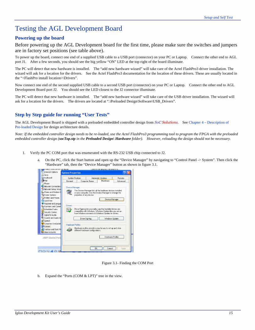
Figure 3.2- Finding the COM Port
c. Note the COM port associated with the “SFE USB to RS232 Controller”. This information will be needed later for running the AGL Development Board tests using the “AGL Board – User Tests” program (GUI).
2. Run the AGL Board User Tests by navigating to the “Preloaded Design\Software\AGL_User_Tests” folder and double clicking the AGL_test.exe file.
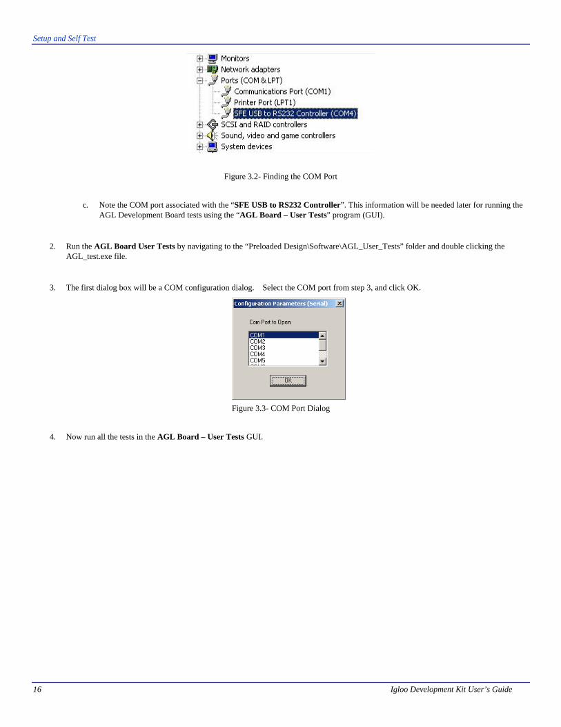
3. The first dialog box will be a COM configuration dialog. Select the COM port from step 3, and click OK.
Figure 3.3- COM Port Dialog
4. Now run all the tests in the AGL Board – User Tests GUI.
Setup and Self Test
Igloo Development Kit User’s Guide 17
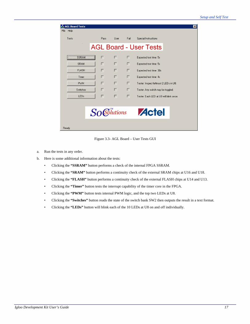
Figure 3.3- AGL Board – User Tests GUI
a. Run the tests in any order.
b. Here is some additional information about the tests:
• Clicking the “SSRAM” button performs a check of the internal FPGA SSRAM.
• Clicking the “SRAM” button performs a continuity check of the external SRAM chips at U16 and U18.
• Clicking the “FLASH” button performs a continuity check of the external FLASH chips at U14 and U13.
• Clicking the “Timer” button tests the interrupt capability of the timer core in the FPGA.
• Clicking the “PWM” button tests internal PWM logic, and the top two LEDs at U8.
• Clicking the “Switches” button reads the state of the switch bank SW2 then outputs the result in a text format.
• Clicking the “LEDs” button will blink each of the 10 LEDs at U8 on and off individually.
Setup and Self Test
18 Igloo Development Kit User’s Guide
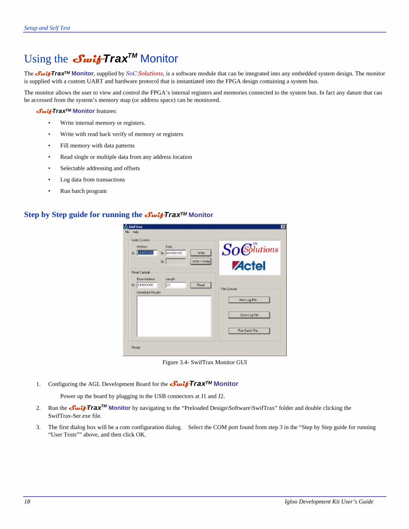
Using the SwifTraxTM Monitor The SwifTraxTM Monitor, supplied by SoC Solutions, is a software module that can be integrated into any embedded system design. The monitor is supplied with a custom UART and hardware protocol that is instantiated into the FPGA design containing a system bus.
The monitor allows the user to view and control the FPGA’s internal registers and memories connected to the system bus. In fact any datum that can be accessed from the system’s memory map (or address space) can be monitored.
SwifTraxTM Monitor features:
• Write internal memory or registers.
• Write with read back verify of memory or registers
• Fill memory with data patterns
• Read single or multiple data from any address location
• Selectable addressing and offsets
• Log data from transactions
• Run batch program
Step by Step guide for running the SwifTraxTM Monitor
Figure 3.4- SwifTrax Monitor GUI
1. Configuring the AGL Development Board for the SwifTraxTM Monitor
Power up the board by plugging in the USB connectors at J1 and J2.
2. Run the SwifTraxTM Monitor by navigating to the “Preloaded Design\Software\SwifTrax” folder and double clicking the SwifTrax-Ser.exe file.
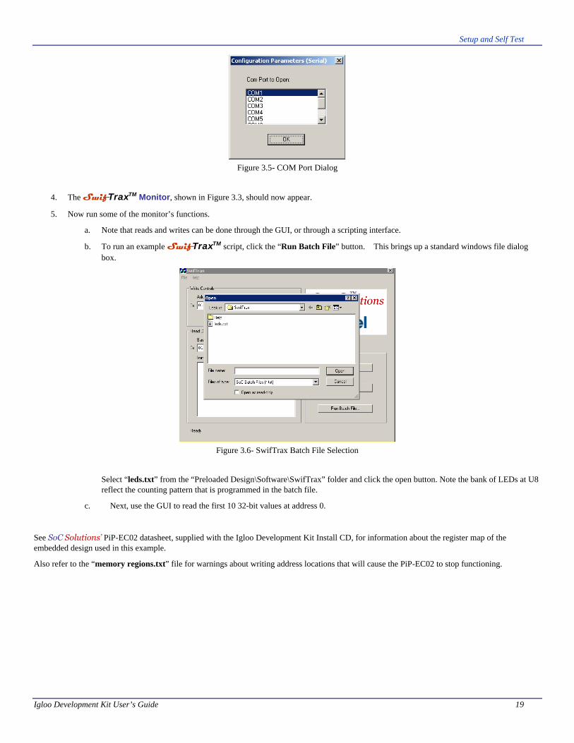
3. The first dialog box will be a com configuration dialog. Select the COM port found from step 3 in the “Step by Step guide for running “User Tests”” above, and then click OK.
Setup and Self Test
Igloo Development Kit User’s Guide 19
Figure 3.5- COM Port Dialog
4. The SwifTraxTM Monitor, shown in Figure 3.3, should now appear.
5. Now run some of the monitor’s functions.
a. Note that reads and writes can be done through the GUI, or through a scripting interface.
b. To run an example SwifTraxTM script, click the “Run Batch File” button. This brings up a standard windows file dialog box.
Figure 3.6- SwifTrax Batch File Selection
Select “leds.txt” from the “Preloaded Design\Software\SwifTrax” folder and click the open button. Note the bank of LEDs at U8 reflect the counting pattern that is programmed in the batch file.
c. Next, use the GUI to read the first 10 32-bit values at address 0.
See SoC Solutions’ PiP-EC02 datasheet, supplied with the Igloo Development Kit Install CD, for information about the register map of the embedded design used in this example.
Also refer to the “memory regions.txt” file for warnings about writing address locations that will cause the PiP-EC02 to stop functioning.
4
Igloo Development Kit User’s Guide 20
Description of the Pre-loaded Design
This is a general description of the embedded controller design, PiP-EC02, that is pre-loaded in the AGL Development Board. The PiP-EC02, Pre-integrated IP platform, is provided by SoC Solutions. The design can be licensed directly from SoC Solutions or CAST, Inc. For more information, contact [email protected] .
PiP-EC02 System Overview
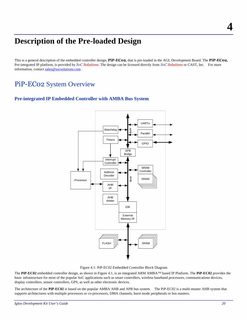
Pre-integrated IP Embedded Controller with AMBA Bus System
Processor
ExternalMemory I/F
Timers
InterruptController
AH
B
FLASHFLASHFLASHFLASH
SRAMSRAMSRAMSRAM
AHBI/F
APBBridge
GPIO
ParallelWatchdog
SRAMController
SRAMSRAMSRAMSRAM
AddressDecoder
UARTs
EBI
AP
B
AHBArbiter
Figure 4.1- PiP-EC02 Embedded Controller Block Diagram
The PiP-EC02 embedded controller design, as shown in Figure 4.1, is an integrated ARM AMBA™ based IP Platform. The PiP-EC02 provides the basic infrastructure for most of the popular SoC applications such as smart controllers, wireless baseband processors, communications devices, display controllers, sensor controllers, GPS, as well as other electronic devices.
The architecture of the PiP-EC02 is based on the popular AMBA AHB and APB bus system. The PiP-EC02 is a multi-master AHB system that supports architectures with multiple processors or co-processors, DMA channels, burst mode peripherals or bus masters.
Description of Pre-loaded Design
Igloo Development Kit User’s Guide 21
As shown in Figure 4.1, the AMBA bus is partitioned into two sections:
1. A high speed AHB bus used for fast memories, DMAs and peripherals.
2. A low speed APB bus used for slower peripherals such as UARTs, GPIO, PWMs, etc.
In this design, there is no embedded processor, so the functionality of a processor is “remoted” to the PC across the serial/USB link. When the software wants to stimulate the hardware design, these requests (reads & writes) are converted by an API into serial commands that are interpreted by a state machine inside the FPGA. This state machine stimulates the AMBA AHB bus in the same way a local embedded processor would..
Note: The pre-loaded PiP-EC02 design does not contain a processor. The pre-loaded design accesses the system bus with the SwifTrax Monitor.
Peripheral Overview
Peripheral Name Verilog Module Name
Bus Description
AHB Arbiter socAhbArb AHB AHB Arbiter for up to three bus masters
Address Decoder socAddrDecRemap AHB Generates block select signals for each system block and provides an address remap utility.
Interrupt Controller socIntrCtrl AHB Monitors all system interrupts and issues interrupt requests to the processor
Internal Memory Interface socIntMemIf AHB Interface to zero wait-state internal synchronous SRAM
External Bus Interface (EBI)
socEbi AHB Provides a configurable interface to external devices such as FLASH and RAM
APB Bridge socApbBridge AHB Bridge from AHB to APB
Timer socTimer APB Time base generator for the system and general-purpose counter. Two used in PiP-EC02.
UART socUart APB Provides a means of asynchronous serial communication with external devices. Two used in PiP-EC02.
Parallel Port socParPort APB PC compatible parallel port
GPIO socGpio APB Configurable general purpose parallel I/O module
PWM SocPwm APB Generates a Pulse-Width-Modulated output
Table 4.1- PiP-EC02 Block descriptions
For more information regarding the pre-loaded embedded controller design, see the PiP-ECO2 datasheet provided in the “Available IP\SoC Solutions” folder or contact SoC Solutions at [email protected].
5
Igloo Development Kit User’s Guide 22
Sample Design Tutorial
This sample design is created specifically for the Actel Igloo Development Kit. This tutorial will guide you through designing, synthesizing, loading and testing using the Libero tools.
Functional Description This sample design will demonstrate the low power modes of the Igloo FPGA. The design just outputs a counting pattern to the LEDs on U8. While this design is rather simple, it will demonstrate the basics of Flash*Freeze and other low power modes.
Hardware Implementation For this sample design project there are three elements that comprise the design.
• Counter
• ULSICC Macro
• I/O
These elements are all contained in the verilog HDL file socTop.v.
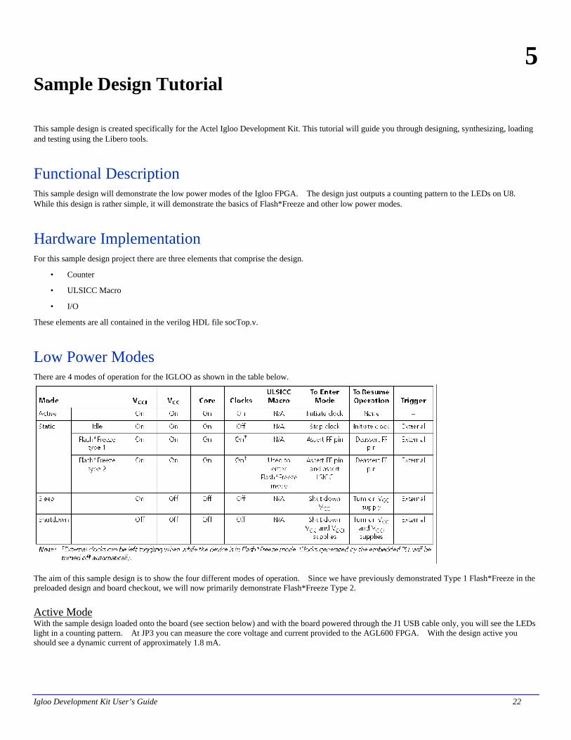
Low Power Modes There are 4 modes of operation for the IGLOO as shown in the table below.
The aim of this sample design is to show the four different modes of operation. Since we have previously demonstrated Type 1 Flash*Freeze in the preloaded design and board checkout, we will now primarily demonstrate Flash*Freeze Type 2. Active Mode With the sample design loaded onto the board (see section below) and with the board powered through the J1 USB cable only, you will see the LEDs light in a counting pattern. At JP3 you can measure the core voltage and current provided to the AGL600 FPGA. With the design active you should see a dynamic current of approximately 1.8 mA.
Sample Design Tutorial
Igloo Development Kit User’s Guide 23
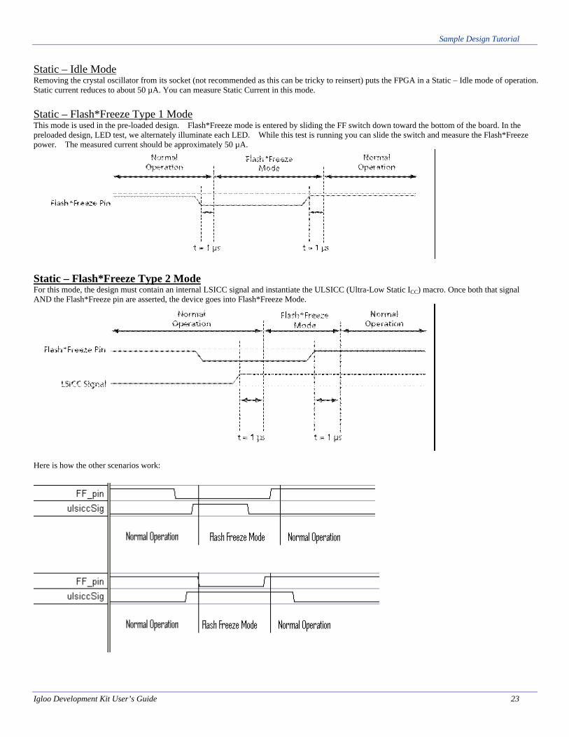
Static – Idle Mode Removing the crystal oscillator from its socket (not recommended as this can be tricky to reinsert) puts the FPGA in a Static – Idle mode of operation. Static current reduces to about 50 µA. You can measure Static Current in this mode. Static – Flash*Freeze Type 1 Mode This mode is used in the pre-loaded design. Flash*Freeze mode is entered by sliding the FF switch down toward the bottom of the board. In the preloaded design, LED test, we alternately illuminate each LED. While this test is running you can slide the switch and measure the Flash*Freeze power. The measured current should be approximately 50 µA.
Static – Flash*Freeze Type 2 Mode For this mode, the design must contain an internal LSICC signal and instantiate the ULSICC (Ultra-Low Static ICC) macro. Once both that signal AND the Flash*Freeze pin are asserted, the device goes into Flash*Freeze Mode.
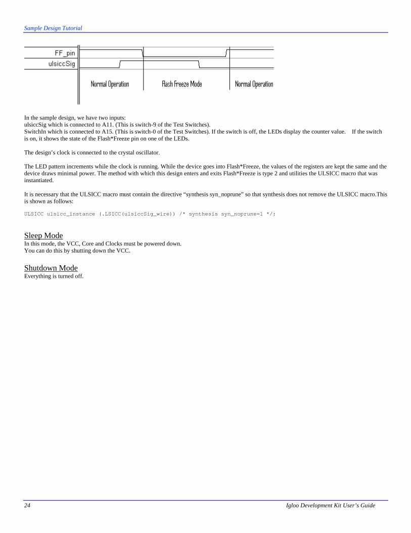
Here is how the other scenarios work:
Sample Design Tutorial
24 Igloo Development Kit User’s Guide
In the sample design, we have two inputs: ulsiccSig which is connected to A11. (This is switch-9 of the Test Switches). SwitchIn which is connected to A15. (This is switch-0 of the Test Switches). If the switch is off, the LEDs display the counter value. If the switch is on, it shows the state of the Flash*Freeze pin on one of the LEDs. The design’s clock is connected to the crystal oscillator. The LED pattern increments while the clock is running. While the device goes into Flash*Freeze, the values of the registers are kept the same and the device draws minimal power. The method with which this design enters and exits Flash*Freeze is type 2 and utilities the ULSICC macro that was instantiated. It is necessary that the ULSICC macro must contain the directive “synthesis syn_noprune” so that synthesis does not remove the ULSICC macro.This is shown as follows: ULSICC ulsicc_instance (.LSICC(ulsiccSig_wire)) /* synthesis syn_noprune=1 */; Sleep Mode In this mode, the VCC, Core and Clocks must be powered down. You can do this by shutting down the VCC. Shutdown Mode Everything is turned off.
Sample Design Tutorial
Igloo Development Kit User’s Guide 25
Sample Design This sample design is created specifically for the Actel Igloo Development Kit. This tutorial will guide you though the following sections:
Sample System Hardware Overview
Libero Project
• Top Level File
• Additional Source Files
• Constraints Files
• Device Options
Program the FPGA on the AGL Development Board
Running the Sample Design
Sample Design Tutorial
26 Igloo Development Kit User’s Guide
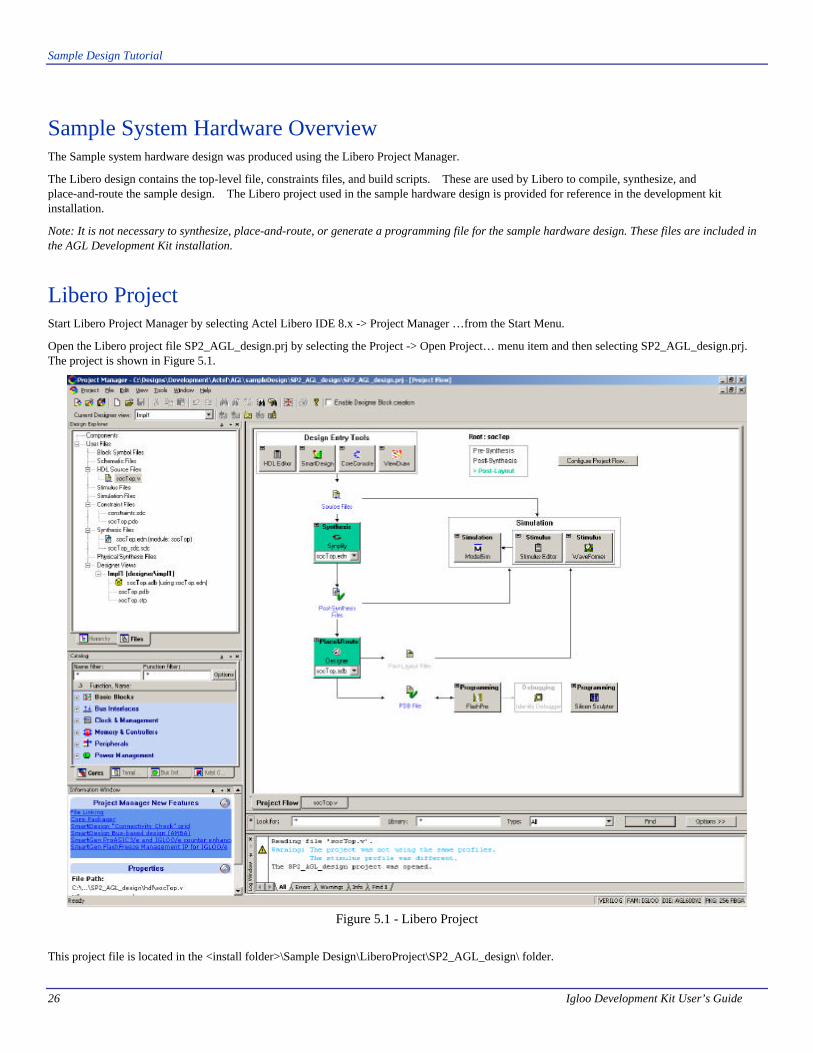
Sample System Hardware Overview The Sample system hardware design was produced using the Libero Project Manager.
The Libero design contains the top-level file, constraints files, and build scripts. These are used by Libero to compile, synthesize, and place-and-route the sample design. The Libero project used in the sample hardware design is provided for reference in the development kit installation.
Note: It is not necessary to synthesize, place-and-route, or generate a programming file for the sample hardware design. These files are included in the AGL Development Kit installation.
Libero Project Start Libero Project Manager by selecting Actel Libero IDE 8.x -> Project Manager …from the Start Menu.
Open the Libero project file SP2_AGL_design.prj by selecting the Project -> Open Project… menu item and then selecting SP2_AGL_design.prj. The project is shown in Figure 5.1.
Figure 5.1 - Libero Project
This project file is located in the <install folder>\Sample Design\LiberoProject\SP2_AGL_design\ folder.
Sample Design Tutorial
Igloo Development Kit User’s Guide 27
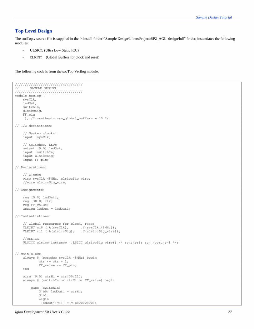
Top Level Design The socTop.v source file is supplied in the “<install folder>\Sample Design\LiberoProject\SP2_AGL_design\hdl” folder, instantiates the following modules:
• ULSICC (Ultra Low Static ICC)
• CLKINT (Global Buffers for clock and reset)
The following code is from the socTop Verilog module.
////////////////////////////////// // SAMPLE DESIGN ////////////////////////////////// module socTop ( sysClk, ledOut, switchIn, ulsiccSig, FF_pin ); /* synthesis syn_global_buffers = 10 */ // I/O definitions: // System clocks: input sysClk; // Switches, LEDs output [9:0] ledOut; input switchIn; input ulsiccSig; input FF_pin; // Declarations: // Clocks wire sysClk_48MHz, ulsiccSig_wire; //wire ulsiccSig_wire; // Assignments: reg [9:0] ledOuti; reg [30:0] ctr; reg FF_value; assign ledOut = ledOuti; // Instantiations: // Global resources for clock, reset CLKINT ci0 (.A(sysClk), .Y(sysClk_48MHz)); CLKINT ci1 (.A(ulsiccSig), .Y(ulsiccSig_wire)); //ULSICC ULSICC ulsicc_instance (.LSICC(ulsiccSig_wire)) /* synthesis syn_noprune=1 */; // Main Block always @ (posedge sysClk_48MHz) begin ctr <= ctr + 1; FF_value <= FF_pin; end wire [9:0] ctrHi = ctr[30:21]; always @ (switchIn or ctrHi or FF_value) begin case (switchIn) 3'b0: ledOuti = ctrHi; 3'b1: begin ledOuti[9:1] = 9'b000000000;
Sample Design Tutorial
28 Igloo Development Kit User’s Guide
ledOuti[0] = FF_value; end endcase end endmodule
Thes file is located in the < install folder>\Sample Design\LiberoProject\SP2_AGL_design\hdl folder.
Constraints Files The following is the list of the Libero Constraint files for the Sample Design:
• constraints.sdc
Timing constraints for synthesis
• socTop.pdc
Physical design constraints for place and route (ie IO placement)
These files are located in the the < install folder>\Sample Design\LiberoProject\SP2_AGL_design\constraints folder.
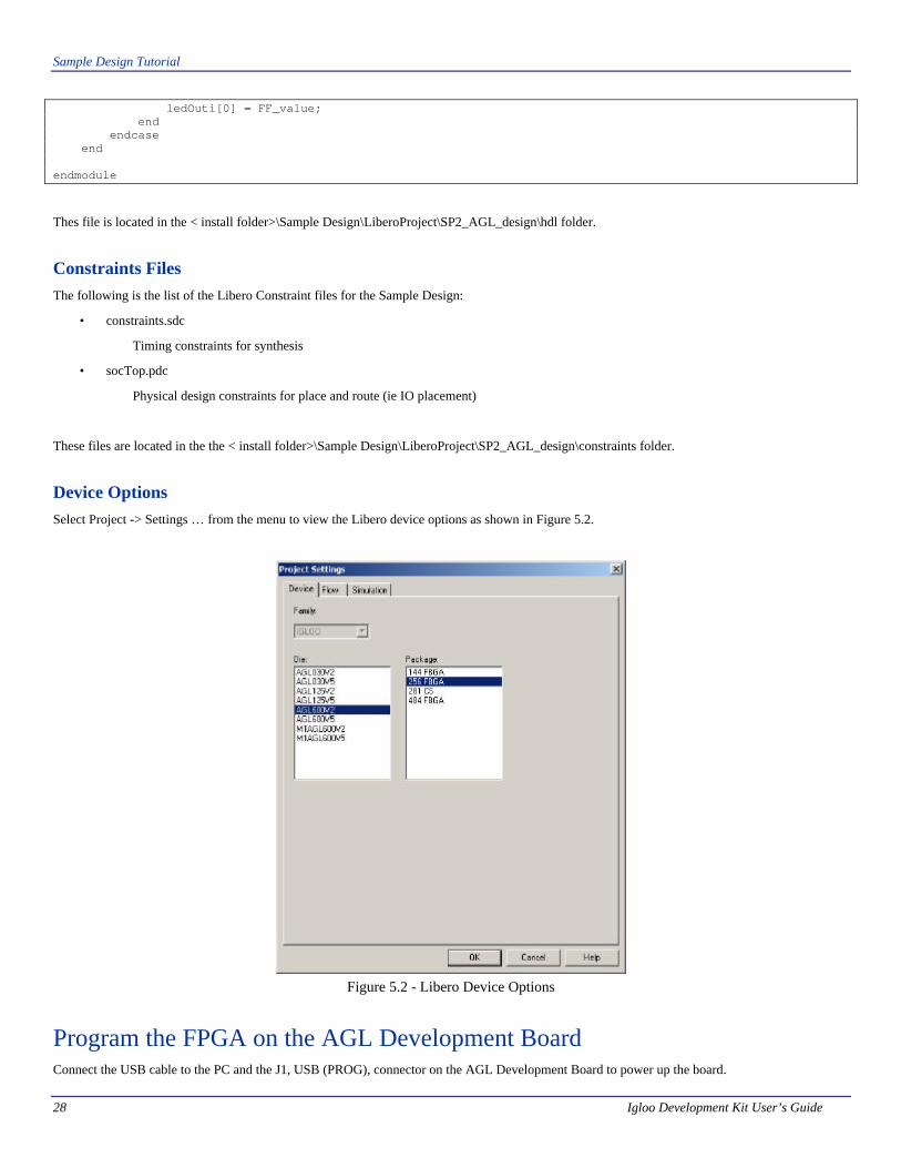
Device Options Select Project -> Settings … from the menu to view the Libero device options as shown in Figure 5.2.
Figure 5.2 - Libero Device Options
Program the FPGA on the AGL Development Board Connect the USB cable to the PC and the J1, USB (PROG), connector on the AGL Development Board to power up the board.
Sample Design Tutorial
Igloo Development Kit User’s Guide 29
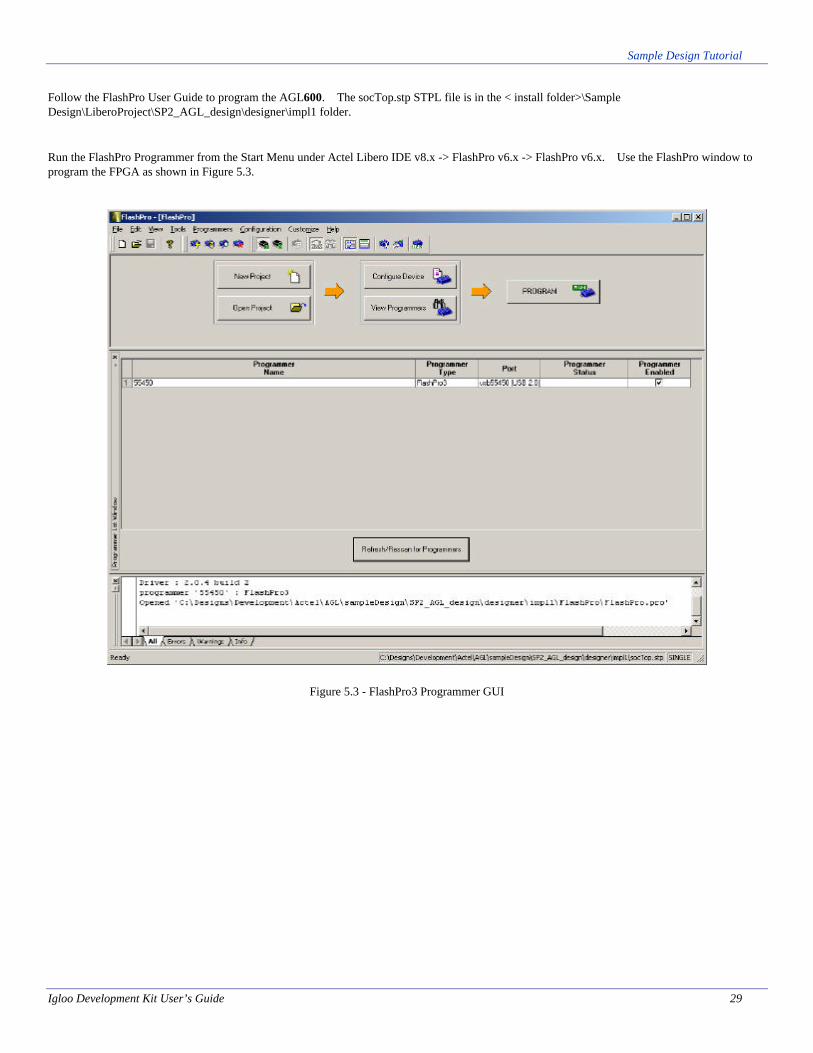
Follow the FlashPro User Guide to program the AGL600. The socTop.stp STPL file is in the < install folder>\Sample Design\LiberoProject\SP2_AGL_design\designer\impl1 folder.
Run the FlashPro Programmer from the Start Menu under Actel Libero IDE v8.x -> FlashPro v6.x -> FlashPro v6.x. Use the FlashPro window to program the FPGA as shown in Figure 5.3.
Figure 5.3 - FlashPro3 Programmer GUI
Sample Design Tutorial
30 Igloo Development Kit User’s Guide
Running the Sample Design The Sample Design Demo showcases the various low power modes available in the Igloo FPGA. Refer to the detailed description in “Low Power Modes” section earlier in this chapter.
The Flash*Freeze pin is mapped to SW3. When SW3 is in the “FF” position, this places the FPGA in Flash*Freeze mode. The ULSICC input signal is mapped to SW2 #9. When SW2 #9 is ON, the ULSICC input signal is alogic ‘1’ state.
The following describes the switch settings to put the IGLOO FPGA in various modes of operation.
Active SW3 NOT in the FF position.
When SW2 #0 is in the “ON” position, the LED at U8 position 0 shows the state of the Flash*Freeze pin as represented by a binary value.
The Flash*Freeze states are as follows:
• LED “ON” indicates “Normal” mode
• LED “OFF” indicates “Flash*Freeze” mode
When SW2 #0 is in the “OFF” position, the design sequences through a counting pattern which is displayed on the LED bank at U8.
Static - Idle SW3 NOT in the FF position, and the oscillator at U20 not installed.
Note: It is recommended that the oscillator not be removed. If it is desired to remove the oscillator, then please take the appropriate precautions. The AGL board is a static-sensitive device.
Warning ! NEVER remove the oscillator when the board is powered up.
Static – Flash*Freeze Type 1 SW2#9 in the “OFF” position and SW3 in the FF position.
Static – Flash*Freeze Type 2 SW2#9 in the “ON” position and SW3 in the FF position.
Refer to the “Low Power Modes” table earlier in this chapter.
A
Igloo Development Kit User’s Guide 31
FG484 & FG256 Packages for the AGL FPGAs
The AGL board uses a 22x22 ball grid array. The FG484 package will use the entire array and the FG256 package does not use the outer 3 rows and columns. Note that this makes the ball grid assignments different. D3 on an FG484 package will be A1 on the FG256. The schematic shows both assignments.
Figure A.1- AGL600 Layout
32 Igloo Development Kit User’s Guide
484-Pin FBGA (Bottom View)
Figure A.2- 484 Pin FBGA Package
Igloo Development Kit User’s Guide 33
256-Pin FBGA (Bottom View)
Figure A.2- 256 Pin FBGA Package
The AGL Development Kit board is designed to accommodate AGL and M1AGL parts in both FG(G)256 and FG(G)484 packages. If the 256 pin BGA is installed the outer 3 rows and columns are not used.
For package manufacturing and environmental information, visit the Packaging Solutions page: http://www.actel.com/products/solutions/default.aspx.
34 Igloo Development Kit User’s Guide
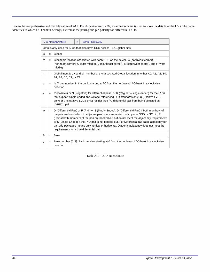
Due to the comprehensive and flexible nature of AGL FPGA device user I / Os, a naming scheme is used to show the details of the I / O. The name identifies to which I / O bank it belongs, as well as the pairing and pin polarity for differential I / Os.
I / O Nomenclature = Gmn / IOuxwBy
Gmn is only used for I / Os that also have CCC access – i.e., global pins.
G = Global
m = Global pin location associated with each CCC on the device: A (northwest corner), B (northeast corner), C (east middle), D (southeast corner), E (southwest corner), and F (west middle)
n = Global input MUX and pin number of the associated Global location m, either A0, A1, A2, B0, B1, B2, C0, C1, or C2
u = I / O pair number in the bank, starting at 00 from the northwest I / O bank in a clockwise direction
x = P (Positive) or N (Negative) for differential pairs, or R (Regular – single-ended) for the I / Os that support single-ended and voltage-referenced I / O standards only. U (Positive-LVDS only) or V (Negative-LVDS only) restrict the I / O differential pair from being selected as LVPECL pair.
w = D (Differential Pair) or P (Pair) or S (Single-Ended). D (Differential Pair) if both members of the pair are bonded out to adjacent pins or are separated only by one GND or NC pin; P (Pair) if both members of the pair are bonded out but do not meet the adjacency requirement; or S (Single-Ended) if the I / O pair is not bonded out. For Differential (D) pairs, adjacency for ball grid packages means only vertical or horizontal. Diagonal adjacency does not meet the requirements for a true differential pair.
B = Bank
y = Bank number [0..3]. Bank number starting at 0 from the northwest I / O bank in a clockwise direction
Table A.1 - I/O Nomenclature
Igloo Development Kit User’s Guide 35
The following table shows the FPGA pin connections to the AGL Development Board signals and the pre-loaded PiP-EC02 design signals.
FG256 Ball FG484 Ball
Pre-loaded Design Signal Schematic Signal I / O Dev. Kit Function
N6 T9 pbRstN BUF2_PBRST_N I Push Button Reset
R4 V7 poRstN PORESET_N I Power on Reset
N4 T7 flashRstN FLASH_RST_N O Reset to Flash Chips
B1 E4 extClk OSC_CLK I System Clock
D6 G9 rs232Atx RS232_TX O UART Transmit
A6 D9 rs232Arx RS232_RX I UART Receive
N3 T6 memAddr[2] MEM_ADDR2 O SRAM / FLASH Address
M4 R7 memAddr[3] MEM_ADDR3 O SRAM / FLASH Address
C5 F8 memAddr[4] MEM_ADDR4 O SRAM / FLASH Address
C6 F9 memAddr[5] MEM_ADDR5 O SRAM / FLASH Address
B4 E7 memAddr[6] MEM_ADDR6 O SRAM / FLASH Address
A4 D7 memAddr[7] MEM_ADDR7 O SRAM / FLASH Address
C2 F5 memAddr[8] MEM_ADDR8 O SRAM / FLASH Address
C1 F4 memAddr[9] MEM_ADDR9 O SRAM / FLASH Address
D4 G7 memAddr[10] MEM_ADDR10 O SRAM / FLASH Address
D2 G5 memAddr[11] MEM_ADDR11 O SRAM / FLASH Address
D1 G4 memAddr[12] MEM_ADDR12 O SRAM / FLASH Address
E4 H7 memAddr[13] MEM_ADDR13 O SRAM / FLASH Address
E3 H6 memAddr[14] MEM_ADDR14 O SRAM / FLASH Address
E2 H5 memAddr[15] MEM_ADDR15 O SRAM / FLASH Address
F2 J5 memAddr[16] MEM_ADDR16 O SRAM / FLASH Address
K1 N4 memAddr[17] MEM_ADDR17 O SRAM / FLASH Address
G4 K7 memAddr[18] MEM_ADDR18 O SRAM / FLASH Address
H5 L8 memAddr[19] MEM_ADDR19 O SRAM / FLASH Address
J5 M8 memAddr[20] MEM_ADDR20 O SRAM / FLASH Address
H3 L6 memAddr[21] MEM_ADDR21 O SRAM / FLASH Address
H1 L4 memAddr[22] MEM_ADDR22 O SRAM / FLASH Address
J1 M4 memAddr[23] MEM_ADDR23 O SRAM / FLASH Address
J2 M5 memAddr[24] MEM_ADDR24 O SRAM / FLASH Address
M2 R5 memAddr[25] MEM_ADDR25 O SRAM / FLASH Address
T8 W11 memData[0] MEM_DATA0 I / O SRAM / FLASH Data
P8 U11 memData[1] MEM_DATA1 I / O SRAM / FLASH Data
R8 V11 memData[2] MEM_DATA2 I / O SRAM / FLASH Data
R7
V10 memData[3] MEM_DATA3 I / O SRAM / FLASH Data
T7 W10 memData[4] MEM_DATA4 I / O SRAM / FLASH Data
P7 U10 memData[5] MEM_DATA5 I / O SRAM / FLASH Data
N8 T11 memData[6] MEM_DATA6 I / O SRAM / FLASH Data
T6 W9 memData[7] MEM_DATA7 I / O SRAM / FLASH Data
R6 V9 memData[8] MEM_DATA8 I / O SRAM / FLASH Data
P6 U9 memData[9] MEM_DATA9 I / O SRAM / FLASH Data
N7 T10 memData[10] MEM_DATA10 I / O SRAM / FLASH Data
T5 W8 memData[11] MEM_DATA11 I / O SRAM / FLASH Data
R5 V8 memData[12] MEM_DATA12 I / O SRAM / FLASH Data
B5 E8 memData[13] MEM_DATA13 I / O SRAM / FLASH Data
T4 W7 memData[14] MEM_DATA14 I / O SRAM / FLASH Data
36 Igloo Development Kit User’s Guide
B6 E9 memData[15] MEM_DATA15 I / O SRAM / FLASH Data
N10 T13 memData[16] MEM_DATA16 I / O SRAM / FLASH Data
T11 W14 memData[17] MEM_DATA17 I / O SRAM / FLASH Data
R11 V14 memData[18] MEM_DATA18 I / O SRAM / FLASH Data
P10 U13 memData[19] MEM_DATA19 I / O SRAM / FLASH Data
T10 W13 memData[20] MEM_DATA20 I / O SRAM / FLASH Data
M9 R12 memData[21] MEM_DATA21 I / O SRAM / FLASH Data
P9 U12 memData[22] MEM_DATA22 I / O SRAM / FLASH Data
R10 V13 memData[23] MEM_DATA23 I / O SRAM / FLASH Data
N9 T12 memData[24] MEM_DATA24 I / O SRAM / FLASH Data
T9 W12 memData[25] MEM_DATA25 I / O SRAM / FLASH Data
R9 V12 memData[26] MEM_DATA26 I / O SRAM / FLASH Data
M8 R11 memData[27] MEM_DATA27 I / O SRAM / FLASH Data
A5 D8 memData[28] MEM_DATA28 I / O SRAM / FLASH Data
C4 F7 memData[29] MEM_DATA29 I / O SRAM / FLASH Data
L3 P6 memData[30] MEM_DATA30 I / O SRAM / FLASH Data
M1 R4 memData[31] MEM_DATA31 I / O SRAM / FLASH Data
N2 T5 flashHiCeN FLASH_HCE_N O Flash Chip Enable (high chip)
M3 R6 flashLoCeN FLASH_LCE_N O Flash Chip Enable (low chip)
L4 P7 flashWeN FLASH_WE_N O Flash Write Enable
N1 T4 flashOeN FLASH_OE_N O Flash Output Enable
N11 T14 sramCeN SRAM_CE_N O SRAM Chip Enable
T14 W17 sramBsN[0] SRBS0_N O SRAM Byte Select 0
R13 V16 sramBsN[1] SRBS1_N O SRAM Byte Select 1
T12 W15 sramBsN[2] SRBS2_N O SRAM Byte Select 2
T13 W16 sramBsN[3] SRBS3_N O SRAM Byte Select 3
R12 V15 sramWeN SRAM_WE_N O SRAM Write Enable
P11 U14 sramOeN SRAM_OE_N O SRAM Output Enable
B7 E10 ledOut[0] LED0 O Drives LED 0
C7 F10 ledOut[1] LED1 O Drives LED 1
P5 U8 ledOut[2] LED2 O Drives LED 2
T2 W5 ledOut[3] LED3 O Drives LED 3
P4 U7 ledOut[4] LED4 O Drives LED 4
R3 V6 ledOut[5] LED5 O Drives LED 5
P2 U5 ledOut[6] LED6 O Drives LED 6
P1 U4 ledOut[7] LED7 O Drives LED 7
R1 V4 ledOut[8] LED8 O Drives LED 8
R2 V5 ledOut[9] LED9 O Drives LED 9
A15 D18 switchIn[0] SWITCH0 I Switch Input 0
A14 D17 switchIn[1] SWITCH1 I Switch Input 1
B14 E17 switchIn[2] SWITCH2 I Switch Input 2
C13 F16 switchIn[3] SWITCH3 I Switch Input 3
A12 D15 switchIn[4] SWITCH4 I Switch Input 4
D11 G14 switchIn[5] SWITCH5 I Switch Input 5
B11 E14 switchIn[6] SWITCH6 I Switch Input 6
C11 F14 switchIn[7] SWITCH7 I Switch Input 7
D10 G13 switchIn[8] SWITCH8 I Switch Input 8
A11 D14 switchIn[9] SWITCH9 I Switch Input 9
Unused Unused gpio0[21:0] Unused I / O General Purpose IO
N13 T16 gpio0[22] GPIOC_29 I / O General Purpose IO
Igloo Development Kit User’s Guide 37
N16 T19 gpio0[23] DIFFB2PRX
I / O General Purpose IO
P16 U19 gpio0[24] DIFFB2NRX I / O General Purpose IO
J14 M17 gpio0[25] DIFFA1P I / O General Purpose IO
K15 N18 gpio0[26] DIFFA1N I / O General Purpose IO
M13 R16 gpio0[27] GPIOC_30 I / O General Purpose IO
L15 P18 gpio0[28] DIFFA2P I / O General Purpose IO
L14 P17 gpio0[29] DIFFA2N I / O General Purpose IO
L16 P19 gpio0[30] DIFFB1P I / O General Purpose IO
M16 R19 gpio0[31] DIFFB1N I / O General Purpose IO
A2 D5 gpio1[0] GPIOA_0 I / O General Purpose IO
A3 D6 gpio1[1] GPIOA_1 I / O General Purpose IO
A7 D10 gpio1[2] GPIOA_2 I / O General Purpose IO
D7 G10 gpio1[3] GPIOA_3 I / O General Purpose IO
D8 G11 gpio1[4] GPIOA_4 I / O General Purpose IO
B8 E11 gpio1[5] GPIOA_5 I / O General Purpose IO
A8 D11 gpio1[6] GPIOA_6 I / O General Purpose IO
C8 F11 gpio1[7] GPIOA_7 I / O General Purpose IO
E8 H11 gpio1[8] GPIOA_8 I / O General Purpose IO
C9 F12 gpio1[9] GPIOA_9 I / O General Purpose IO
B9 E12 gpio1[10] GPIOA_10 I / O General Purpose IO
A9 D12 gpio1[11] GPIOA_11 I / O General Purpose IO
D9 G12 gpio1[12] GPIOA_12 I / O General Purpose IO
E9 H12 gpio1[13] GPIOA_13 I / O General Purpose IO
C10 F13 gpio1[14] GPIOA_14 I / O General Purpose IO
A10 D13 gpio1[15] GPIOA_15 I / O General Purpose IO
B10 E13 gpio1[16] GPIOA_16 I / O General Purpose IO
B13 E16 gpio1[17] GPIOA_17 I / O General Purpose IO
A13 D16 gpio1[18] GPIOA_18 I / O General Purpose IO
C12 F15 gpio1[19] GPIOA_19 I / O General Purpose IO
B12 E15 gpio1[20] GPIOA_20 I / O General Purpose IO
K4 N7 gpio1[21] GPIOA_21 I / O General Purpose IO
K2 N5 gpio1[22] GPIOA_22 I / O General Purpose IO
J4 M7 gpio1[23] GPIOA_23 I / O General Purpose IO
G1 K4 gpio1[24] GPIOA_24 I / O General Purpose IO
G2 K5 gpio1[25] GPIOA_25 I / O General Purpose IO
G3 K6 gpio1[26] GPIOA_26 I / O General Purpose IO
F4 J7 gpio1[27] GPIOA_27 I / O General Purpose IO
F3 J6 gpio1[28] GPIOA_28 I / O General Purpose IO
F1 J4 gpio1[29] GPIOA_29 I / O General Purpose IO
E1 H4 gpio1[30] GPIOA_30 I / O General Purpose IO
B2 E5 gpio1[31] GPIOA_31 I / O General Purpose IO
E13 H16 gpio2[0] GPIOB_0 I / O 2.5V IO
C16 F19 gpio2[1] GPIOB_1 I / O
D16 G19 gpio2[2] GPIOB_2 I / O
LVDS IO Transmit Pair with termination
G15 K18 gpio2[3] GPIOB_3 I / O
G16 K19 gpio2[4] GPIOB_4 I / O
LVDS IO Transmit Pair with termination
E16 J18 gpio2[5] GPIOBRX_5 I / O
F16 K17 gpio2[6] GPIOBRX_6 I / O
LVDS IO Receive Pair with termination
38 Igloo Development Kit User’s Guide
B15 E18 gpio2[7] GPIOB_7 I / O
B16 E19 gpio2[8] GPIOB_8 I / O
LVDS IO Transmit Pair with termination
D14 G17 gpio2[9] GPIOB_9 I / O
C15 F18 gpio2[10] GPIOB_10 I / O
LVDS IO Transmit Pair with termination
E14 H17 gpio2[11] GPIOBRX_11 I / O
H15 L18 gpio2[12] GPIOBRX_12 I / O
LVDS IO Receive Pair with termination
E15 H18 gpio2[13] GPIOB_13 I / O
F14 J17 gpio2[14] GPIOB_14 I / O
LVDS IO Transmit Pair with termination
F15 J18 gpio2[15] GPIOB_15 I / O
G14 K17 gpio2[16] GPIOB_16 I / O
LVDS IO Transmit Pair with termination
J15 M18 gpio2[17] GPIOBRX_17 I / O
K14 N17 gpio2[18] GPIOBRX_18 I / O
LVDS IO Receive Pair with termination
G13 K16 gpio2[19] GPIOB_19 I / O
H12 L15 gpio2[20] GPIOB_20 I / O
LVDS IO Transmit Pair with termination
H13 L16 gpio2[21] GPIOB_21 I / O
H16 L19 gpio2[22] GPIOB_22 I / O
LVDS IO Transmit Pair with termination
J13 M16 gpio2[23] GPIOBRX_23 I / O
H14 L17 gpio2[24] GPIOBRX_24 I / O
LVDS IO Receive Pair with termination
J16 M19 gpio2[25] GPIOB_25 I / O
K16 N19 gpio2[26] GPIOB_26 I / O
LVDS IO Transmit Pair with termination
M14 R17 gpio2[27] GPIOB_27 I / O
L13 P16 gpio2[28] GPIOB_28 I / O
LVDS IO Transmit Pair with termination
M15 R18 gpio2[29] GPIOBRX_29 I / O
N15 T18 gpio2[30] GPIOBRX_30 I / O
LVDS IO Receive Pair with termination
F13 J16 gpio2[31] GPIOB_31 I / O 2.5V IO
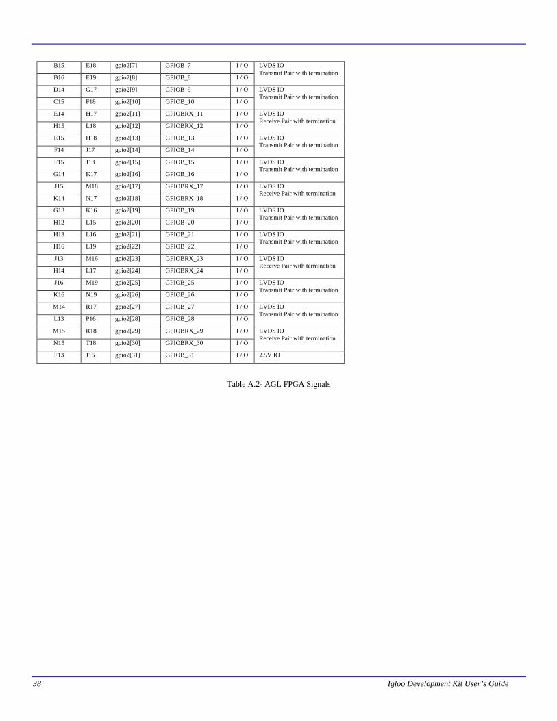
Table A.2- AGL FPGA Signals
B
Igloo Development Kit User’s Guide 39
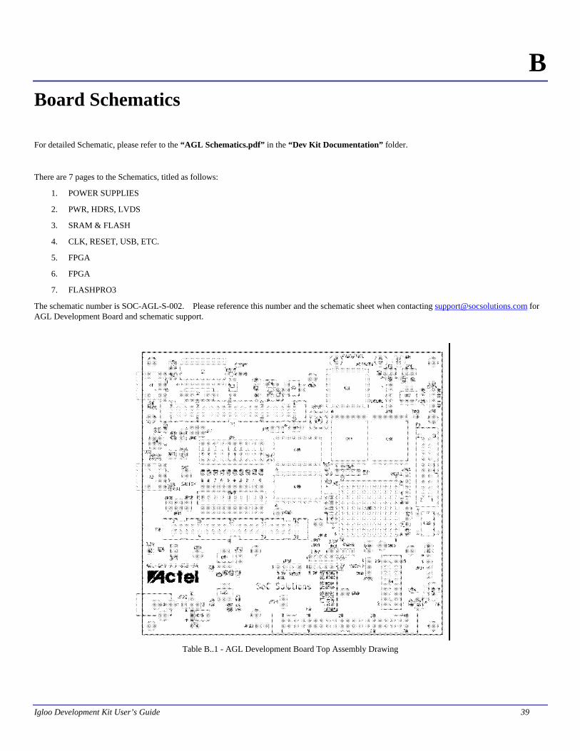
Board Schematics
For detailed Schematic, please refer to the “AGL Schematics.pdf” in the “Dev Kit Documentation” folder.
There are 7 pages to the Schematics, titled as follows:
1. POWER SUPPLIES
2. PWR, HDRS, LVDS
3. SRAM & FLASH
4. CLK, RESET, USB, ETC.
5. FPGA
6. FPGA
7. FLASHPRO3
The schematic number is SOC-AGL-S-002. Please reference this number and the schematic sheet when contacting [email protected] for AGL Development Board and schematic support.
Table B..1 - AGL Development Board Top Assembly Drawing
C
Igloo Development Kit User’s Guide 40
Product Support
SoC Solutions is providing technical and non-technical support for this product. The product is distributed through Actel and its distributors. For pricing information, please contact Actel. For all other support, please contact SoC Solutions by email or phone.
Technical Support
Email You can communicate your technical questions to our email address and receive answers back by email, fax, or phone. Also, if you have design problems, you can email your design files to receive assistance. We constantly monitor the email account throughout the day. When sending your request to us, please be sure to include your full name, company name, and your contact information for efficient processing of your request.
The technical support email address is [email protected].
Phone Our Support Staff can help you with hardware, software and installation issues. SoC Solutions will retrieve information, such as your name, company name, phone number and your question, and then issues a case number. The phone hours are from 10:00 A.M. to 6:00 P.M., Eastern Time, Monday through Friday. The Technical Support numbers are:
770-680-2500 Ask for technical support for Actel.
Customers needing assistance outside the US time zones can either contact technical support via email [email protected].