Embed Size (px)
Citation preview

IGBT Module Application for HighPower Density Design
- 2011/08

Page 2Copyright © Infineon Technologies 2006. All rights reserved.
Table of contents
High power density & IGBT module development
IGBT safe operational area & the design principle
Reliability requirement & estimation
High power density on CAV and wind power application
Page 3Copyright © Infineon Technologies 2006. All rights reserved.
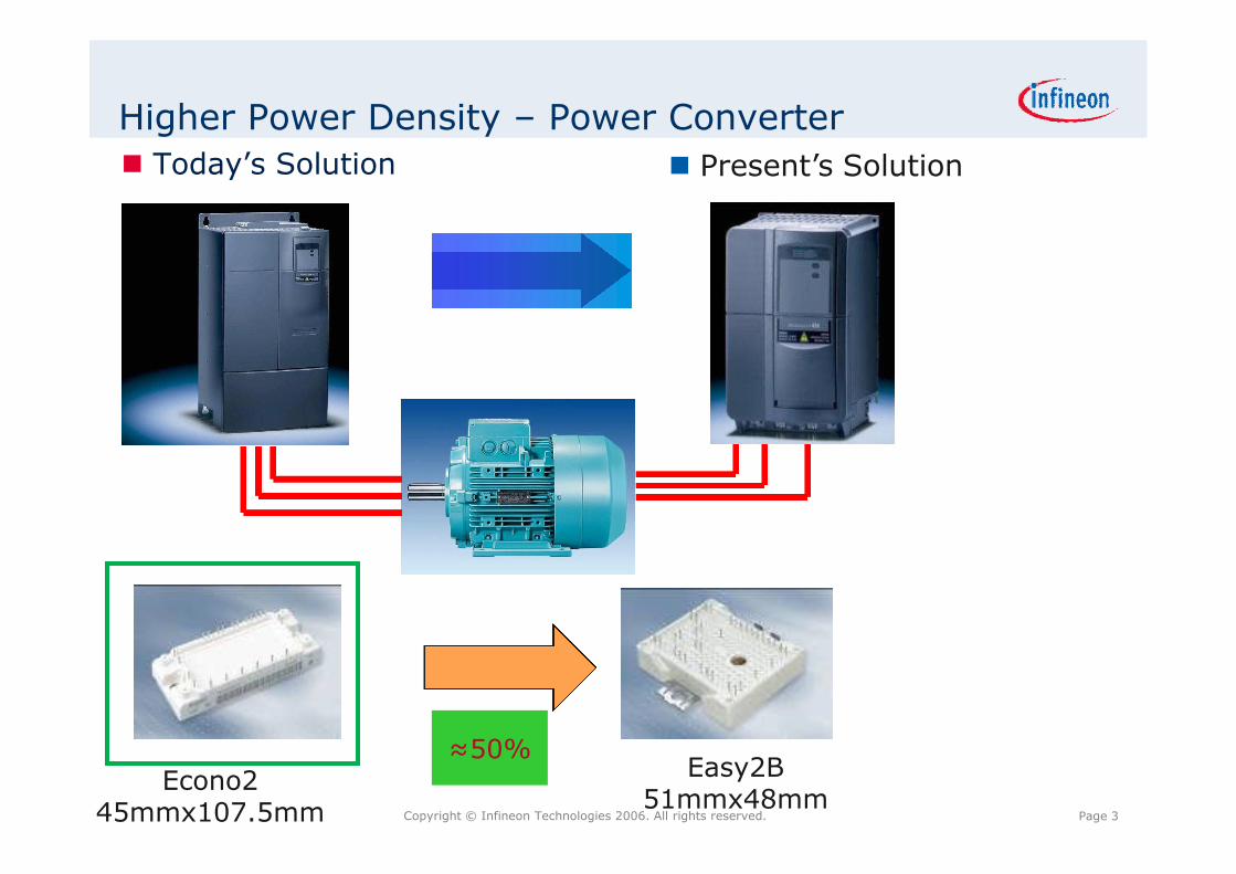
Higher Power Density – Power Converter
Today’s Solution Present’s Solution
Easy2B51mmx48mm
Econo245mmx107.5mm
≈50%
Page 4Copyright © Infineon Technologies 2006. All rights reserved.
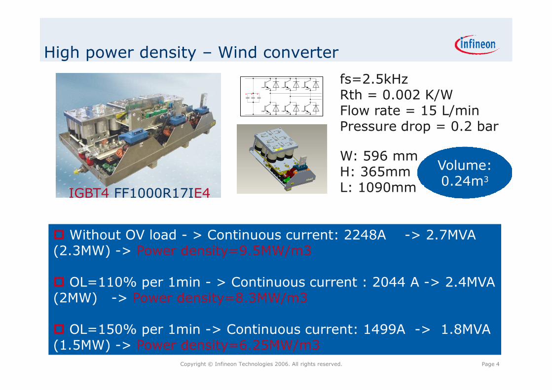
High power density – Wind converter
Without OV load - > Continuous current: 2248A -> 2.7MVA(2.3MW) -> Power density=9.5MW/m3
OL=110% per 1min - > Continuous current : 2044 A -> 2.4MVA(2MW) -> Power density=8.3MW/m3
OL=150% per 1min -> Continuous current: 1499A -> 1.8MVA(1.5MW) -> Power density=6.25MW/m3
fs=2.5kHzRth = 0.002 K/WFlow rate = 15 L/minPressure drop = 0.2 bar
W: 596 mmH: 365mmL: 1090mmIGBT4 FF1000R17IE4
Volume:0.24m3
Page 5Copyright © Infineon Technologies 2006. All rights reserved.
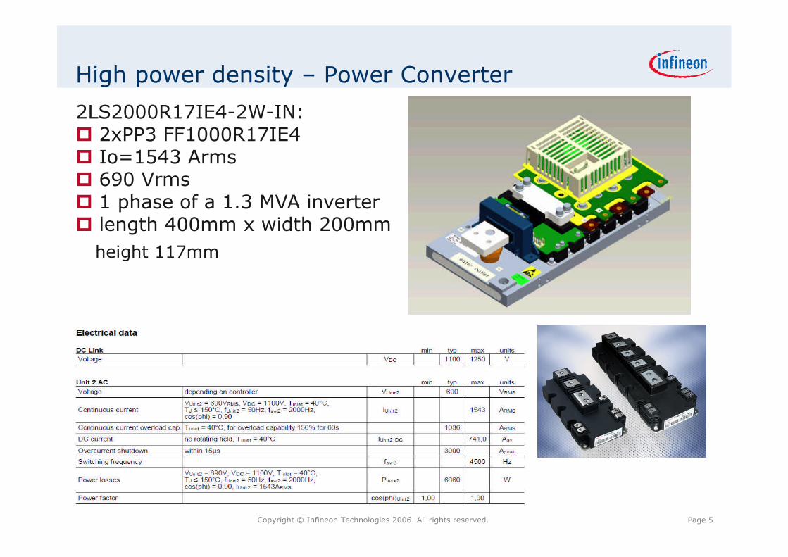
High power density – Power Converter
2LS2000R17IE4-2W-IN: 2xPP3 FF1000R17IE4 Io=1543 Arms 690 Vrms 1 phase of a 1.3 MVA inverter length 400mm x width 200mm
height 117mm

Page 6Copyright © Infineon Technologies 2006. All rights reserved.
High power density – PrimeSTACK
RMS Io=234A, fs=3kHz, fo=50Hz, L=280mm,W=216mm, H=75mm Air forcedAir flow: Min. 485m3/h,Pressure drop: 410pa (Typ.)Airinlet: -25oC~40oC
FF300R12KE3 Estimated heatsink Rthha =0.02114K/WRthha per module=0.0634K/W
Power:120kW
5.29MW/m3
0.0227m3
Page 7Copyright © Infineon Technologies 2006. All rights reserved.
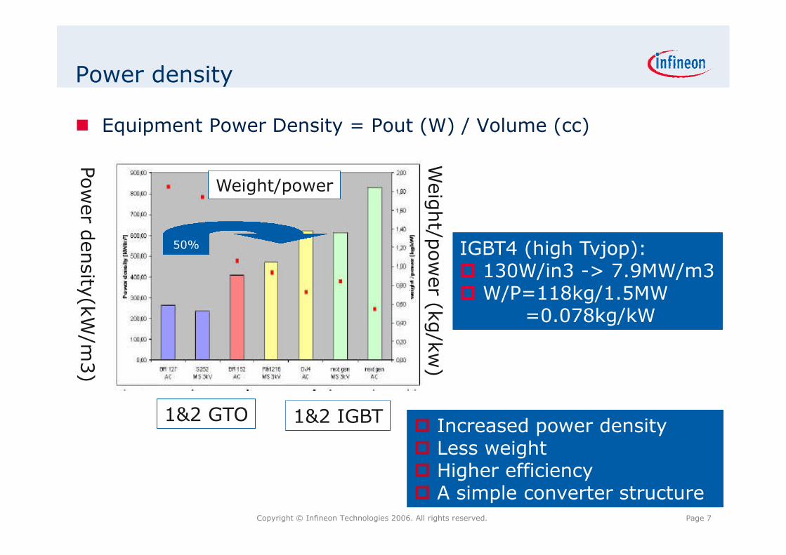
Power density
Equipment Power Density = Pout (W) / Volume (cc)
Weight/power
Pow
er
density
(kW
/m3)
Weig
ht/p
ow
er
(kg/k
w)
1&2 GTO 1&2 IGBT
50%
Increased power density Less weight Higher efficiency A simple converter structure
IGBT4 (high Tvjop): 130W/in3 -> 7.9MW/m3 W/P=118kg/1.5MW
=0.078kg/kW

Page 8Copyright © Infineon Technologies 2006. All rights reserved.
IGBT - High power density
Power density
IGBT modulechip/package
Coolingthermal design
Constructionlayout/
optimization
Driving approachswitching/gate
driving
Sub – system(Topology, Application etc)
Page 9Copyright © Infineon Technologies 2006. All rights reserved.
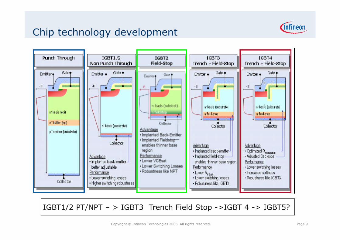
Chip technology development
IGBT1/2 PT/NPT – > IGBT3 Trench Field Stop ->IGBT 4 -> IGBT5?

Page 10Copyright © Infineon Technologies 2006. All rights reserved.
1 2 3 4 5
tota
lsw
itchin
glo
sses
Saturation voltage VCEsat [V]
IGBT2 – KS4
IGBT2 – DN2
IGBT2 – DLCIGBT3 – E3
IGBT3 – T3
1200V IGBT Chip generation Trade-Off
E4 - IGBT4 Medium Power
P4 - IGBT4 High Power
T4 - IGBT4 Low Power
Typical values @ Tvj=125°C
-20% Eoff
E4
P4
IGBT4 High Power: improved softnessIGBT4 Medium Power: lower switching losses than E3 with the same softnessIGBT4 Low Power: lower switching losses than T3 with the same switching characteristic
-15% Eoff
T4
The information given in this presentation is given as a hint for the implementation of the Infineon Technologies components only and shall not be regarded as any description of warranty of a certainfunctionality, conditions or quality of the Infineon Technologies components. The statements contained in this communication, including any recommendation or suggestion or methodology, are to beverified by the user before implementation, as operating conditions and environmental factors may differ. The recipient of this presentation must verify any function described herein in the realapplication. Infineon Technologies hereby disclaims any and all warranties and liabilities of any kind (including without limitation warranties of non-infringement of intellectual property rights of anythird party) with respect to any and all information given in this presentation.

Page 11Copyright © Infineon Technologies 2006. All rights reserved.
IGBT chip development trendpast/present /future
1
1.5
2
2.5
3
3.5
4
1988 1992 1996 2000 2004 2008 2012
VC
Esat(
125°C
)[V
]@
75A
1st Gen
2nd Gen 3rd Gen 4th Gen 5th Gen
A/A0 = 1 A/A0 =65
A/A0 = 0,44A/A0 = 0,39
A/A0 = 0,31
1200 V / 75 A IGBT
Nennschaltleistung: 100 kW
Kurzschlußleistung: 500 kW
Optimized trade-off behavior between conduction and switching losses
Increase of operational junction temperature by 25K
Reduction of chip area
125°C
150°C175°C
Page 12Copyright © Infineon Technologies 2006. All rights reserved.
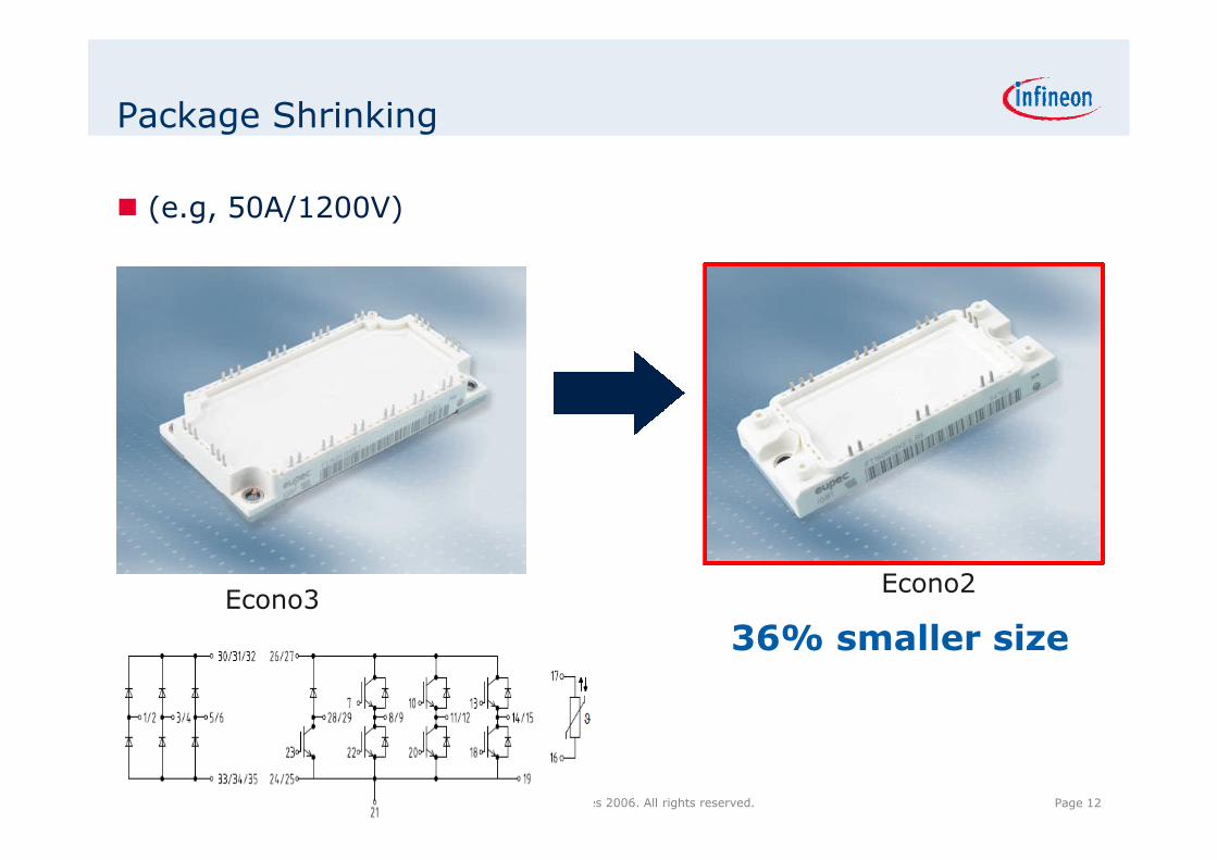
Package Shrinking
(e.g, 50A/1200V)
Econo3Econo2
36% smaller size
Page 13Copyright © Infineon Technologies 2006. All rights reserved.
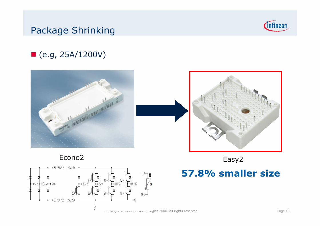
Package Shrinking
(e.g, 25A/1200V)
Econo2 Easy2
57.8% smaller size

Page 14Copyright © Infineon Technologies 2006. All rights reserved.
Package Shrinking
FS150R12KT4
SixPACK
FS100R12PT4FS150R12PT4FS200R12PT4
EconoPACK4 Econo3
Page 15Copyright © Infineon Technologies 2006. All rights reserved.
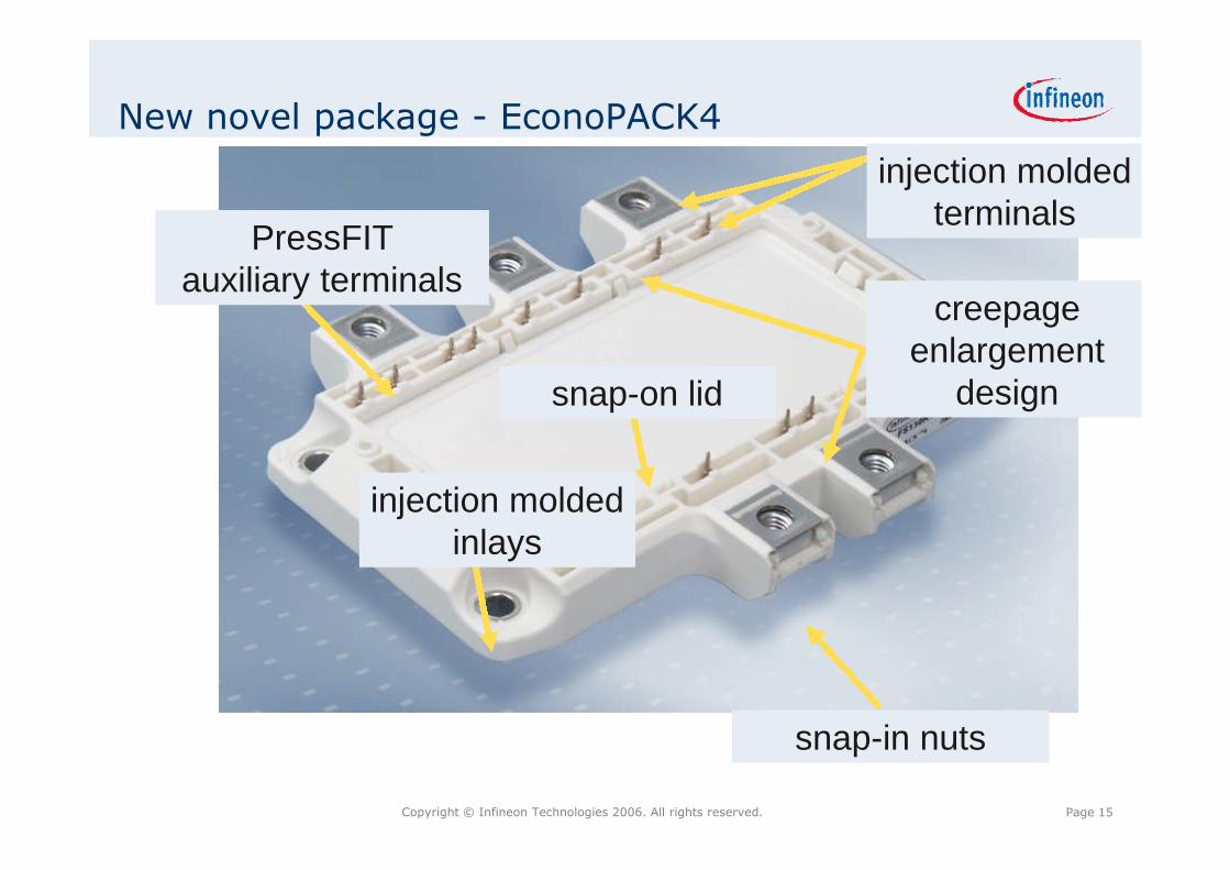
New novel package - EconoPACK4
PressFITauxiliary terminals
injection moldedterminals
snap-on lid
injection moldedinlays
creepageenlargement
design
snap-in nuts
Page 16Copyright © Infineon Technologies 2006. All rights reserved.
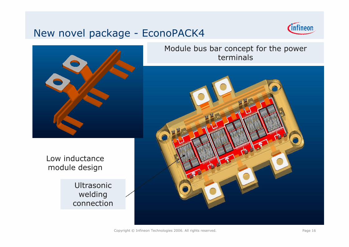
New novel package - EconoPACK4
Module bus bar concept for the powerterminals
Low inductancemodule design
Ultrasonicwelding
connection

Page 17Copyright © Infineon Technologies 2006. All rights reserved.
Package Current Extension – Econo3
SixPACKFS150R12KT4FS100R12KT3
62mmx 122mmx 17mm

Page 18Copyright © Infineon Technologies 2006. All rights reserved.
Package Current Extension - EconoDUAL3
1200V/600A1700V/600A
1200V/450A1700V/450A
62mmx 122mmx 17mm
Half bridge
Page 19Copyright © Infineon Technologies 2006. All rights reserved.
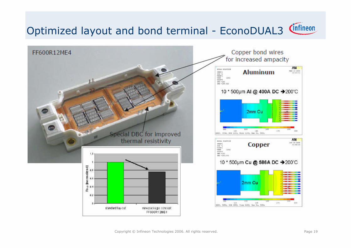
Optimized layout and bond terminal - EconoDUAL3

Page 20Copyright © Infineon Technologies 2006. All rights reserved.
Package Current Extension - PrimePACK3
FF1400R17IP41400A / 1700V
FF1000R17IE41000A / 1700V
1400A/IP4
Vcesat =2.1V @Tvj=125oC2.2V @Tvj=150oC
(Eon+Eoff) /Inom =0.804mJ/A Rthjc=0.0155K/W
1000A/IE4
Vcesat =2.35V @Tvj=125oC2.45V @Tvj=150oC
(Eon+Eoff)/Inom=0.681mJ/A Rthjc=0.024K/W

Page 21Copyright © Infineon Technologies 2006. All rights reserved.
Table of contents
High power density & IGBT module development
IGBT safe operational area & the design principle
Reliability requirement & estimation
High power density on CAV and wind power application
Page 22Copyright © Infineon Technologies 2006. All rights reserved.
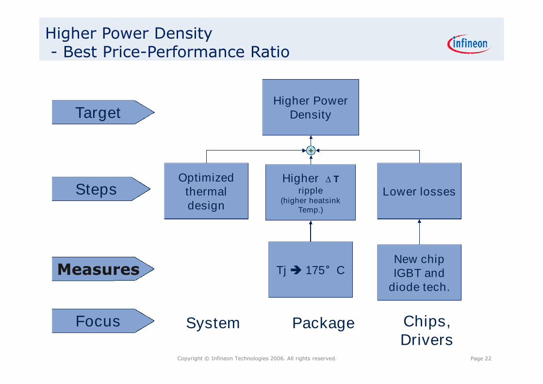
Higher Power Density- Best Price-Performance Ratio
Higher PowerDensity
Optimizedthermaldesign
Higher ∆ T
ripple(higher heatsink
Temp.)
Lower losses
+
Measures Tj 175°CNew chipIGBT and
diode tech.
Focus
Steps
Target
System Chips,Drivers
Package
Page 23Copyright © Infineon Technologies 2006. All rights reserved.
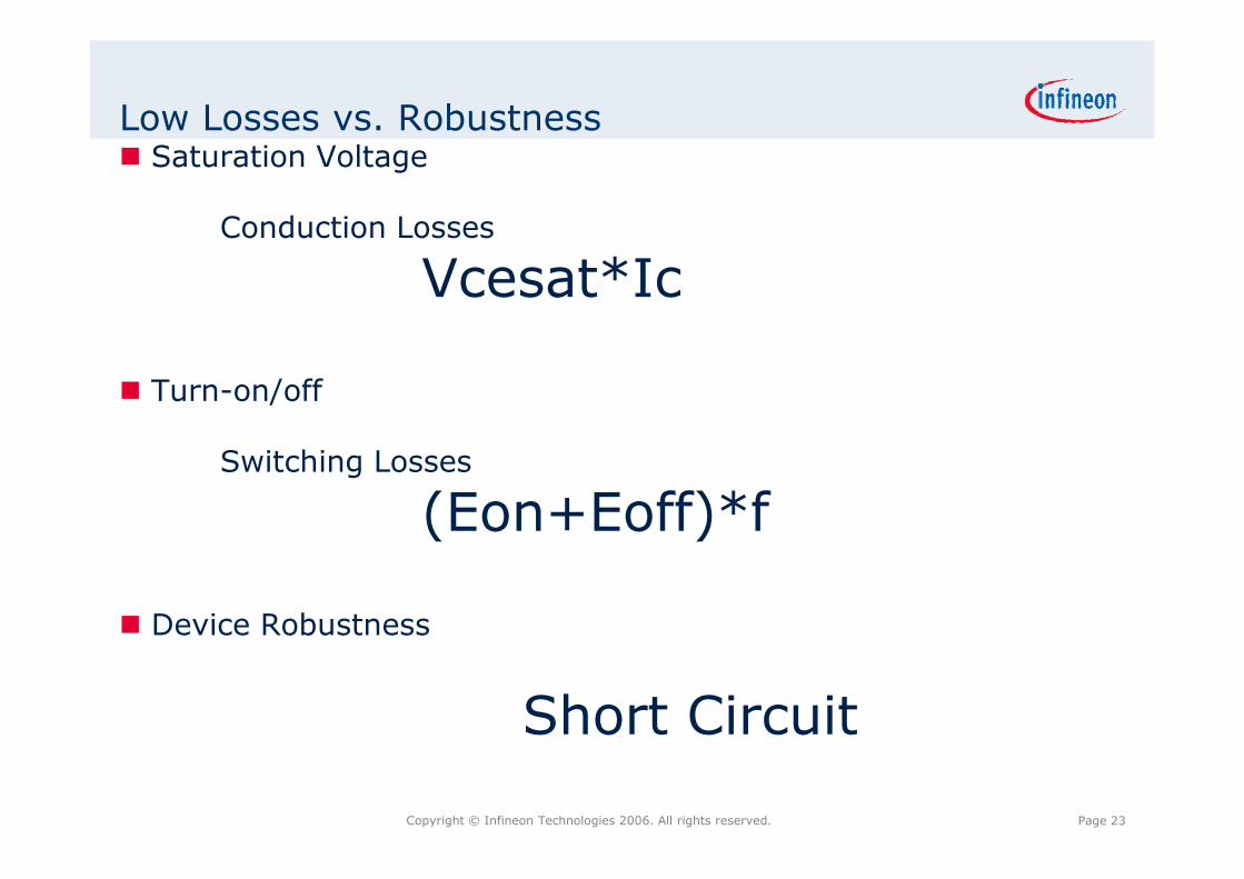
Low Losses vs. Robustness Saturation Voltage
Conduction Losses
Vcesat*Ic
Turn-on/off
Switching Losses
(Eon+Eoff)*f
Device Robustness
Short Circuit
Page 24Copyright © Infineon Technologies 2006. All rights reserved.
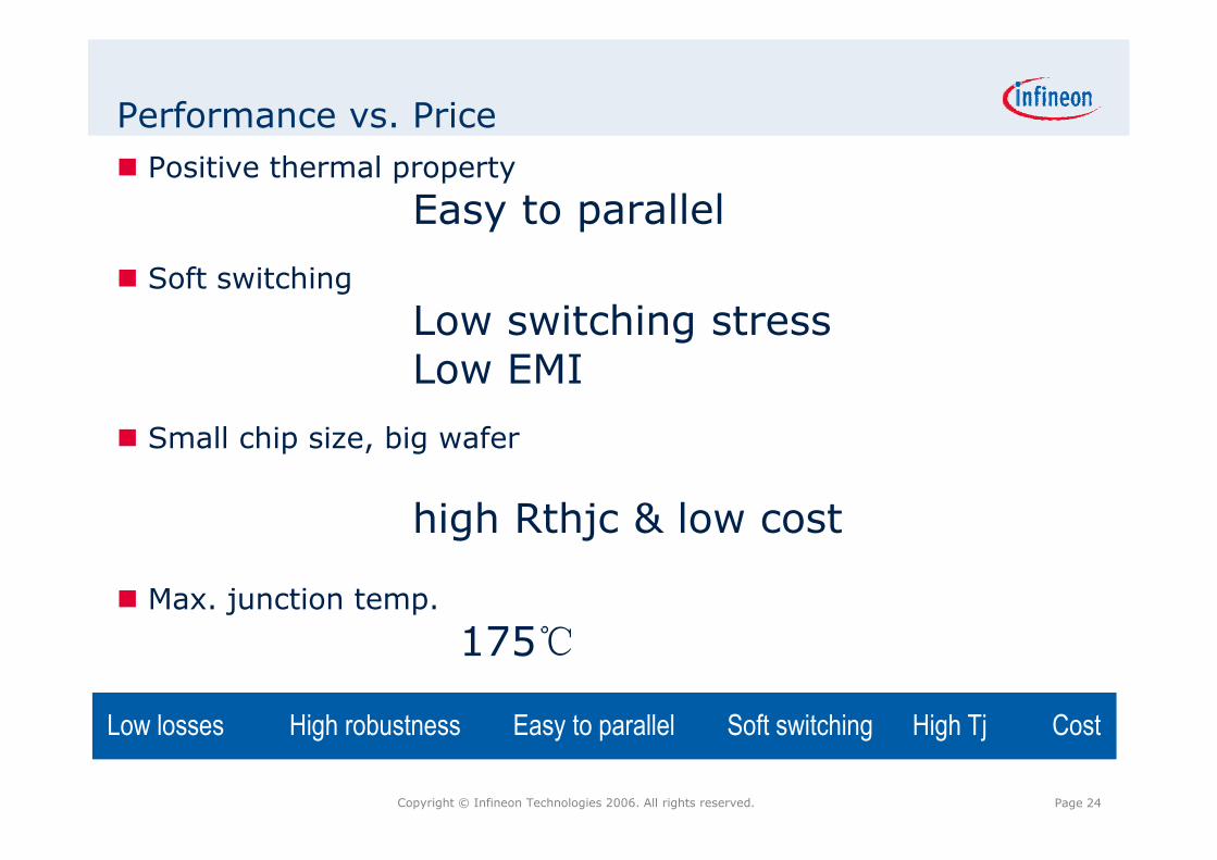
Performance vs. Price
Positive thermal property
Easy to parallel
Soft switching
Low switching stressLow EMI
Small chip size, big wafer
high Rthjc & low cost
Max. junction temp.
175℃
Low losses High robustness Easy to parallel Soft switching High Tj Cost

Page 25Copyright © Infineon Technologies 2006. All rights reserved.
• IGBT Safe Operation Area
•Thermal Limit
•Mechanical Requirement
•Reliability Requirement
IGBT selection for high power density
Page 26Copyright © Infineon Technologies 2006. All rights reserved.
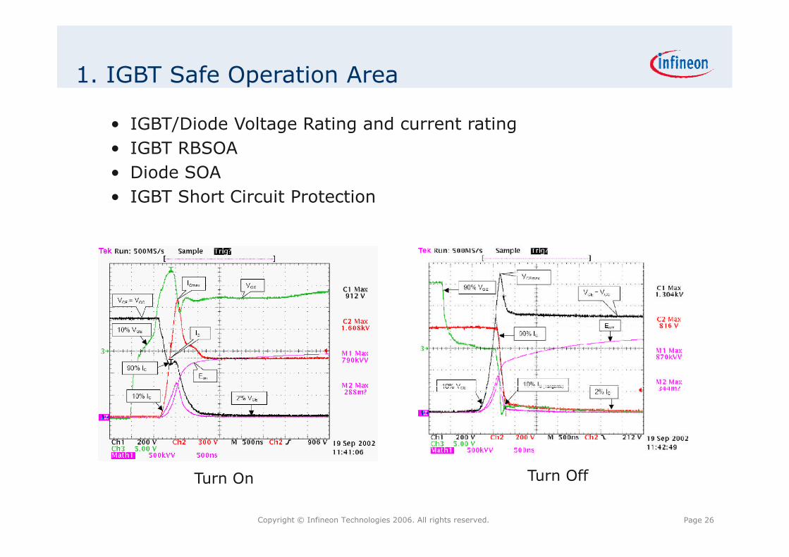
1. IGBT Safe Operation Area
Turn On Turn Off
• IGBT/Diode Voltage Rating and current rating
• IGBT RBSOA
• Diode SOA
• IGBT Short Circuit Protection

Page 27Copyright © Infineon Technologies 2006. All rights reserved.
2. Thermal Limit – Junction Temperature

Page 28Copyright © Infineon Technologies 2006. All rights reserved.
2. Thermal Limit – Pulse Power
ΔTj ΔTj
Fundamental frequency: 50HzTemperature swing in the IGBTTemperature swing in the diode
Fundamental frequency: 1HzTemperature swing in the IGBTTemperature swing in the diode
Thermal Impedance

Page 29Copyright © Infineon Technologies 2006. All rights reserved.
Material Group of EconoDUAL™3package withCTI > 200 Material group IIIa
Material Group / Isolierstoffklasse
Material group I: 600 ≤ CTI
Material group II: 400 ≤ CTI ≤ 600
Material group IIIa: 175 ≤ CTI < 400
Material group IIIb: 100 ≤ CTI ≤ 175
CTIUL
(PLC) IEC
600 < CTI 0 I
400 ≤ CTI < 600 1 II
250 ≤ CTI < 400 2IIIa
175 ≤ CTI < 250 3
100 ≤ CTI < 175 4 IIIb
0 < CTI < 100 5 -
e.g. EconoDUAL™3 housing material group
3. Package Requirements - insulation

Page 30Copyright © Infineon Technologies 2006. All rights reserved.
3. Package Requirements – busbar design
Driver/Boosterboard
AC-terminal Low inductive 2- or3-layer busbar
HeatsinkDC link capacitors, mountedclose to the module
Page 31Copyright © Infineon Technologies 2006. All rights reserved.
× ×
×
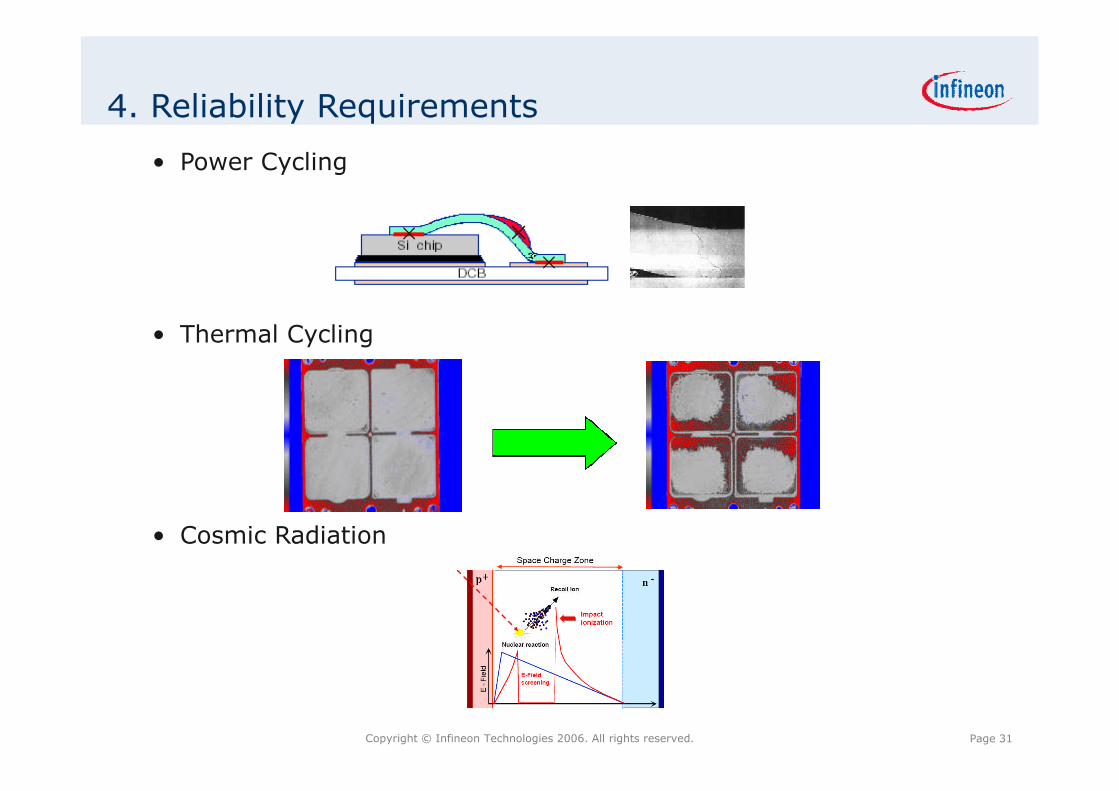
4. Reliability Requirements
• Power Cycling
• Thermal Cycling
• Cosmic Radiation

Page 32Copyright © Infineon Technologies 2006. All rights reserved.
IGBT Safe Operation – IGBT RBSOA
Pulse current (ICRM IRBSOA)
ICRM is defined as repetitive turn on pulse current, related to IGBT thermal
IRBSOA is defined as maximum turn off current
ICRM
IRBSOA
1ms is just test condition, real pulse width is depend on thermal
VCEIC VGE
ICRM may be exceeded during turn on due to reverse recovery.

Page 33Copyright © Infineon Technologies 2006. All rights reserved.
DC linkvoltage
IGBT Safe Operation – IGBT RBSOA
Blocking voltage (VCES)
VCES can not be violated at any condition, otherwise IGBT wouldbreak though
VCES specified at Tj=25℃. Higher Tj, higher blocking voltage
Due to stray inductance inside module
Chip level
Module level
VCES is easiest to be exceed duringturn off, due to external and internalstray inductance
LdtdiV */

Page 34Copyright © Infineon Technologies 2006. All rights reserved.
IGBT Safe Operation - RBSOA
For 3rd and 4th IGBT, Rgoff has little impact on Eoff, dv/dt, and di/dt di/dt is only controllable if the gate voltage doesn’t drop below the Miller Plateau
level before IC starts to decrease dv/dt and di/dt are controllable by the gate resistor when Rgoff is very large A larger resistor will result in a smaller dv/dt and di/dt

Page 35Copyright © Infineon Technologies 2006. All rights reserved.
IGBT Safe Operation – Diode SOA
Blocking voltage (VRRM)
Pulse current (ICRM)
Similar definition of VCES at Tj25℃
Similar definition of ICRM , two time of IF.
Page 36Copyright © Infineon Technologies 2006. All rights reserved.
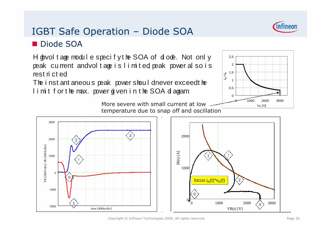
IGBT Safe Operation – Diode SOA
Diode SOA
0
0,5
1
1,5
2
2,5
0 1000 2000 3000
VR [V]
2000
1000
0
1000
2000
3000
time [400ns/div]
VR
[50
0V
/div
]IR
[50
0A
/div
]
1
23
!
0
0 1000 2000 30000
1000
2000
VR(t) [V]
IR(t
)[A
]locus iR(t)*vR(t)
1
2
3
!
0
High voltage module specify the SOA of diode. Not onlypeak current and voltage is limited, peak power also isrestricted.The instantaneous peak power should never exceed thelimit for the max. power given in the SOA diagram.
More severe with small current at lowtemperature due to snap off and oscillation
Page 37Copyright © Infineon Technologies 2006. All rights reserved.
IGBT Safe Operation - Diode SOA
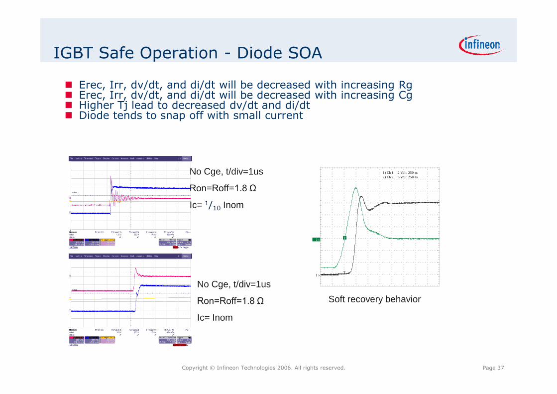
Erec, Irr, dv/dt, and di/dt will be decreased with increasing Rg Erec, Irr, dv/dt, and di/dt will be decreased with increasing Cg Higher Tj lead to decreased dv/dt and di/dt Diode tends to snap off with small current
No Cge, t/div=1us
Ron=Roff=1.8 Ω
Ic= 1/10 Inom
No Cge, t/div=1us
Ron=Roff=1.8 Ω
Ic= Inom
T
T
1 >
2 >
1) Ch 1: 2 Volt 250 ns
2) Ch 2: 5 Volt 250 ns
Soft recovery behavior

Page 38Copyright © Infineon Technologies 2006. All rights reserved.
IGBT Safe Operation – short circuit
SC1: Short before Switch On SC2: Short after Switch On
Short circuit current (ISC)
The short circuit current value is a typical value. In applications, SC1and SC2 can only be safely turned off when desaturated, the short
circuit time should not exceed 10us.
VCE
IC
VGE
VCE
IC
VGE

Page 39Copyright © Infineon Technologies 2006. All rights reserved.
IGBT Safe Operation – short circuit
Short circuit condition: VGE: gate voltage (15V)
VCC: DC bus voltage
Tvj: short circuit start temperature
It is important to clamp gate voltage during short circuit
VGE
ISC
tSC

Page 40Copyright © Infineon Technologies 2006. All rights reserved.
IGBT Safe Operation – Vge limit
Gate-emitter voltage (Vge)
Gate Clamping: Limitation of increase of gate voltage due to positive feedback over CGC
An issue with long durations regarding gate oxide break down Limitation of short circuit currents
Methode 1Gate-Supply Clamping
Methode 2Gate-Emitter Clamping

Page 41Copyright © Infineon Technologies 2006. All rights reserved.
RBSOA – Vdc availabilityFF1400R17IP4 FF1000R17IE4
Module stray inductance : L=10nH.ΔV=100V -> di/dt=10A/ns -> P4 tf=0.28us, E4 tf=0.2us
71.4V
100V

Page 42Copyright © Infineon Technologies 2006. All rights reserved.
Output current
Liquid
Air forced
Rthha per module=0.015k/W-> Max.Io=800ARthha per module=0.006k/W-> Max. Io=1150A
About 44%

Page 43Copyright © Infineon Technologies 2006. All rights reserved.
PrimePACK & IHM
FF1000R17IE4 FF1200R17KE3_B2 FF1200R17KP4_B2
Vcesat @1000A= 2.35V @Tvj=125oC= 2.45V @Tvj=150oC (Eon+Eoff)/Inom=0.681mJ/A
Vcesat @1200A= 2.4V @Tvj=125oC
(Eon+Eoff)/Inom=0.6625mJ/A
Vcesat @1200A= 2.3V @Tvj=125oC
(Eon+Eoff)/Inom=0.6625mJ/A
Page 44Copyright © Infineon Technologies 2006. All rights reserved.
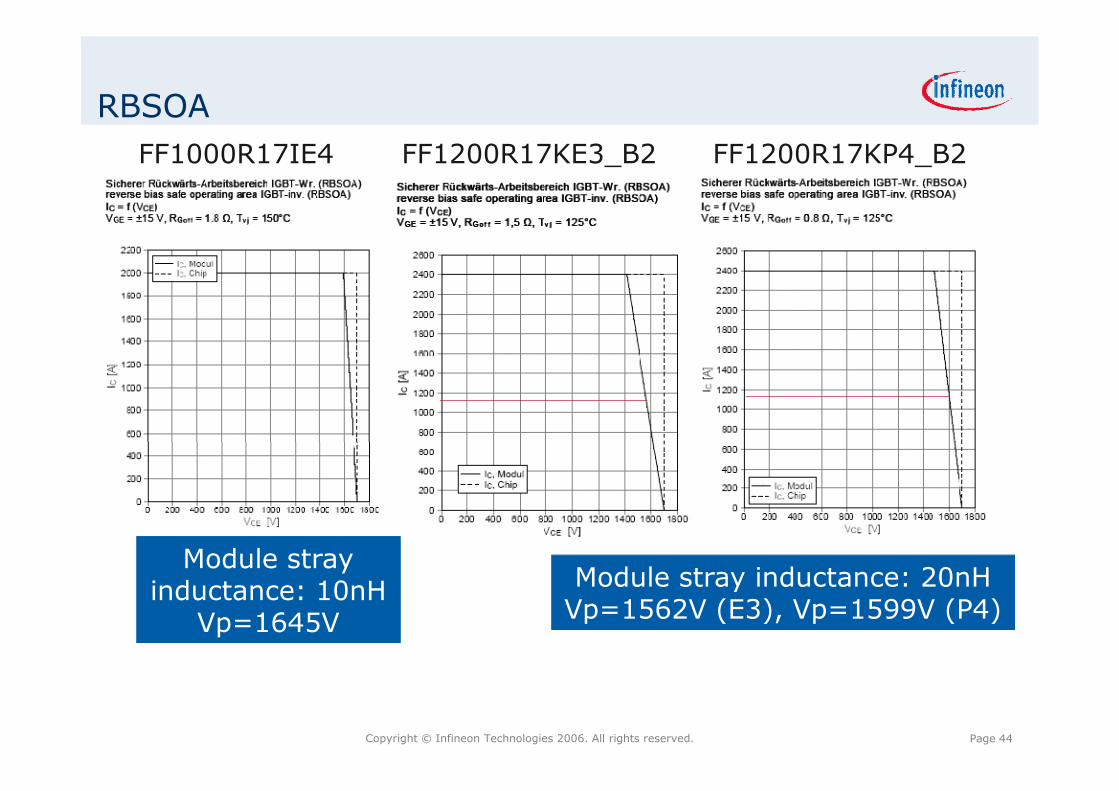
RBSOA
FF1000R17IE4 FF1200R17KE3_B2 FF1200R17KP4_B2
Module stray inductance: 20nHVp=1562V (E3), Vp=1599V (P4)
Module strayinductance: 10nH
Vp=1645V

Page 45Copyright © Infineon Technologies 2006. All rights reserved.
Output current – PP3 vs. IHM
Liquid
Air forced
PP3 Rthha per module=0.006k/W-> Max.Io=1150APP3 Rthha per module=0.024k/W- > Max. Io=610AIHM Rthha per module=0.008k/W-> Max. Io=800A
Page 46Copyright © Infineon Technologies 2006. All rights reserved.
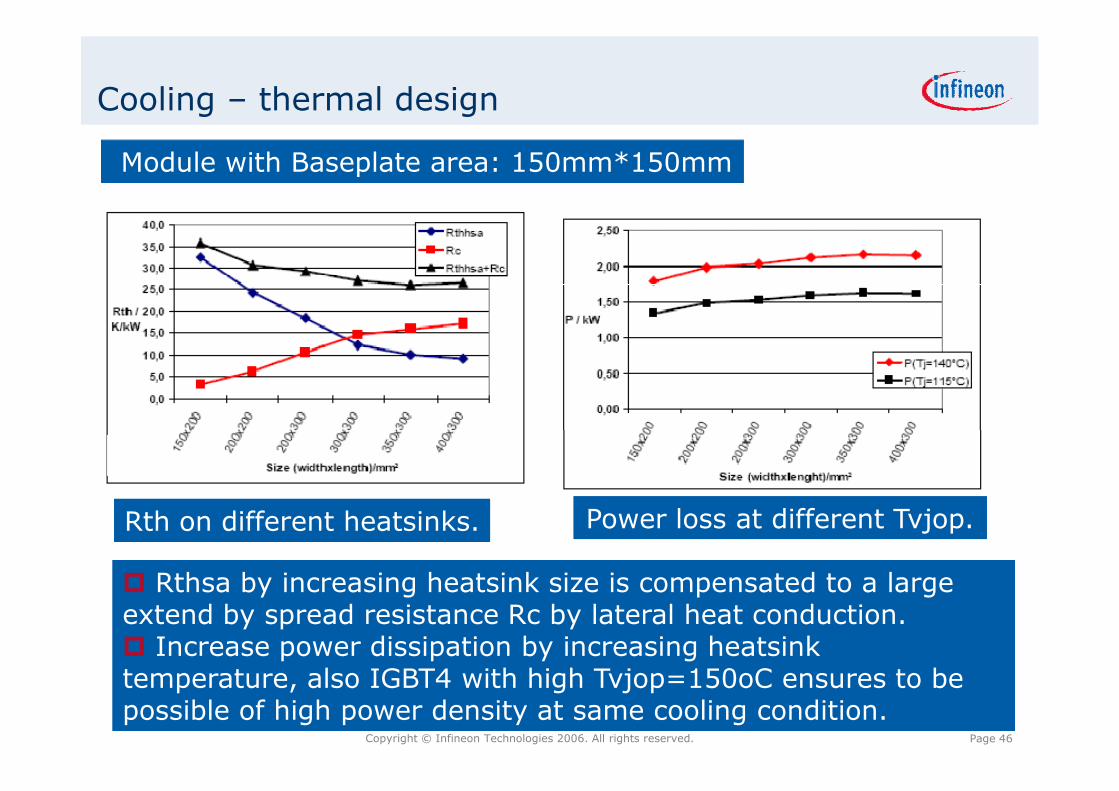
Cooling – thermal design
Module with Baseplate area: 150mm*150mm
Rth on different heatsinks. Power loss at different Tvjop.
Rthsa by increasing heatsink size is compensated to a largeextend by spread resistance Rc by lateral heat conduction. Increase power dissipation by increasing heatsinktemperature, also IGBT4 with high Tvjop=150oC ensures to bepossible of high power density at same cooling condition.

Page 47Copyright © Infineon Technologies 2006. All rights reserved.
Cooling - Air forced vs. heatpipe
Max. Ts=104.3oC- > Rthha =0.02K/W
Max. Ts=96.3oC-> Rthha = 0.0173K/W
Homogeneous heat spread
1.5MW DF,Max. Power losses=3.35kW (OL & margin)

Page 48Copyright © Infineon Technologies 2006. All rights reserved.
Cooling – Heatpipe vs. Liquid
Max. Ts=93.8oC- > Rthha =0.018K/W
Max. Ts=65oC-> Rthha = 0.012K/W
Page 49Copyright © Infineon Technologies 2006. All rights reserved.
Table of contents
High power density & IGBT module development
IGBT safe operational area & the design principle
Reliability requirement & estimation
High power density on CAV and wind power application

Page 50Copyright © Infineon Technologies 2006. All rights reserved.
Wear-out failures
Other failures (climatic stresses,chemical stresses)
End of Life: bond wire connections
End of Life: solder connections
Destruction of housing / terminals

Page 51Copyright © Infineon Technologies 2006. All rights reserved.
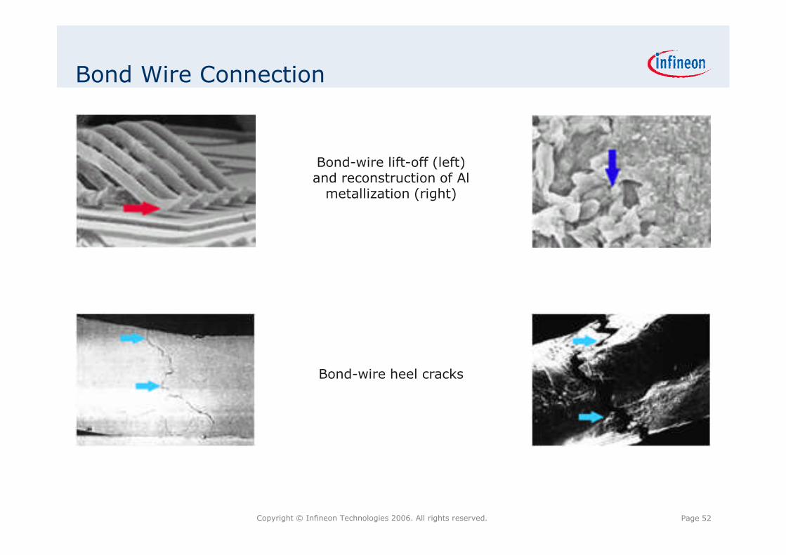
Bond wire connections
Degradation ofbond wire
connections:
Main influences
Application
No. of load cycles
Temperature delta of load cycles
Absolute temperature
Design & Manufacturing
Bond wire material
Bond wire loops
Chip metallization
Quality of the bond wire connection
The most important Test focussing on Wire Bond Connectionsis Power Cycling
Page 52Copyright © Infineon Technologies 2006. All rights reserved.
Bond Wire Connection
Bond-wire lift-off (left)and reconstruction of Al
metallization (right)
Bond-wire heel cracks

Page 53Copyright © Infineon Technologies 2006. All rights reserved.
Power Cycling
TChip
TDCB
TBaseplat
e
TCoole
r
Means driving the chip/bond wire system at two different junction temperatures.
Test Points (e.g.)Tj = 50K: TJ1 = 75C, TJ2 = 125C
Failure Criteria:An Increased Saturation Voltage of 5%

Page 54Copyright © Infineon Technologies 2006. All rights reserved.
Delamination
Delamination:
Main influences
Design & Manufacturing
Dimension of the components close to thesolder layers
Heat expansion coefficient and elasticityof the used materials
Composition of the solder
Thickness of the solder layers
Application
No. of load cycles
Temperature delta of the load cycles
Absolute temperature
Temperature gradient of the load cycles
The main important Tests focussing on Solder Connections arePower Cycling, Thermal Cycling and Thermal Shock Test

Page 55Copyright © Infineon Technologies 2006. All rights reserved.
Base plate and DCB material selection
Coefficient of thermal expansion (CTE)[ppm/K]
Thermal ShockTest Results
Page 56Copyright © Infineon Technologies 2006. All rights reserved.
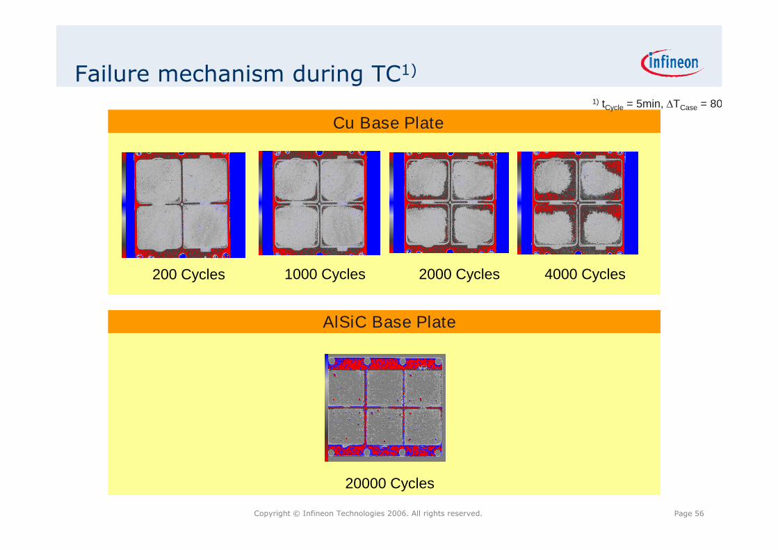
Failure mechanism during TC1)
200 Cycles 1000 Cycles 2000 Cycles 4000 Cycles
20000 Cycles
Cu Base Plate
AlSiC Base Plate
1) tCycle = 5min, TCase = 80K

Page 57Copyright © Infineon Technologies 2006. All rights reserved.
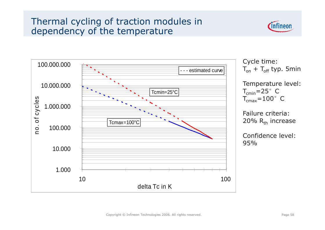
Thermal Cycling
Page 58Copyright © Infineon Technologies 2006. All rights reserved.
Cycle time:Ton + Toff typ. 5min
Temperature level:Tcmin=25°CTcmax=100°C
Failure criteria:20% Rth increase
Confidence level:95%
Thermal cycling of traction modules independency of the temperature
1.000
10.000
100.000
1.000.000
10.000.000
100.000.000
10 100delta Tc in K
no
.of
cy
cle
s
Tcmax=100°C
Tcmin=25°C
- - - estimated curve
Page 59Copyright © Infineon Technologies 2006. All rights reserved.
Reliability Test
Page 60Copyright © Infineon Technologies 2006. All rights reserved.
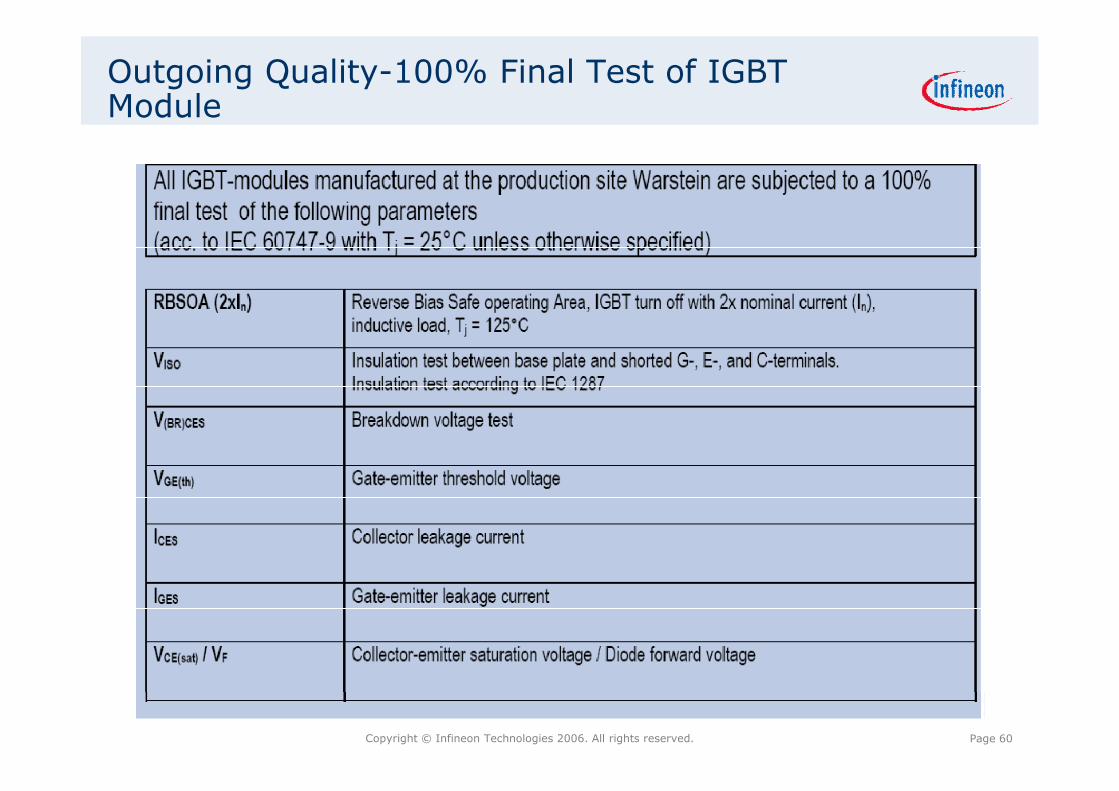
Outgoing Quality-100% Final Test of IGBTModule

Page 61Copyright © Infineon Technologies 2006. All rights reserved.
Table of contents
High power density & IGBT module development
IGBT safe operational area & the design principle
Reliability requirement & estimation
High power density on CAV and wind power application

Page 62Copyright © Infineon Technologies 2006. All rights reserved.
Wind power
Direct DriveDouble feed
IHM PrimePackTM EconoDualTM3 EconoPackTM+

Page 63Copyright © Infineon Technologies 2006. All rights reserved.
Mega–watt wind converter
Humidity, saltyHigh altitudeBare, remote
- Lifetime (PC/TC)- Reliability
- Maintenance - High power density- Compact- Flexible
- Cost-to-performance

Page 64Copyright © Infineon Technologies 2006. All rights reserved.
Requirement on wind converter
High switching frequency in grid side -> Low IGBT4 SW, even SiC High reliability and robustness - > IGBT4 modules Long expectation lifetime -> IGBT4 with high PC/TC, even next Easy to maintain -> phase module or modular power unit
Grid side
AC inductor,magnetic loop Inductor
Motor side
Page 65Copyright © Infineon Technologies 2006. All rights reserved.
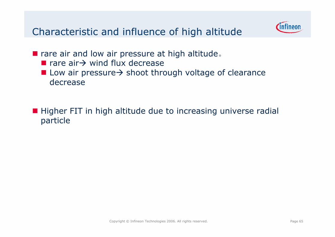
Characteristic and influence of high altitude
rare air and low air pressure at high altitude。 rare air wind flux decrease Low air pressure shoot through voltage of clearance
decrease
Higher FIT in high altitude due to increasing universe radialparticle

Page 66Copyright © Infineon Technologies 2006. All rights reserved.
Module clearance distance for high power solar
EconoDUAL3clearance distancebtw terminals is
10mm.
PrimePACKclearance distancebtw terminals is
19mm.

Page 67Copyright © Infineon Technologies 2006. All rights reserved.
IEC60664
According to Table F.1,270V OV Class:IV ->6KV impulse
Withstand voltage required
The severest condition:Pollutiondegree3, inhomogenous field,
Min.clearance distance of 5.5mm isrequired at 2000m altitude.

Page 68Copyright © Infineon Technologies 2006. All rights reserved.
Correction factor from IEC60664
4000m -> Factor: 1.29 ->Min. 7.1mm
6000m -> Factor: 1.70 ->Min. 9.35mm
The min. clearance distance of 9.35mm at high altitude of 6km is required.Therefore, the clearance of PrimePACK and EconoDUAL3 can meet the
requirement of high altitude application.

Page 69Copyright © Infineon Technologies 2006. All rights reserved.
IGBT modules ->Double Feed Wind System
WindPower
IGBT Module Rotor side Paralleling/ per arm
Grid side Paralleling/Per arm
Cooling
1.25MW EconoDUAL3 FF450R17ME4 2pcs FF450R17ME4FS450R17ME4
NN
Water
PrimePACK2/3 FF1000R17IE4 N FF650R17IE4 N Water
1.5MW EconoDUAL3 FF450R17ME4 3pcs FF450R17ME4 3pcs Water
PrimePACK2/3 FF1000R17IE4 2pcs FF650R17IE4 2pcs Air-forced
IHM BIHM A
FZ1600R17HP4FZ1600R17KE3
N FZ1600R17HP4FZ1600R17KE3
N Air-forced
2.0MW PrimePACK3 FF1000R17IE4 3pcs2pcs
FF1000R17IE4 2pcs2pcs
Air-forcedWater
IHM B FZ2400R17HP4 N FZ1600R17HP4 N Air-forced
EconoDUAL3 FF450R17ME4 4pcs FF450R17ME4 4pcs Water
*Remark:1) The proposal is based on the simulation conditions below as well as the general case experiences.
Vdc=1100V, Vin=690V, fo=0~15Hz, fs=2kHz @ rotor side, fo=50Hz, fs=3kHz @ grid side, OL=120%.2) The usage of the different IGBT solutions are mostly influenced by the real cooling system. Therefore, the
disclaimer rule should be complied.

Page 70Copyright © Infineon Technologies 2006. All rights reserved.
IGBT modules ->Full Power Wind System
WindPower
IGBT Module Rotor side Paralleling/per arm
Grid side Paralleling/Per arm
Cooling
1.5MW PrimePACK3 FF1000R17IE4 3pcs FF1000R17IE4 3pcs Water
IHM A FF1200R17KE3 2pcs FF1200R17KE3 2pcs Water
2.0MW PrimePACK3 FF1000R17IE4 3pcs FF1000R17IE4 3pcs Water
IHM B FZ2400R17HP4_B29
2pcs FZ2400R17HP4_B29
2pcs Water

Page 71Copyright © Infineon Technologies 2006. All rights reserved.
CAV segmentsand the market we especially look at…
City bus
Refuse truck
Commercial
Loader
Bulldozer Excavator
Dump truck
Construction
Focus on propulsion andauxiliaries…
Harvester
Agriculture
Tractor
LCV
ForkliftTransport

Page 72Copyright © Infineon Technologies 2006. All rights reserved.
CAV products porfilio
Page 73Copyright © Infineon Technologies 2006. All rights reserved.
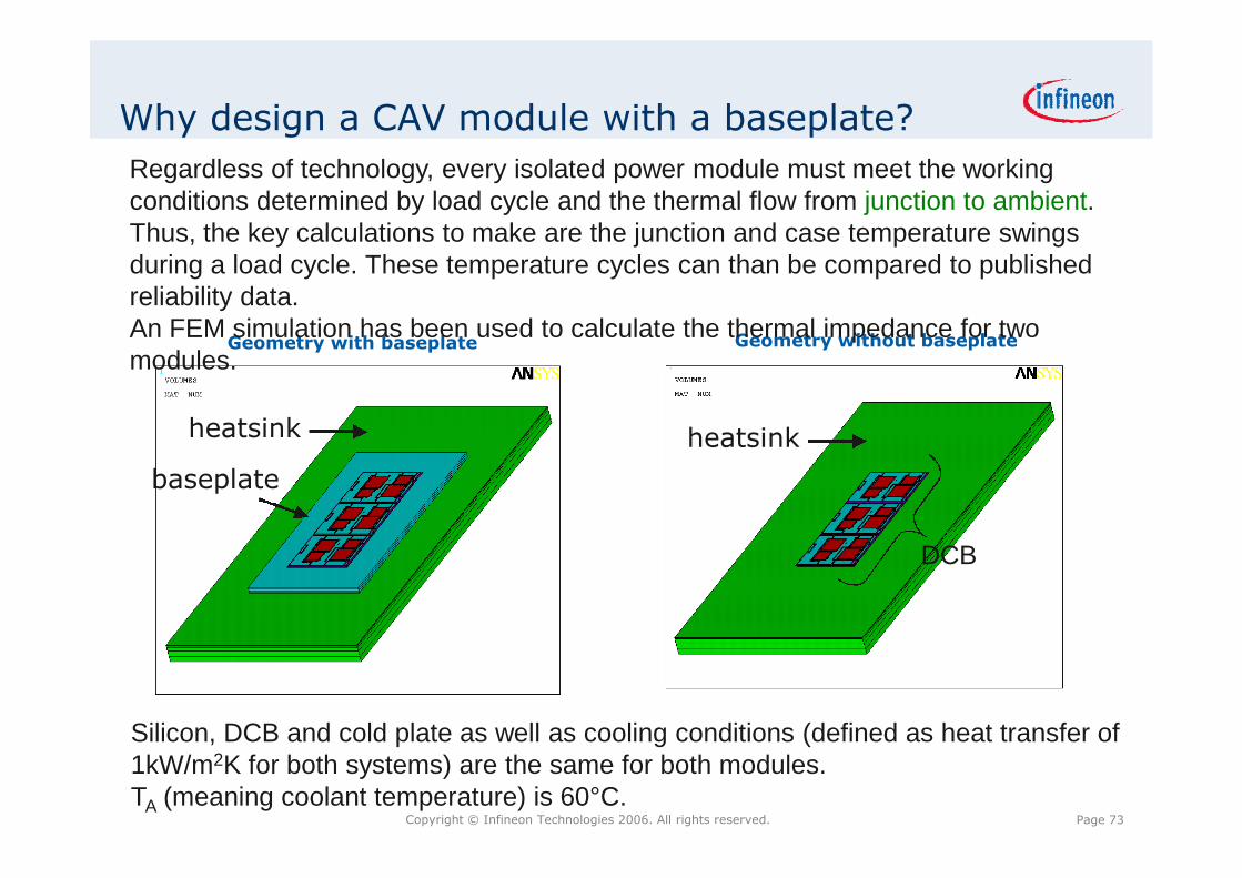
Why design a CAV module with a baseplate?
heatsink heatsink
baseplate
DCB
Geometry with baseplate Geometry without baseplate
Regardless of technology, every isolated power module must meet the workingconditions determined by load cycle and the thermal flow from junction to ambient.Thus, the key calculations to make are the junction and case temperature swingsduring a load cycle. These temperature cycles can than be compared to publishedreliability data.An FEM simulation has been used to calculate the thermal impedance for twomodules.
Silicon, DCB and cold plate as well as cooling conditions (defined as heat transfer of1kW/m2K for both systems) are the same for both modules.TA (meaning coolant temperature) is 60°C.

Page 74Copyright © Infineon Technologies 2006. All rights reserved.
Why design a CAV module with a baseplate?The thermal stack up
soldercopper
Al2O3
75µm of thermal grease l=1 W/mK
10mm aluminum heatsink
soldercopper
silicon die
copper baseplate
Al2O3
silicon diesolder
copper
copper75µm of thermal grease l=1 W/mK
10mm aluminum heatsink
Geometry with baseplate
Geometry without baseplate
Active area 2
Active area 1
PIGBT=145W
PIGBT=100W
Active area 2
Active area 1
Baseplate enlarges active area of heat flowfrom module to heatsink. For the sameTJ=125°C the module with a baseplate candissipate 45% more power. This results ineither more available inverter power orreduced junction temperatures.

Page 75Copyright © Infineon Technologies 2006. All rights reserved.
Why design a CAV module with a baseplate?Typical load profile (simulations)
High dynamic load cycles are shorterthan 5s
IGBT loses as result of applied load cycle
0
50
100
150
200
0 5 10 15 20 25 30
Time [s]
Lo
ss
es
[W]
P_IGBT
1
2
3
4 5
1
Source: Infineon SystemEngineering
IGBT losses as a result of applied load cycles

Page 76Copyright © Infineon Technologies 2006. All rights reserved.
Why design a CAV module with a baseplate?Typical load profile – influence on lifetime (simulations)
with Base...without B...
0 30.005.00 10.00 15.00 20.00 25.00
60.00
80.00
65.00
70.00
75.00
t [s]
T [°C]
with BPwithout ...
0 30.005.00 10.00 15.00 20.00 25.00
50.0
110.0
62.5
75.0
87.5
100.0
Tj [°C]
t [s]
withbaseplate
withoutbaseplate
IGBT Junction Temperature Solder and case temperature
withbaseplate
withoutbaseplate
∆T=19°C∆T=8°C
Benefits of a module with baseplate vs. module w/o a baseplate for a givenapplication:-reduced junction temperature by 19°C results in an extra 19e6 power cycles-reduced case temperature by 8°C results in available TC of >> 500 000 cyclesResult: longer lifetimes or same lifetime with a lower current rated moduleand /or increased inverter ratings.
Page 77Copyright © Infineon Technologies 2006. All rights reserved.
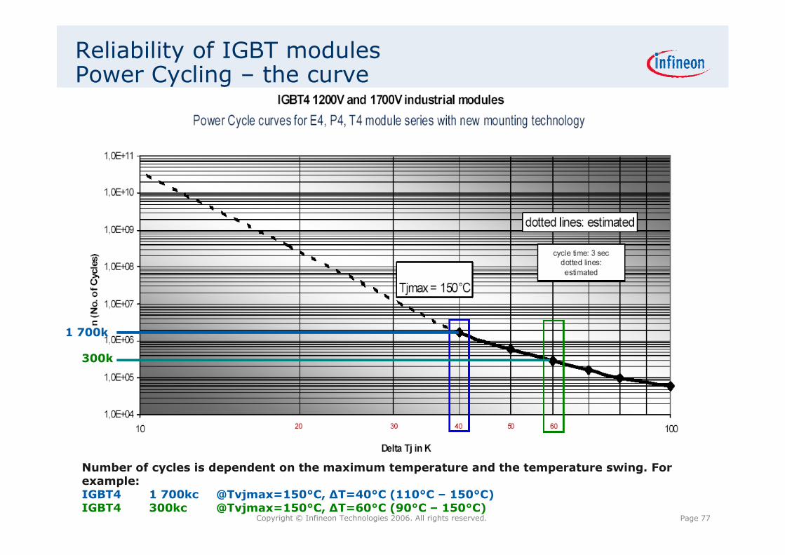
Reliability of IGBT modulesPower Cycling – the curve
Number of cycles is dependent on the maximum temperature and the temperature swing. Forexample:IGBT4 1 700kc @Tvjmax=150°C, ∆T=40°C (110°C – 150°C)IGBT4 300kc @Tvjmax=150°C, ∆T=60°C (90°C – 150°C)
1 700k
300k

Page 78Copyright © Infineon Technologies 2006. All rights reserved.
Active thermal cycling:12.000 cycles @T=80°C are standard

Page 79Copyright © Infineon Technologies 2006. All rights reserved.
EconoDUAL™3 for highest thermal loads -more thermal cycling capability is possible
Standard EconoDUAL™3after 10.000 cycles (T=80°C)
„CAV“ EconoDUAL™3 test deviceafter 10.000 cycles (T=80°C)
clear delamination, below chip
EoL: 5.000 (guaranteed)
minimal delamination
EoL >> 10.000 cycles
substrate soldering layer substrate soldering layer
chip soldering layer chip soldering layer
Page 80Copyright © Infineon Technologies 2006. All rights reserved.
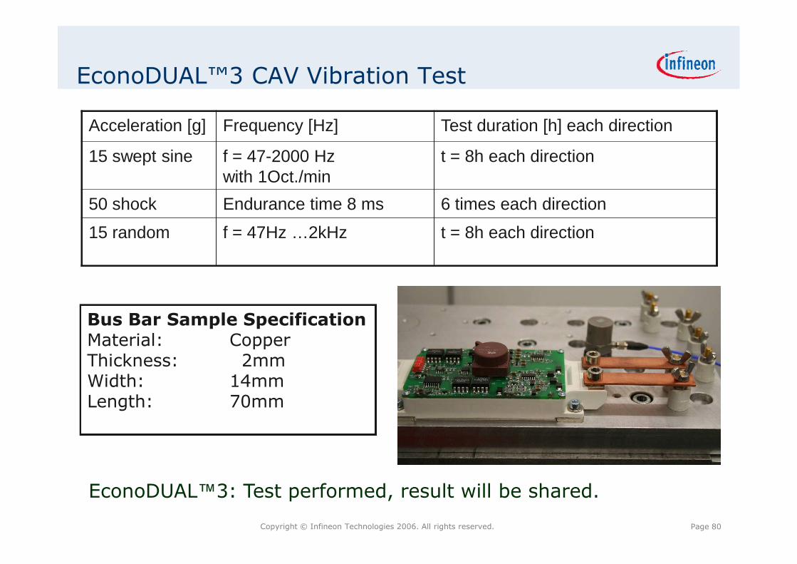
EconoDUAL™3 CAV Vibration Test
Acceleration [g] Frequency [Hz] Test duration [h] each direction
15 swept sine f = 47-2000 Hzwith 1Oct./min
t = 8h each direction
50 shock Endurance time 8 ms 6 times each direction
15 random f = 47Hz …2kHz t = 8h each direction
EconoDUAL™3: Test performed, result will be shared.
Bus Bar Sample SpecificationMaterial: CopperThickness: 2mmWidth: 14mmLength: 70mm

Infineon –Never stop thinking