Embed Size (px)
Citation preview
REV. A
Information furnished by Analog Devices is believed to be accurate andreliable. However, no responsibility is assumed by Analog Devices for itsuse, nor for any infringements of patents or other rights of third parties thatmay result from its use. No license is granted by implication or otherwiseunder any patent or patent rights of Analog Devices. Trademarks andregistered trademarks are the property of their respective companies.
One Technology Way, P.O. Box 9106, Norwood, MA 02062-9106, U.S.A.
Tel: 781/329-4700 www.analog.com
Fax: 781/326-8703 © 2003 Analog Devices, Inc. All rights reserved.
AD9874*
IF Digitizing Subsystem
*Protected by U.S. Patent No. 5,969,657;
FEATURES
10 MHz to 300 MHz Input Frequency
7.2 kHz to 270 kHz Output Signal Bandwidth
8.1 dB SSB NF
0 dBm IIP3
AGC Free Range up to –34 dBm
12 dB Continuous AGC Range
16 dB Front End Attenuator
Baseband I/Q 16-Bit (or 24-Bit) Serial Digital Output
LO and Sampling Clock Synthesizers
Programmable Decimation Factor, Output Format,
AGC, and Synthesizer Settings
370 Input Impedance
2.7 V to 3.6 V Supply Voltage
Low Current Consumption: 20 mA
48-Lead LQFP Package (1.4 mm Thick)
APPLICATIONS
Multimode Narrow-Band Radio Products
Analog/Digital UHF/VHF FDMA Receivers
TETRA, APCO25, GSM/EDGE
Portable and Mobile Radio Products
Base Station Applications
SATCOM Terminals
- ADCLNA
DAC AGC
VOLTAGEREFERENCE
SPI
CONTROL LOGIC
FORMATTING/SSIDECIMATIONFILTER
LOSYN CLK SYN
LO VCO ANDLOOP FILTER
IFIN
FREF
DOUTA
DOUTB
FS
CLKOUT
SYNCBPEPDPCVREFNVCMVREFP
MXOP MXON IF2P IF2N GCP GCN
–16dB
AD9874
CLKNCLKPIOUTCLONLOPIOUTL
LOOP FILTER
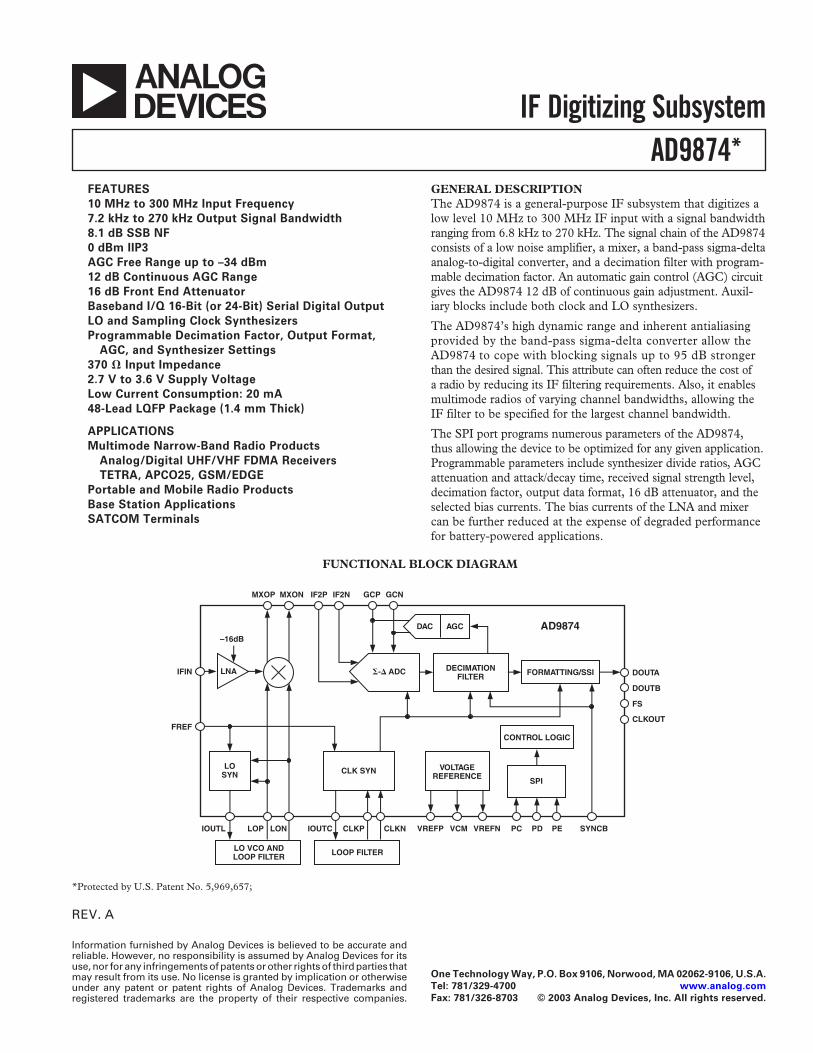
GENERAL DESCRIPTIONThe AD9874 is a general-purpose IF subsystem that digitizes alow level 10 MHz to 300 MHz IF input with a signal bandwidthranging from 6.8 kHz to 270 kHz. The signal chain of the AD9874consists of a low noise amplifier, a mixer, a band-pass sigma-deltaanalog-to-digital converter, and a decimation filter with program-mable decimation factor. An automatic gain control (AGC) circuitgives the AD9874 12 dB of continuous gain adjustment. Auxil-iary blocks include both clock and LO synthesizers.
The AD9874’s high dynamic range and inherent antialiasingprovided by the band-pass sigma-delta converter allow theAD9874 to cope with blocking signals up to 95 dB strongerthan the desired signal. This attribute can often reduce the cost ofa radio by reducing its IF filtering requirements. Also, it enablesmultimode radios of varying channel bandwidths, allowing theIF filter to be specified for the largest channel bandwidth.
The SPI port programs numerous parameters of the AD9874,thus allowing the device to be optimized for any given application.Programmable parameters include synthesizer divide ratios, AGCattenuation and attack/decay time, received signal strength level,decimation factor, output data format, 16 dB attenuator, and theselected bias currents. The bias currents of the LNA and mixercan be further reduced at the expense of degraded performancefor battery-powered applications.
FUNCTIONAL BLOCK DIAGRAM
REV. A
AD9874
–2–
TABLE OF CONTENTS
AD9874—SPECIFICATIONS . . . . . . . . . . . . . . . . . . . . . . . 3ABSOLUTE MAXIMUM RATINGS . . . . . . . . . . . . . . . . . 5PIN CONFIGURATION/DESCRIPTION . . . . . . . . . . . . . 6DEFINITION OF SPECIFICATIONS/
TEST METHODS . . . . . . . . . . . . . . . . . . . . . . . . . . . . . . 7TYPICAL PERFORMANCE CHARACTERISTICS . . . . . 8SERIAL PERIPHERAL INTERFACE (SPI) . . . . . . . . . . . 13SYNCHRONOUS SERIAL INTERFACE (SSI) . . . . . . . . 16
Synchronization Using SYNCB . . . . . . . . . . . . . . . . . . . . 18Interfacing to DSPs . . . . . . . . . . . . . . . . . . . . . . . . . . . . . 18
POWER CONTROL . . . . . . . . . . . . . . . . . . . . . . . . . . . . . 19LO SYNTHESIZER . . . . . . . . . . . . . . . . . . . . . . . . . . . . . . 19
Fast Acquire Mode . . . . . . . . . . . . . . . . . . . . . . . . . . . . . 20CLOCK SYNTHESIZER . . . . . . . . . . . . . . . . . . . . . . . . . . 21IF LNA/MIXER . . . . . . . . . . . . . . . . . . . . . . . . . . . . . . . . . 22BAND-PASS SIGMA DELTA (-) ADC . . . . . . . . . . . . 24DECIMATION FILTER . . . . . . . . . . . . . . . . . . . . . . . . . . 26VARIABLE GAIN AMPLIFIER WITH AGC . . . . . . . . . . 28
Variable Gain Control . . . . . . . . . . . . . . . . . . . . . . . . . . . 28Automatic Gain Control . . . . . . . . . . . . . . . . . . . . . . . . . 29System NF vs. VGA Control . . . . . . . . . . . . . . . . . . . . . . 31
APPLICATION CONSIDERATIONS . . . . . . . . . . . . . . . 32Frequency Planning . . . . . . . . . . . . . . . . . . . . . . . . . . . . . 32Spurious Responses . . . . . . . . . . . . . . . . . . . . . . . . . . . . . 33
EXTERNAL PASSIVE COMPONENTREQUIREMENTS . . . . . . . . . . . . . . . . . . . . . . . . . . . . . 34
APPLICATIONS . . . . . . . . . . . . . . . . . . . . . . . . . . . . . . . . 34Superheterodyne Receiver . . . . . . . . . . . . . . . . . . . . . . . . 34Synchronization of Multiple AD9874s . . . . . . . . . . . . . . . 36Split Path Rx Architecture . . . . . . . . . . . . . . . . . . . . . . . . 37Hung Mixer Mode . . . . . . . . . . . . . . . . . . . . . . . . . . . . . . 38
LAYOUT EXAMPLEEVALUATION BOARD AND SOFTWARE . . . . . . . . . 38
OUTLINE DIMENSIONS . . . . . . . . . . . . . . . . . . . . . . . . . 39REVISION HISTORY . . . . . . . . . . . . . . . . . . . . . . . . . . . . 40
REV. A
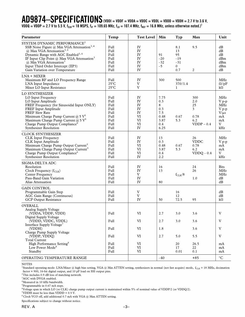
AD9874–SPECIFICATIONS
–3–
Parameter Temp Test Level Min Typ Max Unit
SYSTEM DYNAMIC PERFORMANCE2
SSB Noise Figure @ Min VGA Attenuation3, 4 Full IV 8.1 9.5 dB @ Max VGA Attenuation3, 4 Full IV 13 dBDynamic Range with AGC Enabled3, 4 Full IV 91 95 dBIF Input Clip Point @ Max VGA Attenuation3 Full IV –20 –19 dBm @ Min VGA Attenuation3 Full IV –32 –31 dBmInput Third Order Intercept (IIP3) Full IV –5 0 dBmGain Variation over Temperature Full IV 0.7 2 dB
LNA + MIXERMaximum RF and LO Frequency Range Full IV 300 500 MHzLNA Input Impedance 25oC V 370//1.4 //pFMixer LO Input Resistance 25oC V 1 k
LO SYNTHESIZERLO Input Frequency Full IV 7.75 300 MHzLO Input Amplitude Full IV 0.3 2.0 V p-pFREF Frequency (for Sinusoidal Input ONLY) Full IV 8 25 MHzFREF Input Amplitude Full IV 0.3 3 V p-pFREF Slew Rate Full IV 7.5 V/sMinimum Charge Pump Current @ 5 V5 Full VI 0.48 0.67 0.78 mAMaximum Charge Pump Current @ 5 V5 Full VI 3.87 5.3 6.2 mACharge Pump Output Compliance6 Full VI 0.4 VDDP – 0.4 VSynthesizer Resolution Full IV 6.25 kHz
CLOCK SYNTHESIZERCLK Input Frequency Full IV 13 26 MHzCLK Input Amplitude Full IV 0.3 VDDC V p-pMinimum Charge Pump Output Current5 Full VI 0.48 0.67 0.78 mAMaximum Charge Pump Output Current5 Full VI 3.87 5.3 6.2 mACharge Pump Output Compliance6 Full VI 0.4 VDDQ – 0.4 VSynthesizer Resolution Full IV 2.2 kHz
SIGMA-DELTA ADCResolution Full IV 16 24 BitsClock Frequency (fCLK) Full IV 13 26 MHzCenter Frequency Full V fCLK/8 MHzPass-Band Gain Variation Full IV 1.0 dBAlias Attenuation Full IV 80 dB
GAIN CONTROLProgrammable Gain Step Full V 16 dBAGC Gain Range (Continuous) Full V 12 dBGCP Output Resistance Full IV 50 72.5 95 k
OVERALLAnalog Supply Voltage
(VDDA, VDDF, VDDI) Full VI 2.7 3.0 3.6 VDigital Supply Voltage
(VDDD, VDDC, VDDL) Full VI 2.7 3.0 3.6 VInterface Supply Voltage7
(VDDH) Full VI 1.8 3.6 VCharge Pump Supply Voltage
(VDDP, VDDQ) Full VI 2.7 5.0 5.5 VTotal Current
High Performance Setting8 Full VI 20 26.5 mALow Power Mode8 Full VI 17 22 mAStandby Full VI 0.01 0.1 mA
OPERATING TEMPERATURE RANGE –40 +85 °CNOTES1Standard operating mode: LNA/Mixer @ high bias setting, VGA @ Min ATTEN setting, synthesizers in normal (not fast acquire) mode, fCLK = 18 MHz, decimationfactor = 900, 16-bit digital output, and 10 pF load on SSI output pins.
2This includes 0.9 dB loss of matching network.3AGC with DVGA enabled.4Measured in 10 kHz bandwidth.5Programmable in 0.67 mA steps.6Voltage span in which LO (or CLK) charge pump output current is maintained within 5% of nominal value of VDDP/2 (or VDDQ/2).7VDDH must be less than VDDD + 0.5 V.8 Clock VCO off, add additional 0.7 mA with VGA @ Max ATTEN setting.
Specifications subject to change without notice.
(VDDI = VDDF = VDDA = VDDC = VDDL = VDDD = VDDH = 2.7 V to 3.6 V,VDDQ = VDDP = 2.7 V to 5.5 V, fCLK = 18 MSPS, fIF = 109.65 MHz, fLO = 107.4 MHz, fREF = 16.8 MHz, unless otherwise noted.)1
REV. A
AD9874
–4–
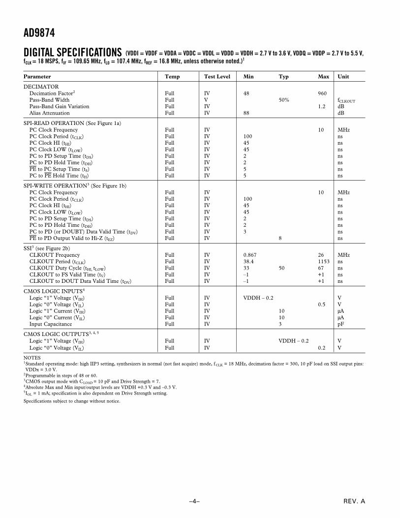
DIGITAL SPECIFICATIONS (VDDI = VDDF = VDDA = VDDC = VDDL = VDDD = VDDH = 2.7 V to 3.6 V, VDDQ = VDDP = 2.7 V to 5.5 V,fCLK = 18 MSPS, fIF = 109.65 MHz, fLO = 107.4 MHz, fREF = 16.8 MHz, unless otherwise noted.)1
Parameter Temp Test Level Min Typ Max Unit
DECIMATORDecimation Factor2 Full IV 48 960Pass-Band Width Full V 50% fCLKOUT
Pass-Band Gain Variation Full IV 1.2 dBAlias Attenuation Full IV 88 dB
SPI-READ OPERATION (See Figure 1a)PC Clock Frequency Full IV 10 MHzPC Clock Period (tCLK) Full IV 100 nsPC Clock HI (tHI) Full IV 45 nsPC Clock LOW (tLOW) Full IV 45 nsPC to PD Setup Time (tDS) Full IV 2 nsPC to PD Hold Time (tDH) Full IV 2 nsPE to PC Setup Time (tS) Full IV 5 nsPC to PE Hold Time (tH) Full IV 5 ns
SPI-WRITE OPERATION3 (See Figure 1b)PC Clock Frequency Full IV 10 MHzPC Clock Period (tCLK) Full IV 100 nsPC Clock HI (tHI) Full IV 45 nsPC Clock LOW (tLOW) Full IV 45 nsPC to PD Setup Time (tDS) Full IV 2 nsPC to PD Hold Time (tDH) Full IV 2 nsPC to PD (or DOUBT) Data Valid Time (tDV) Full IV 3 nsPE to PD Output Valid to Hi-Z (tEZ) Full IV 8 ns
SSI3 (see Figure 2b)CLKOUT Frequency Full IV 0.867 26 MHzCLKOUT Period (tCLK) Full IV 38.4 1153 nsCLKOUT Duty Cycle (tHI, tLOW) Full IV 33 50 67 nsCLKOUT to FS Valid Time (tV) Full IV –1 +1 nsCLKOUT to DOUT Data Valid Time (tDV) Full IV –1 +1 ns
CMOS LOGIC INPUTS4
Logic “1” Voltage (VIH) Full IV VDDH – 0.2 VLogic “0” Voltage (VIL) Full IV 0.5 VLogic “1” Current (VIH) Full IV 10 µALogic “0” Current (VIL) Full IV 10 µAInput Capacitance Full IV 3 pF
CMOS LOGIC OUTPUTS3, 4, 5
Logic “1” Voltage (VIH) Full IV VDDH – 0.2 VLogic “0” Voltage (VIL) Full IV 0.2 V
NOTES1Standard operating mode: high IIP3 setting, synthesizers in normal (not fast acquire) mode, f CLK = 18 MHz, decimation factor = 300, 10 pF load on SSI output pins:VDDx = 3.0 V.
2Programmable in steps of 48 or 60.3CMOS output mode with CLOAD = 10 pF and Drive Strength = 7.4Absolute Max and Min input/output levels are VDDH +0.3 V and –0.3 V.5IOL = 1 mA; specification is also dependent on Drive Strength setting.
Specifications subject to change without notice.
REV. A
AD9874
–5–
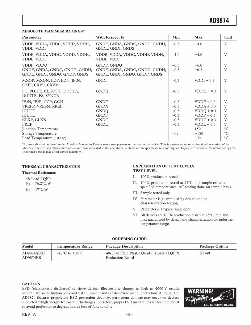
CAUTIONESD (electrostatic discharge) sensitive device. Electrostatic charges as high as 4000 V readilyaccumulate on the human body and test equipment and can discharge without detection. Although theAD9874 features proprietary ESD protection circuitry, permanent damage may occur on devicessubjected to high energy electrostatic discharges. Therefore, proper ESD precautions are recommendedto avoid performance degradation or loss of functionality.
ABSOLUTE MAXIMUM RATINGS*
Parameter With Respect to Min Max Unit
VDDF, VDDA, VDDC, VDDD, VDDH, GNDF, GNDA, GNDC, GNDD, GNDH, –0.3 +4.0 VVDDL, VDDI GNDL, GNDI, GNDS
VDDF, VDDA, VDDC, VDDD, VDDH, VDDR, VDDA, VDDC, VDDD, VDDH, –4.0 +4.0 VVDDL, VDDI VDDL, VDDI
VDDP, VDDQ GNDP, GNDQ –0.3 +6.0 VGNDF, GNDA, GNDC, GNDD, GNDH, GNDF, GNDA, GNDC, GNDD, GNDH, –0.3 +0.3 VGNDL, GNDI, GNDQ, GNDP, GNDS GNDL, GNDI, GNDQ, GNDP, GNDS
MXOP, MXON, LOP, LON, IFIN, GNDI –0.3 VDDI + 0.3 VCXIF, CXVL, CXVM
PC, PD, PE, CLKOUT, DOUTA, GNDH –0.3 VDDH + 0.3 VDOUTB, FS, SYNCB
IF2N, IF2P, GCP, GCN GNDF –0.3 VDDF + 0.3 VVREFP, VREFN, RREF GNDA –0.3 VDDA + 0.3 VIOUTC GNDQ –0.3 VDDQ + 0.3 VIOUTL GNDP –0.3 VDDP + 0.3 VCLKP, CLKN GNDC –0.3 VDDC + 0.3 VFREF GNDL –0.3 VDDL + 0.3 VJunction Temperature 150 °CStorage Temperature –65 +150 °CLead Temperature (10 sec) 300 °C*Stresses above those listed under Absolute Maximum Ratings may cause permanent damage to the device. This is a stress rating only; functional operation of thedevice at these or any other conditions above those indicated in the operational sections of this specification is not implied. Exposure to absolute maximum ratings forextended periods may affect device reliability.
ORDERING GUIDE
Model Temperature Range Package Description Package Option
AD9874ABST –40°C to +85°C 48-Lead Thin Plastic Quad Flatpack (LQFP) ST-48AD9874EB Evaluation Board
EXPLANATION OF TEST LEVELSTEST LEVEL
I. 100% production tested.
II. 100% production tested at 25°C and sample tested atspecified temperatures. AC testing done on sample basis.
III. Sample tested only.
IV. Parameter is guaranteed by design and/orcharacterization testing.
V. Parameter is a typical value only.
VI. All devices are 100% production tested at 25°C; min andmax guaranteed by design and characterization for industrialtemperature range.
THERMAL CHARACTERISTICS
Thermal Resistance
48-Lead LQFPJA = 76.2°C/W
JC = 17°C/W
REV. A
AD9874
–6–
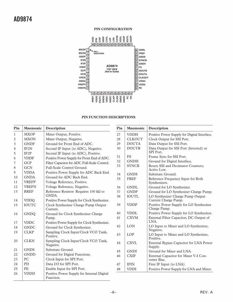
PIN CONFIGURATION
36
35
34
33
32
31
30
29
28
27
26
25
1
2
3
4
5
6
7
8
9
10
11
12
48 47 46 45 44 39 38 3743
PIN 1IDENTIFIER
TOP VIEW(Not to Scale)
GNDL
FREF
GNDS
SYNCB
GNDH
FS
DOUTB
MXOP
MXON
GNDF
IF2N
IF2P
VDDF
GCP
GCN
VDDA
GNDA
VREFP
DOUTA
CLKOUT
VDDH
VDDD
AD9874
VREFN PE
VD
DI
IFIN
CX
IF
GN
DI
CX
VL
LO
P
LO
N
CX
VM
VD
DL
VD
DP
IOU
TL
GN
DP
RR
EF
VD
DQ
IOU
TC
GN
DQ
VD
DC
GN
DC
CL
KP
CL
KN
GN
DS
GN
DD
PC
PD
404142
13 191817161514 20 21 22 23 24
PIN FUNCTION DESCRIPTIONS
Pin Mnemonic Description
1 MXOP Mixer Output, Positive.2 MXON Mixer Output, Negative.3 GNDF Ground for Front End of ADC.4 IF2N Second IF Input (to ADC), Negative.5 IF2P Second IF Input (to ADC), Positive.6 VDDF Positive Power Supply for Front End of ADC.7 GCP Filter Capacitor for ADC Full-Scale Control.8 GCN Full-Scale Control Ground.9 VDDA Positive Power Supply for ADC Back End.10 GNDA Ground for ADC Back End.11 VREFP Voltage Reference, Positive.12 VREFN Voltage Reference, Negative.13 RREF Reference Resistor: Requires 100 kΩ to
GNDA.14 VDDQ Positive Power Supply for Clock Synthesizer.15 IOUTC Clock Synthesizer Charge Pump Output
Current.16 GNDQ Ground for Clock Synthesizer Charge
Pump.17 VDDC Positive Power Supply for Clock Synthesizer.18 GNDC Ground for Clock Synthesizer.19 CLKP Sampling Clock Input/Clock VCO Tank,
Positive.20 CLKN Sampling Clock Input/Clock VCO Tank,
Negative.21 GNDS Substrate Ground.22 GNDD Ground for Digital Functions.23 PC Clock Input for SPI Port.24 PD Data I/O for SPI Port.25 PE Enable Input for SPI Port.26 VDDD Positive Power Supply for Internal Digital
Function.
27 VDDH Positive Power Supply for Digital Interface.28 CLKOUT Clock Output for SSI Port.29 DOUTA Data Output for SSI Port.30 DOUTB Data Output for SSI Port (Inverted) or
SPI Port.31 FS Frame Sync for SSI Port.32 GNDH Ground for Digital Interface.33 SYNCB Resets SSI and Decimator Counters;
Active Low.34 GNDS Substrate Ground.35 FREF Reference Frequency Input for Both
Synthesizers.36 GNDL Ground for LO Synthesizer.37 GNDP Ground for LO Synthesizer Charge Pump.38 IOUTL LO Synthesizer Charge Pump Output
Current Charge Pump.39 VDDP Positive Power Supply for LO Synthesizer
Charge Pump.40 VDDL Positive Power Supply for LO Synthesizer.41 CXVM External Filter Capacitor; DC Output of
LNA.42 LON LO Input to Mixer and LO Synthesizer,
Negative.43 LOP LO Input to Mixer and LO Synthesizer,
Positive.44 CXVL External Bypass Capacitor for LNA Power
Supply.45 GNDI Ground for Mixer and LNA.46 CXIF External Capacitor for Mixer V-I Con-
verter Bias.47 IFIN First IF Input (to LNA).48 VDDI Positive Power Supply for LNA and Mixer.
Pin Mnemonic Description
REV. A
AD9874
–7–
DEFINITION OF SPECIFICATIONS/TEST METHODS
Single-Sideband Noise Figure (SSB NF)Noise figure (NF) is defined as the degradation in SNR perfor-mance (in dB) of an IF input signal after it passes through acomponent or system. It can be expressed with the equation
Noise Figure SNR SNRIN OUT= ×10 log( )
The term SSB is applicable for heterodyne systems containing amixer. It indicates that the desired signal spectrum resides ononly one side of the LO frequency (i.e., single sideband); thus a“noiseless” mixer has a noise figure of 3 dB.
The AD9874’s SSB noise figure is determined by the equation
SSB NF P BW dBm Hz SNRIN= − × ( ) − −10 174log
where PIN is the input power of an unmodulated carrier, BW isthe noise measurement bandwidth, –174 dBm/Hz is the thermalnoise floor at 293 K, and SNR is the measured signal-to-noiseratio in dB of the AD9874.
Note that PIN is set to –85 dBm to minimize any degradation inmeasured SNR due to phase noise from the RF and LO signalgenerators. The IF frequency, CLK frequency, and decimationfactors are selected to minimize any spurious componentsfalling within the measurement bandwidth. Note also that abandwidth of 10 kHz is used for the data sheet specification.Refer to Figures 22a and 22b for an indication of how NF varieswith BW. Also, refer to the TPCs to see how NF is affected bydifferent operating conditions. All references to noise figureswithin this data sheet imply single-sideband noise figure.
Input Third Order Intercept (IIP3)IIP3 is a figure of merit used to determine a component’s orsystem’s susceptibility to intermodulation distortion (IMD)from its third order nonlinearities. Two unmodulated carriers ata specified frequency relationship (f1 and f2) are injected into anonlinear system exhibiting third order nonlinearities producingIMD components at 2f1 – f2 and 2f2 – f1. IIP3 graphically repre-sents the extrapolated intersection of the carrier’s input powerwith the third order IMD component when plotted in dB. Thedifference in power (D in dBc) between the two carriers and theresulting third order IMD components can be determined fromthe equation
D IIP PIN= ×2 3( – )
Dynamic Range (DR)Dynamic range is the measure of a small target input signal(PTARGET) in the presence of a large unwanted interferer signal(PINTER). Typically, the large signal will cause some unwantedcharacteristic of the component or system to degrade, thusmaking it unable to detect the smaller target signal correctly. Inthe case of the AD9874, it is often a degradation in noise figureat increased VGA attenuation settings that limits its dynamicrange (refer to TPCs 15a, 15b, and 15c).
The test method for the AD9874 is as follows. The small targetsignal (an unmodulated carrier) is input at the center of the IFfrequency, and its power level (PTARGET) is adjusted to achieve anSNRTARGET of 6 dB. The power of the signal is then increased by3 dB prior to injecting the interferer signal. The offset frequencyof the interferer signal is selected so that aliases produced bythe decimation filter’s response as well as phase noise from the LO(due to reciprocal mixing) do not fall back within the measurementbandwidth. For this reason, an offset of 110 kHz was selected.The interferer signal (also an unmodulated carrier) is theninjected into the input and its power level is increased to thepoint (PINTER) where the target signal SNR is reduced to 6 dB.The dynamic range is determined with the equation:
DR P P SNRINTER TARGET TARGET= +–
Note that the AD9874’s AGC is enabled for this test.
IF Input Clip PointThe IF input clip point is defined as 2 dB below the input powerlevel (PIN), resulting in the clipping of the AD9874’s ADC.Unlike other linear components that typically exhibit a softcompression (characterized by its 1 dB compression point), anADC exhibits a hard compression once its input signal exceedsits rated maximum input signal range. In the case of the AD9874,which contains a - ADC, hard compression should be avoidedbecause it causes severe SNR degradation.
REV. A
AD9874–Typical Performance Characteristics
–8–
NOISE FIGURE – dB
PE
RC
EN
TAG
E –
%
100
7.2 7.5 7.8 8.1 8.4 8.7 9.0
80
60
40
20
0
–40C +25C +85C
TPC 1a. CDF of SSB Noise Figure(VDDx = 3.0 V, High Bias2)
IIP3 – dBm
PE
RC
EN
TAG
E –
%
100
–3
80
60
40
20
0
–2 –1 0 1 2
–40C +25C +85C
TPC 2a. CDF of IIP3 (VDDx = 3.0 V,High Bias2)
DYNAMIC RANGE – dB
PE
RC
EN
TAG
E –
%
100
92
80
60
40
20
0
–40C
+85C+25C
93 94 95 96 97 98
TPC 3a. CDF of Dynamic Range(VDDx = 3.0 V, High Bias2)
VDDx – V
NF
– d
B
9.5
2.7 3.0 3.3 3.66.0
9.0
8.5
8.0
7.5
7.0
6.5
+85C
+25C
–40C
TPC 1b. SSB Noise Figure vs. Supply(High Bias2)
VDDx – V
IIP3
– d
Bm
1.5
2.7 3.0 3.3 3.6–3.5
+85C
+25C
–40C
1.0
0.5
0
–0.5
–1.0
–1.5
–2.0
–2.5
–3.0
TPC 2b. IIP3 vs. Supply (High Bias2)
VDDx – V
DR
– d
B
98
2.7 3.0 3.3 3.692
97
96
95
94
93
–40C
+85C+25C
TPC 3b. Dynamic Range vs. Supply(High Bias2)
VDDx – V
NF
– d
B
9.5
2.7 3.0 3.3 3.66.0
9.0
8.5
8.0
7.5
7.0
6.5
+85C
+25C
–40C
TPC 1c. SSB Noise Figure vs. Supply(Low Bias3)
VDDx – V
IIP3
– d
Bm
0
2.7 3.0 3.3 3.6–12
+85C
+25C
–40C–10
–8
–6
–4
–2
TPC 2c. IIP3 vs. Supply (Low Bias3)
VDDx – V
DR
– d
B
98
2.7 3.0 3.3 3.692
97
96
95
94
93
–40C
+85C
+25C
TPC 3c. Dynamic Range vs. Supply(Low Bias3)
(VDDI = VDDF = VDDA = VDDC = VDDL = VDDD = VDDH = VDDx, VDDQ = VDDP = 5.0 V, fCLK = 18 MSPS, fIF = 109.56 MHz, fLO = 107.4 MHz,TA = 25C, LO = –5 dBm, LO and CLK Synthesizer Disabled, 16-Bit Data with AGC and DVGA enabled, unless otherwise noted.)1
1Data taken with Toko FSLM series 10 µH inductors.2High Bias corresponds to LNA_Mixer Setting of 33 in SPI Register 0x01.3Low Bias corresponds to LNA_Mixer Setting of 12 in SPI Register 0x01.
REV. A
AD9874
–9–
IFIN CLIP POINT – dBm
PE
RC
EN
TAG
E –
%
100
80
60
40
20
0
–19.4 –19.2 –19.0 –18.8 –18.6 –18.4
+25C +85C–40C
TPC 4a. CDF of Maximum VGAAttenuation Clip Point (VDDx = 3.0 V,High Bias2)
IFIN CLIP POINT – dBm
PE
RC
EN
TAG
E –
%
100
80
60
40
20
0
–31.6
+25C +85C–40C
–31.4 –31.2 –31.0 –30.8 –30.6 –30.4
TPC 5a. CDF of Minimum VGAAttenuation Clip Point (VDDx = 3.0 V,High Bias2)
SUPPLY CURRENT – mA
PE
RC
EN
TAG
E –
%
100
80
60
40
20
0
18.5 19.0 19.5 20.0 20.5 21.0 21.5 22.0
+85C+25C–40C
TPC 6a. CDF of Supply Current(VDDx = 3.0 V, High Bias2)
VDDx – VIN
PU
T C
LIP
PO
INT
– d
Bm
2.7 3.0 3.3 3.6–20.5
–20.0
–19.5
–19.0
–18.5
–18.0
–17.5
+25C
+85C
–40C
TPC 4b. Maximum VGA AttenuationClip Point vs. Supply (High Bias2)
VDDx – V
INP
UT
CL
IP P
OIN
T –
dB
m
–29.5
2.7 3.0 3.3 3.6
+85C
+25C
–30.0
–30.5
–31.0
–31.5
–32.0
–40C
TPC 5b. Minimium VGA AttenuationClip Point vs. Supply (High Bias2)
fCLK – MHz
SU
PP
LY C
UR
RE
NT
– m
A
16
13
14
10
6
2
0
12
8
4
15 17 19 21 23 25
DIGITAL(IDDD, IDDC, AND IDDL)
DIGITAL INTERFACE(IDDH)
ANALOG(IDDA, IDDF, AND IDDI)
TPC 6b. Supply Current vs. fCLK
(VDDx = 3.0 V, High Bias2)
VDDx – V
INP
UT
CL
IP P
OIN
T –
dB
m
–17.5
2.7 3.0 3.3 3.6
–40C
+85C
+25C
–18.0
–18.5
–19.0
–19.5
–20.0
–20.5
TPC 4c. Maximum VGA AttenuationClip Point vs. Supply (Low Bias3)
VDDx – V
INP
UT
CL
IP P
OIN
T –
dB
m
–29.5
2.7 3.0 3.3 3.6
+85C
+25C
–30.0
–30.5
–31.0
–31.5
–32.0–40C
TPC 5c. Minimium VGA AttenuationClip Point vs. Supply (Low Bias3)
VDDx – V
SU
PP
LY C
UR
RE
NT
– m
A
18
2.7 3.0 3.3 3.6
16
12
8
4
0
DIGITAL INTERFACE(IDDH)
DIGITAL(IDDD, IDDC, AND IDDL)
ANALOG(IDDA, IDDF, AND IDDI)
14
10
6
2
TPC 6c. Supply Current vs. Supply(High Bias2)
(VDDI = VDDF = VDDA = VDDC = VDDL = VDDD = VDDH = VDDx, VDDQ = VDDP = 5.0 V, fCLK = 18 MSPS, fIF = 109.56 MHz, fLO = 107.4 MHz,TA = 25C, LO = –5 dBm, LO and CLK Synthesizer Disabled, 16-Bit Data with AGC and DVGA enabled, unless otherwise noted.)1
1Data taken with Toko FSLM series 10 µH inductors.2High Bias corresponds to LNA_Mixer Setting of 33 in SPI Register 0x01.3Low Bias corresponds to LNA_Mixer Setting of 12 in SPI Register 0x01.
REV. A
AD9874
–10–
LO DRIVE – dBm
GA
IN V
AR
IAT
ION
– d
B
0.1
–20 –14 –8 –5
0
–0.2
–0.4
–0.6
–0.8
–0.1
–0.3
–0.5
–0.7
–11–17
LOW BIAS
HIGH BIAS
TPC 7a. Normalized Gain Variationvs. LO Drive (VDDx = 3.0 V)
FREQUENCY – kHz
dB
FS
0
–140
–20
–40
–60
–80
–100
–120
–80 –60 –40 –20 0 20 40 60 80
–2.8dBFS OUTPUTNBW = 3.66kHzfCLK = 18MHz
MAX VGA ATTENDEC–BY–120
TPC 8a. Complex FFT of BasebandI/Q for Single-Tone (High Bias)
FREQUENCY – kHz
dB
FS
0
–140
–20
–40
–60
–80
–100
–120
–80 –60 –40 –20 0 20 40 60 80
NBW = 3.66kHzfCLK = 18MHz
MAX VGA ATTENDEC–BY–120
IMD = 74dBc
–18.2dBFS OUTPUT
TPC 9a. Complex FFT of BasebandI/Q for Dual Tone IMD (High Biaswith Each IFIN Tone @ –35 dBm)
LO DRIVE – dBm
NO
ISE
FIG
UR
E –
dB
c
9.0
–20 –10 0 5
8.6
8.2
7.8
7.4
7.0
8.4
8.0
7.6
7.2
–5–15
NF-HIGH BIAS
IMD-HIGH BIAS
NF-LOW BIAS
IMD-LOW BIAS
8.8
IMD
w/ I
FIN
= –
36 d
Bm
– d
Bc
0
–20
–40
–60
–80
–30
–50
–70
–10
TPC 7b. Noise Figure and IMDvs. LO Drive (VDDx = 3.0 V)
IFIN – dBm
dB
FS
0
–30–14
ADC GOES INTOHARD COMPRESSION
–28 –26 –24 –22 –20 –18 –16
–2
–4
–6
–8
–10
–12
2.7V3.0V
3.3V
3.6V
TPC 8b. Gain Compression vs. IFIN(High Bias2)
IFIN – dBm
IMD
– d
Bc
–70
–124
–76
–82
–88
–100
–106
–118
–51 –48 –45 –42 –39 –36 –33 –30
PIN
2.7V
3.6V
3.0V
3.3V
–130
–112
–94
PIN
– d
BF
S
–15
–42
–18
–21
–24
–30
–33
–39
–45
–36
–27
TPC 9b. IMD vs. IFIN (High Bias2)
IFIN – dBm
dB
m
–12
–36
–18
–24
–30
–36
–15
–21
–27
–33
–30 –24 –18 –12 –6 0
HIGH BIAS
LOW BIAS
TPC 7c. Gain Compression vs. IFINwith 16 dB LNA Attenuator Enabled
IFIN – dBm
dB
FS
0
–30–14
ADC DOES NOT GO INTOHARD COMPRESSION
–28 –26 –24 –22 –20 –18 –14
–2
–4
–6
–8
–10
–12
2.7V3.0V
3.3V
3.6V
–16
TPC 8c. Gain Compression vs. IFIN(Low Bias3)
IFIN – dBm
IMD
– d
Bc
–55
–109
–61
–67
–73
–85
–91
–103
–51 –48 –45 –42 –39 –36 –33 –30
PIN
2.7V
3.6V
3.0V
3.3V
–115
–97
–79P
IN –
dB
FS
–15
–42
–18
–21
–24
–30
–33
–39
–45
–36
–27
TPC 9c. IMD vs. IFIN (Low Bias3)
(VDDI = VDDF = VDDA = VDDC = VDDL = VDDD = VDDH = VDDx, VDDQ = VDDP = 5.0 V, fCLK = 18 MSPS, fIF = 109.56 MHz, fLO = 107.4 MHz,TA = 25C, LO = –5 dBm, LO and CLK Synthesizer Disabled, 16-Bit Data with AGC and DVGA enabled, unless otherwise noted.)1
1Data taken with Toko FSLM series 10 µH inductors.2High Bias corresponds to LNA_Mixer Setting of 33 in SPI Register 0x01.3Low Bias corresponds to LNA_Mixer Setting of 12 in SPI Register 0x01.
REV. A
AD9874
–11–
CHANNEL BANDWIDTH – kHz
NO
ISE
FIG
UR
E –
dB
10.0
107.5
1000100
9.5
9.0
8.5
8.024-BIT
I/Q DATA
16-BITI/Q DATA 16-BIT
I/Q DATAw/ DVGA
ENABLED
TPC 10a. Noise Figure vs. BW (Mini-mum Attenuation, fCLK = 13 MSPS)
VGA ATTENUATION – dB
NO
ISE
FIG
UR
E –
dB
11.5
07.0
126 93
11.0
10.5
10.0
9.5
9.0
8.5
8.0
7.5
BW = 6.78kHz(K = 0, M = 15)
BW = 12.04kHz(K = 0, M = 8)
BW = 27.08kHz(K = 0, M = 3)
TPC 11a. Noise Figure vs. VGAAttenuation (fCLK = 13 MSPS)
IFIN – dBm
IMD
– d
Bc
–45–130
–30
–40
–50
–60
–70
–80
–90
–100
–110
–120
–42 –39 –36 –33 –30 –27 –24
LOW BIAS
PIN
HIGH BIAS PO
UT
– d
BF
S
–5
–30
–10
–15
–20
–25
–40
–35
–45
TPC 12a. IMD vs. IFIN (fCLK = 13 MSPS)
CHANNEL BANDWIDTH – kHzN
OIS
E F
IGU
RE
– d
B
10.0
107.5
1000100
9.5
9.0
8.5
8.024-BITDATA
16-BITDATA
16-BIT DATAw/ DVGA
ENABLED
TPC 10b. Noise Figure vs. BW (Mini-mum Attenuation, fCLK = 18 MSPS)
VGA ATTENUATION – dB
NO
ISE
FIG
UR
E –
dB
14
07
126 93
13
12
11
10
9
8
BW = 15kHz(K = 0, M = 9)
BW = 50kHz(K = 0, M = 2)
BW = 75kHz(K = 0, M = 1)
TPC 11b. Noise Figure vs. VGAAttenuation (fCLK = 18 MSPS)
IFIN – dBm
IMD
– d
Bc
–45–130
–30
–40
–50
–60
–70
–80
–90
–100
–110
–120
–42 –39 –36 –33 –30 –27 –24
LOW BIAS
PIN
HIGH BIAS PIN
– d
BF
S
–5
–30
–10
–15
–20
–25
–40
–35
–45
TPC 12b. IMD vs. IFIN (fCLK = 18 MSPS)
CHANNEL BANDWIDTH – kHz
NO
ISE
FIG
UR
E –
dB
10.0
107.5
1000100
9.5
9.0
8.5
8.0
24-BITDATA
16-BITDATA
16-BIT DATAw/ DVGA
ENABLED
TPC 10c. Noise Figure vs. BW (Mini-mum Attenuation, fCLK = 26 MSPS)
VGA ATTENUATION – dB
NO
ISE
FIG
UR
E –
dB
14
07
126 93
13
12
11
10
9
8
BW = 27.08kHz(K = 1, M = 9)
BW = 90.28kHz(K = 1, M = 2)
BW = 135.42kHz(K = 1, M = 1)
TPC 11c. Noise Figure vs. VGAAttenuation (fCLK = 26 MSPS)
IFIN – dBm
IMD
– d
Bc
–45–130
–30
–40
–50
–60
–70
–80
–90
–100
–110
–120
–42 –39 –36 –33 –30 –27 –24
LOW BIAS
PIN
HIGH BIAS PIN
– d
BF
S
–5
–30
–10
–15
–20
–25
–40
–35
–45
TPC 12c. IMD vs. IFIN (fCLK = 26 MSPS)
(VDDI = VDDF = VDDA = VDDC = VDDL = VDDD = VDDH = VDDx, VDDQ = VDDP = 5.0 V, fCLK = 18 MSPS, fIF = 109.56 MHz, fLO = 107.4 MHz,TA = 25C, LO = –5 dBm, LO and CLK Synthesizer Disabled, 16-Bit Data with AGC and DVGA enabled, unless otherwise noted.)1
1Data taken with Toko FSLM series 10 µH inductors.2High Bias corresponds to LNA_Mixer Setting of 33 in SPI Register 0x01.3Low Bias corresponds to LNA_Mixer Setting of 12 in SPI Register 0x01.
REV. A
AD9874
–12–
FREQUENCY – MHz
NO
ISE
FIG
UR
E –
dB
13
06
12
11
10
9
8
7
50 500100 150 200 250 300 350 400 450
24-BIT
16-BIT w/DVGA
TPC 13a. Noise Figure vs. Frequency(Minimum Attenuation, fCLK = 18 MSPS,BW = 10 kHz, High Bias)
FREQUENCY – MHz
NO
ISE
FIG
UR
E –
dB
13
06
12
11
10
9
8
7
50 500100 150 200 250 300 350 400 450
24-BIT
16-BIT w/DVGA
TPC 14a. Noise Figure vs. Frequency(Minimum Attenuation, fCLK = 26 MSPS,BW = 24 kHz, High Bias)
INTERFERER LEVEL – dBm
NO
ISE
FIG
UR
E –
dB
c
20.0
–558.0
18.5
15.5
12.5
11.0
9.5
–5–10
NOISE FIGURE
AGC
17.0
14.0
–15–20–25–30–35–40–45–50
ME
AN
AG
C A
TT
N V
AL
UE
128
0
112
80
48
32
16
96
64
TPC 15a. Noise Figure vs. InterfererLevel (16-Bit Data, BW = 12.5 kHz,AGCR = 1, fINTERFERER = fIF + 110 kHz)
FREQUENCY – MHz
NO
ISE
FIG
UR
E –
dB
13
06
12
11
10
9
8
7
50 500100 150 200 250 300 350 400 450
24-BIT
16-BIT w/DVGA
TPC 13b. Noise Figure vs. Frequency(Minimum Attenuation, fCLK = 18 MSPS,BW = 10 kHz, Low Bias)
FREQUENCY – MHz
NO
ISE
FIG
UR
E –
dB
13
06
12
11
10
9
8
7
50 500100 150 200 250 300 350 400 450
24-BIT
16-BIT w/DVGA
TPC 14b. Noise Figure vs. Frequency(Minimum Attenuation, fCLK = 26 MSPS,BW = 24 kHz, Low Bias)
INTERFERER LEVEL – dBm
NO
ISE
FIG
UR
E –
dB
c
16
–508
15
13
11
10
9
–10–15
NOISE FIGURE
AGC ATTN
14
12
–20–25–30–35–40–45
ME
AN
AG
C A
TT
N V
AL
UE
256
0
224
160
96
64
32
192
128
TPC 15b. Noise Figure vs. InterfererLevel (16-Bit Data with DVGA, BW =12.5 kHz, AGCR = 1, fINTERFERER =fIF + 110 kHz)
FREQUENCY – MHz
IIP3
– d
Bm
4
0–10
2
0
–2
–4
–6
–8
50 500100 150 200 250 300 350 400 450
LOW BIAS
HIGH BIAS
TPC 13c. Input IP3 vs. Frequency(fCLK = 18 MSPS)
FREQUENCY – MHz
IIP3
– d
Bm
2
0–10
0
–2
–4
–6
–8
50 500100 150 200 250 300 350 400 450
LOW BIAS
HIGH BIAS
TPC 14c. Input IP3 vs. Frequency(fCLK = 26 MSPS)
INTERFERER LEVEL – dBm
NO
ISE
FIG
UR
E –
dB
c
16
–658
15
13
11
10
9
–5–15
NOISE FIGURE
AGC ATTN14
12
–25–35–45–55
ME
AN
AG
C A
TT
N V
AL
UE
128
0
32
96
64
TPC 15c. Noise Figure vs. InterfererLevel (24-Bit Data, BW = 12.5 kHz,AGCR = 1, fINTERFERER = fIF + 110 kHz)
(VDDI = VDDF = VDDA = VDDC = VDDL = VDDD = VDDH = VDDx, VDDQ = VDDP = 5.0 V, fCLK = 18 MSPS, fIF = 109.56 MHz, fLO = 107.4 MHz,TA = 25C, LO = –5 dBm, LO and CLK Synthesizer Disabled, 16-Bit Data with AGC and DVGA enabled, unless otherwise noted.)1
1Data taken with Toko FSLM series 10 µH inductors.2High Bias corresponds to LNA_Mixer Setting of 33 in SPI Register 0x01.3Low Bias corresponds to LNA_Mixer Setting of 12 in SPI Register 0x01.
REV. A
AD9874
–13–
SERIAL PERIPHERAL INTERFACE (SPI)The serial peripheral interface (SPI) is a bidirectional serial port. It is used to load configuration information into the registers listedbelow as well as to read back their contents. Table I provides a list of the registers that may be programmed through the SPI port.Addresses and default values are given in hexadecimal form.
Table I. SPI Address Map
Address Bit(Hex) Breakdown Width Default Value Name Description
POWER CONTROL REGISTERS
0x00 (7:0) 8 0xFF STBY Standby Control Bits (REF, LO, CKO, CK, GC, LNAMX, Unused,and ADC).
0x01 (7:6) 2 0 LNAB LNA Bias Current (0 = 0.5 mA, 1 = 1 mA, 2 = 2 mA, 3 = 3 mA).(5:4) 2 0 MIXB Mixer Bias Current (0 = 0.5 mA, 1 = 1.5 mA, 2 = 2.7 mA, 3 = 4 mA).(3:2) 2 0 CKOB CK Oscillator Bias (0 = 0.25 mA, 1 = 0.35 mA, 2 = 0.40 mA, 3 = 0.65 mA).(1:0) 2 0 ADCB Do not use.
0x02 (7:0) 8 0x00 TEST Factory Test Mode. Do not use.
AGC
0x03 (7) 1 0 ATTEN Apply 16 dB attenuation in the front end.(6:0) 7 0x00 AGCG(14:8) AGC Attenuation Setting (7 MSB of a 15-Bit Unsigned Word).
0x04 (7:0) 8 0x00 AGCG(7:0) AGC Attenuation Setting (8 LSB of a 15-Bit Unsigned Word).Default corresponds to maximum gain.
0x05 (7:4) 4 0 AGCA AGC Attack Bandwidth Setting. Default yields 50 Hz raw loop bandwidth.(3:0) 4 0 AGCD AGC Decay Time Setting. Default is decay time = attack time.
0x06 (7) 1 0 AGCV Enable digital VGA to increase AGC range by 12 dB.(6:4) 3 0 AGCO AGC Overload Update Setting. Default is slowest update.(3) 1 0 AGCF Fast AGC (Minimizes resistance seen between GCP and GCN).(2:0) 3 0 AGCR AGC Enable/Reference Level (Disabled, 3 dB, 6 dB, 9 dB, 12 dB, 15 dB
below Clip).
DECIMATION FACTOR
0x07 (7:5) 3 Unused(4) 1 0 K Decimation Factor = 60 (M + 1), if K = 0; 48 (M + 1), if K = 1.(3:0) 4 4 M Default is Decimate-by-300.
LO SYNTHESIZER
0x08 (5:0) 6 0x00 LOR(13:8) Reference Frequency Divisor (6 MSB of a 14-Bit Word).
0x09 (7:0) 8 0x38 LOR(7:0) Reference Frequency Divisor (8 LSB of a 14-Bit Word).Default (56) yields 300 kHz from fREF = 16.8 MHz.
0x0A (7:5) 3 0x5 LOA “A” Counter (Prescaler Control Counter).(4:0) 5 0x00 LOB(12:8) “B” Counter MSB (5 MSB of a 13-Bit Word).
Default LOA and LOB values yield 300 kHz from 73.35 MHz to 2.25 MHz.
0x0B (7:0) 8 0x1D LOB(7:0) “B” Counter LSB (8 LSB of a 13-Bit Word).
0x0C (6) 1 0 LOF Enable fast acquire.(5) 1 0 LOINV Invert charge pump (0 = source current to increase VCO frequency).(4:2) 3 0 LOI Charge Pump Current in Normal Operation. IPUMP = (LOI + 1) 0.625 mA.(1:0) 2 3 LOTM Manual Control of LO Charge Pump (0 = Off, 1 = Up, 2 = Down,
3 = Normal).
0x0D (5:0) 4 0x0 LOFA(13:8) LO Fast Acquire Time Unit (6 MSB of a 14-Bit Word).
0x0E (7:0) 8 0x04 LOFA(7:0) LO Fast Acquire Time Unit (8 LSB of a 14-Bit Word).
REV. A
AD9874
–14–
Address Bit(Hex) Breakdown Width Default Value Name Description
CLOCK SYNTHESIZER
0x10 (5:0) 6 00 CKR(13:8) Reference Frequency Divisor (6 MSB of a 14-Bit Word).
0x11 (7:0) 8 0x38 CKR(7:0) Reference Frequency Divisor (8 LSB of a 14-Bit Word).Default yields 300 kHz from fREF =16.8 MHz; Min = 3, Max = 16383.
0x12 (4:0) 5 0x00 CKN(12:8) Synthesized Frequency Divisor (5 MSB of a 13-Bit Word).
0x13 (7:0) 8 0x3C CKN(7:0) Synthesized Frequency Divisor (8 LSB of a 13-Bit Word).Default yields 300 kHz from fCLK = 18 MHz; Min = 3, Max = 8191.
0x14 (6) 1 0 CKF Enable fast acquire.(5) 1 0 CKINV Invert charge pump (0 = source current to increase VCO frequency).(4:2) 3 0 CKI Charge Pump Current in Normal Operation. IPUMP = (CKI + 1) 0.625 mA.(1:0) 2 3 CKTM Manual Control of CLK Charge Pump (0 = Off, 1 = Up, 2 = Down,
3 = Normal).
0x15 (5:0) 6 0x0 CKFA(13:8) CK Fast Acquire Time Unit (6 MSB of a 14-Bit Word).
0x16 (7:0) 8 0x04 CKFA(7:0) CK Fast Acquire Time Unit (8 LSB of a 14-Bit Word).
SSI CONTROL
0x18 (7:0) 8 0x12 SSICRA SSI Control Register A. See Table III. (Default is FS and CLKOUTthree-stated.)
0x19 (7:0) 8 0x07 SSICRB SSI Control Register B. See Table III. (16-bit data, maximum drive strength.)
0x1A (3:0) 4 1 SSIORD Output Rate Divisor. fCLKOUT = fCLK/SSIORD.
ADC TUNING
0x1C (1) 1 0 TUNE_LC Perform tuning on the LC portion of the ADC (cleared when done).(0) 1 0 TUNE_RC Perform tuning on the RC portion of the ADC (cleared when done).
0x1D (2:0) 3 0 CAPL1(2:0) Coarse Capacitance Setting for LC Tank (LSB is 25 pF, Differential).
0x1E (5:0) 6 0x00 CAPL0(5:0) Fine Capacitance Setting for LC Tank (LSB is 0.4 pF, Differential).
0x1F (7:0) 8 0x00 CAPR Capacitance Setting for RC Resonator (64 LSB of Fixed Capacitance).
TEST REGISTERS AND SPI PORT READ ENABLE
0x37– (7:0) 8 0x00 TEST Factory Test Mode. Do not use.0x39
0x3A (7:4, 2:0) 7 0x0 TEST Factory Test Mode. Do not use.(3) 1 0 SPIREN Enable read from SPI port.
0x3B (7:4, 2:0) 7 0x0 TEST Factory Test Mode. Do not use.(3) 1 0 TRI Three-state DOUTB.
0x3C– (7:0) 1 0x00 TEST Factory Test Mode. Do not use.0x3E
0x3F (7:0) 8 Subject to ID Revision ID (Read-Only); A write of 0x99 to this register is equivalent toChange a power-on reset.
Table I. SPI Address Map (continued)
REV. A
AD9874
–15–
SERIAL PORT INTERFACE (SPI)The serial port of the AD9874 has 3-wire or 4-wire SPI capability,allowing read/write access to all registers that configure thedevice’s internal parameters. The default 3-wire serial commu-nication port consists of a clock (PC), peripheral enable (PE), andbidirectional data (PD) signal. The inputs to PC, PE, and PDcontain a Schmitt trigger with a nominal hysteresis of 0.4 Vcentered about the digital interface supply (i.e., VDDH/2).
A 4-wire SPI interface can be enabled by setting the MSB of theSSICRB register (Reg. 0x19, Bit 7), resulting in the output dataalso appearing on the DOUTB pin. Note that since the defaultpower-up state sets DOUTB low, bus contention is possible forsystems sharing the SPI output line. To avoid any bus contention,the DOUTB pin can be three-stated by setting the fourth controlbit in the three-state bit (Reg 0x3B, Bit 3). This bit can then betoggled to gain access to the shared SPI output line.
An 8-bit instruction header must accompany each read andwrite SPI operation. Only the write operation supports an auto-increment mode, allowing the entire chip to be configured in asingle write operation. The instruction header is shown inTable II. It includes a read/not-write indicator bit, six addressbits, and a don’t care bit. The data bits immediately follow theinstruction header for both read and write operations. Note thatthe address and data are always given MSB first.
Table II. Instruction Header InformationMSB LSB
I7 I6 I5 I4 I3 I2 I1 I0
R/W A5 A4 A3 A2 A1 A0 X
Figure 1a illustrates the timing requirements for a write opera-tion to the SPI port. After the peripheral enable (PE) signal goeslow, data (PD) pertaining to the instruction header is read onthe rising edges of the clock (PC). To initiate a write operation,the read/not-write bit is set low. After the instruction header isread, the eight data bits pertaining to the specified register are
shifted into the data pin (PD) on the rising edge of the nexteight clock cycles. PE stays low during the operation and goeshigh at the end of the transfer. If PE rises before the eight clockcycles have passed, the operation is aborted.
If PE stays low for an additional eight clock cycles, the destina-tion address is incremented and another eight bits of data areshifted in. Again, should PE rise early, the current byte isignored. By using this implicit addressing mode, the entirechip can be configured with a single write operation. Regis-ters identified as being subject to frequent updates, namelythose associated with power control and AGC operation, havebeen assigned adjacent addresses to minimize the time requiredto update them. Note that multibyte registers are big-endian(the most significant byte has the lower address) and are updatedwhen a write to the least significant byte occurs.
Figure 1b illustrates the timing for a read operation to the SPIport. Although the AD9874 does not require read access forproper operation, it is often useful in the product developmentphase or for system authentication. Note that the readbackenable bit (Register 0x3A, Bit 3) must be set for a read opera-tion with a 3-wire SPI interface. After the peripheral enable(PE) signal goes low, data (PD) pertaining to the instructionheader is read on the rising edges of the clock (PC). A readoperation occurs if the read/not-write indicator is set high. Afterthe address bits of the instruction header are read, the eight databits pertaining to the specified register are shifted out of thedata pin (PD) on the falling edges of the next eight clock cycles.If the 4-wire SPI interface is enabled, the eight data bits willalso appear on the DOUTB pin with the same timing relation-ship as those appearing at PD. After the last data bit is shiftedout, the user should return PE high, causing PD to becomethree-stated and return to its normal status as an input pin.Since the auto increment mode is not supported for read opera-tions, an instruction header is required for each register readoperation and PE must return high before initiating the nextread operation.
PC
PE
PD A5 D7 D6 D0A0 DON’TCARE
D1R/W A1
tCLK
tHI tLOW
tS
tEZtDS
tDH
tDV
DOUTB D7 D6 D0DON’TCARE D1DON’T
CAREDON’TCARE
DON’TCARE
DON’TCARE
DON’TCARE
Figure 1b. SPI Read Operation Timing
PC
PE
PD A5 A4 D7 D6 D0A0 DON’TCARE D1R/W
tDS
tDH
tCLK
tHI tLOW
tS tH
Figure 1a. SPI Write Operation Timing
REV. A
AD9874
–16–
SYNCHRONOUS SERIAL INTERFACE (SSI)The AD9874 provides a high degree of programmability of itsSSI output data format, control signals, and timing parametersto accommodate various digital interfaces. In a 3-wire digitalinterface, the AD9874 provides a frame sync signal (FS), aclock output (CLKOUT), and a serial data stream (DOUTA)signal to the host device. In a 2-wire interface, the frame syncinformation is embedded into the data stream, thus onlyCLKOUT and DOUTA output signals are provided to thehost device. The SSI control registers are SSICRA, SSICRB,and SSIORD. Table III shows the different bit fields associatedwith these registers.
The primary output of the AD9874 is the converted I and Qdemodulated signal available from the SSI port as a serial bitstream contained within a frame. The output frame rate is equalto the modulator clock frequency (fCLK) divided by the digitalfilter’s decimation factor that is programmed in the DecimatorRegister (0x07). The bit stream consists of an I word followedby a Q word, where each word is either 24 bits or 16 bits longand is given MSB first in twos complement form. Two optionalbytes may also be included within the SSI frame following theQ word. One byte contains the AGC attenuation and the otherbyte contains both a count of modulator reset events and anestimate of the received signal amplitude (relative to full scaleof the AD9874’s ADC). Figure 2 illustrates the structure of theSSI data frames in a number of SSI modes.
16-Bit I AND Q, EAGC = 0, AAGC = X:32 DATA BITS
16-Bit I AND Q, EAGC = 1, AAGC = 0:48 DATA BITS
16-Bit I AND Q, EAGC = 1, AAGC = 1:40 DATA BITS
I (15:0) Q (15:0)
I (15:0) Q (15:0) ATTN (7:0)
I (15:0) Q (15:0) 0
I (15:0) Q (15:0) 1
RESET COUNT
I (24:0) Q (24:0)
24-Bit I AND Q, EAGC = 0, AAGC = X: 48 DATA BITS
ATTN (7:1)
SSI(5:1)
SSI(5:0)
I (24:0) Q (24:0) SSI(5:0)
RESET COUNT
ATTN (7:0)
24-Bit I AND Q, EAGC = 1, AAGC = 0:64 DATA BITS
Figure 2. SSI Frame Structure
The two optional bytes are output if the EAGC bit of SSICRAis set. The first byte contains the 8-bit attenuation setting (0 =no attenuation, 255 = 24 dB of attenuation), while the secondbyte contains a 2-bit reset field and 6-bit received signalstrength field. The reset field contains the number of modula-tor reset events since the last report, saturating at 3. The receivedsignal strength (RSSI) field is a linear estimate of the signalstrength at the output of the first decimation stage; 60 corre-sponds to a full-scale signal.
The two optional bytes follow the I and Q data as a 16-bitword provided that the AAGC bit of SSICRA is not set. Ifthe AAGC bit is set, the two bytes follow the I and Q data inan alternating fashion. In this alternate AGC data mode, theLSB of the byte containing the AGC attenuation is a 0, whilethe LSB of the byte containing reset and RSSI information isalways a 1.
In a 2-wire interface, the embedded frame sync bit (EFS) withinthe SSICRA register is set to 1. In this mode, the framing infor-mation is embedded in the data stream, with each eight bits ofdata surrounded by a start bit (low) and a stop bit (high), andeach frame ends with at least 10 high bits. FS remains eitherlow or three-stated (default), depending on the state of theSFST bit. Other control bits can be used to invert the framesync (SFSI), to delay the frame sync pulse by one clockperiod (SLFS), to invert the clock (SCKI), or to three-state theclock (SCKT). Note that if EFS is set, SLFS is a don’t care.
Table III. SSI Control Registers
Name Width Default Description
SSICRA (ADDR = 0x18)
AAGCEAGCEFSSFSTSFSISLFSSCKTSCKI
1 Alternate AGC Data Bytes.Embed AGC data.Embed frame sync.Three-state frame sync.Invert frame sync.Late Frame Sync (1 = Late, 0 = Early).Three-state CLKOUT.Invert CLKOUT.
1111111
SSICRB (ADDR = 0x19)
DS 3 FS, CLKOUT, and DOUT DriveStrength.
7
DW 1
Output Bit Rate DivisorfCLKOUT = fCLK/SSIORD.
0
1
1
0
00
000
AA
GC
EA
GC
EF
SS
FS
TS
FS
IS
LF
SS
CK
TS
CK
I
DW
DS
_2D
S_1
DS
_0
DIV
_3
SSIORD (ADDR = 0x1A)
I/Q Data-Word Width (0 = 16 bit, 1 bit–24 bit).Automatically 16-bit when the AGCV = 1.
4 1
DIV
_2D
IV_1
DIV
_0
DIV
4_S
PI
4_SPI 0 Enable 4-Wire SPI Interface for SPI Readoperation via DOUTB.
1
The SSIORD register controls the output bit rate (fCLKOUT) ofthe serial bit stream. fCLKOUT can be set to equal the modulatorclock frequency (fCLK) or an integer fraction of it. It is equal tofCLK divided by the contents of the SSIORD register. Note thatfCLKOUT should be chosen such that it does not introduce harm-ful spurs within the pass band of the target signal. Users mustverify that the output bit rate is sufficient to accommodate therequired number of bits per frame for a selected word sizeand decimation factor. Idle (high) bits are used to fill outeach frame.
REV. A
AD9874
–17–
Table IV. Number of Bits per Frame for Different SSICR Settings
Number of BitsDW EAGC EFS AAGC per Frame
0 (16-bit) 0 0 NA 320 1 NA 49*1 0 0 481 0 1 401 1 0 69*1 1 1 59*
1 (24-bit) 0 0 NA 480 1 NA 69*1 0 0 641 0 1 561 1 0 89*
1 1 1 79*
*The number of bits per frame with embedded frame sync (EFS = 1) assume atleast 10 idle bits are desired.
The maximum SSIORD setting can be determined by the equation
SSIORD TRUNC Dec Factor
of Bits per Frame
≤ ( . ) /
(# )(1)
where TRUNC is the truncated integer value.
Table IV lists the number of bits within a frame for 16-bit and24-bit output data formats for all of the different SSICR set-tings. The decimation factor is determined by the contents ofRegister 0x07.
An example helps illustrate how the maximum SSIORD settingis determined. Suppose a user selects a decimation factor of 600(Register 0x07, K = 0, M = 9) and prefers a 3-wire interfacewith a dedicated frame sync (EFS = 0) containing 24-bit data(DW = 1) with nonalternating embedded AGC data included(EAGC = 1, AAGC = 0). Referring to Table IV, each framewill consist of 64 data bits. Using Equation 1, the maximumSSIORD setting is 9 (= TRUNC(600/64)). Thus, the usercan select any SSIORD setting between 1 and 9.
Figure 3a illustrates the output timing of the SSI port for severalSSI control register settings with 16-bit I/Q data, while Figure 3bshows the associated timing parameters. Note that the same timingrelationship holds for 24-bit I/Q data, with the exception that Iand Q word lengths now become 24 bits. In the default mode ofthe operation, data is shifted out on rising edges of CLKOUTafter a pulse equal to a clock period is output from the FrameSync (FS) pin. As described above, the output data consists of a16- or 24-bit I sample followed by a 16- or 24-bit Q sample,plus two optional bytes containing AGC and status information.
FS
DOUT I15 I14
CLKOUTtV
tCLK
tHI tLOW
tDV
Figure 3b. Timing Parameters for SSI Timing**Timing parameters also apply to inverted CLKOUT or FS modes, with tDV
relative to the falling edge of the CLK and/or FS.
FS
DOUT
CLKOUT
SCKI = 0, SCKT = 0, SLFS = 0, SFSI = 0, EFS = 0, SFST = 0, EAGC = 0
I15 I0 Q15 Q14 Q0
CLKOUT
FS
DOUT
SCKI = 0, SCKT = 0, SLFS = 0, SFSI = 0, EFS = 0, SFST = 0, EAGC = 1, AAGC = 0
I15 I0 Q15 Q14 Q0 RSSI0ATTEN6ATTN7
CLKOUT
FS
DOUT
SCKI = 0, SCKT = 0, SLFS = 1, SFSI = 0, EFS = 0, SFST = 0, EAGC = 0
I15 I0 Q15 Q14 Q0
CLKOUT
FS
DOUT
SCKI = 0, SCKT = 0, SLFS = X, SFSI = X, EFS = 1, SFST = 1, EAGC = 0SCKI = 0, SCKT = 0, SLFS = X, SFSI = X, EFS = 1, SFST = 0, EAGC = 0: AS ABOVE, BUT FS IS LOWIDLE (HIGH) BITS
STARTBIT
STARTBITSTOP
BITSTOPBIT
STARTBIT
HI-Z
I15 I8 I7 I0 Q15
Figure 3a. SSI Timing for Several SSICRA Settings with 16-Bit I/Q Data
REV. A
AD9874
–18–
The AD9874 also provides the means for controlling theswitching characteristics of the digital output signals via theDS (drive strength) field of the SSICRB. This feature is usefulin limiting switching transients and noise from the digital out-put that may ultimately couple back into the analog signal path,potentially degrading the AD9874’s sensitivity performance.Figures 3c and 3d show how the NF can vary as a function ofthe SSI setting for an IF frequency of 109.65 MHz. The follow-ing two observations can be made from these figures:
• The NF becomes more sensitive to the SSI output drivestrength level at higher signal bandwidth settings.
• The NF is dependent on the number of bits within an SSIframe, becoming more sensitive to the SSI output drivestrength level as the number of bits is increased. As a result,one should select the lowest possible SSI drive strength set-ting that still meets the SSI timing requirements.
SSI OUTPUT DRIVE STRENGTH SETTING2
10.0
4
NO
ISE
FIG
UR
E –
dB
9.6
318.0
765
24-BIT I/O DATA
9.8
9.4
9.2
9.0
8.6
8.8
8.4
8.2 16-BIT I/O DATAw/DVGA ENABLED
16-BIT I/O DATA
Figure 3c. NF vs. SSI Output Drive Strength(VDDx = 3.0 V, fCLK = 18 MSPS, BW = 10 kHz)
SSI OUTPUT DRIVE STRENGTH SETTING2
14
4
NO
ISE
FIG
UR
E –
dB
12
317
765
24-BIT I/O DATA13
11
9
10
8
16-BIT I/O DATAw/DVGA ENABLED
16-BIT I/O DATA
Figure 3d. NF vs. SSI Output Drive Strength(VDDx = 3.0 V, fCLK = 18 MSPS, BW = 75 kHz)
Table V lists the typical output rise/fall times as a function ofDS for a 10 pF load. Rise/fall times for other capacitor loadscan be determined by multiplying the typical values presentedin Table V by a scaling factor equal to the desired capacitiveload divided by 10 pF.
Table V. Typical Rise/Fall Times (25%) witha 10 pF Capacitive Load for Each DS Setting
DS Typ (ns)
0 13.51 7.22 5.03 3.74 3.25 2.86 2.37 2.0
Synchronization Using SYNCBMany applications require the ability to synchronize one or moreAD9874 in a way that causes the output data to be preciselyaligned to an external asynchronous signal. For example, receiverapplications employing diversity often require synchronization ofmultiple AD9874 digital outputs. Satellite communication appli-cations using TDMA methods may require synchronizationbetween payload bursts to compensate for reference frequencydrift and Doppler effects.
SYNCB can be used for this purpose. It is an active-low signalthat clears the clock counters in both the decimation filter andthe SSI port. The counters in the clock synthesizers are notreset because it is presumed that the CLK signals of multiplechips would be connected. SYNCB also resets the modulator,resulting in a large-scale impulse that must propagate throughthe AD9874’s digital filter and SSI data formatting circuitrybefore recovering valid output data. At a result, data samplesunaffected by this SYNCB induced impulse can be recovered12 output data samples after SYNCB goes high (independent ofthe decimation factor).
Figure 4a shows the timing relationship between SYNCB andthe SSI port’s CLKOUT and FS signals. SYNCB is an asyn-chronous active-low signal that must remain low for at least halfan input clock period (i.e., 1/(2 fCLK)). CLKOUT remainshigh while FS remains low upon SYNCB going low. CLKOUTwill become active within one to two output clock periods uponSYNCB returning high. FS will reappear several output cycleslater, depending on the digital filter’s decimation factor and theSSIORD setting. Note that for any decimation factor andSSIORD setting, this delay is fixed and repeatable. To verifyproper synchronization, the FS signals of the multiple AD9874devices should be monitored.
FS
SYNCB
CLKOUT
Figure 4a. SYNCB Timing
Interfacing to DSPsThe AD9874 connects directly to an Analog Devices programmabledigital signal processor (DSP). Figure 4b illustrates an examplewith the Blackfin® series of ADSP-2153x processors. The BlackfinDSP series is a family of 16-bit products optimized for telecommu-nications applications with its dynamic power management feature,making it well suited for portable radio products. The codecompatible family members share the fundamental core attributesof high performance, low power consumption, and the ease-of-useadvantages of a microcontroller instruction set.
REV. A
AD9874
–19–
AD9874
CLKOUT RSCLK
PC SCKPE SELPD MOSI
DOUTB MISO
FS RFSDOUTA DR
SPI
SSI
ADSP-2153x
SERIALPORT
SPI-PORT
Figure 4b. Example of AD9874 and ADSP-2153x Interface
As shown in Figure 4b, AD9874’s synchronous serial interface(SSI) links the receive data stream to the DSP’s Serial Port(SPORT). For AD9874 setup and register programming, thedevice connects directly to ADSP-2153x’s SPI port. Dedicatedselect lines (SEL) allow the ADSP-2153x to program and readback registers of multiple devices using only one SPI port. TheDSP driver code pertaining to this interface is available on theAD9874 web page (http://www.analog.com/Analog_Root/static/techSupport/designTools/evaluationBoards/ad9874blackfinInterfacing.html).
POWER CONTROLTo allow power consumption to be minimized, the AD9874possesses numerous SPI programmable power-down and biascontrol bits. The AD9874 powers up with all of its functionalblocks placed into a standby state (i.e., STBY register default is0xFF). Each major block may then be powered up by writinga 0 to the appropriate bit of the STBY register. This schemeprovides the greatest flexibility for configuring the IC to a spe-cific application as well as for tailoring the IC’s power-down andwake-up characteristics. Table VI summarizes the function ofeach of the STBY bits. Note that when all the blocks are instandby, the master reference circuit is also put into standby,and thus the current is reduced by a further 0.4 mA.
Table VI. Standby Control Bits
CurrentSTBY Reduction Wake-UpBit Effect (mA)1 Time (ms)
7:REF Voltage reference OFF; 0.6 <0.1 (CREF
all biasing shut down. = 4.7 nF)
6:LO LO synthesizer OFF, 1.2 Note 2IOUTL three-state.
5:CKO Clock Oscillator OFF. 1.1 Note 2
4:CK Clock synthesizer OFF, 1.3 Note 2IOUTC three-state. Clockbuffer OFF if ADC is OFF.
3:GC Gain control DAC OFF. 0.2 DependsGCP and GCN three-state. on CGC
2:LNAMX LNA and Mixer OFF. CXVM, 8.2 <2.2CXVL, and CXIF three-state.
1:Unused
0:ADC ADC OFF; Clock Buffer OFF 9.2 <0.1if CLK synthesizer OFF; VCMthree-state; Clock to the digitalfilter halted; Digital outputsstatic.
NOTES1When all blocks are in standby, the master reference circuit is also put intostandby, and thus the current is further reduced by 0.4 mA.
2Wake-up time is dependent on programming and/or external components.
The AD9874 also allows control over the bias current in the LNA,mixer, and clock oscillator. The effects on current consumptionand system performance are described in the section dealingwith the affected block.
LO SYNTHESIZERThe LO Synthesizer shown in Figure 5 is a fully programmablePLL capable of 6.25 kHz resolution at input frequencies up to300 MHz and reference clocks of up to 25 MHz. It consists of alow noise digital phase-frequency detector (PFD), a variableoutput current charge pump (CP), a 14-bit reference divider,programmable A and B counters, and a dual-modulus 8/9 pres-caler. The A (3-bit) and B (13-bit) counters, in conjunctionwith the dual 8/9 modulus prescaler, implement an N dividerwith N = 8 B + A. In addition, the 14-bit reference counter(R Counter) allows selectable input reference frequencies, fREF,at the PFD input. A complete PLL (phase-locked loop) can beimplemented if the synthesizer is used with an external loopfilter and VCO (voltage controlled oscillator).
The A, B, and R counters can be programmed via the followingregisters: LOA, LOB, and LOR. The charge pump output cur-rent is programmable via the LOI register from 0.625 mA to5.0 mA using the equation
IPUMP LOI mA= + ×( ) .1 0 625 (2)
An on-chip fast acquire function (enabled by the LOF bit)automatically increases the output current for faster settlingduring channel changes. The synthesizer may also be disabledusing the LO standby bit located in the STBY register.
FASTACQUIRE
8/9A, BCOUNTERS
LOBUFFER
LOA, LOB
fLOFROMVCO
REFBUFFERfREF
LOR
R
fREF PHASE/FREQUENCYDETECTOR
TO EXTERNALLOOPFILTER
fLO
CHARGEPUMP
Figure 5. LO Synthesizer
The LO (and CLK) synthesizer works in the following manner.The externally supplied reference frequency, fREF, is bufferedand divided by the value held in the R counter. The internalfREF is then compared to a divided version of the VCO fre-quency, fLO. The phase/frequency detector provides UP andDOWN pulses whose widths vary, depending upon the differ-ence in phase and frequency of the detector’s input signals. TheUP/DOWN pulses control the charge pump, making currentavailable to charge the external low-pass loop filter when there isa discrepancy between the inputs of the PFD. The output of thelow-pass filter feeds an external VCO whose output frequency,fLO, is driven such that its divided down version, fLO, matchesthat of fREF, thus closing the feedback loop.
The synthesized frequency is related to the reference frequencyand the LO register contents as follows:
f LOB LOA LOR fLO REF= × + ×( ) /8 (3)
Note that the minimum allowable value in the LOB register is 3and its value must always be greater than that loaded into LOA.
REV. A
AD9874
–20–
An example may help illustrate how the values of LOA, LOB,and LOR can be selected. Consider an application employinga 13 MHz crystal oscillator (i.e., fREF = 13 MHz) with therequirement that fREF = 100 kHz and fLO = 143 MHz (i.e.,high side injection with fIF = 140.75 MHz and fCLK = 18 MSPS).LOR is selected to be 130 such that fREF = 100 kHz. TheN-divider factor is 1430, which can be realized by selectingLOB = 178 and LOA = 6.
The stability, phase noise, spur performance, and transientresponse of the AD9874’s LO (and CLK) synthesizers aredetermined by the external loop filter, the VCO, the N-dividefactor, and the reference frequency, FREF. A good overviewof the theory and practical implementation of PLL synthesiz-ers (featured as a three-part series in Analog Dialogue) canbe found at:
• www.analog.com/library/analogDialogue/archives/33-03/phase/index.html
• www.analog.com/library/analogDialogue/archives/33-05/phase_locked/index.html
• www.analog.com/library/analogDialogue/archives/33-07/phase3/index.html
Also, a free software copy of the Analog Devices ADIsimPLL,a PLL synthesizer simulation tool, is available at www.analog.com.Note that the ADF4112 model can be used as a close approxima-tion to the AD9874’s LO synthesizer when using this software tool.
FREF
84k
~VDDL/2
LOBUFFER
500500
TO MIXERLO PORT
1.75VBIAS
LOP
LON
NOTES1. ESD DIODE STRUCTURES OMITTED FOR CLARITY.2. FREF STBY SWITCHES SHOWN WITH LO SYNTHESIZER ON.
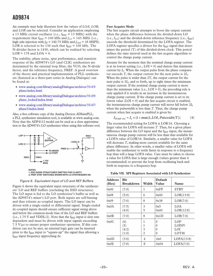
Figure 6. Equivalent Input of LO and REF Buffers
Figure 6 shows the equivalent input structures of the synthesiz-ers’ LO and REF buffers (excluding the ESD structures).The LO input is fed to the LO synthesizer’s buffer as well asthe AD9874’s mixer’s LO port. Both inputs are self-biasingand thus tolerate ac-coupled inputs. The LO input can bedriven with a single-ended or differential signal. Single-endeddc-coupled inputs should ensure sufficient signal swing aboveand below the common-mode bias of the LO and REF buffers(i.e., 1.75 V and VDDL/2). Note that the fREF input is slew ratedependent and must be driven with input signals exceeding7.5 V/s to ensure proper synthesizer operation. If this con-dition can not be met, an external logic gate can be insertedprior to the fREF input to “square-up” the signal thus allowing afREF input frequency approching dc.
Fast Acquire ModeThe fast acquire circuit attempts to boost the output currentwhen the phase difference between the divided-down LO(i.e., fLO) and the divided-down reference frequency (i.e., fREF)exceeds the threshold determined by the LOFA register. TheLOFA register specifies a divisor for the fREF signal that deter-mines the period (T) of this divided-down clock. This perioddefines the time interval used in the fast acquire algorithm tocontrol the charge pump current.
Assume for the moment that the nominal charge pump currentis at its lowest setting (i.e., LOI = 0) and denote this minimumcurrent by I0. When the output pulse from the phase compara-tor exceeds T, the output current for the next pulse is 2I0.When the pulse is wider than 2T, the output current for thenext pulse is 3I0, and so forth, up to eight times the minimumoutput current. If the nominal charge pump current is morethan the minimum value (i.e., LOI > 0), the preceding rule isonly applied if it results in an increase in the instantaneouscharge pump current. If the charge pump current is set to itslowest value (LOI = 0) and the fast acquire circuit is enabled,the instantaneous charge pump current will never fall below 2I0
when the pulsewidth is less than T. Thus, the charge pumpcurrent when fast acquire is enabled is given by:
I I LOI Pulsewidth TPUMP FA− = × +0 1 1 max( , , ) (4)
The recommended setting for LOFA is LOR/16. Choosing alarger value for LOFA will increase T. Thus, for a given phasedifference between the LO input and the fREF input, the instan-taneous charge pump current will be less than that available fora LOFA value of LOR/16. Similarly, a smaller value for LOFAwill decrease T, making more current available for the samephase difference. In other words, a smaller value of LOFA willenable the synthesizer to settle faster in response to a frequencyhop than will a large LOFA value. Care must be taken to choosea value for LOFA that is large enough (values greater than 4recommended) to prevent the loop from oscillating back andforth in response to a frequency hop.
Table VII. SPI Registers Associated with LO Synthesizer
Address Bit Default(Hex) Breakdown Width Value Name
0x00 (7:0) 1 0xFF STBY
0x08 (5:0) 6 0x00 LOR(13:8)
0x09 (7:0) 8 0x38 LOR(7:0)
0x0A (7:5) 3 0x5 LOA(4:0) 5 0x00 LOB(12:8)
0x0B (7:0) 8 0x1D LOB(7:0)
0x0C (6) 1 0 LOF(5) 1 0 LOINV(4:2) 3 0 LOI(1:0) 2 0 LOTM
0x0D (3:0) 4 0x0 LOFA(13:8)
0x0E (7:0) 8 0x04 LOFA(7:0)
REV. A
AD9874
–21–
CLOCK SYNTHESIZERThe clock synthesizer is a fully programmable integer-N PLLcapable of 2.2 kHz resolution at clock input frequencies up to18 MHz and reference frequencies up to 25 MHz. It is similarto the LO synthesizer described in Figure 5 with the followingexceptions:
• It does not include an 8/9 prescaler nor an A counter.
• It includes a negative-resistance core that, when used in conjunc-tion with an external LC tank and varactor, serves as the VCO.
The 14-bit reference counter and 13-bit N-divider counter canbe programmed via registers CKR and CKN. The clockfrequency, fCLK, is related to the reference frequency by theequation
f CKN CKR fCLK REF= ( ) × (5)
The charge pump current is programmable via the CKI registerfrom 0.625 mA to 5.0 mA using the equation:
I CKI mAPUMP = +( ) ×1 0 625. (6)
The fast acquire subcircuit of the charge pump is controlled bythe CKFA register in the same manner as the LO synthesizer iscontrolled by the LOFA register. An on-chip lock detect func-tion (enabled by the CKF bit) automatically increases theoutput current for faster settling during channel changes. Thesynthesizer may also be disabled using the CK standby bitlocated in the STBY register.
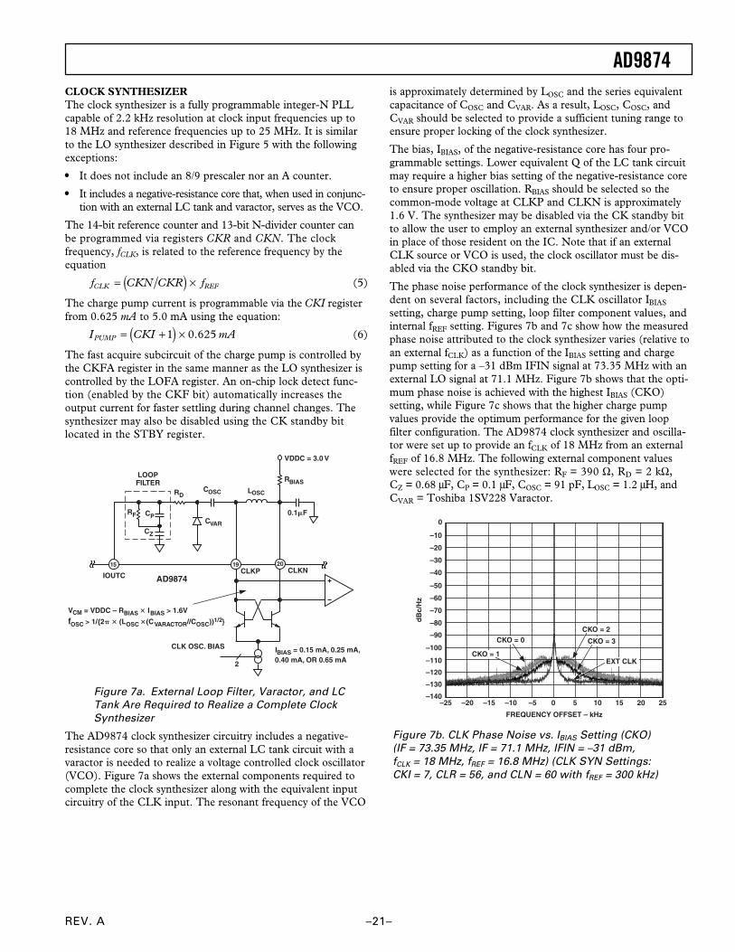
2
CLK OSC. BIAS IBIAS = 0.15 mA, 0.25 mA,0.40 mA, OR 0.65 mA
VDDC = 3.0 V
IOUTC
LOSC
0.1F
RBIASCOSC
LOOPFILTER
CVAR
RD
AD9874CLKNCLKP
VCM = VDDC – RBIAS IBIAS > 1.6V
fOSC > 1/2 (LOSC (CVARACTOR//COSC))1/2
CP
CZ
RF
Figure 7a. External Loop Filter, Varactor, and LCTank Are Required to Realize a Complete ClockSynthesizer
The AD9874 clock synthesizer circuitry includes a negative-resistance core so that only an external LC tank circuit with avaractor is needed to realize a voltage controlled clock oscillator(VCO). Figure 7a shows the external components required tocomplete the clock synthesizer along with the equivalent inputcircuitry of the CLK input. The resonant frequency of the VCO
is approximately determined by LOSC and the series equivalentcapacitance of COSC and CVAR. As a result, LOSC, COSC, andCVAR should be selected to provide a sufficient tuning range toensure proper locking of the clock synthesizer.
The bias, IBIAS, of the negative-resistance core has four pro-grammable settings. Lower equivalent Q of the LC tank circuitmay require a higher bias setting of the negative-resistance coreto ensure proper oscillation. RBIAS should be selected so thecommon-mode voltage at CLKP and CLKN is approximately1.6 V. The synthesizer may be disabled via the CK standby bitto allow the user to employ an external synthesizer and/or VCOin place of those resident on the IC. Note that if an externalCLK source or VCO is used, the clock oscillator must be dis-abled via the CKO standby bit.
The phase noise performance of the clock synthesizer is depen-dent on several factors, including the CLK oscillator IBIAS
setting, charge pump setting, loop filter component values, andinternal fREF setting. Figures 7b and 7c show how the measuredphase noise attributed to the clock synthesizer varies (relative toan external fCLK) as a function of the IBIAS setting and chargepump setting for a –31 dBm IFIN signal at 73.35 MHz with anexternal LO signal at 71.1 MHz. Figure 7b shows that the opti-mum phase noise is achieved with the highest IBIAS (CKO)setting, while Figure 7c shows that the higher charge pumpvalues provide the optimum performance for the given loopfilter configuration. The AD9874 clock synthesizer and oscilla-tor were set up to provide an fCLK of 18 MHz from an externalfREF of 16.8 MHz. The following external component valueswere selected for the synthesizer: RF = 390 Ω, RD = 2 kΩ,CZ = 0.68 µF, CP = 0.1 µF, COSC = 91 pF, LOSC = 1.2 µH, andCVAR = Toshiba 1SV228 Varactor.
–25
0
–90
–100
–110
–120
dB
c/H
z
–20 –15 –10 –5 0 5 10 15 20 25
FREQUENCY OFFSET – kHz
–80
–70
–60
–50
–40
–30
–20
–10
–130
–140
CKO = 1
CKO = 0CKO = 2
CKO = 3
EXT CLK
Figure 7b. CLK Phase Noise vs. IBIAS Setting (CKO) (IF = 73.35 MHz, IF = 71.1 MHz, IFIN = –31 dBm, fCLK = 18 MHz, fREF = 16.8 MHz) (CLK SYN Settings: CKI = 7, CLR = 56, and CLN = 60 with fREF = 300 kHz)
REV. A
AD9874
–22–
–25
0
–90
–100
–110
–120
dB
c/H
z
–20 –15 –10 –5 0 5 10 15 20 25FREQUENCY OFFSET – kHz
–80
–70
–60
–50
–40
–30
–20
–10
–130
–140
CP = 0
CP = 2 CP = 4CP = 6
EXT CLK
Figure 7c. CLK Phase Noise vs. Charge Pump Setting Bias(IF = 73.35 MHz, IF = 71.1 MHz, –31 dBm, fCLK = 18 MHz,fREF = 16.8 MHz) (CLK SYN Settings: CKO Bias = 3, CKR = 56,and CKN = 60 with fREF = 300 kHz)
Table VIII. SPI Registers Associated with CLK Synthesizer
Address Bit Default(Hex) Breakdown Width Value Name
0x00 (7:0) 8 0xFF STBY
0x01 (3:2) 2 0 CKOB
0x10 (5:0) 6 00 CKR(13:8)
0x11 (7:0) 8 0x38 CKR(7:0)
0x12 (4:0) 5 0x00 CKN(12:8)
0x13 (7:0) 8 0x3C CKN(7:0)
0x14 (6) 1 0 CKF(5) 1 0 CKINV(4:2) 3 0 CKI(1:0) 1 0 CKTM
0x15 (3:0) 4 0x0 CKFA(13:8)
0x16 (7:0) 8 0x04 CKFA(7:0)
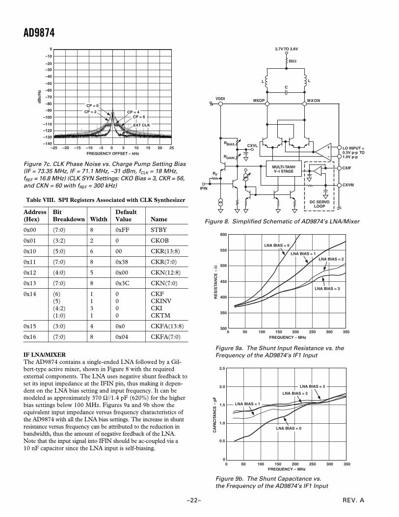
IF LNA/MIXERThe AD9874 contains a single-ended LNA followed by a Gil-bert-type active mixer, shown in Figure 8 with the requiredexternal components. The LNA uses negative shunt feedback toset its input impedance at the IFIN pin, thus making it depen-dent on the LNA bias setting and input frequency. It can bemodeled as approximately 370 Ω//1.4 pF (620%) for the higherbias settings below 100 MHz. Figures 9a and 9b show theequivalent input impedance versus frequency characteristics ofthe AD9874 with all the LNA bias settings. The increase in shuntresistance versus frequency can be attributed to the reduction inbandwidth, thus the amount of negative feedback of the LNA.Note that the input signal into IFIN should be ac-coupled via a10 nF capacitor since the LNA input is self-biasing.
RF
IFIN
RGAIN
RBIAS
VDDI MXOP
LO INPUT =0.3V p-p TO1.0V p-p
DC SERVOLOOP
MULTI-TANHV–I STAGE
CXIF
MXON
CXVM
50
CL L
CXVL
2.7V TO 3.6V
Figure 8. Simplified Schematic of AD9874’s LNA/Mixer
FREQUENCY – MHz
500
100
400
600
200
RE
SIS
TAN
CE
–
0
550
450
15050
350
300350300250
LNA BIAS = 0
LNA BIAS = 1LNA BIAS = 2
LNA BIAS = 3
Figure 9a. The Shunt Input Resistance vs. theFrequency of the AD9874’s IF1 Input
FREQUENCY – MHz
1.5
100
0.5
2.5
200
CA
PAC
ITA
NC
E –
pF
0
2.0
1.0
150500
350300250
LNA BIAS = 3
LNA BIAS = 2
LNA BIAS = 1
LNA BIAS = 0
Figure 9b. The Shunt Capacitance vs.the Frequency of the AD9874’s IF1 Input
REV. A
AD9874
–23–
The mixer’s differential LO port is driven by the LO bufferstage shown in Figure 6, which can be driven single-ended ordifferential. Since it is self-biasing, the LO signal level can beac-coupled and range from 0.3 V p-p to 1.0 V p-p with negligibleeffect on performance. The mixer’s open-collector outputs,MXOP and MXON, drive an external resonant tank consistingof a differential LC network tuned to the IF of the band-pass- ADC (i.e., fIF2_ADC = fCLK/8). The two inductors provide adc bias path for the mixer core via a series resistor of 50 Ω, whichis included to dampen the common-mode response. The mixer’soutput must be ac-coupled to the input of the band-pass - ADC,IF2P, and IF2N via two 100 pF capacitors to ensure proper tuningof the LC center frequency.
The external differential LC tank forms the resonant elementfor the first resonator of the band-pass - modulator, and somust be tuned to the fCLK/8 center frequency of the modulator.The inductors should be chosen such that their impedance atfCLK/8 is about 140 Ω (i.e., L = 180/fCLK). An accuracy of 20%is considered to be adequate. For example, at fCLK = 18 MHz,L = 10 µH is a good choice. Once the inductors have beenselected, the required tank capacitance may be calculated usingthe relation fCLK/8 = 1/2 (2L C)1/2.
For example, at fCLK = 18 MHz and L = 10 µH, a capacitance of250 pF is needed. However, in order to accommodate an induc-tor tolerance of 10%, the tank capacitance must be adjustablefrom 227 pF to 278 pF. Selecting an external capacitor of180 pF ensures that even with a 10% tolerance and stray capaci-tances as high as 30 pF, the total capacitance will be less thanthe minimum value needed by the tank. Extra capacitance issupplied by the AD9874’s on-chip programmable capacitorarray. Since the programming range of the capacitor array is atleast 160 pF, the AD9874 has plenty of range to make up forthe tolerances of low cost external components. Note that if fCLK
is increased by a factor of 1.44 MHz to 26 MHz so that fCLK/8becomes 3.25 MHz, reducing L and C by approximately thesame factor (i.e., L = 6.9 µH and C = 120 pF) still satisfies therequirements stated above.
The selection of the inductors is an important consideration inrealizing the full linearity performance of the AD9874. This istrue when operating the LNA and mixer at maximum bias andlow clock frequency. Figure 10 shows how the two-tone input-referred IMD versus the input level performance at an IF of109 MHz and fCLK of 18 MHz varies between Toko’s FSLMseries and Coilcraft’s 1812CS series inductors. The graph alsoshows the extrapolated point of intersection used to determinethe IIP3 performance. Note that the Coilcraft inductor providesa 7 dB to 8 dB improvement in performance and closelyapproximates the 3:1 slope associated with a third orderlinearity compared to the 2.65:1 slope associated with theToko inductor. The Coilcraft 1008CS series showed perfor-mance similar to that of the 1812CS series. It is worth notingthat the difference in IMD performance between these twoinductor families with an fCLK of 26 MHz is insignificant.
–30 –24 –18–36–48 –42–54
0
–20
–40
–60
–80
–100
–120
–140
INP
UT
RE
FE
RR
ED
PO
WE
R –
dB
m
TOKO INDUCTORPIMD = 2.64 PIN + 4.6
PIN
fIN = 109.65MHz
COILCRAFTPIMD = 2.92 PIN + 6.9
Figure 10. IMD Performance between Different Inductorswith LNA and Mixer at Full Bias and fCLK of 18 MHz
Both the LNA and mixer have four programmable bias settings sothat current consumption can be minimized for a given application.Figures 11a, 11b, and 11c show how the LNA and mixer’s noisefigure (NF), linearity (IIP3), IF clip point, current consumption,and frequency response are affected for a given LNA/mixer biassetting. The measurements were taken at an IF = 73.35 MHz andLO = 71.1 MHz, with supplies set to 3 V.
1_0
13
12
11
10
9
8
NO
ISE
FIG
UR
E –
dB
1_1 1_2 1_3 2_0 2_1 2_2 2_3 3_0 3_1 3_2 3_3
–20
–18
–16
–14
–12
–10
CL
IP P
OIN
T –
dB
m
CLIP POINT
NOISE FIGURE
LNA_MIXER BIAS SETTING
Figure 11a. LNA/Mixer Noise Figure andConversion Gain vs. Bias Setting
1_0
5
0
–5
–10
–15
–25
INP
UT
IIP
3 –
dB
m
1_1 1_2 1_3 2_0 2_1 2_2 2_3 3_0 3_1 3_2 3_3
7.00
8.25
5.75
4.50
3.25
2.00
IDD
I – m
A9.50
–20
LNA_MIXER CURRENT
IIP3
LNA_MIXER BIAS SETTING
Figure 11b. LNA/Mixer IIP3 and CurrentConsumption vs. Bias Setting
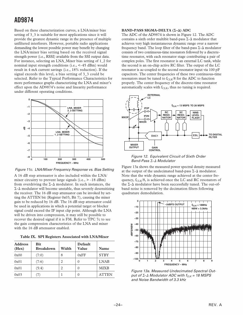
REV. A
AD9874
–24–
Based on these characterization curves, a LNA/mixer biassetting of 3_3 is suitable for most applications since it willprovide the greatest dynamic range in the presence of multipleunfiltered interferers. However, portable radio applicationsdemanding the lowest possible power may benefit by changingthe LNA/mixer bias setting based on the received signalstrength power (i.e., RSSI) available from the SSI output data.For instance, selecting an LNA_Mixer bias setting of 1_2 fornominal input strength conditions (i.e., <–45 dBm) wouldresult in 4 mA current savings (i.e., 18% reduction). If thesignal exceeds this level, a bias setting of 3_3 could beselected. Refer to the Typical Performance Characteristics formore performance graphs characterizing the LNA and mixer’seffect upon the AD9874’s noise and linearity performanceunder different operating conditions.
0
0
–1
–2
–3
–5
dB
100 200 300 400 500
–4
FREQUENCY – MHz
–6
–7
–8
LNA_MIXER1_2 SETTING
LNA_MIXER3_3 SETTING
Figure 11c. LNA/Mixer Frequency Response vs. Bias Setting
A 16 dB step attenuator is also included within the LNA/mixer circuitry to prevent large signals (i.e., > –18 dBm)from overdriving the - modulator. In such instances, the- modulator will become unstable, thus severely desensitizingthe receiver. The 16 dB step attenuator can be invoked by set-ting the ATTEN bit (Register 0x03, Bit 7), causing the mixergain to be reduced by 16 dB. The 16 dB step attenuator couldbe used in applications in which a potential target or blockersignal could exceed the IF input clip point. Although the LNAwill be driven into compression, it may still be possible torecover the desired signal if it is FM. Refer to TPC 7c to seethe gain compression characteristics of the LNA and mixerwith the 16 dB attenuator enabled.
Table IX. SPI Registers Associated with LNA/Mixer
Address Bit Default(Hex) Breakdown Width Value Name
0x00 (7:0) 8 0xFF STBY
0x01 (7:6) 2 0 LNAB
0x01 (5:4) 2 0 MIXB
0x03 (7) 1 0 ATTEN
BAND-PASS SIGMA-DELTA (-) ADCThe ADC of the AD9874 is shown in Figure 12. The ADCcontains a sixth order multibit band-pass - modulator thatachieves very high instantaneous dynamic range over a narrowfrequency band. The loop filter of the band-pass - modulatorconsists of two continuous-time resonators followed by a discrete-time resonator, with each resonator stage contributing a pair ofcomplex poles. The first resonator is an external LC tank, whilethe second is an on-chip active RC filter. The output of the LCresonator is ac-coupled to the second resonator input via 100 pFcapacitors. The center frequencies of these two continuous-timeresonators must be tuned to fCLK/8 for the ADC to functionproperly. The center frequency of the discrete-time resonatorautomatically scales with fCLK, thus no tuning is required.
TO DIGITALFILTER
SCRESO-NATOR
NINE-LEVELFLASH
ESL
GAINCONTROL
MIXEROUTPUT
EXTERNALLC
fCLK = 13 MSPS TO 26 MSPS
MXOP
MXON
IF2P
IF2N
RCRESO-NATOR
DAC1
Figure 12. Equivalent Circuit of Sixth OrderBand-Pass - Modulator
Figure 13a shows the measured power spectral density measuredat the output of the undecimated band-pass - modulator.Note that the wide dynamic range achieved at the center fre-quency, fCLK/8, is achieved once the LC and RC resonators ofthe - modulator have been successfully tuned. The out-of-band noise is removed by the decimation filters followingquadrature demodulation.
0
0
–10
–20
–30
–50
dB
FS
/NB
W –40
FREQUENCY – MHz
–60
–70
–80
–90
–1001 2 3 4 5 6 7 8 9
–2dBFS OUTPUT fCLK = 18MHz
NBW = 3.3kHz
Figure 13a. Measured Undecimated Spectral Out-put of - Modulator ADC with fCLK = 18 MSPSand Noise Bandwidth of 3.3 kHz
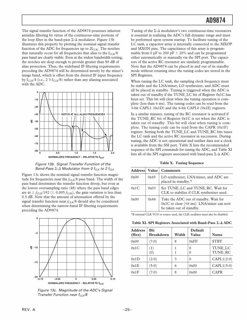
REV. A
AD9874
–25–
The signal transfer function of the AD9874 possesses inherentantialias filtering by virtue of the continuous-time portions ofthe loop filter in the band-pass - modulator. Figure 13billustrates this property by plotting the nominal signal transferfunction of the ADC for frequencies up to 2fCLK. The notchesthat naturally occur for all frequencies that alias to the fCLK/8pass band are clearly visible. Even at the widest bandwidth setting,the notches are deep enough to provide greater than 80 dB ofalias protection. Thus, the wideband IF filtering requirementspreceding the AD9874 will be determined mostly by the mixer’simage band, which is offset from the desired IF input frequencyby fCLK/4 (i.e., 2 3 fCLK/8) rather than any aliasing associatedwith the ADC.
0
0
–10
–20
–30
–50
dB –40
NORMALIZED FREQUENCY – RELATIVE TO fOUT
–60
–70
–800.5 1.0 1.5 2.0
NOTCH AT ALL ALIAS FREQUENCIES
Figure 13b. Signal Transfer Function of theBand-Pass - Modulator from 0 fCLK to 2 fCLK
Figure 13c shows the nominal signal transfer function magni-tude for frequencies near the fCLK/8 pass band. The width of thepass band determines the transfer function droop, but even atthe lowest oversampling ratio (48) where the pass band edgesare at fCLK/192 ( 0.005 fCLK), the gain variation is less than0.5 dB. Note that the amount of attenuation offered by thesignal transfer function near fCLK/8 should also be consideredwhen determining the narrow-band IF filtering requirementspreceding the AD9874.
–0.10
0
–5
dB –10
NORMALIZED FREQUENCY – RELATIVE TO fCLK
–15
–20–0.05 0 0.05 0.10
Figure 13c. Magnitude of the ADC’s SignalTransfer Function near fCLK/8
Tuning of the - modulator’s two continuous-time resonatorsis essential in realizing the ADC’s full dynamic range and mustbe performed upon system startup. To facilitate tuning of theLC tank, a capacitor array is internally connected to the MXOPand MXON pins. The capacitance of this array is program-mable from 0 pF to 200 pF 20% and can be programmedeither automatically or manually via the SPI port. The capaci-tors of the active RC resonator are similarly programmable.Note that the AD9874 can be placed in and out of its standbymode without retuning since the tuning codes are stored in theSPI Registers.
When tuning the LC tank, the sampling clock frequency mustbe stable and the LNA/mixer, LO synthesizer, and ADC mustall be placed in standby. Tuning is triggered when the ADC istaken out of standby if the TUNE_LC bit of Register 0x1C hasbeen set. This bit will clear when the tuning operation is com-plete (less than 6 ms). The tuning codes can be read from the3-bit CAPL1 (0x1D) and the 6-bit CAPL0 (0x1E) registers.
In a similar manner, tuning of the RC resonator is activated ifthe TUNE_RC bit of Register 0x1C is set when the ADC istaken out of standby. This bit will clear when tuning is com-plete. The tuning code can be read from the CAPR (0x1F)register. Setting both the TUNE_LC and TUNE_RC bits tunesthe LC tank and the active RC resonator in succession. Duringtuning, the ADC is not operational and neither data nor a clockis available from the SSI port. Table X lists the recommendedsequence of the SPI commands for tuning the ADC, and Table XIlists all of the SPI registers associated with band-pass - ADC.
Table X. Tuning Sequence
Address Value Comments
0x00 0x45 LO synthesizer, LNA/mixer, and ADC areplaced in standby.*
0x1C 0x03 Set TUNE_LC and TUNE_RC. Wait forCLK to stabilize if CLK synthesizer used.
0x00 0x44 Take the ADC out of standby. Wait for0x1C to clear (<6 ms). LNA/mixer can nowbe taken out of standby.
*If external CLK VCO or source used, the CLK oscillator must also be disabled.
Table XI. SPI Registers Associated with Band-Pass - ADC
Address Bit Default(Hex) Breakdown Width Value Name
0x00 (7:0) 8 0xFF STBY
0x1C (1) 1 0 TUNE_LC(0) 1 0 TUNE_RC
0x1D (2:0) 3 0 CAPL1(2:0)
0x1E (5:0) 6 0x00 CAPL1(5:0)
0x1F (7:0) 8 0x00 CAPR
REV. A
AD9874
–26–
Once the AD9874 has been tuned, the noise figure degradationattributed solely to the temperature drift of the LC and RCresonators is minimal. Since the drift of the RC resonator isactually negligible compared to that of the LC resonator, theexternal L and C components’ temperature drift characteristicstend to dominate. Figure 13d shows the degradation in noisefigure as the product of the LC value is allowed to vary from–12.5% to +12.5%. Note that the noise figure remains relativelyconstant over a 3.5% range (i.e., 35,000 ppm), suggestingthat most applications will not be required to retune over theoperating temperature range.
–15
12
11
NF
– d
B
10
LC ERROR – %
9
80 5 10 15–5–10
BW = 75kHz
BW = 10kHz
BW = 30kHz
Figure 13d. Typical Noise Figure Degradationfrom L and C Component Drift (fCLK = 18 MSPS,fIF = 73.3501 MHz)
DECIMATION FILTERThe decimation filter shown in Figure 14 consists of an fCLK/8complex mixer and a cascade of three linear phase FIR filters:DEC1, DEC2, and DEC3. DEC1 downsamples by a factor of12 using a fourth order comb filter. DEC2 also uses a fourthorder comb filter, but its decimation factor is set by the M fieldof Register 0x07. DEC3 is either a decimate-by-5 FIR filter or adecimate-by-4 FIR filter, depending on the value of the K bitwithin Register 0x07. Thus, the composite decimation factorcan be set to either 60 M or 48 M for K equal to 0 or 1,respectively.
The output data rate (fOUT) is equal to the modulator clockfrequency (fCLK) divided by the digital filter’s decimation factor.Due to the transition region associated with the decimationfilter’s frequency response, the decimation factor must beselected such that fOUT is equal to or greater than twice thesignal bandwidth. This ensures low amplitude ripple in the passband along with the ability to provide further application-spe-cific digital filtering prior to demodulation.
4 OR 5
COS
SINDATAFROM -
MODULATOR
DEC1
SINC4
FILTER12
DEC2
SINC4
FILTERM + 1
M
DEC3
FIRFILTER
K
I
Q
COMPLEXDATA TOSSI PORT
Figure 14. Decimation Filter Architecture
Figure 15a shows the response of the decimation filter at adecimation factor of 900 (K = 0, M = 14) and a samplingclock frequency of 18 MHz. In this example, the output datarate (fOUT) is 20 kSPS, with a usable complex signal band-width of 10 kHz centered around dc. As this figure shows,the first and second alias bands (occurring at even integermultiples of fOUT/2) have the least attenuation but provide atleast 88 dB of attenuation. Note that signals falling aroundfrequency offsets that are odd integer multiples of fOUT/2(i.e., 10 kHz, 30 kHz, and 50 kHz) will fall back into thetransition band of the digital filter.
FREQUENCY – kHz
0
–40
–100
0 3010 20
–20
–60
–80
40 100
dB
FOLD-ING
POINT
5.0kHz PASS BAND
–12070 806050 90
–88dB –88dB
–101dB –103dB
Figure 15a. Decimation Filter Frequency Responsefor fOUT = 20 kSPS (fCLK = 18 MHz, OSR = 900)
Figure 15b shows the response of the decimation filter with adecimation factor of 48 and a sampling clock rate of 26 MHz. Thealias attenuation is at least 94 dB and occurs for frequencies at theedges of the fourth alias band. The difference between the aliasattenuation characteristics of Figure 15b and those of Figure 15a isdue to the fact that the third decimation stage decimates by a factorof 5 for Figure 15a compared with a factor of 4 for Figure 15b.
0
–40
–100
–20
–60
–80
dB
–120
FREQUENCY – MHz
0 1.50.5 1.0 2.0 2.5
135.466kHz PASS BAND
–98dB
–115dB–94dB
Figure 15b. Decimation Filter Frequency Responsefor fOUT = 541.666 kSPS (fCLK = 26 MHz, OSR = 48)
REV. A
AD9874
–27–
Figures 16a and 16b show expanded views of the pass band for thetwo possible configurations of the third decimation filter. Whendecimating by 60n (K = 0), the pass-band gain variation is 1.2 dB;when decimating by 48n (K = 1), the pass-band gain variation is0.9 dB. Normalization of full scale at band center is accurate towithin 0.14 dB across all decimation modes. Figures 17a and 17bshow the folded frequency response of the decimator for K = 0and K = 1, respectively.
NORMALIZED FREQUENCY – RELATIVE TO fOUT
0
3
0.250
dB
0.125
2
1
0
–1
–2
–3
PASS-BAND GAIN FREQUENCY = 1.2dB
Figure 16a. Pass-Band Frequency Response ofthe Decimator for K = 0
NORMALIZED FREQUENCY – RELATIVE TO fOUT
0
3
0.250
dB
0.125
2
1
0
–1
–2
–3
PASS-BAND GAIN VARIATION = 0.9dB
Figure 16b. Pass-Band Frequency Response ofthe Decimator for K = 1
NORMALIZED FREQUENCY – RELATIVE TO fOUT
0
0
0.50
dB
0.25
–20
–40
–60
–80
–100
–120
MIN ALIAS ATTN = 87.7dB
Figure 17a. Folded Decimator Frequency Response for K = 0
NORMALIZED FREQUENCY – RELATIVE TO fOUT
0
0
0.50
dB
0.25
–20
–40
–60
–80
–100
–120
MIN ALIAS ATTN = 97.2dB
Figure 17b. Folded Decimator Frequency Response for K = 1
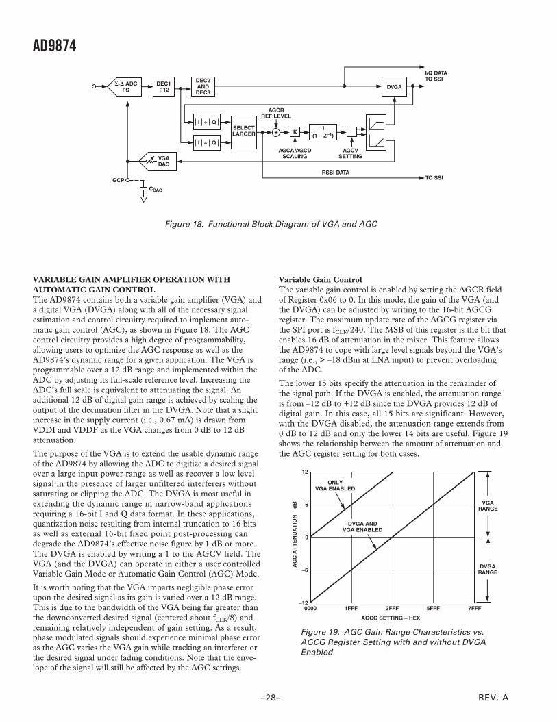
REV. A
AD9874
–28–
VARIABLE GAIN AMPLIFIER OPERATION WITHAUTOMATIC GAIN CONTROLThe AD9874 contains both a variable gain amplifier (VGA) anda digital VGA (DVGA) along with all of the necessary signalestimation and control circuitry required to implement auto-matic gain control (AGC), as shown in Figure 18. The AGCcontrol circuitry provides a high degree of programmability,allowing users to optimize the AGC response as well as theAD9874’s dynamic range for a given application. The VGA isprogrammable over a 12 dB range and implemented within theADC by adjusting its full-scale reference level. Increasing theADC’s full scale is equivalent to attenuating the signal. Anadditional 12 dB of digital gain range is achieved by scaling theoutput of the decimation filter in the DVGA. Note that a slightincrease in the supply current (i.e., 0.67 mA) is drawn fromVDDI and VDDF as the VGA changes from 0 dB to 12 dBattenuation.
The purpose of the VGA is to extend the usable dynamic rangeof the AD9874 by allowing the ADC to digitize a desired signalover a large input power range as well as recover a low levelsignal in the presence of larger unfiltered interferers withoutsaturating or clipping the ADC. The DVGA is most useful inextending the dynamic range in narrow-band applicationsrequiring a 16-bit I and Q data format. In these applications,quantization noise resulting from internal truncation to 16 bitsas well as external 16-bit fixed point post-processing candegrade the AD9874’s effective noise figure by 1 dB or more.The DVGA is enabled by writing a 1 to the AGCV field. TheVGA (and the DVGA) can operate in either a user controlledVariable Gain Mode or Automatic Gain Control (AGC) Mode.
It is worth noting that the VGA imparts negligible phase errorupon the desired signal as its gain is varied over a 12 dB range.This is due to the bandwidth of the VGA being far greater thanthe downconverted desired signal (centered about fCLK/8) andremaining relatively independent of gain setting. As a result,phase modulated signals should experience minimal phase erroras the AGC varies the VGA gain while tracking an interferer orthe desired signal under fading conditions. Note that the enve-lope of the signal will still be affected by the AGC settings.
Variable Gain ControlThe variable gain control is enabled by setting the AGCR fieldof Register 0x06 to 0. In this mode, the gain of the VGA (andthe DVGA) can be adjusted by writing to the 16-bit AGCGregister. The maximum update rate of the AGCG register viathe SPI port is fCLK/240. The MSB of this register is the bit thatenables 16 dB of attenuation in the mixer. This feature allowsthe AD9874 to cope with large level signals beyond the VGA’srange (i.e., > –18 dBm at LNA input) to prevent overloadingof the ADC.
The lower 15 bits specify the attenuation in the remainder ofthe signal path. If the DVGA is enabled, the attenuation rangeis from –12 dB to +12 dB since the DVGA provides 12 dB ofdigital gain. In this case, all 15 bits are significant. However,with the DVGA disabled, the attenuation range extends from0 dB to 12 dB and only the lower 14 bits are useful. Figure 19shows the relationship between the amount of attenuation andthe AGC register setting for both cases.
AGCG SETTING – HEX
–12
0
12
0000
AG
C A
TT
EN
UA
TIO
N –
dB
1FFF 3FFF 7FFF5FFF
6
–6
VGARANGE
DVGARANGE
ONLYVGA ENABLED
DVGA ANDVGA ENABLED
Figure 19. AGC Gain Range Characteristics vs.AGCG Register Setting with and without DVGAEnabled
+
VGADAC
- ADCFS
DEC112
DEC2ANDDEC3
I + Q
I + Q
SELECTLARGER
AGCRREF LEVEL
K
AGCA/AGCDSCALING
CDAC
GCP
1(1 – Z–1)
AGCVSETTING
DVGA
RSSI DATATO SSI
I/Q DATATO SSI
Figure 18. Functional Block Diagram of VGA and AGC
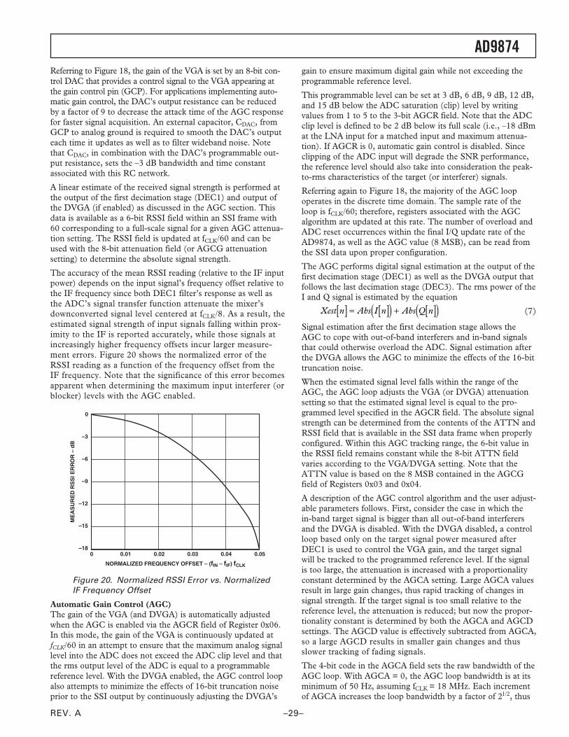
REV. A
AD9874
–29–
Referring to Figure 18, the gain of the VGA is set by an 8-bit con-trol DAC that provides a control signal to the VGA appearing atthe gain control pin (GCP). For applications implementing auto-matic gain control, the DAC’s output resistance can be reducedby a factor of 9 to decrease the attack time of the AGC responsefor faster signal acquisition. An external capacitor, CDAC, fromGCP to analog ground is required to smooth the DAC’s outputeach time it updates as well as to filter wideband noise. Notethat CDAC, in combination with the DAC’s programmable out-put resistance, sets the –3 dB bandwidth and time constantassociated with this RC network.
A linear estimate of the received signal strength is performed atthe output of the first decimation stage (DEC1) and output ofthe DVGA (if enabled) as discussed in the AGC section. Thisdata is available as a 6-bit RSSI field within an SSI frame with60 corresponding to a full-scale signal for a given AGC attenua-tion setting. The RSSI field is updated at fCLK/60 and can beused with the 8-bit attenuation field (or AGCG attenuationsetting) to determine the absolute signal strength.
The accuracy of the mean RSSI reading (relative to the IF inputpower) depends on the input signal’s frequency offset relative tothe IF frequency since both DEC1 filter’s response as well asthe ADC’s signal transfer function attenuate the mixer’sdownconverted signal level centered at fCLK/8. As a result, theestimated signal strength of input signals falling within prox-imity to the IF is reported accurately, while those signals atincreasingly higher frequency offsets incur larger measure-ment errors. Figure 20 shows the normalized error of theRSSI reading as a function of the frequency offset from theIF frequency. Note that the significance of this error becomesapparent when determining the maximum input interferer (orblocker) levels with the AGC enabled.
0
0
–3
ME
AS
UR
ED
RS
SI E
RR
OR
– d
B
–6
NORMALIZED FREQUENCY OFFSET – (fIN – fIF) fCLK
–9
–180.03 0.04 0.050.020.01
–12
–15
Figure 20. Normalized RSSI Error vs. NormalizedIF Frequency Offset
Automatic Gain Control (AGC)The gain of the VGA (and DVGA) is automatically adjustedwhen the AGC is enabled via the AGCR field of Register 0x06.In this mode, the gain of the VGA is continuously updated atfCLK/60 in an attempt to ensure that the maximum analog signallevel into the ADC does not exceed the ADC clip level and thatthe rms output level of the ADC is equal to a programmablereference level. With the DVGA enabled, the AGC control loopalso attempts to minimize the effects of 16-bit truncation noiseprior to the SSI output by continuously adjusting the DVGA’s
gain to ensure maximum digital gain while not exceeding theprogrammable reference level.
This programmable level can be set at 3 dB, 6 dB, 9 dB, 12 dB,and 15 dB below the ADC saturation (clip) level by writingvalues from 1 to 5 to the 3-bit AGCR field. Note that the ADCclip level is defined to be 2 dB below its full scale (i.e., –18 dBmat the LNA input for a matched input and maximum attenua-tion). If AGCR is 0, automatic gain control is disabled. Sinceclipping of the ADC input will degrade the SNR performance,the reference level should also take into consideration the peak-to-rms characteristics of the target (or interferer) signals.
Referring again to Figure 18, the majority of the AGC loopoperates in the discrete time domain. The sample rate of theloop is fCLK/60; therefore, registers associated with the AGCalgorithm are updated at this rate. The number of overload andADC reset occurrences within the final I/Q update rate of theAD9874, as well as the AGC value (8 MSB), can be read fromthe SSI data upon proper configuration.
The AGC performs digital signal estimation at the output of thefirst decimation stage (DEC1) as well as the DVGA output thatfollows the last decimation stage (DEC3). The rms power of theI and Q signal is estimated by the equation
Xest n Abs I n Abs Q n[ ] = [ ]( ) + [ ]( ) (7)
Signal estimation after the first decimation stage allows theAGC to cope with out-of-band interferers and in-band signalsthat could otherwise overload the ADC. Signal estimation afterthe DVGA allows the AGC to minimize the effects of the 16-bittruncation noise.
When the estimated signal level falls within the range of theAGC, the AGC loop adjusts the VGA (or DVGA) attenuationsetting so that the estimated signal level is equal to the pro-grammed level specified in the AGCR field. The absolute signalstrength can be determined from the contents of the ATTN andRSSI field that is available in the SSI data frame when properlyconfigured. Within this AGC tracking range, the 6-bit value inthe RSSI field remains constant while the 8-bit ATTN fieldvaries according to the VGA/DVGA setting. Note that theATTN value is based on the 8 MSB contained in the AGCGfield of Registers 0x03 and 0x04.
A description of the AGC control algorithm and the user adjust-able parameters follows. First, consider the case in which thein-band target signal is bigger than all out-of-band interferersand the DVGA is disabled. With the DVGA disabled, a controlloop based only on the target signal power measured afterDEC1 is used to control the VGA gain, and the target signalwill be tracked to the programmed reference level. If the signalis too large, the attenuation is increased with a proportionalityconstant determined by the AGCA setting. Large AGCA valuesresult in large gain changes, thus rapid tracking of changes insignal strength. If the target signal is too small relative to thereference level, the attenuation is reduced; but now the propor-tionality constant is determined by both the AGCA and AGCDsettings. The AGCD value is effectively subtracted from AGCA,so a large AGCD results in smaller gain changes and thusslower tracking of fading signals.
The 4-bit code in the AGCA field sets the raw bandwidth of theAGC loop. With AGCA = 0, the AGC loop bandwidth is at itsminimum of 50 Hz, assuming fCLK = 18 MHz. Each incrementof AGCA increases the loop bandwidth by a factor of 21/2, thus
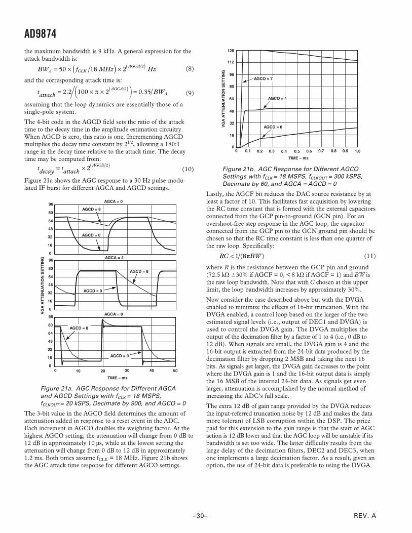
REV. A
AD9874
–30–
the maximum bandwidth is 9 kHz. A general expression for theattack bandwidth is:
BW f MHz HzA CLKAGCA= × ( ) × ( )50 18 2 2 (8)
and the corresponding attack time is:
tattack BWAGCA
A= × ×
=( )2 2 100 2 0 352. .π (9)
assuming that the loop dynamics are essentially those of asingle-pole system.
The 4-bit code in the AGCD field sets the ratio of the attacktime to the decay time in the amplitude estimation circuitry.When AGCD is zero, this ratio is one. Incrementing AGCDmultiplies the decay time constant by 21/2, allowing a 180:1range in the decay time relative to the attack time. The decaytime may be computed from:
tdecay tattack
AGCD= × ( )2 2(10)
Figure 21a shows the AGC response to a 30 Hz pulse-modu-lated IF burst for different AGCA and AGCD settings.
AGCA = 0
80
64
0
48
32
16
96
TIME – ms
10 200 504030
80
64
0
48
32
16
96
VG
A A
TT
EN
UA
TIO
N S
ET
TIN
G AGCA = 4
80
64
0
48
32
16
96
AGCA = 8
AGCD = 8
AGCD = 0
AGCD = 8
AGCD = 0
AGCD = 8
AGCD = 0
Figure 21a. AGC Response for Different AGCAand AGCD Settings with fCLK = 18 MSPS,fCLKOUT = 20 kSPS, Decimate by 900, and AGCO = 0
The 3-bit value in the AGCO field determines the amount ofattenuation added in response to a reset event in the ADC.Each increment in AGCO doubles the weighting factor. At thehighest AGCO setting, the attenuation will change from 0 dB to12 dB in approximately 10 µs, while at the lowest setting theattenuation will change from 0 dB to 12 dB in approximately1.2 ms. Both times assume fCLK = 18 MHz. Figure 21b showsthe AGC attack time response for different AGCO settings.
VG
A A
TT
EN
UA
TIO
N S
ET
TIN
G
TIME – ms
0.1 0.20 0.50.40.3
80
64
0
48
32
16
96
1.00.90.80.70.6
112
128
AGCO = 7
AGCO = 4
AGCD = 0
Figure 21b. AGC Response for Different AGCOSettings with fCLK = 18 MSPS, fCLKOUT = 300 kSPS,Decimate by 60, and AGCA = AGCD = 0
Lastly, the AGCF bit reduces the DAC source resistance by atleast a factor of 10. This facilitates fast acquisition by loweringthe RC time constant that is formed with the external capacitorsconnected from the GCP pin-to-ground (GCN pin). For anovershoot-free step response in the AGC loop, the capacitorconnected from the GCP pin to the GCN ground pin should bechosen so that the RC time constant is less than one quarter ofthe raw loop. Specifically:
RC BW< 1 8( )π (11)
where R is the resistance between the GCP pin and ground(72.5 k 30% if AGCF = 0, < 8 k if AGCF = 1) and BW isthe raw loop bandwidth. Note that with C chosen at this upperlimit, the loop bandwidth increases by approximately 30%.
Now consider the case described above but with the DVGAenabled to minimize the effects of 16-bit truncation. With theDVGA enabled, a control loop based on the larger of the twoestimated signal levels (i.e., output of DEC1 and DVGA) isused to control the DVGA gain. The DVGA multiplies theoutput of the decimation filter by a factor of 1 to 4 (i.e., 0 dB to12 dB). When signals are small, the DVGA gain is 4 and the16-bit output is extracted from the 24-bit data produced by thedecimation filter by dropping 2 MSB and taking the next 16bits. As signals get larger, the DVGA gain decreases to the pointwhere the DVGA gain is 1 and the 16-bit output data is simplythe 16 MSB of the internal 24-bit data. As signals get evenlarger, attenuation is accomplished by the normal method ofincreasing the ADC’s full scale.
The extra 12 dB of gain range provided by the DVGA reducesthe input-referred truncation noise by 12 dB and makes the datamore tolerant of LSB corruption within the DSP. The pricepaid for this extension to the gain range is that the start of AGCaction is 12 dB lower and that the AGC loop will be unstable if itsbandwidth is set too wide. The latter difficulty results from thelarge delay of the decimation filters, DEC2 and DEC3, whenone implements a large decimation factor. As a result, given anoption, the use of 24-bit data is preferable to using the DVGA.
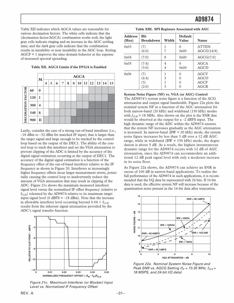
REV. A
AD9874
–31–
Table XII indicates which AGCA values are reasonable forvarious decimation factors. The white cells indicate that the(decimation factor/AGCA) combination works well; the lightgray cells indicate ringing and an increase in the AGC settlingtime; and the dark gray cells indicate that the combinationresults in instability or near instability in the AGC loop. SettingAGCF = 1 improves the time-domain behavior at the expenseof increased spectral spreading.
Table XII. AGCA Limits if the DVGA is Enabled
AGCAM
0
1
4
8
E
60
120
300
540
900
DE
CIM
AT
ION
FA
CT
OR
4 5 6 7 8 9 10 11 12 13 14 15
Lastly, consider the case of a strong out-of-band interferer (i.e.,–18 dBm to –32 dBm for matched IF input) that is larger thanthe target signal and large enough to be tracked by the controlloop based on the output of the DEC1. The ability of the con-trol loop to track this interferer and set the VGA attenuation toprevent clipping of the ADC is limited by the accuracy of thedigital signal estimation occurring at the output of DEC1. Theaccuracy of the digital signal estimation is a function of thefrequency offset of the out-of-band interferer relative to the IFfrequency as shown in Figure 20. Interferers at increasinglyhigher frequency offsets incur larger measurement errors, poten-tially causing the control loop to inadvertently reduce theamount of VGA attenuation that may result in clipping of theADC. Figure 21c shows the maximum measured interferersignal level versus the normalized IF offset frequency (relative tofCLK) tolerated by the AD9874 relative to its maximum targetinput signal level (0 dBFS = –18 dBm). Note that the increasein allowable interferer level occurring beyond 0.04 fCLK
results from the inherent signal attenuation provided by theADC’s signal transfer function.
NORMALIZED FREQUENCY OFFSET = (fIN – fIF)/fCLK
–6
0.02
–12
0
0.040
–3
–9
0.030.01–15
0.05
RE
LAT
IVE
TO
CL
IP P
OIN
T –
dB
FS
Figure 21c. Maximum Interferer (or Blocker) InputLevel vs. Normalized IF Frequency Offset
Table XIII. SPI Registers Associated with AGC
Address Bit Default(Hex) Breakdown Width Value Name
0x03 (7) 1 0 ATTEN(6:0) 7 0x00 AGCG(14:8)
0x04 (7:0) 8 0x00 AGCG(7:0)
0x05 (7:4) 4 0 AGCA(3:0) 4 0x00 AGCD
0x06 (7) 1 0 AGCV(6:4) 3 0 AGCO(3) 1 0 AGCF(2:0) 3 0 AGCR
System Noise Figure (NF) vs. VGA (or AGC) ControlThe AD9874’s system noise figure is a function of the ACGattenuation and output signal bandwidth. Figure 22a plots thenominal system NF as a function of the AGC attenuation forboth narrow-band (20 kHz) and wideband (150 kHz) modeswith fCLK = 18 MHz. Also shown on the plot is the SNR thatwould be observed at the output for a –2 dBFS input. Thehigh dynamic range of the ADC within the AD9874 ensuresthat the system NF increases gradually as the AGC attenuationis increased. In narrow-band (BW = 20 kHz) mode, the systemnoise figure increases by less than 3 dB over a 12 dB AGCrange, while in wideband (BW = 150 kHz) mode, the degra-dation is about 5 dB. As a result, the highest instantaneousdynamic range for the AD9874 occurs with 12 dB of AGCattenuation, since the AD9874 can accommodate an addi-tional 12 dB peak signal level with only a moderate increasein its noise floor.
As Figure 22a shows, the AD9874 can achieve an SNR inexcess of 100 dB in narrow-band applications. To realize thefull performance of the AD9874 in such applications, it is recom-mended that the I/Q data be represented with 24 bits. If 16-bitdata is used, the effective system NF will increase because of thequantization noise present in the 16-bit data after truncation.
3 60
15
14
12
13
11
10
9
8
NO
ISE
FIG
UR
E –
dB
9 12
VGA ATTENUATION – dB
SNR = 90.1dBFS
BW = 50kHz
BW = 150kHz
SNR = 82.9dBFS
BW = 10kHz
SNR = 95.1dBFS
SNR = 103.2dB
Figure 22a. Nominal System Noise Figure andPeak SNR vs. AGCG Setting (fIF = 73.35 MHz, fCLK =18 MSPS, and 24-bit I/Q data)
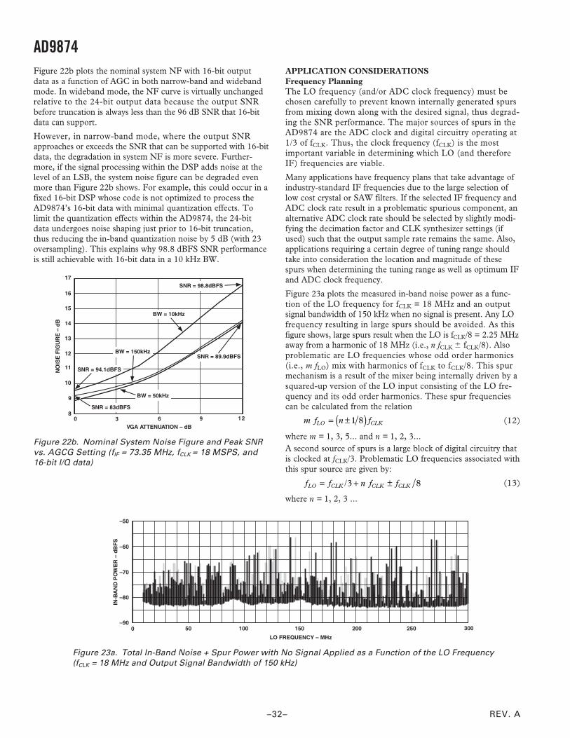
REV. A
AD9874
–32–
Figure 22b plots the nominal system NF with 16-bit outputdata as a function of AGC in both narrow-band and widebandmode. In wideband mode, the NF curve is virtually unchangedrelative to the 24-bit output data because the output SNRbefore truncation is always less than the 96 dB SNR that 16-bitdata can support.
However, in narrow-band mode, where the output SNRapproaches or exceeds the SNR that can be supported with 16-bitdata, the degradation in system NF is more severe. Further-more, if the signal processing within the DSP adds noise at thelevel of an LSB, the system noise figure can be degraded evenmore than Figure 22b shows. For example, this could occur in afixed 16-bit DSP whose code is not optimized to process theAD9874’s 16-bit data with minimal quantization effects. Tolimit the quantization effects within the AD9874, the 24-bitdata undergoes noise shaping just prior to 16-bit truncation,thus reducing the in-band quantization noise by 5 dB (with 23oversampling). This explains why 98.8 dBFS SNR performanceis still achievable with 16-bit data in a 10 kHz BW.
NO
ISE
FIG
UR
E –
dB
15
8
14
13
12
11
10
9
SNR = 98.8dBFS
BW = 50kHz
BW = 150kHz
SNR = 83dBFS
SNR = 94.1dBFS
BW = 10kHz
SNR = 89.9dBFS
16
17
3 60 9 12
VGA ATTENUATION – dB
Figure 22b. Nominal System Noise Figure and Peak SNRvs. AGCG Setting (fIF = 73.35 MHz, fCLK = 18 MSPS, and16-bit I/Q data)
APPLICATION CONSIDERATIONSFrequency PlanningThe LO frequency (and/or ADC clock frequency) must bechosen carefully to prevent known internally generated spursfrom mixing down along with the desired signal, thus degrad-ing the SNR performance. The major sources of spurs in theAD9874 are the ADC clock and digital circuitry operating at1/3 of fCLK. Thus, the clock frequency (fCLK) is the mostimportant variable in determining which LO (and thereforeIF) frequencies are viable.
Many applications have frequency plans that take advantage ofindustry-standard IF frequencies due to the large selection oflow cost crystal or SAW filters. If the selected IF frequency andADC clock rate result in a problematic spurious component, analternative ADC clock rate should be selected by slightly modi-fying the decimation factor and CLK synthesizer settings (ifused) such that the output sample rate remains the same. Also,applications requiring a certain degree of tuning range shouldtake into consideration the location and magnitude of thesespurs when determining the tuning range as well as optimum IFand ADC clock frequency.
Figure 23a plots the measured in-band noise power as a func-tion of the LO frequency for fCLK = 18 MHz and an outputsignal bandwidth of 150 kHz when no signal is present. Any LOfrequency resulting in large spurs should be avoided. As thisfigure shows, large spurs result when the LO is fCLK/8 = 2.25 MHzaway from a harmonic of 18 MHz (i.e., n fCLK fCLK/8). Alsoproblematic are LO frequencies whose odd order harmonics(i.e., m fLO) mix with harmonics of fCLK to fCLK/8. This spurmechanism is a result of the mixer being internally driven by asquared-up version of the LO input consisting of the LO fre-quency and its odd order harmonics. These spur frequenciescan be calculated from the relation
m f n fLO CLK= ±( )1 8 (12)
where m = 1, 3, 5... and n = 1, 2, 3...A second source of spurs is a large block of digital circuitry thatis clocked at fCLK/3. Problematic LO frequencies associated withthis spur source are given by:
f f n f fLO CLK CLK CLK= + ±/3 8 (13)
where n = 1, 2, 3 ...
IN-B
AN
D P
OW
ER
– d
BF
S
–60
–70
–80
–90
–50
0 250 30020015010050
LO FREQUENCY – MHz
Figure 23a. Total In-Band Noise + Spur Power with No Signal Applied as a Function of the LO Frequency(fCLK = 18 MHz and Output Signal Bandwidth of 150 kHz)
REV. A
AD9874
–33–
Figure 23b shows that omitting the LO frequencies given byEquation 12 for m = 1, 3, and 5 and by Equation 13 accountsfor most of the spurs. Some of the remaining low level spurs canbe attributed to coupling from the SSI digital output. As aresult, users are also advised to optimize the output bit rate(fCLKOUT via the SSIORD register) and the digital output driverstrength to achieve the lowest spurious and noise figure perfor-mance for a particular LO frequency and fCLK setting. This isespecially the case for particularly narrow-band channels inwhich low level spurs can degrade the AD9874’s sensitivityperformance.
Despite the many spurs, sweet spots in the LO frequency aregenerally wide enough to accommodate the maximum signalbandwidth of the AD9874. As evidence of this property, Fig-ure 24 shows that the in-band noise is quite constant for LOfrequencies ranging from 70 MHz to 71 MHz.
70.570.0
–50
–70
–60
–90
–80
71.0
LO FREQUENCY – MHz
IN-B
AN
D P
OW
ER
– d
BF
S
Figure 24. Expanded View from 70 MHz to 71 MHz
Spurious ResponsesThe spectral purity of the LO (including its phase noise) is animportant consideration since LO spurs can mix with undesiredsignals present at the AD9874’s IFIN input to produce an in-bandresponse. To demonstrate the low LO spur level introduced withinthe AD9874, Figure 25 plots the demodulated output power as afunction of the input IF frequency for an LO frequency of71.1 MHz and a clock frequency of 18 MHz.
9050
0
–40
–20
–80
–60
100
IF FREQUENCY – MHz
dB
FS
–120
–100
60 70 80
D = fCLK/4 = 4.5MHz
DESIREDRESPONSES
Figure 25. Response of AD9874 to a –20 dBm IFInput when fLO = 71.1 MHz
The two large –10 dBFS spikes near the center of the plot arethe desired responses at fLO, fIF2_ADC, where fIF2_ADC = fCLK/8,i.e., at 68.85 MHz and 73.35 MHz. LO spurs at fLO fSPUR
would result in spurious responses at offsets of fSPUR around thedesired responses. Close-in spurs of this kind are not visible onthe plot, but small spurious responses at fLO fIF2_ADC fCLK, i.e.,at 50.85 MHz, 55.35 MHz, 86.85 MHz, and 91.35 MHz, arevisible at the –90 dBFS level. This data indicates that the AD9874does an excellent job of preserving the purity of the LO signal.
Figure 25 can also be used to gauge how well the AD9874rejects undesired signals. For example, the half-IF response (at69.975 MHz and 72.225 MHz) is approximately –100 dBFS,giving a selectivity of 90 dB for this spurious response. Thelargest spurious response at approximately –70 dBFS occurswith input frequencies of 70.35 MHz and 71.85 MHz. Thesespurs result from third order nonlinearity in the signal path(i.e., abs [3 fLO – 3 fIF_Input] = fCLK/8).
IN-B
AN
D P
OW
ER
– d
BF
S
–60
–70
–80
–90
–50
0 250 300
LO FREQUENCY – MHz
20015010050
Figure 23b. Same as Figure 23a Excluding LO Frequencies Known to Produce Large In-Band Spurs
REV. A
AD9874
–34–
EXTERNAL PASSIVE COMPONENT REQUIREMENTSFigure 26 shows an example circuit using the AD9874 andTable XIV shows the nominal dc bias voltages seen at the differ-ent pins. The purpose is to show the various external passivecomponents required by the AD9874, along with nominal dcvoltages for troubleshooting purposes.
MXOP
MXON
GNDF
IF2N
IF2P
VDDFGCP
GCN
VDDA
GNDA
VREFP
VREFN
GNDL
FREF
GNDS
SYNCB
GNDH
FS
DOUTB
DOUTA
CLKOUT
VDDH
VDDD
PE
VD
DI
IFIN
CX
IF
GN
DI
CX
VL
LO
P
LO
N
CX
VM
VD
DL
VD
DP
IOU
TL
GN
DP
RR
EF
VD
DQ
IOU
TC
GN
DQ
VD
DC
GN
DC
CL
KP
CL
KN
GN
DS
GN
DD
PC
PD
48 47 46 45 44 43 42 41 40 39 38 37
13 14 15 16 17 18 19 20 21 22 23 24
1
2
3
4
5
6
7
8
9
10
11
12 25
26
27
28
29
30
31
32
33
34
35
36
AD9874
50
180pF10
H
10
H
LC
TA
NK
100pF100pF
2.2nF
100pF
10nF
100pF
100k10nF 10nF
1nF
10n
F
10n
F
100n
F
100n
F10
nF
Figure 26. Example Circuit Showing RecommendedComponent Values
Table XIV. Nominal DC Bias Voltages
Pin Number Mnemonic Nominal DC Bias (V)
1 MXOP VDDI – 0.22 MXON VDDI – 0.24 IF2N 1.3 – 1.75 IF2P 1.3 – 1.711 VREFP VDDA/2 + 0.25012 VREFN VDDA/2 – 0.25013 RREF 1.219 CLKP VDDC – 1.320 CLKN VDDC – 1.335 FREF VDDC/241 CXVM 1.6 – 2.042 LON 1.65 – 1.943 LOP 1.65 – 1.944 CXVL VDDI – 0.0546 CXIF 1.6 – 2.047 IFIN 0.9 – 1.1
The LO, CLK, and IFIN signals are coupled to their respectiveinputs using 10 nF capacitors. The output of the mixer is coupledto the input of the ADC using 100 pF. An external 100 kΩ resistorfrom the RREF pin to GND sets up the AD9874’s internal biascurrents. VREFP and VREFN provide a differential referencevoltage to the AD9874’s - ADC and must be decoupled bya 0.01 µF differential capacitor along with two 100 pF capacitors toGND. The remaining capacitors are used to decouple other sensi-tive internal nodes to GND.
Although power supply decoupling capacitors are not shown,it is recommended that a 0.1 µF surface-mount capacitor beplaced as close as possible to each power supply pin for maxi-mum effectiveness. Also not shown is the input impedancematching network used to match the AD9874’s IF input to theexternal IF filter. Lastly, the loop filter components associatedwith the LO and CLK synthesizers are not shown.
LC component values for fCLK = 18 MHz are given on the dia-gram. For other clock frequencies, the two inductors and thecapacitor of the LC tank should be scaled in inverse proportion tothe clock. For example, if fCLK = 26 MHz, then the two inductorsshould be = 6.9 µH and the capacitor should be about 120 pF. Atolerance of 10% is sufficient for these components since tuningof the LC tank is performed upon system startup.
APPLICATIONSSuperheterodyne Receiver ExampleThe AD9874 is well suited for analog and/or digital narrow-band radio systems based on a superheterodyne receiverarchitecture. The superheterodyne architecture is noted forachieving exceptional dynamic range and selectivity by usingtwo or more downconversion stages to provide amplificationof the target signal while filtering the undesired signals. TheAD9874 greatly simplifies the design of these radio systemsby integrating the complete IF strip (excluding the LO VCO)while providing an I/Q digital output (along with other systemparameters) for the demodulation of both analog and digitalmodulated signals. The AD9874’s exceptional dynamic rangeoften simplifies the IF filtering requirements and eliminates theneed for an external AGC.
Figure 27 shows a typical dual conversion superheterodynereceiver using the AD9874. An RF tuner is used to select anddownconvert the target signal to a suitable first IF for theAD9874. A preselect filter may precede the tuner to limit theRF input to the band of interest. The output of the tunerdrives an IF filter that provides partial suppression of adja-cent channels and interferers that could otherwise limit thereceiver’s dynamic range. The conversion gain of the tunershould be set such that the peak IF input signal level into theAD9874 is no greater than –18 dBm to prevent clipping. TheAD9874 downconverts the first IF signal to a second IF thatis exactly 1/8 of the - ADC’s clock rate (i.e., fCLK/8) to sim-plify the digital quadrature demodulation process.
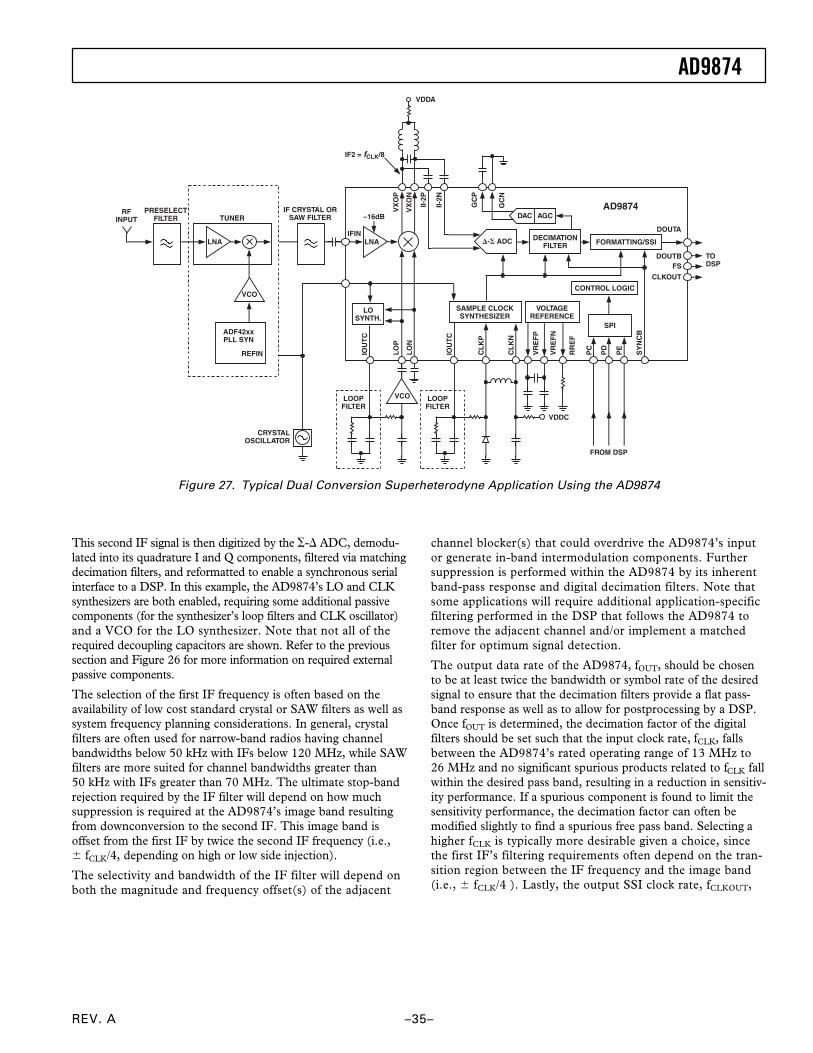
REV. A
AD9874
–35–
This second IF signal is then digitized by the - ADC, demodu-lated into its quadrature I and Q components, filtered via matchingdecimation filters, and reformatted to enable a synchronous serialinterface to a DSP. In this example, the AD9874’s LO and CLKsynthesizers are both enabled, requiring some additional passivecomponents (for the synthesizer’s loop filters and CLK oscillator)and a VCO for the LO synthesizer. Note that not all of therequired decoupling capacitors are shown. Refer to the previoussection and Figure 26 for more information on required externalpassive components.
The selection of the first IF frequency is often based on theavailability of low cost standard crystal or SAW filters as well assystem frequency planning considerations. In general, crystalfilters are often used for narrow-band radios having channelbandwidths below 50 kHz with IFs below 120 MHz, while SAWfilters are more suited for channel bandwidths greater than50 kHz with IFs greater than 70 MHz. The ultimate stop-bandrejection required by the IF filter will depend on how muchsuppression is required at the AD9874’s image band resultingfrom downconversion to the second IF. This image band isoffset from the first IF by twice the second IF frequency (i.e., fCLK/4, depending on high or low side injection).
The selectivity and bandwidth of the IF filter will depend onboth the magnitude and frequency offset(s) of the adjacent
channel blocker(s) that could overdrive the AD9874’s inputor generate in-band intermodulation components. Furthersuppression is performed within the AD9874 by its inherentband-pass response and digital decimation filters. Note thatsome applications will require additional application-specificfiltering performed in the DSP that follows the AD9874 toremove the adjacent channel and/or implement a matchedfilter for optimum signal detection.
The output data rate of the AD9874, fOUT, should be chosento be at least twice the bandwidth or symbol rate of the desiredsignal to ensure that the decimation filters provide a flat pass-band response as well as to allow for postprocessing by a DSP.Once fOUT is determined, the decimation factor of the digitalfilters should be set such that the input clock rate, fCLK, fallsbetween the AD9874’s rated operating range of 13 MHz to26 MHz and no significant spurious products related to fCLK fallwithin the desired pass band, resulting in a reduction in sensitiv-ity performance. If a spurious component is found to limit thesensitivity performance, the decimation factor can often bemodified slightly to find a spurious free pass band. Selecting ahigher fCLK is typically more desirable given a choice, sincethe first IF’s filtering requirements often depend on the tran-sition region between the IF frequency and the image band(i.e., fCLK/4 ). Lastly, the output SSI clock rate, fCLKOUT,
RFINPUT
PRESELECTFILTER TUNER
IF CRYSTAL ORSAW FILTER
VDDA
- ADCLNA
VCO
ADF42xxPLL SYN
REFIN
TODSP
AD9874
DECIMATIONFILTER
SAMPLE CLOCKSYNTHESIZER
IOU
TC
LOOPFILTER
LO
P
LO
N
VCO LOOPFILTER
VDDC
IOU
TC
CL
KP
CL
KN
FROM DSP
LOSYNTH.
VOLTAGEREFERENCE
SPI
RR
EF
VR
EF
P
VR
EF
N
SY
NC
B
PC
PD
PE
CRYSTALOSCILLATOR
IFIN
–16dB
LNA
VX
OP
VX
ON
II-2P
II-2N
DAC AGC
FORMATTING/SSI
DOUTA
DOUTBFS
CLKOUT
CONTROL LOGIC
GC
P
GC
N
IF2 = fCLK/8
Figure 27. Typical Dual Conversion Superheterodyne Application Using the AD9874
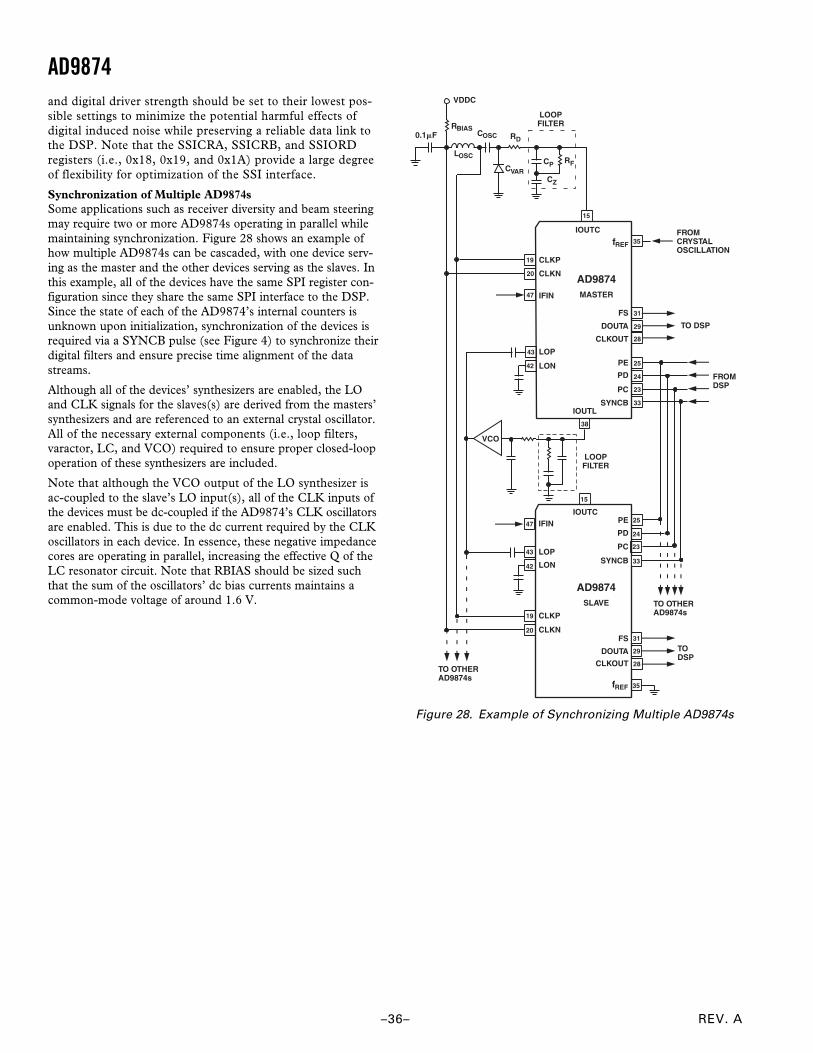
REV. A
AD9874
–36–
and digital driver strength should be set to their lowest pos-sible settings to minimize the potential harmful effects ofdigital induced noise while preserving a reliable data link tothe DSP. Note that the SSICRA, SSICRB, and SSIORDregisters (i.e., 0x18, 0x19, and 0x1A) provide a large degreeof flexibility for optimization of the SSI interface.
Synchronization of Multiple AD9874sSome applications such as receiver diversity and beam steeringmay require two or more AD9874s operating in parallel whilemaintaining synchronization. Figure 28 shows an example ofhow multiple AD9874s can be cascaded, with one device serv-ing as the master and the other devices serving as the slaves. Inthis example, all of the devices have the same SPI register con-figuration since they share the same SPI interface to the DSP.Since the state of each of the AD9874’s internal counters isunknown upon initialization, synchronization of the devices isrequired via a SYNCB pulse (see Figure 4) to synchronize theirdigital filters and ensure precise time alignment of the datastreams.
Although all of the devices’ synthesizers are enabled, the LOand CLK signals for the slaves(s) are derived from the masters’synthesizers and are referenced to an external crystal oscillator.All of the necessary external components (i.e., loop filters,varactor, LC, and VCO) required to ensure proper closed-loopoperation of these synthesizers are included.
Note that although the VCO output of the LO synthesizer isac-coupled to the slave’s LO input(s), all of the CLK inputs ofthe devices must be dc-coupled if the AD9874’s CLK oscillatorsare enabled. This is due to the dc current required by the CLKoscillators in each device. In essence, these negative impedancecores are operating in parallel, increasing the effective Q of theLC resonator circuit. Note that RBIAS should be sized suchthat the sum of the oscillators’ dc bias currents maintains acommon-mode voltage of around 1.6 V.
VCO
25
23
24
PE
PC
PD
33SYNCB
31FS
29
28
DOUTA
CLKOUT
35fREF
19
20
CLKP
CLKN
LOP
LON
43
42
IFIN47
15
AD9874MASTER
IOUTC
LOOPFILTER
38
15
IOUTC25
23
24
PE
PC
PD
35
LOP
LON
43
42
IFIN47
31FS
29
28
DOUTA
CLKOUT
33SYNCB
TODSP
CLKP
CLKN
IOUTL
TO DSP
FROMDSP
LOOPFILTER
CVAR
RD
RFCP
CZ
0.1F
LOSC
RBIASCOSC
TO OTHERAD9874s
FROMCRYSTALOSCILLATION
VDDC
TO OTHERAD9874s
AD9874SLAVE
19
20
fREF
Figure 28. Example of Synchronizing Multiple AD9874s
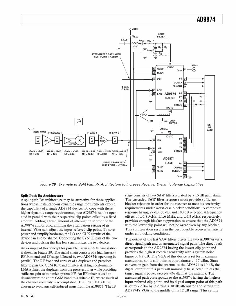
REV. A
AD9874
–37–
Split Path Rx ArchitectureA split path Rx architecture may be attractive for those applica-tions whose instantaneous dynamic range requirements exceedthe capability of a single AD9874 device. To cope with thesehigher dynamic range requirements, two AD9874s can be oper-ated in parallel with their respective clip points offset by a fixedamount. Adding a fixed amount of attenuation in front of theAD9874 and/or programming the attenuation setting of itsinternal VGA can adjust the input-referred clip point. To savepower and simplify hardware, the LO and CLK circuits of thedevice can also be shared. Connecting the SYNCB pins of the twodevices and pulsing this line low synchronizes the two devices.
An example of this concept for possible use in a GSM base stationis shown in Figure 29. The signal chain consists of a high linearityRF front end and IF stage followed by two AD9874s operating inparallel. The RF front end consists of a duplexer and preselectfilter to pass the GSM RF band of interest. A high performanceLNA isolates the duplexer from the preselect filter while providingsufficient gain to minimize system NF. An RF mixer is used todownconvert the entire GSM band to a suitable IF, where much ofthe channel selectivity is accomplished. The 170.6 MHz IF ischosen to avoid any self-induced spurs from the AD9874. The IF
stage consists of two SAW filters isolated by a 15 dB gain stage.The cascaded SAW filter response must provide sufficientblocker rejection in order for the receiver to meet its sensitivityrequirements under worst-case blocker conditions. A compositeresponse having 27 dB, 60 dB, and 100 dB rejection at frequencyoffsets of 0.8 MHz, 1.6 MHz, and 6.5 MHz, respectively,provides enough blocker suppression to ensure that the AD9874with the lower clip point will not be overdriven by any blocker.This configuration results in the best possible receiver sensitivityunder all blocking conditions.
The output of the last SAW filters drives the two AD9874s via adirect signal path and an attenuated signal path. The direct pathcorresponds to the AD9874 having the lowest clip point andprovides the highest receiver sensitivity with a system noisefigure of 4.7 dB. The VGA of this device is set for maximumattenuation, so its clip point is approximately –17 dBm. Sinceconversion gain from the antenna to the AD9874 is 19 dB, thedigital output of this path will nominally be selected unless thetarget signal’s power exceeds –36 dBm at the antenna. Theattenuated path corresponds to the AD9874 having the highestinput-referred clip point, and its digital output point of this pathis set to 7 dBm by inserting a 30 dB attenuator and setting theAD9874’s VGA to the middle of its 12 dB range. This setting
VCO
LNA XMIXER
IF SAW 1 IF SAW 2DUPLEXER PRESELECT
GAIN = –2dBNF = 2dB
GAIN = 22dBNF = 1dB
GAIN = –3dBNF = 3dB
GAIN = 5dBNF = 12dB
IFAMP
GAIN = –9dBNF = –9dB
GAIN = 15dBNF = 2dB
13MHz
DSPOR
ASIC
36dBPAD
25
23
24
PE
PC
PD
33SYNCB
31FS
29
28
DOUTA
CLKOUT
3519
20
CLKP
CLKN
LOP
LON
43
42
47
15
AD9874MASTER
LOOPFILTER
15
IOUTC25
23
24
PE
PC
PD
35
LOP
LON
43
42
IFIN47
AD9874SLAVE 31FS
29
28DOUTA
CLKOUT
33SYNCB
19
20
CLKP
CLKN
IOUTL
LOOPFILTER
CVAR
RD
RFCP
CZ
0.1F
LOSC
RBIAS
COSC
VDDC
IFIN
38
IOUTC
ATTENUATED PATH WITHCLIP POINT = 7.0dBm
DIRECT PATH WITHCLIP POINT = –17dBm
fREF
fREF
Figure 29. Example of Split Path Rx Architecture to Increase Receiver Dynamic Range Capabilities
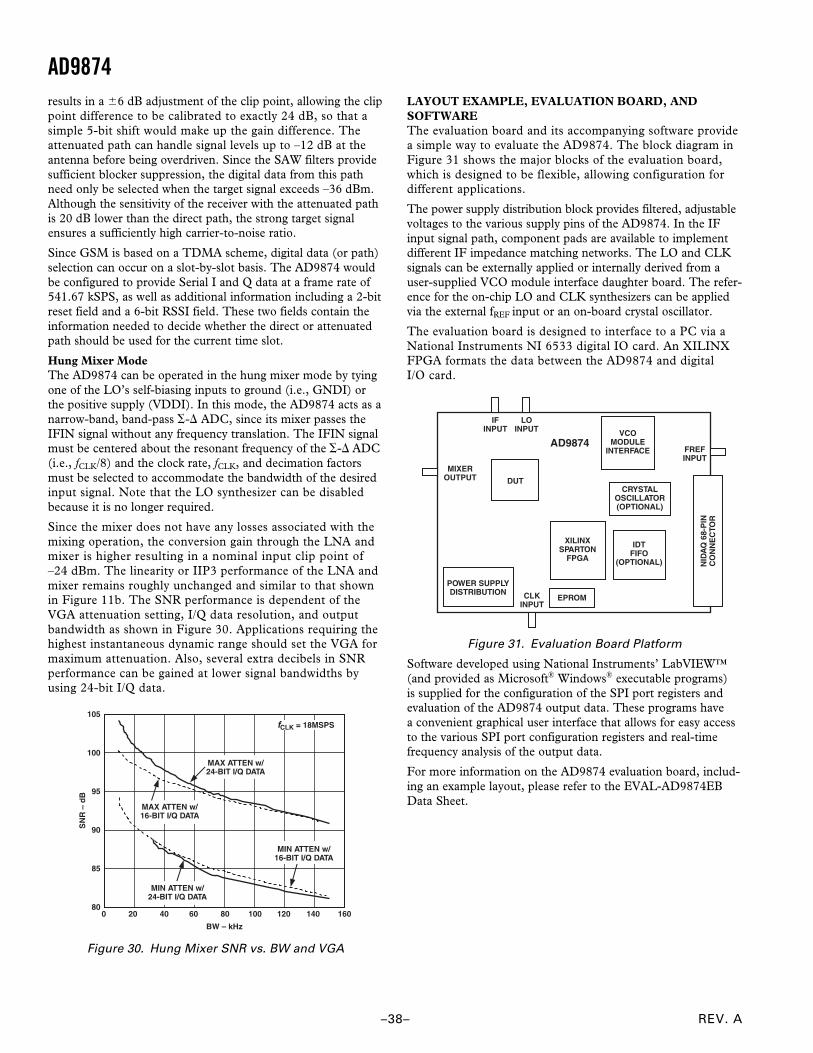
REV. A
AD9874
–38–
results in a 6 dB adjustment of the clip point, allowing the clippoint difference to be calibrated to exactly 24 dB, so that asimple 5-bit shift would make up the gain difference. Theattenuated path can handle signal levels up to –12 dB at theantenna before being overdriven. Since the SAW filters providesufficient blocker suppression, the digital data from this pathneed only be selected when the target signal exceeds –36 dBm.Although the sensitivity of the receiver with the attenuated pathis 20 dB lower than the direct path, the strong target signalensures a sufficiently high carrier-to-noise ratio.
Since GSM is based on a TDMA scheme, digital data (or path)selection can occur on a slot-by-slot basis. The AD9874 wouldbe configured to provide Serial I and Q data at a frame rate of541.67 kSPS, as well as additional information including a 2-bitreset field and a 6-bit RSSI field. These two fields contain theinformation needed to decide whether the direct or attenuatedpath should be used for the current time slot.
Hung Mixer ModeThe AD9874 can be operated in the hung mixer mode by tyingone of the LO’s self-biasing inputs to ground (i.e., GNDI) orthe positive supply (VDDI). In this mode, the AD9874 acts as anarrow-band, band-pass - ADC, since its mixer passes theIFIN signal without any frequency translation. The IFIN signalmust be centered about the resonant frequency of the - ADC(i.e., fCLK/8) and the clock rate, fCLK, and decimation factorsmust be selected to accommodate the bandwidth of the desiredinput signal. Note that the LO synthesizer can be disabledbecause it is no longer required.
Since the mixer does not have any losses associated with themixing operation, the conversion gain through the LNA andmixer is higher resulting in a nominal input clip point of–24 dBm. The linearity or IIP3 performance of the LNA andmixer remains roughly unchanged and similar to that shownin Figure 11b. The SNR performance is dependent of theVGA attenuation setting, I/Q data resolution, and outputbandwidth as shown in Figure 30. Applications requiring thehighest instantaneous dynamic range should set the VGA formaximum attenuation. Also, several extra decibels in SNRperformance can be gained at lower signal bandwidths byusing 24-bit I/Q data.
0
105
SN
R –
dB 95
BW – kHz
85
8080 120 140 1604020 60 100
100
90
MIN ATTEN w/24-BIT I/Q DATA
MAX ATTEN w/16-BIT I/Q DATA
MIN ATTEN w/16-BIT I/Q DATA
MAX ATTEN w/24-BIT I/Q DATA
fCLK = 18MSPS
Figure 30. Hung Mixer SNR vs. BW and VGA
LAYOUT EXAMPLE, EVALUATION BOARD, ANDSOFTWAREThe evaluation board and its accompanying software providea simple way to evaluate the AD9874. The block diagram inFigure 31 shows the major blocks of the evaluation board,which is designed to be flexible, allowing configuration fordifferent applications.
The power supply distribution block provides filtered, adjustablevoltages to the various supply pins of the AD9874. In the IFinput signal path, component pads are available to implementdifferent IF impedance matching networks. The LO and CLKsignals can be externally applied or internally derived from auser-supplied VCO module interface daughter board. The refer-ence for the on-chip LO and CLK synthesizers can be appliedvia the external fREF input or an on-board crystal oscillator.
The evaluation board is designed to interface to a PC via aNational Instruments NI 6533 digital IO card. An XILINXFPGA formats the data between the AD9874 and digitalI/O card.
MIXEROUTPUT DUT
IFINPUT
LOINPUT VCO
MODULEINTERFACE
CRYSTALOSCILLATOR(OPTIONAL)
IDTFIFO
(OPTIONAL)
POWER SUPPLYDISTRIBUTION
EPROMCLKINPUT
FREFINPUT
NID
AQ
68-
PIN
CO
NN
EC
TOR
XILINXSPARTON
FPGA
AD9874
Figure 31. Evaluation Board Platform
Software developed using National Instruments’ LabVIEW™(and provided as Microsoft® Windows® executable programs)is supplied for the configuration of the SPI port registers andevaluation of the AD9874 output data. These programs havea convenient graphical user interface that allows for easy accessto the various SPI port configuration registers and real-timefrequency analysis of the output data.
For more information on the AD9874 evaluation board, includ-ing an example layout, please refer to the EVAL-AD9874EBData Sheet.
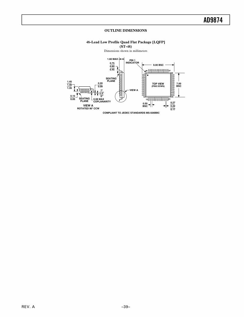
REV. A
AD9874
–39–
OUTLINE DIMENSIONS
48-Lead Low Profile Quad Flat Package [LQFP](ST-48)
Dimensions shown in millimeters
TOP VIEW(PINS DOWN)
1
1213
2524
363748
0.27 0.22 0.17
0.50BSC
7.00BSC
SEATINGPLANE
1.60 MAX
0.750.600.45
VIEW A73.50
0.20 0.09
1.45 1.40 1.35
0.150.05 0.08 MAX
COPLANARITY
VIEW AROTATED 90 CCW
PIN 1INDICATOR
9.00 BSC
COMPLIANT TO JEDEC STANDARDS MS-026BBC
SEATINGPLANE
REV. A
C02
639–
0–3/
03(A
)
AD9874
REV. A–40–
Revision HistoryLocation Page
3/03—Data sheet changed from REV. 0 to REV. A
Change to FEATURES . . . . . . . . . . . . . . . . . . . . . . . . . . . . . . . . . . . . . . . . . . . . . . . . . . . . . . . . . . . . . . . . . . . . . . . . . . . . . . . . . . . 1
Changes to FUNCTIONAL BLOCK DIAGRAM . . . . . . . . . . . . . . . . . . . . . . . . . . . . . . . . . . . . . . . . . . . . . . . . . . . . . . . . . . . . . . 1
Changes to SPECIFICATIONS . . . . . . . . . . . . . . . . . . . . . . . . . . . . . . . . . . . . . . . . . . . . . . . . . . . . . . . . . . . . . . . . . . . . . . . . . . . . 3
Changes to ORDERING GUIDE . . . . . . . . . . . . . . . . . . . . . . . . . . . . . . . . . . . . . . . . . . . . . . . . . . . . . . . . . . . . . . . . . . . . . . . . . . . 5
Replaced Figure 1b . . . . . . . . . . . . . . . . . . . . . . . . . . . . . . . . . . . . . . . . . . . . . . . . . . . . . . . . . . . . . . . . . . . . . . . . . . . . . . . . . . . . . 15
Deleted Synchronization section . . . . . . . . . . . . . . . . . . . . . . . . . . . . . . . . . . . . . . . . . . . . . . . . . . . . . . . . . . . . . . . . . . . . . . . . . . . 17
Added Synchronization Using SYNCB section . . . . . . . . . . . . . . . . . . . . . . . . . . . . . . . . . . . . . . . . . . . . . . . . . . . . . . . . . . . . . . . . 18
Changes to LO SYNTHESIZER section . . . . . . . . . . . . . . . . . . . . . . . . . . . . . . . . . . . . . . . . . . . . . . . . . . . . . . . . . . . . . . . . . . . . . 19
Changes to Figure 7b . . . . . . . . . . . . . . . . . . . . . . . . . . . . . . . . . . . . . . . . . . . . . . . . . . . . . . . . . . . . . . . . . . . . . . . . . . . . . . . . . . . 21
Changes to Figure 7c . . . . . . . . . . . . . . . . . . . . . . . . . . . . . . . . . . . . . . . . . . . . . . . . . . . . . . . . . . . . . . . . . . . . . . . . . . . . . . . . . . . . 22
Changes to Table X . . . . . . . . . . . . . . . . . . . . . . . . . . . . . . . . . . . . . . . . . . . . . . . . . . . . . . . . . . . . . . . . . . . . . . . . . . . . . . . . . . . . . 25
Changes to Automatic Gain Control section . . . . . . . . . . . . . . . . . . . . . . . . . . . . . . . . . . . . . . . . . . . . . . . . . . . . . . . . . . . . . . . . . . 29
Changes to Figure 29 . . . . . . . . . . . . . . . . . . . . . . . . . . . . . . . . . . . . . . . . . . . . . . . . . . . . . . . . . . . . . . . . . . . . . . . . . . . . . . . . . . . . 37
Changes to LAYOUT EXAMPLE, EVALUATION BOARD, and SOFTWARE section . . . . . . . . . . . . . . . . . . . . . . . . . . . . . . . . 38
Updated OUTLINE DIMENSIONS . . . . . . . . . . . . . . . . . . . . . . . . . . . . . . . . . . . . . . . . . . . . . . . . . . . . . . . . . . . . . . . . . . . . . . . 39