Embed Size (px)
DESCRIPTION
Topology for multilevel inverters to attain maximumnumber of levels from given DC sources
Citation preview
www.ietdl.org
Published in IET Power ElectronicsReceived on 6th May 2011Revised on 30th August 2011doi: 10.1049/iet-pel.2011.0178
ISSN 1755-4535
Topology for multilevel inverters to attain maximumnumber of levels from given DC sourcesK.K. Gupta S. JainDepartment of Electrical Engineering, Maulana Azad National Institute of Technology, Bhopal, IndiaE-mail: [email protected]
Abstract: This study introduces a new multilevel converter topology, which can synthesise all possible additive and subtractivecombinations of input DC levels in the output voltage waveform with fewer power electronic switches. An appropriatemodulation scheme has also been proposed for low switching frequency operation of the proposed topology. As comparedwith the classic multilevel topologies, the proposed topology results in reduction of the number of switches and conductionlosses. The operation and performance of the proposed multilevel converter has been ascertained through simulations andverified experimentally for single-phase nine-level multilevel inverter. Moreover, a 15-level inverter with asymmetric sourceconfiguration has been also investigated for charge balance control using the proposed modulation scheme. The same hasbeen verified experimentally for effective balanced power delivery.
1 Introduction
A multilevel inverter aims at synthesising a staircasewaveform with the help of appropriately connected powerswitches and multiple input DC levels. Controlled switchingof semiconductor switches plays a crucial role to achieve amultistep waveform with controllable amplitude, frequencyand phase. Such an approach to DC–AC conversion offersa number of advantages over conventional two-levelinverters, such as: capability to operate at higher voltagesusing traditional semiconductors, reduced common modevoltages, reduced dv/dt stresses, staircase waveform withbetter harmonic profile, smaller filter requirements (if any),flexibility to operate on low- and high switchingfrequencies and possibility of fault-tolerant operation [1–7].
As a result, multilevel inverters have been attracting lot ofattention in high-power and high-voltage/medium-powerapplications. Although classical multilevel topologies suchas neutral point clamped (NPC) converters [8], flyingcapacitors (FC) converters [9] and cascaded H-bridge(CHB) converters [10] have been commercialised, butdevice count becomes significantly high when they are tobe designed for increased number of voltage levels. Thisinduces complexity in implementation and increased cost.Therefore new topologies are being proposed and reportedto reduce the overall count of active and passive devices formultilevel power conversion [11–20]. However, reducingthe number of devices involves one or more of followingcompromises: increased power rating of semiconductordevices, increased number of power sources, reducednumber of redundant states and complex modulation andcontrol schemes. In spite of these compromises, thereremains a possibility of exploring topological structures
IET Power Electron., 2012, Vol. 5, Iss. 4, pp. 435–446doi: 10.1049/iet-pel.2011.0178
which can maximise the number of levels with given inputDC sources.
In this paper, a new multilevel inverter topology isproposed, which is capable of synthesising all possibleadditive and subtractive combinations of the input DClevels. Moreover, depending on the selection ofconfiguration of input DC levels, each ‘step’ in the outputwaveform so obtained is equal to the smallest input DClevel. The proposed topology bears configurational andfunctional similarity to the CHB topology in two ways:first, it needs multiple isolated input DC voltages; andsecondly, it offers the possibility of combining the inputDC voltage levels into all additive and subtractive values.An important advantage of the proposed topology over theCHB topology is in terms of conduction losses as discussedin Section 4. Subsequently, the topology can be exploredfor applications where CHB converters are effectivelyimplemented such as: grid interfacing of renewable energysources (e.g. photovoltaic) [21], static synchronouscompensators (STATCOMs) [22, 23], as multilevelbidirectional power converter for a hybrid STATCOMintegrated with energy storage systems (ESS) in distributedgeneration systems [24] and in medium voltage drivesapplications where a phase-shifting transformer withmultiple secondary windings is often employed mainly forthe reduction of line-current distortion, thus providingisolated DC sources [25].
Organisation of the paper is as follows. The proposedconcept is explained in Section 2. This section also presentsthe generalised structure of the proposed topology. InSection 3, the working of the proposed topology isexplained with the help of a nine-level inverter. Thissection also explains the proposed modulation scheme with
435
& The Institution of Engineering and Technology 2012
www.ietdl.org
low switching frequency. Simulation results are presentedalong with results of a laboratory prototype for a nine-levelinverter based on the proposed topology. A briefcomparison of the proposed topology and classicaltopologies is made in Section 4. In Section 5, the proposedtopology is further investigated for an alternate asymmetricconfiguration and charge balance control. Conclusions arepresented in Section 6.
2 Proposed topology for multilevel inverter
The proposed topology aims at synthesising all possiblecombinations that can be attained through additions andsubtractions of input DC voltage levels as described below:
1. With single DC source:If a single DC source of voltage VDCi is present, the possiblevoltage levels that can be synthesised are: +VDC1 and 0. Theresultant inverter can be a three-level or two-level inverter.Such a structure is shown in Fig. 1, which is a standardsingle-phase full-bridge inverter.2. With two DC sources:If two DC sources with voltages VDC1 and VDC2 are present,the possible combinations are
+VDC1, +VDC2, +(VDC1 − VDC2), +(VDC1 + VDC2) and 0
Thus for two DC sources, there are total nine possiblecombinations and the resulting structure should producenine levels. Such a structure is shown in Fig. 2.
Fig. 3 demonstrates the possible switch combinations toobtain the desired levels. It can be noted that three switchesconduct simultaneously for every level.3. With three DC sources:If three DC sources with voltages Vdc1, Vdc2 and Vdc3 are available,the possible combinations are: +VDC1,+VDC2,+VDC3,+(VDC1–VDC2),+ (VDC1 + VDC2), +(VDC1–VDC3), +(VDC1 +VDC3),+ (VDC2–VDC3), +(VDC2 + VDC3), +(VDC1 + VDC2 2VDC3), +(VDC1 2 VDC2 + VDC3), +(VDC1 2 VDC2 2 VDC3),+(VDC1 + VDC2 + VDC3) and 0. Thus, when three DC sourcesare present, there are 27 additive and subtractive combinationspossible including a zero level.4. With ‘k’ number of DC sources:A generalised structure is shown in Fig. 4 [26] with ‘k ’number of DC sources. If ‘k ’ number of DC sources with
Fig. 1 A full-bridge single-phase inverter
436
& The Institution of Engineering and Technology 2012
voltages VDCp, where p ¼ 1 to k, are present then theexpression for maximum number of possible levels is
Maximum number of levels =∑k
m=1
k!
m!(k − m)!2m
( )+ 1
(1)
The above expression indicates the maximum possibility insynthesising the number of levels. However, the actualnumber of levels will depend on the source configuration.Various DC source configurations and correspondingnumber of levels are discussed below:
1. ‘Unary’ configuration consists of DC sources of equalvoltages, that is
VDC1 = VDC2 = VDC3 = · · · = VDCk = VDC · · · (2)
Unary configuration is also called symmetric sourceconfiguration. Such a configuration results in (2k + 1)combinations of levels.2. ‘Binary’ configuration consists of DC sources with ageometric progression with a factor of ‘1/2’, that is
VDC1
VDC2
= VDC2
VDC3
= · · · =VDC(k−)1
VDCk
= 2 (3)
Such a configuration results in (2(k+1) 2 1) combinations oflevels.3. ‘trinary’ configuration consists of DC sources with ageometric progression with a factor of ‘1/3’ i.e.
VDC1
VDC2
= VDC2
VDC3
= · · · =VDC(k−)1
VDCk
= 3 (4)
Such a configuration results in (3k) combinations of levels.
Fig. 2 Proposed topology for nine-level output
IET Power Electron., 2012, Vol. 5, Iss. 4, pp. 435–446doi: 10.1049/iet-pel.2011.0178

www.ietdl.org
Fig. 3 Working states for nine-level inverter
IET Power Electron., 2012, Vol. 5, Iss. 4, pp. 435–446 437doi: 10.1049/iet-pel.2011.0178 & The Institution of Engineering and Technology 2012

www.ietdl.org
It can also be mentioned here that in the proposed converterwith ‘k ’ number of DC sources, the total number of switchingstates is determined as
Number of switching states = 22k (5)
3 Operating principle
In this section, the working principle of the proposed structureis explained with the help of a nine-level inverter for single-phase operation. An appropriate modulation scheme is alsopresented. The working of proposed structure is shown withthe help of simulation and verified experimentally.
3.1 Switching states to achieve requiredvoltage levels
A nine-level inverter with two DC sources VDC1 and VDC2 isshown in Fig. 2. Source configuration (unary, binary ortrinary) will decide the actual number of levels in theoutput waveform. To obtain any desired voltage level, threeswitches need to be ON simultaneously as observed fromFig. 3. There are four pairs of switches. Switch pairs (S1,S′
1) and (S4, S′4) operate complimentarily. Switch pairs (S2,
S′2) and (S3, S′
3) are not complimentary in the strict sense ofthe term but they operate in a way that the two members ofa pair cannot be ON simultaneously though they can remainOFF simultaneously. Thus, three switches (to remain ON)can be chosen from four possibilities in 4C3 (¼4) ways andeach switch has two possibilities (either ON or OFF). Thus,total number of states possible for the topology is 24 ¼ 16.All the 16 states are shown in Fig. 3 along with thecorresponding voltage output level. It can be seen that inthis single-phase configuration, the AC load is fed by ninelevels +VDC1, +VDC2, +(VDC1 – VDC2), +(VDC1 + VDC2)and ‘0’. In state 1, the switch S4
′ conducts along with S1
and S3 so that the potential difference across the load isVDC1. Similarly, an output of (VDC1–VDC2) is obtainedwhen S1, S′
3 and S4 are ON. Various redundant states canalso be noted. Voltage levels +VDC1 and +VDC2 have tworedundant states each which are (1, 2), (3, 4), (11, 12) and(13, 14), respectively. Zero level has four redundant statesviz. 7, 8, 9 and 10. All the possible states, voltage levelsand switch positions are summarised in Table 1. It isevident that asymmetry in source configuration decreasesthe number of redundant states. For example, ifVDC1 ¼ VDC2 ¼ VDC, then with reference to Table 1, theoutput levels +VDC and 0 would have increased number ofredundant states. However, irrespective of sourceconfiguration, the level +(VDC1 + VDC2) would have just
Fig. 4 Generalised structure of the proposed topology
438
& The Institution of Engineering and Technology 2012
one working state and no redundant state. This aspect limitsthe prospect of programming a fault-tolerant operationscheme with all possible output voltage levels. Fault-tolerant operation pertains to the ability of a converter toreconfigure itself so as to synthesise a given voltage level incase of power device failure(s) [27, 28] and thereforeredundant states available in a topology determine thepossibility of fault-tolerant operation.
3.2 Output voltage expressions
Corresponding to a switch Sj, let Tj be a switching function,where j ¼ {1, 2, 3, 4}, defined as
Tj = 1, if Sj is ON
0, if Sj is OFF(6)
With reference to Fig. 2, following expressions can be written
Vaa1 = −(1 − T1) · VDC1
Va1a2 = (1 − T2) · [−T ′2 · (VDC2) + T3 · (VDC1)
+ T ′3 · (VDC1 − VDC2)]
Va2b = (1 − T4)VDC2
(7)
And
Vab = Vaa1 + Va1a2 + Va2b (8)
3.3 Modulation scheme
High switching frequency modulation methods likemulticarrier pulsewidth modulation (PWM) and spacevector modulation techniques have been employed formultilevel inverter modulation control [29–31]. Also,methods such as active harmonic elimination [32], selectiveharmonic elimination (SHE) [32–34] and fundamentalfrequency method [33] are considered as low switchingfrequency methods. Any one of these methods, withsuitable adaptation, can be used for the control of proposedstructure. In this study, the control is demonstrated through
Table 1 Switching states for nine-level output
State output voltage level Switch states (1 ¼ ON, 0 ¼ OFF)
S1 S2 S3 S4 S′1 S′
2 S′3 S′
4
1 VDC1 1 0 0 0 0 0 1 1
2 VDC1 1 0 1 1 0 0 0 0
3 VDC2 0 0 1 0 1 0 0 1
4 VDC2 1 1 0 0 0 0 0 1
5 VDC1 – VDC2 1 0 0 1 0 0 1 0
6 VDC1 + VDC2 1 0 1 0 0 0 0 1
7 0 0 0 0 0 1 0 1 1
8 0 0 0 1 1 1 0 0 0
9 0 1 1 0 1 0 0 0 0
10 0 1 0 0 0 0 1 0 1
11 2VDC1 0 1 0 1 1 0 0 0
12 2VDC1 0 0 0 0 1 1 0 1
13 2VDC2 0 0 0 1 1 0 1 0
14 2VDC2 1 0 0 1 0 1 0 0
15 VDC2 – VDC1 0 1 0 0 1 0 0 1
16 2VDC1 – VDC2 0 0 0 1 1 1 0 0
IET Power Electron., 2012, Vol. 5, Iss. 4, pp. 435–446doi: 10.1049/iet-pel.2011.0178
www.ietdl.org
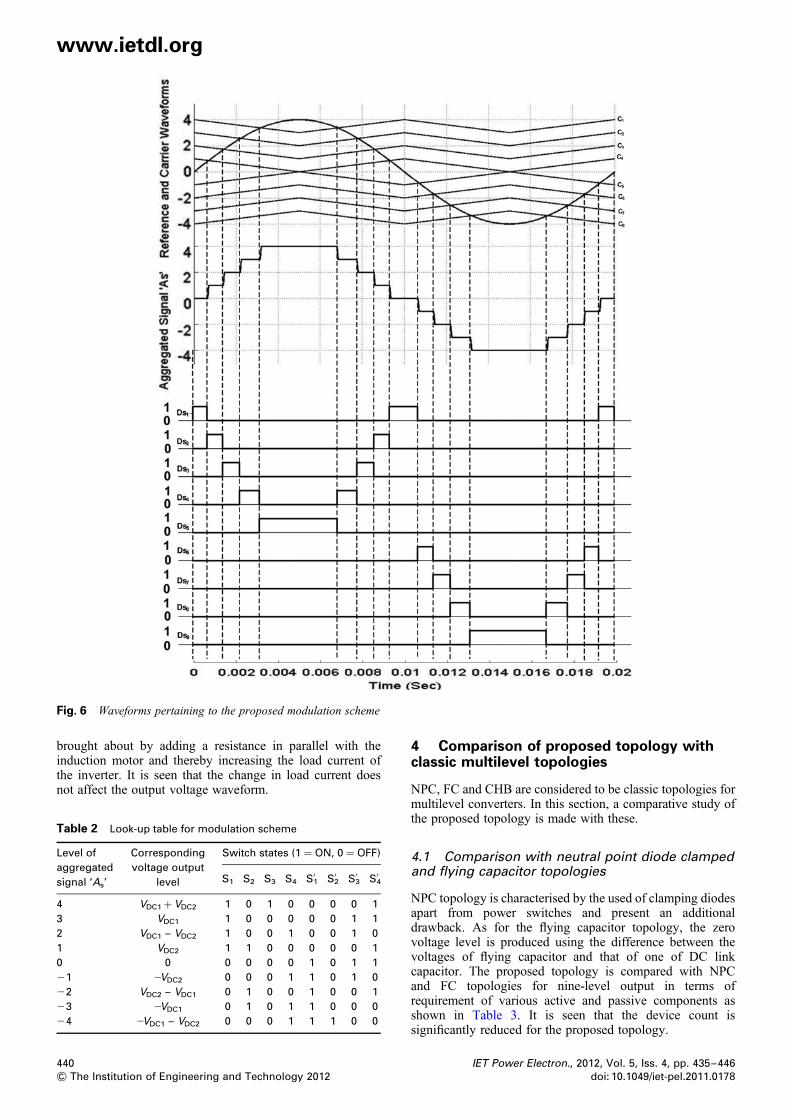
low switching frequency multicarrier PWM scheme [35, 36].In a multicarrier PWM scheme, carrier signals are comparedwith the reference signal and the pulses so obtained areused for switching of devices corresponding to therespective voltage levels [35].
The overall modulation scheme and correspondingwaveforms are shown in Figs. 5 and 6 respectively. Eighttriangular waveforms of 100 Hz frequency each are used ascarriers. A sinusoidal waveform of 50 Hz frequency is thereference signal. Carrier signals above the time-axis aredesignated as Cp, {p ¼ 1, 2, 3, 4} and those below the time-axis are designated as Cq, {q ¼ 5, 6, 7, 8}. In this scheme, ifthe reference is greater than carrier Cp, the comparatorgives ‘1’ otherwise ‘0’. If the reference is greater thancarrier Cq, the comparator gives ‘0’, otherwise ‘21’.However, in the proposed structure, various switches do notoperate independent of each other. Therefore the signalsobtained from the comparison of the carriers and referencecannot be fed directly to the switches. Therefore the signalsso obtained are aggregated so as to synthesise anaggregated signal ‘As’.
The aggregated signal ‘As’ has same number of levels asdesired in the output waveform. The switching signals arederived from this aggregated signal by comparison of thesignal with desired level and the output is fed to theswitches corresponding to the level using the lookup table,given in Table 2.
3.4 Simulation study
To examine the performance of the proposed multilevelinverter, a simulation model of single-phase nine-levelinverter is developed in MATLAB/Simulink environment.
IET Power Electron., 2012, Vol. 5, Iss. 4, pp. 435–446doi: 10.1049/iet-pel.2011.0178
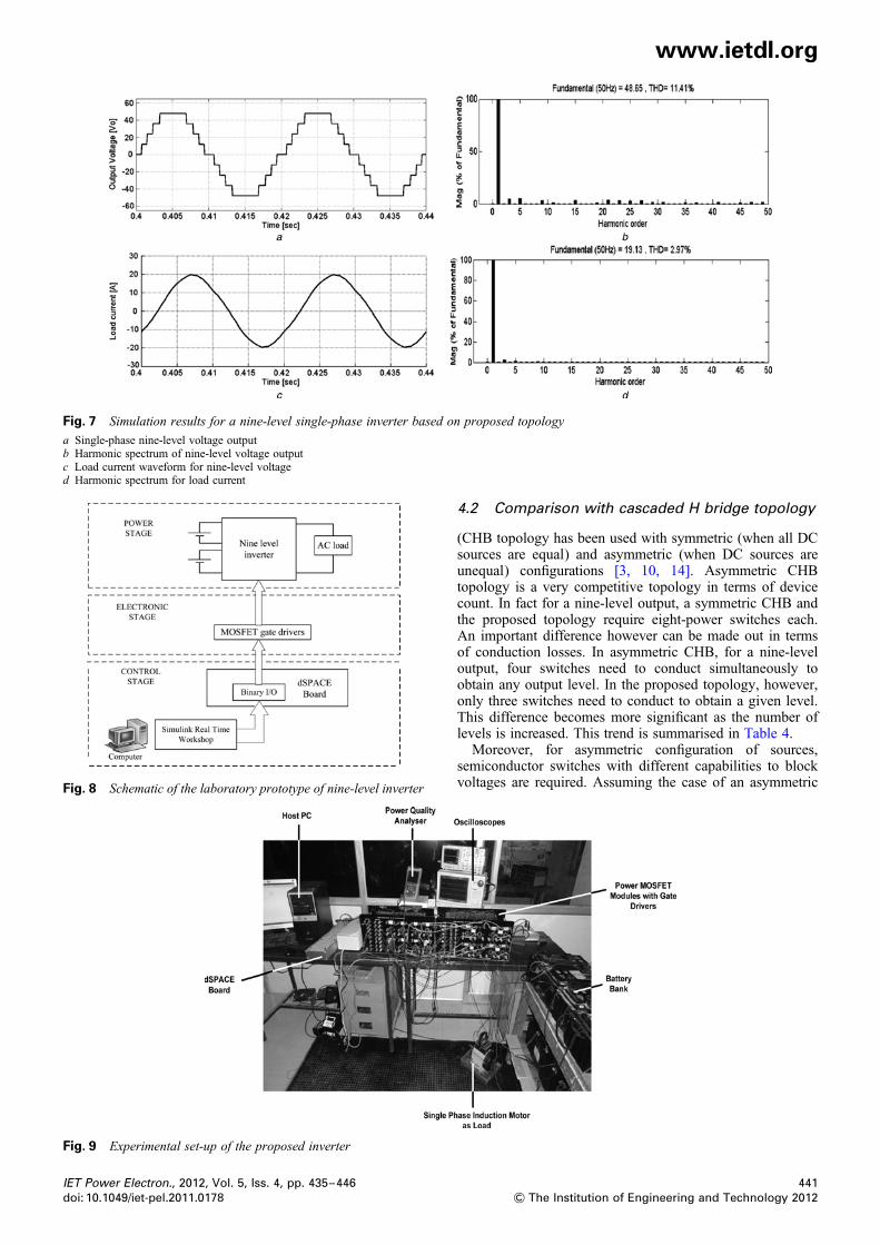
Two DC sources with VDC1 ¼ 36 V and VDC2 ¼ 12 V areused to obtain a trinary arrangement. The load is consideredto be RL load (R ¼ 2 V, L ¼ 5 mH). The inverter isoperated in open loop mode. The load voltage and currentwaveforms and their corresponding harmonic spectrum areshown in Fig. 7.
It is observed that the nine-level voltage waveform hasequal steps of 12 V each and a total harmonic distortion(THD) of 11.41%. The harmonic profile of the load voltagecan be further improved by using appropriate switchingangles [32, 33]. The load current reflects inductivebehaviour and the waveform is in close imitation ofsinusoidal shape with THD below 5% limit.
3.5 Experimental results
To validate the proposed topology, a prototype of single-phase nine-level inverter has been developed in thelaboratory. MOSFETs (IRF460) powered with suitable gatedrivers are used as switching devices. Two batteries withvoltages VDC1 ¼ 36 V and VDC ¼ 12 V are used as DCsources. dSPACE DS1103 real-time controller is used togenerate the switching pulses. A schematic diagram and theexperimental set-up of the laboratory prototype are shownin Figs. 8 and 9, respectively. A 0.5 hp single-phaseinduction motor is used as an AC load.
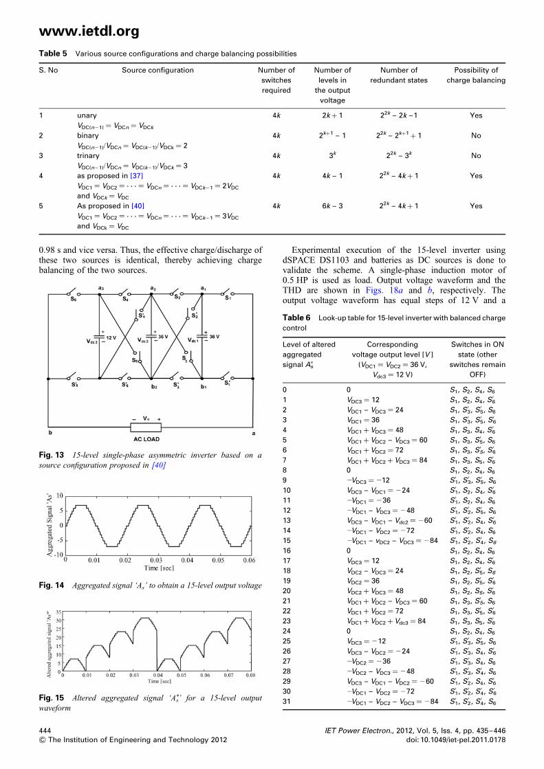
The output voltage and current waveforms are shown inFig. 10. Their respective frequency spectra are shown inFig. 11. The voltage waveform and its THD are in closeagreement with the respective simulations results. The loadvoltage is a stepped waveform of 50 Hz frequency withequal-sized steps of 12 V. The transient response is shownin Fig. 12 for a change in load. The change in load is
Fig. 5 Proposed modulation scheme for nine-level inverter
439
& The Institution of Engineering and Technology 2012
www.ietdl.org
Fig. 6 Waveforms pertaining to the proposed modulation scheme
brought about by adding a resistance in parallel with theinduction motor and thereby increasing the load current ofthe inverter. It is seen that the change in load current doesnot affect the output voltage waveform.
Table 2 Look-up table for modulation scheme
Level of
aggregated
signal ‘As’
Corresponding
voltage output
level
Switch states (1 ¼ ON, 0 ¼ OFF)
S1 S2 S3 S4 S′1 S′
2 S′3 S′
4
4 VDC1 + VDC2 1 0 1 0 0 0 0 1
3 VDC1 1 0 0 0 0 0 1 1
2 VDC1 – VDC2 1 0 0 1 0 0 1 0
1 VDC2 1 1 0 0 0 0 0 1
0 0 0 0 0 0 1 0 1 1
21 2VDC2 0 0 0 1 1 0 1 0
22 VDC2 – VDC1 0 1 0 0 1 0 0 1
23 2VDC1 0 1 0 1 1 0 0 0
24 2VDC1 – VDC2 0 0 0 1 1 1 0 0
440
& The Institution of Engineering and Technology 2012
4 Comparison of proposed topology withclassic multilevel topologies
NPC, FC and CHB are considered to be classic topologies formultilevel converters. In this section, a comparative study ofthe proposed topology is made with these.
4.1 Comparison with neutral point diode clampedand flying capacitor topologies
NPC topology is characterised by the used of clamping diodesapart from power switches and present an additionaldrawback. As for the flying capacitor topology, the zerovoltage level is produced using the difference between thevoltages of flying capacitor and that of one of DC linkcapacitor. The proposed topology is compared with NPCand FC topologies for nine-level output in terms ofrequirement of various active and passive components asshown in Table 3. It is seen that the device count issignificantly reduced for the proposed topology.
IET Power Electron., 2012, Vol. 5, Iss. 4, pp. 435–446doi: 10.1049/iet-pel.2011.0178
www.ietdl.org
4.2 Comparison with cascaded H bridge topology
(CHB topology has been used with symmetric (when all DCsources are equal) and asymmetric (when DC sources areunequal) configurations [3, 10, 14]. Asymmetric CHBtopology is a very competitive topology in terms of devicecount. In fact for a nine-level output, a symmetric CHB andthe proposed topology require eight-power switches each.An important difference however can be made out in termsof conduction losses. In asymmetric CHB, for a nine-leveloutput, four switches need to conduct simultaneously toobtain any output level. In the proposed topology, however,only three switches need to conduct to obtain a given level.This difference becomes more significant as the number oflevels is increased. This trend is summarised in Table 4.
Moreover, for asymmetric configuration of sources,semiconductor switches with different capabilities to blockvoltages are required. Assuming the case of an asymmetric
Fig. 7 Simulation results for a nine-level single-phase inverter based on proposed topology
a Single-phase nine-level voltage outputb Harmonic spectrum of nine-level voltage outputc Load current waveform for nine-level voltaged Harmonic spectrum for load current
Fig. 8 Schematic of the laboratory prototype of nine-level inverter
Fig. 9 Experimental set-up of the proposed inverter
IET Power Electron., 2012, Vol. 5, Iss. 4, pp. 435–446 441doi: 10.1049/iet-pel.2011.0178 & The Institution of Engineering and Technology 2012

www.ietdl.org
Fig. 10 Voltage and current waveforms of laboratory prototype of single-phase nine-level inverter
Fig. 11 Frequency spectra of waveforms shown in Fig. 10
a Frequency spectrum of voltage waveformb Frequency spectrum of current waveform
442
& The Institution of Engineering and Technology 2012
topology with distinct sources VDC1 and VDC2 andVDC1 . VDC2, the proposed structure would require fourswitches with minimum blocking voltage of VDC1,two switches with minimum blocking voltage of VDC2 andtwo switches with minimum blocking voltage of(VDC1 + VDC2). A CHB topology, on the other hand, wouldrequire four switches with blocking capacity of VDC1 and fourswitches with minimum voltage blocking capability of VDC2.
5 Charge balance control with asymmetricconfigurations
A multilevel inverter utilises multiple DC sources to synthesisea stepped waveform. The power drawn from the differentvoltage sources vary as a function of modulation index,output voltage levels and load power factor [37]. This mayresult in unsteady and, at times, unstable DC voltage levels.Hence the DC sources deliver unequal power. As a result,different DC sources would have different lifetimes.
This section addresses the selection of an optimalasymmetric configuration of the proposed topology with thepossibility of charge balance control. The DC sourcesbalancing in asymmetric multilevel inverters depend on theduty cycle of each level that is synthesising the desiredoutput waveforms [38]. When multiple input DC sources areused, it is desirable that these sources maintain a balancedstate of charge [39] or, in other words, exhibit equal loadsharing. Available literature indicates that though chargebalancing is achieved with symmetrical converters [37–40],it is not possible for binary and trinary configurations [38].Charge balance control can be achieved if there are two ormore input DC sources with equal voltages [38, 40].
Table 5 summarises various source configurations andcorresponding availability of redundant states, number oflevels in the output voltage and possibility of chargebalance control.
IET Power Electron., 2012, Vol. 5, Iss. 4, pp. 435–446doi: 10.1049/iet-pel.2011.0178
www.ietdl.org
Fig. 12 Waveforms depicting effect of change in load
In the light of above discussion, it can be argued that anoptimal configuration would involve a trade-off betweenasymmetry and charge balancing considerations. Babaei andHosseini [38] and Laali et al. [40] offer configurations withmore number of redundant states as compared to a binaryor trinary configuration along with possibility of chargebalancing control.
Although the proposed topology can be employed for all theconfigurations mentioned in Table 5, a source configuration
Table 3 Comparison of proposed topology with diode clamped
and flying capacitor topologies
Voltage
levels
Components Classical topologies Proposed
topologyDiode
clamped
Flying
capacitors
9 DC link capacitors 8 8 2
clamping diodes 56 – 0
clamping
capacitors
– 28 0
power switches 16 16 8
Table 4 Comparison with asymmetric CHB topology
Number of levels
in the output
voltage waveform
Number of switches conducting
simultaneously to synthesise a level
CHB topology
(with trinary
sources)
Proposed topology
(with trinary
sources)
9 4 3
27 6 4
81 8 5
243 10 6
729 12 7
IET Power Electron., 2012, Vol. 5, Iss. 4, pp. 435–446doi: 10.1049/iet-pel.2011.0178
shown in Fig. 13 is employed to demonstrate the proposedmodulation scheme for charge balance control. It has threeinput DC sources with voltages VDC1 ¼ 36 V, VDC2 ¼ 36 Vand VDC3 ¼ 12 V. Such a configuration is asymmetric andcan synthesise 15 levels in the output waveform (284 V to+84 V, in steps of 12 V each). Also, it has a total of26 ¼ 64 states, of which 53 states would be redundant(number of redundant states ¼ 22k – 4k + 1, k ¼ number ofsources ¼ 3). However, it can be emphasised that all voltagelevels possibly cannot have redundant states [37].
The fundamentals of the proposed modulation scheme asexplained in Section 3 are utilised to achieve chargebalance control in the voltage sources VDC1 and VDC2. Asper discussed in Section 3, for a 15-level voltage waveform,the obtained aggregated signal ‘As’ is shown in Fig. 14.Charge balance control can be achieved if sources VDC1 andVDC2 are utilised alternately in alternate cycles of the outputwaveform and thus balancing would be achieved in twocycles. Therefore the aggregated signal ‘As’ is altered to‘A∗
s ’ in a manner that its one cycle has four sub-parts asshown in Fig. 15. The signal has 33 levels and they areutilised as per the look-up table given in Table 6.
A 15-level asymmetric multilevel inverter based onFig. 13 is simulated using MATLAB/Simulink andSimPowerSystems toolbox. A highly inductive RL loadwith R ¼ 2 ohm and L ¼ 8 mH is considered so as toobserve the charge and discharge patterns of the DCsources. The output voltage waveform along with itsharmonic spectrum is shown in Fig. 16. It is a 15-levelstepped waveform in equal steps of 12 V. The currentwaveforms through the three DC sources are shown inFig. 17. The current waveforms of two equal DC sources(VDC1 and VDC2) indicate an alternating pattern which is aresult of swapping the two sources for voltage-levelsynthesis in alternate cycles. For example, the currentwaveform of source VDC1 in the duration t ¼ 0.94 to 0.96 sis same as that of source VDC2 in the duration t ¼ 0.96 to
443
& The Institution of Engineering and Technology 2012
www.ietdl.org
Table 5 Various source configurations and charge balancing possibilities
S. No Source configuration Number of
switches
required
Number of
levels in
the output
voltage
Number of
redundant states
Possibility of
charge balancing
1 unary 4k 2k + 1 22k – 2k –1 Yes
VDC(n21) ¼ VDCn ¼ VDCk
2 binary 4k 2k+1 – 1 22k – 2k+1 + 1 No
VDC(n21)/VDCn ¼ VDC(k21)/VDCk ¼ 2
3 trinary 4k 3k 22k – 3k No
VDC(n21)/VDCn ¼ VDC(k21)/VDCk ¼ 3
4 as proposed in [37] 4k 4k – 1 22k – 4k + 1 Yes
VDC1 ¼ VDC2 ¼ . . . ¼ VDCn ¼ . . . ¼ VDCk21 ¼ 2VDC
and VDCk ¼ VDC
5 As proposed in [40] 4k 6k – 3 22k – 4k + 1 Yes
VDC1 ¼ VDC2 ¼ . . . ¼ VDCn ¼ . . . ¼ VDCk21 ¼ 3VDC
and VDCk ¼ VDC
0.98 s and vice versa. Thus, the effective charge/discharge ofthese two sources is identical, thereby achieving chargebalancing of the two sources.
Fig. 13 15-level single-phase asymmetric inverter based on asource configuration proposed in [40]
Fig. 14 Aggregated signal ‘As’ to obtain a 15-level output voltage
Fig. 15 Altered aggregated signal ‘A∗s’ for a 15-level output
waveform
444
& The Institution of Engineering and Technology 2012
Experimental execution of the 15-level inverter usingdSPACE DS1103 and batteries as DC sources is done tovalidate the scheme. A single-phase induction motor of0.5 HP is used as load. Output voltage waveform and theTHD are shown in Figs. 18a and b, respectively. Theoutput voltage waveform has equal steps of 12 V and a
Table 6 Look-up table for 15-level inverter with balanced charge
control
Level of altered
aggregated
signal A∗s
Corresponding
voltage output level [V ]
(VDC1 ¼ VDC2 ¼ 36 V,
Vdc3 ¼ 12 V)
Switches in ON
state (other
switches remain
OFF)
0 0 S1, S2, S4, S6
1 VDC3 ¼ 12 S1, S2, S4, S′6
2 VDC1 – VDC3 ¼ 24 S1, S′3, S′
5, S6
3 VDC1 ¼ 36 S1, S′3, S′
5, S′6
4 VDC1 + VDC3 ¼ 48 S1, S3, S4, S′6
5 VDC1 + VDC2 – VDC3 ¼ 60 S1, S3, S′5, S6
6 VDC1 + VDC2 ¼ 72 S1, S3, S′5, S′
6
7 VDC1 + VDC2 + VDC3 ¼ 84 S1, S3, S5, S′6
8 0 S1, S2, S4, S6
9 2VDC3 ¼ 212 S′1, S′
3, S′5, S6
10 VDC3 – VDC1 ¼ 224 S′1, S2, S4, S′
6
11 2VDC1 ¼ 236 S′1, S2, S4, S6
12 2VDC1 – VDC3 ¼ 248 S′1, S′
2, S′5, S6
13 VDC3 – VDC1 – Vdc2 ¼ 260 S′1, S′
2, S4, S′6
14 2VDC1 – VDC2 ¼ 272 S′1, S′
2, S4, S6
15 2VDC1 – vDC2 – VDC3 ¼ 284 S′1, S′
2, S′4, S6
16 0 S1, S2, S4, S6
17 VDC3 ¼ 12 S1, S2, S4, S′6
18 VDC2 – VDC3 ¼ 24 S1, S2, S′5, S6
19 VDC2 ¼ 36 S1, S2, S′5, S′
6
20 VDC2 + VDC3 ¼ 48 S1, S2, S5, S′6
21 VDC1 + VDC2 – VDC3 ¼ 60 S1, S3, S′5, S6
22 VDC1 + VDC2 ¼ 72 S1, S3, S′5, S′
6
23 VDC1 + VDC2 + Vdc3 ¼ 84 S1, S3, S5, S′6
24 0 S1, S2, S4, S6
25 VDC3 ¼ 212 S′1, S′
3, S′5, S6
26 VDC3 – VDC2 ¼ 224 S′1, S′
3, S4, S′6
27 2VDC2 ¼ 236 S′1, S′
3, S4, S6
28 2VDC2 – VDC3 ¼ 248 S′1, S′
3, S′4, S6
29 VDC3 – VDC1 – VDC2 ¼ 260 S′1, S′
2, S4, S′6
30 2VDC1 – VDC2 ¼ 272 S′1, S′
2, S′4, S′
6
31 2VDC1 – VDC2 – VDC3 ¼ 284 S′1, S′
2, S′4, S6
IET Power Electron., 2012, Vol. 5, Iss. 4, pp. 435–446doi: 10.1049/iet-pel.2011.0178
www.ietdl.org
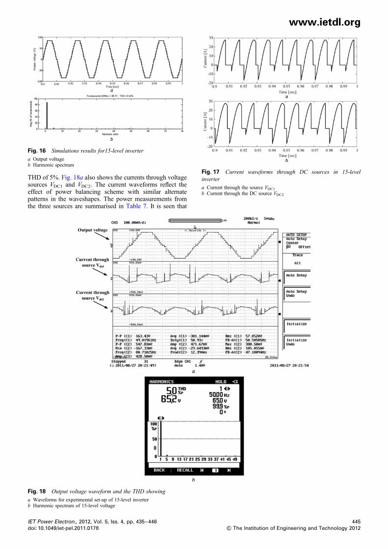
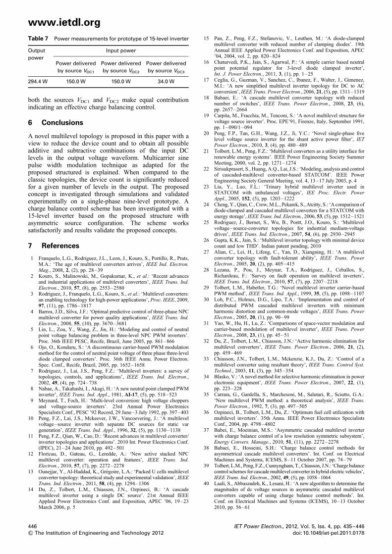
THD of 5%. Fig. 18a also shows the currents through voltagesources VDC1 and VDC2. The current waveforms reflect theeffect of power balancing scheme with similar alternatepatterns in the waveshapes. The power measurements fromthe three sources are summarised in Table 7. It is seen that
Fig. 16 Simulations results for15-level inverter
a Output voltageb Harmonic spectrum
Fig. 17 Current waveforms through DC sources in 15-levelinverter
a Current through the source VDC1
b Current through the DC source VDC2
Fig. 18 Output voltage waveform and the THD showing
a Waveforms for experimental set-up of 15-level inverterb Harmonic spectrum of 15-level voltage
IET Power Electron., 2012, Vol. 5, Iss. 4, pp. 435–446 445doi: 10.1049/iet-pel.2011.0178 & The Institution of Engineering and Technology 2012
www.ietdl.org
both the sources VDC1 and VDC2 make equal contributionindicating an effective charge balancing control.
6 Conclusions
A novel multilevel topology is proposed in this paper with aview to reduce the device count and to obtain all possibleadditive and subtractive combinations of the input DClevels in the output voltage waveform. Multicarrier sinepulse width modulation technique as adapted for theproposed structured is explained. When compared to theclassic topologies, the device count is significantly reducedfor a given number of levels in the output. The proposedconcept is investigated through simulations and validatedexperimentally on a single-phase nine-level prototype. Acharge balance control scheme has been investigated with a15-level inverter based on the proposed structure withasymmetric source configuration. The scheme workssatisfactorily and results validate the proposed concepts.
7 References
1 Franquelo, L.G., Rodriguez, J.L., Leon, J., Kouro, S., Portillo, R., Prats,M.A.: ‘The age of multilevel converters arrives’, IEEE Ind. Electron.Mag., 2008, 2, (2), pp. 28–39
2 Kouro, S., Malinowski, M., Gopakumar, K., et al.: ‘Recent advancesand industrial applications of multilevel converters’, IEEE Trans. Ind.Electron., 2010, 57, (8), pp. 2553–2580
3 Rodriguez, J., Franquelo, L.G., Kouro, S., et al.: ‘Multilevel converters:an enabling technology for high-power applications’, Proc. IEEE, 2009,97, (11), pp. 1786–1817
4 Barros, J.D., Silva, J.F.: ‘Optimal predictive control of three-phase NPCmultilevel converter for power quality applications’, IEEE Trans. Ind.Electron., 2008, 55, (10), pp. 3670–3681
5 Lin, L., Zou, Y., Wang, Z., Jin, H.: ‘Modeling and control of neutralpoint voltage balancing problem in three-level NPC PWM inverters’.Proc. 36th IEEE PESC, Recife, Brazil, June 2005, pp. 861–866
6 Ojo, O., Konduru, S.: ‘A discontinuous carrier-based PWM modulationmethod for the control of neutral point voltage of three phase three-leveldiode clamped converters’. Proc. 36th IEEE Annu. Power Electron.Spec. Conf., Recife, Brazil, 2005, pp. 1652–1658
7 Rodriguez, J., Lai, J.S., Peng, F.Z.: ‘Multilevel inverters: a survey oftopologies, controls, and applications’, IEEE Trans. Ind. Electron.,2002, 49, (4), pp. 724–738
8 Nabae, A., Takahashi, I., Akagi, H.: ‘A new neutral point clamped PWMinverter’, IEEE Trans. Ind. Appl., 1981, AI-17, (5), pp. 518–523
9 Meynard, T., Foch, H.: ‘Multi-level conversion: high voltage choppersand voltage-source inverters’. 23rd Annual Power ElectronicsSpecialists Conf., PESC ’92 Record, 29 June–3 July 1992, pp. 397–403
10 Peng, F.Z., Lai, J.S., Mckeever, J.W., Vancoevering, J.: ‘A multilevelvoltage–source inverter with separate DC sources for static vargeneration’, IEEE Trans. Ind. Appl., 1996, 32, (5), pp. 1130–1138
11 Peng, F.Z., Qian, W., Cao, D.: ‘Recent advances in multilevel converter/inverter topologies and applications’. 2010 Int. Power Electronics Conf.(IPEC), 21–24 June 2010, pp. 492–501
12 Floricau, D., Gateau, G., Leredde, A.: ‘New active stacked NPCmultilevel converter: operation and features’, IEEE Trans. Ind.Electron., 2010, 57, (7), pp. 2272–2278
13 Ounejjar, Y., Al-Haddad, K., Gregoire, L.A.: ‘Packed U cells multilevelconverter topology: theoretical study and experimental validation’, IEEETrans. Ind. Electron., 2011, 58, (4), pp. 1294–1306
14 Du, Z., Tolbert, L.M., Chiasson, J.N., Ozpineci, B.: ‘A cascademultilevel inverter using a single DC source’. 21st Annual IEEEApplied Power Electronics Conf. and Exposition, APEC ’06, 19–23March 2006, p. 5
Table 7 Power measurements for prototype of 15-level inverter
Output
power
Input power
Power delivered
by source VDC1
Power delivered
by source VDC2
Power delivered
by source VDC3
294.4 W 150.0 W 150.0 W 34.0 W
446
& The Institution of Engineering and Technology 2012
15 Pan, Z., Peng, F.Z., Stefanovic, V., Leuthen, M.: ‘A diode-clampedmultilevel converter with reduced number of clamping diodes’. 19thAnnual IEEE Applied Power Electronics Conf. and Exposition, APEC’04, 2004, vol. 2, pp. 820–824
16 Chaturvedi, P.K., Jain, S., Agarwal, P.: ‘A simple carrier based neutralpoint potential regulator for 3-level diode clamped inverter’,Int. J. Power Electron., 2011, 3, (1), pp. 1–25
17 Ceglia, G., Guzman, V., Sanchez, C., Ibanez, F., Walter, J., Gimenez,M.I.: ‘A new simplified multilevel inverter topology for DC to ACconversion’, IEEE Trans. Power Electron., 2006, 21, (5), pp. 1311–1319
18 Babaei, E.: ‘A cascade multilevel converter topology with reducednumber of switches’, IEEE Trans. Power Electron., 2008, 23, (6),pp. 2657–2664
19 Carpita, M., Fracchia, M., Tenconi, S.: ‘A novel multilevel structure forvoltage source inverter’. Proc. EPE’91, Firenze, Italy, September 1991,pp. 1–090/1–094
20 Peng, F.P., Tan, G.H., Wang, J.Z., Ji, Y.C.: ‘Novel single-phase fivelevel voltage source inverter for the shunt active power filter’, IETPower Electron., 2010, 3, (4), pp. 480–489
21 Tolbert, L.M., Peng, F.Z.: ‘Multilevel converters as a utility interface forrenewable energy systems’. IEEE Power Engineering Society SummerMeeting, 2000, vol. 2, pp. 1271–1274
22 Sirisukprasert, S., Huang, A.Q., Lai, J.S.: ‘Modeling, analysis and controlof cascaded-multilevel converter-based STATCOM’. IEEE PowerEngineering Society General Meeting, vol. 4, 13–17 July 2003, p. 4
23 Liu, Y., Luo, F.L.: ‘Trinary hybrid multilevel inverter used inSTATCOM with unbalanced voltages’, IEE Proc. Electr. PowerAppl., 2005, 152, (5), pp. 1203–1222
24 Cheng, Y., Qian, C., Crow, M.L., Pekarek, S., Atcitty, S.: ‘A comparison ofdiode-clamped and cascaded multilevel converters for a STATCOM withenergy storage’, IEEE Trans. Ind. Electron., 2006, 53, (5), pp. 1512–1521
25 Rodriguez, J., Bernet, S., Wu, B., Pontt, J.O., Kouro, S.: ‘Multilevelvoltage–source-converter topologies for industrial medium-voltagedrives’, IEEE Trans. Ind. Electron., 2007, 54, (6), pp. 2930–2945
26 Gupta, K.K., Jain, S.: ‘Multilevel inverter topology with minimal devicecount and low THD’. Indian patent pending, 2010
27 Alian, C., Lei, H., Lifeng, C., Yan, D., Xiangning, H.: ‘A multilevelconverter topology with fault-tolerant ability’, IEEE Trans. PowerElectron., 2005, 20, (2), pp. 405–415
28 Lezana, P., Pou, J., Meynar, T.A., Rodriguez, J., Ceballos, S.,Richardeau, F.: ‘Survey on fault operation on multilevel inverters’,IEEE Trans. Ind. Electron., 2010, 57, (7), pp. 2207–2218
29 Tolbert, L.M., Habetler, T.G.: ‘Novel multilevel inverter carrier-basedPWM method’, IEEE Trans. Ind. Appl., 1999, 35, (5), pp. 1098–1107
30 Loh, P.C., Holmes, D.G., Lipo, T.A.: ‘Implementation and control ofdistributed PWM cascaded multilevel inverters with minimumharmonic distortion and common-mode voltages’, IEEE Trans. PowerElectron., 2005, 20, (1), pp. 90–99
31 Yao, W., Hu, H., Lu, Z.: ‘Comparisons of space-vector modulation andcarrier-based modulation of multilevel inverter’, IEEE Trans. PowerElectron., 2008, 23, (1), pp. 45–51
32 Du, Z., Tolbert, L.M., Chiasson, J.N.: ‘Active harmonic elimination formultilevel converters’, IEEE Trans. Power Electron., 2006, 21, (2),pp. 459–469
33 Chiasson, J.N., Tolbert, L.M., Mckenzie, K.J., Du, Z.: ‘Control of amultilevel converter using resultant theory’, IEEE Trans. Control Syst.Technol., 2003, 11, (3), pp. 345–354
34 Blasko, V.: ‘A novel method for selective harmonic elimination in powerelectronic equipment’, IEEE Trans. Power Electron., 2007, 22, (1),pp. 223–228
35 Carrara, G., Gardella, S., Marchesoni, M., Salutari, R., Sciutto, G.A.:‘New multilevel PWM method: a theoretical analysis’, IEEE Trans.Power Electron., 1992, 7, (3), pp. 497–505
36 Ozpineci, B., Tolbert, L.M., Du, Z.: ‘Optimum fuel cell utilization withmultilevel inverters’. 35th Annu. IEEE Power Electronics SpecialistsConf., 2004, pp. 4798–4802
37 Babei, E., Moeinian, M.S.: ‘Asymmetric cascaded multilevel inverterwith charge balance control of a low resolution symmetric subsystem’,Energy Convers. Manage., 2010, 51, (11), pp. 2272–2278
38 Babaei, E., Hosseini, S.H.: ‘Charge balance control methods forasymmetrical cascade multilevel converters’. Int. Conf. on ElectricalMachines and Systems, ICEMS, 8–11 October 2007, pp. 74–79
39 Tolbert, L.M., Peng, F.Z., Cunnyngham, T., Chiasson, J.N.: ‘Charge balancecontrol schemes for cascade multilevel converter in hybrid electric vehicles’,IEEE Trans. Ind. Electron., 2002, 49, (5), pp. 1058–1064
40 Laali, S., Abbaszadeh, K., Lesani, H.: ‘A new algorithm to determine themagnitudes of dc voltage sources in asymmetric cascaded multilevelconverters capable of using charge balance control methods’. Int.Conf. on Electrical Machines and Systems (ICEMS), 10–13 October2010, pp. 56–61
IET Power Electron., 2012, Vol. 5, Iss. 4, pp. 435–446doi: 10.1049/iet-pel.2011.0178


![Cascaded Multilevel Inverters with Reduced Structures ... › article_964_e9d67543741c53cc... · structure and the ease of extending to higher voltage levels [3]. Cascaded multilevel](https://img.pdfslide.us/doc/110x75/5f0f86d27e708231d4449a23/cascaded-multilevel-inverters-with-reduced-structures-a-article964e9d67543741c53cc.jpg)


![Type-1 and Type-2 Fuzzy Logic Controller Based Multilevel ... · types of multilevel inverters: cascaded H-bridge, diode clamped, flying capacitors [6]. The advantages of multilevel](https://img.pdfslide.us/doc/110x75/5f0b60b77e708231d43038d2/type-1-and-type-2-fuzzy-logic-controller-based-multilevel-types-of-multilevel.jpg)