Embed Size (px)
Citation preview
This article has been accepted for inclusion in a future issue of this journal. Content is final as presented, with the exception of pagination.
IEEE TRANSACTIONS ON VERY LARGE SCALE INTEGRATION (VLSI) SYSTEMS 1
A Low-Power DSP for Wireless CommunicationsHyunseok Lee, Member, IEEE, Chaitali Chakrabarti, Senior Member, IEEE, and Trevor Mudge, Fellow, IEEE
Abstract—This paper proposes a low-power high-throughputdigital signal processor (DSP) for baseband processing in wirelessterminals. It builds on our earlier architecture—Signal processingOn Demand Architecture (SODA)—which is a four-processor,32-lane SIMD machine that was optimized for WCDMA 2 Mbpsand IEEE 802.11a. SODA has several shortcomings includinglarge register file power, wasted cycles for data alignment, etc.,and cannot satisfy the higher throughput and lower power re-quirements of emerging standards. We propose SODA-II, whichaddresses these problems by deploying the following schemes:operation chaining, pipelined execution of SIMD units, staggeredmemory access, and multicycling of computation units. Operationchaining involves chaining the primitive instructions, therebyeliminating unnecessary register file accesses and saving power.Pipelined execution of the vector instructions through the SIMDunits improves the system throughput. Staggered execution ofcomputation units helps simplify the data alignment networks.It is implemented in conjunction with multicycling so that thecomputation units are busy most of the time. The proposed archi-tecture is evaluated with an in-house architecture emulator whichuses component-level area and power models built with Synopsysand Artisan tools. Our results show that for WCDMA 2 Mbps,the proposed architecture uses two processors and consumes only120 mW while SODA uses four processors and consumes 210 mWwhen implemented in 0.13- m technology and clocked at 300MHz.
Index Terms—Baseband processor, digital signal processing(DP), low power, programmable, SIMD, software-defined radio(SDR).
I. INTRODUCTION
R ECENT years have seen an emergence of a large numberof protocols that please see query in Mudge bio cater to
different types of wireless communication networks. In theseprotocols, baseband processing is one of the most computa-tionally demanding parts and is usually realized with ASICsfor power efficiency. But ASIC-based hardwired solutions arecostly because of the large number of existing and upcomingwireless standards. Software-defined radio (SDR) providesa cost-effective and flexible solution for implementing mul-tiple wireless protocols in software. In this paper, we present aprogrammable, high-throughput, low-power processor for base-band processing. Designing such a processor is challenging,because programmability is usually achieved at the cost ofenergy efficiency.
Manuscript received September 18, 2008; revised May 14, 2009.H. Lee is with the Department of Electronics and Communications
Engineering, Kwangwoon University, 139-701 Seoul, Korea (e-mail: [email protected]).
C. Chakrabarti is with the Department of Electrical Engineering, ArizonaState University, Tempe, AZ 85287-5706 USA (e-mail: [email protected]).
T. Mudge is with the Department of Electrical Engineering and ComputerScience, University of Michigan, Ann Arbor, MI 48105-2122 USA (e-mail:[email protected]).
Digital Object Identifier 10.1109/TVLSI.2009.2023547
Several programmable architectures have been proposed forbaseband processing that achieve high energy efficiency byexploiting the inherent parallelism in many of the algorithms.Data-level parallelism (DLP) has been exploited efficientlyin a number of the existing SIMD-based architectures suchas Infineon’s MUSIC [1], Analog Devices’ TigerSHARC [2],Icera’s DXP [3], NXP’s EVP [4], SandBridge’s SandBlaster[5], Linköping’s SIMT [6], and Michigan’s SODA [7]. Therealso exists some degree of thread-level parallelism (TLP) whichhas been supported by SandBlaster [5], SIMT [6], and SODA[7]. In addition, there are heterogeneous SDR architecturesthat support fine-grained parallelism such as PicoArray [8]and XiRisc [9], or coarse-grain parallelism such as Intel RCA[10], QuickSilver [11], Montium [12], and ADRES [13]. Inthis paper we present a programmable baseband processor,SODA-II, that takes advantage of the inherent parallelism innovel ways to further increase energy efficiency for current andemerging standards.
Previously we developed a low-power programmable multi-processor architecture, Signal processing On Demand Architec-ture (SODA) [7], for supporting wireless baseband processingprotocols such as W-CDMA 2 Mbps [14] and IEEE 802.11a[15]. Each processor consists of a 16-bit and 32-lane SIMDdatapath to handle the vector computations, a scalar datapath,scratch pad memories, address generation unit, and DMA sup-port. The main drawbacks of SODA are that it spends a signifi-cant amount of time on noncomputational operations such as re-aligning data through a shuffle network and performing a largenumber of register file accesses. This is quite typical of wideSIMD architectures, and similar observations have been madein [16] and [17].
In order to design the next generation of low-power signalprocessors with higher throughput and lower power, we need toreevaluate the interaction between algorithms and architecture.Our analysis of the workload characteristics of the wirelessprotocols revealed that the majority of baseband processingis implemented by the following vector algorithm kernels:finite impulse response (FIR) filters, pattern matching, min-imum/maximum finding, fast Fourier transforms (FFT), andthe Viterbi operations of branch metric computation (BMC)and add-compare-select (ACS). These kernels can be furtherdecomposed into five primitive vector operations of data load,vector alignment, vector computation, vector reduction, anddata store. These characteristics guided the design of theproposed architecture, SODA-II. While SODA-II retained themultiprocessor wide SIMD architecture of SODA, it signifi-cantly improved upon the performance and energy efficiencyof SODA by employing the following schemes, namely, oper-ation chaining, pipelined execution of SIMD units, staggeredmemory access, and multicycling in computation units. Oper-ation chaining involves chaining the primitive instructions andimproves the throughput and power performance by reducing
1063-8210/$26.00 © 2009 IEEE
Authorized licensed use limited to: Arizona State University. Downloaded on December 16, 2009 at 10:35 from IEEE Xplore. Restrictions apply.
This article has been accepted for inclusion in a future issue of this journal. Content is final as presented, with the exception of pagination.
2 IEEE TRANSACTIONS ON VERY LARGE SCALE INTEGRATION (VLSI) SYSTEMS
TABLE IMAJOR ALGORITHM KERNELS IN THE BASEBAND PROCESSING WORKLOAD
the number of register file accesses. Pipelined execution ofSIMD units supports parallel execution of vector operations andincreases the system throughput. It is efficient for vector algo-rithm kernels with simple data alignment patterns such as FIRfilter, pattern matching, and min/max finding. For algorithmsthat have complex data alignment and require multiple cyclesfor computation such as FFT and Viterbi, a combination ofstaggered memory access and multicycling of the computationunits results in lower power and higher throughput.
To evaluate the effectiveness of these schemes, we imple-mented a hardware model of SODA-II. At the component level,we used Verilog and Synopsys’ Physical Compiler for charac-terization and used PrimePower to generate power estimates.The component-level information was used in an architectureemulation program to generate kernel-level and system-levelpower estimates. We compared the performance of the proposedarchitecture with the original SODA [7], termed the referencearchitecture in this paper. We found that operation chainingand pipelined execution of SIMD units improved the systemthroughput the most, and operation chaining and staggeredmemory accesses enhanced the system energy efficiency themost. As an application example, we showed that for WCDMA2-Mbps packet service, the proposed architecture requirestwo processors (PEs) and consumes an estimated 120 mWcompared to SODA which requires four PEs and consumes anestimated 210 mW when implemented in 0.13- m technologyand clocked at 300 MHz.
The rest of the paper is organized as follows. Section IIbriefly describes the key characteristics of the wireless pro-tocols. Section III describes the limitations of SODA andthen proposes three architectural schemes to improve its per-formance. Section IV describes the details of the SODA-IIarchitecture. Section V provides an analysis of its power andthroughput performance. Section VI includes a brief surveyof existing baseband processor architectures. Section VII con-cludes with some remarks.
II. WORKLOAD CHARACTERIZATION
There are three main categories of wireless communicationsystems. These are based on time division multiple access(TDMA), code division multiple access (CDMA), and orthog-onal frequency division multiple access (OFDMA). Despite thedifferences in their mode of operation, baseband processing
TABLE IIDISTRIBUTION OF WORKLOAD FOR THE 2-Mbps WCDMA PACKET
DATA SERVICE. THE VECTOR ALGORITHMS CONSTITUTE
MORE THAN 90% OF THE TOTAL WORKLOAD
shows many common characteristics: 1) the number of majoralgorithm kernels is few; 2) baseband operation is a mixtureof vector and sequential algorithm kernels; 3) vector algorithmkernels dominate baseband workload; and 4) vector algorithmkernels can be decomposed into five primitive vector oper-ations. We elaborate on these characteristics and show howthey are exploited in the development of the proposed DSParchitecture.
Table I shows that the majority of baseband processingcan be modeled as a combination of five vector algorithmkernels and eight scalar algorithm kernels. The five vectorkernels are FIR filtering, pattern matching, min/max finding,Viterbi-BMC/ACS, and FFT, and the eight scalar kernels areViterbi-TB (trace-back), interleaving, symbol mapping, channelencoding, sliding window, code generation, interpolation, andfrequency tracking.
An analysis of the wireless protocols shows that the vectorkernels account for more than 90% of the baseband processingworkload of protocols based on TDMA, CDMA, or OFDMA.Thus, the power efficiency and throughput of a baseband pro-cessor is determined by how efficiently the vector kernels canbe computed. As an example, Table II shows the distributionof workload for the 2-Mbps WCDMA packet data servicebefore parallelizing. To avoid diverging from the main themeof the paper, the detailed workload characterization for the2-Mbps WCDMA packet data service has been included in theAppendix.
Further analysis showed that the vector algorithm kernelscan be decomposed into five vector operations: data load,vector alignment, computation, vector reduction, and datastore. Table III summarizes the decomposition of the fivevector kernels. Data load involves reading input operands frommemory; vector alignment shuffles or permutes the loadeddata before or after vector computation; vector computationperforms arithmetic or logical operations in parallel; vectorreduction converts the output of the vector computation into a
Authorized licensed use limited to: Arizona State University. Downloaded on December 16, 2009 at 10:35 from IEEE Xplore. Restrictions apply.
This article has been accepted for inclusion in a future issue of this journal. Content is final as presented, with the exception of pagination.
LEE et al.: A LOW-POWER DSP FOR WIRELESS COMMUNICATIONS 3
TABLE IIIDECOMPOSITION OF MAJOR VECTOR ALGORITHM KERNELS INTO FIVE VECTOR OPERATIONS
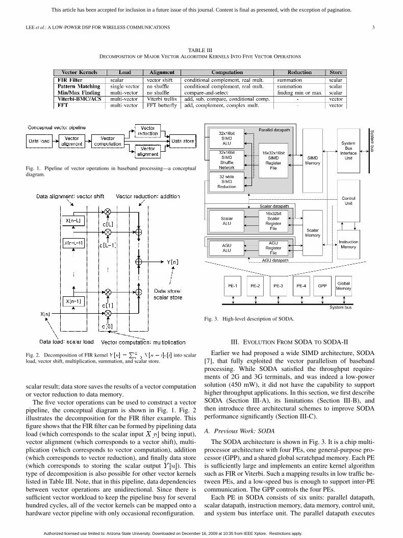
Fig. 1. Pipeline of vector operations in baseband processing—a conceptualdiagram.
Fig. 2. Decomposition of FIR kernel � ��� � ��� � ������ into scalarload, vector shift, multiplication, summation, and scalar store.
scalar result; data store saves the results of a vector computationor vector reduction to data memory.
The five vector operations can be used to construct a vectorpipeline, the conceptual diagram is shown in Fig. 1. Fig. 2illustrates the decomposition for the FIR filter example. Thisfigure shows that the FIR filter can be formed by pipelining dataload (which corresponds to the scalar input being input),vector alignment (which corresponds to a vector shift), multi-plication (which corresponds to vector computation), addition(which corresponds to vector reduction), and finally data store(which corresponds to storing the scalar output ). Thistype of decomposition is also possible for other vector kernelslisted in Table III. Note, that in this pipeline, data dependenciesbetween vector operations are unidirectional. Since there issufficient vector workload to keep the pipeline busy for severalhundred cycles, all of the vector kernels can be mapped onto ahardware vector pipeline with only occasional reconfiguration.
Fig. 3. High-level description of SODA.
III. EVOLUTION FROM SODA TO SODA-II
Earlier we had proposed a wide SIMD architecture, SODA[7], that fully exploited the vector parallelism of basebandprocessing. While SODA satisfied the throughput require-ments of 2G and 3G terminals, and was indeed a low-powersolution (450 mW), it did not have the capability to supporthigher throughput applications. In this section, we first describeSODA (Section III-A), its limitations (Section III-B), andthen introduce three architectural schemes to improve SODAperformance significantly (Section III-C).
A. Previous Work: SODA
The SODA architecture is shown in Fig. 3. It is a chip multi-processor architecture with four PEs, one general-purpose pro-cessor (GPP), and a shared global scratchpad memory. Each PEis sufficiently large and implements an entire kernel algorithmsuch as FIR or Viterbi. Such a mapping results in low traffic be-tween PEs, and a low-speed bus is enough to support inter-PEcommunication. The GPP controls the four PEs.
Each PE in SODA consists of six units: parallel datapath,scalar datapath, instruction memory, data memory, control unit,and system bus interface unit. The parallel datapath executes
Authorized licensed use limited to: Arizona State University. Downloaded on December 16, 2009 at 10:35 from IEEE Xplore. Restrictions apply.
This article has been accepted for inclusion in a future issue of this journal. Content is final as presented, with the exception of pagination.
4 IEEE TRANSACTIONS ON VERY LARGE SCALE INTEGRATION (VLSI) SYSTEMS
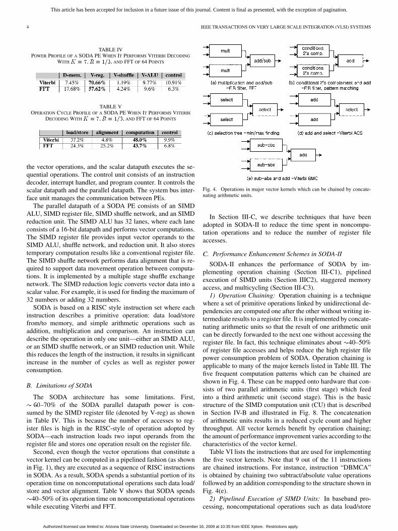
TABLE IVPOWER PROFILE OF A SODA PE WHEN IT PERFORMS VITERBI DECODING
WITH � � �, � � ���, AND FFT OF 64 POINTS
TABLE VOPERATION CYCLE PROFILE OF A SODA PE WHEN IT PERFORMS VITERBI
DECODING WITH � � �, � � ���, AND FFT OF 64 POINTS
the vector operations, and the scalar datapath executes the se-quential operations. The control unit consists of an instructiondecoder, interrupt handler, and program counter. It controls thescalar datapath and the parallel datapath. The system bus inter-face unit manages the communication between PEs.
The parallel datapath of a SODA PE consists of an SIMDALU, SIMD register file, SIMD shuffle network, and an SIMDreduction unit. The SIMD ALU has 32 lanes, where each laneconsists of a 16-bit datapath and performs vector computations.The SIMD register file provides input vector operands to theSIMD ALU, shuffle network, and reduction unit. It also storestemporary computation results like a conventional register file.The SIMD shuffle network performs data alignment that is re-quired to support data movement operation between computa-tions. It is implemented by a multiple stage shuffle exchangenetwork. The SIMD reduction logic converts vector data into ascalar value. For example, it is used for finding the maximum of32 numbers or adding 32 numbers.
SODA is based on a RISC style instruction set where eachinstruction describes a primitive operation: data load/storefrom/to memory, and simple arithmetic operations such asaddition, multiplication and comparison. An instruction candescribe the operation in only one unit—either an SIMD ALU,or an SIMD shuffle network, or an SIMD reduction unit. Whilethis reduces the length of the instruction, it results in significantincrease in the number of cycles as well as register powerconsumption.
B. Limitations of SODA
The SODA architecture has some limitations. First,–70% of the SODA parallel datapath power is con-
sumed by the SIMD register file (denoted by V-reg) as shownin Table IV. This is because the number of accesses to reg-ister files is high in the RISC-style of operation adopted bySODA—each instruction loads two input operands from theregister file and stores one operation result on the register file.
Second, even though the vector operations that constitute avector kernel can be computed in a pipelined fashion (as shownin Fig. 1), they are executed as a sequence of RISC instructionsin SODA. As a result, SODA spends a substantial portion of itsoperation time on noncomputational operations such data load/store and vector alignment. Table V shows that SODA spends
40–50% of its operation time on noncomputational operationswhile executing Viterbi and FFT.
Fig. 4. Operations in major vector kernels which can be chained by concate-nating arithmetic units.
In Section III-C, we describe techniques that have beenadopted in SODA-II to reduce the time spent in noncompu-tation operations and to reduce the number of register fileaccesses.
C. Performance Enhancement Schemes in SODA-II
SODA-II enhances the performance of SODA by im-plementing operation chaining (Section III-C1), pipelinedexecution of SIMD units (Section IIIC2), staggered memoryaccess, and multicycling (Section III-C3).
1) Operation Chaining: Operation chaining is a techniquewhere a set of primitive operations linked by unidirectional de-pendencies are computed one after the other without writing in-termediate results to a register file. It is implemented by concate-nating arithmetic units so that the result of one arithmetic unitcan be directly forwarded to the next one without accessing theregister file. In fact, this technique eliminates about 40–50%of register file accesses and helps reduce the high register filepower consumption problem of SODA. Operation chaining isapplicable to many of the major kernels listed in Table III. Thefive frequent computation patterns which can be chained areshown in Fig. 4. These can be mapped onto hardware that con-sists of two parallel arithmetic units (first stage) which feedinto a third arithmetic unit (second stage). This is the basicstructure of the SIMD computation unit (CU) that is describedin Section IV-B and illustrated in Fig. 8. The concatenationof arithmetic units results in a reduced cycle count and higherthroughput. All vector kernels benefit by operation chaining;the amount of performance improvement varies according to thecharacteristics of the vector kernel.
Table VI lists the instructions that are used for implementingthe five vector kernels. Note that 9 out of the 11 instructionsare chained instructions. For instance, instruction “DBMCA”is obtained by chaining two subtract/absolute value operationsfollowed by an addition corresponding to the structure shown inFig. 4(e).
2) Pipelined Execution of SIMD Units: In baseband pro-cessing, noncomputational operations such as data load/store
Authorized licensed use limited to: Arizona State University. Downloaded on December 16, 2009 at 10:35 from IEEE Xplore. Restrictions apply.

This article has been accepted for inclusion in a future issue of this journal. Content is final as presented, with the exception of pagination.
LEE et al.: A LOW-POWER DSP FOR WIRELESS COMMUNICATIONS 5
TABLE VICHAINED AND PRIMITIVE INSTRUCTIONS USED FOR IMPLEMENTING THE VECTOR KERNELS
Fig. 5. Mapping of conceptual vector pipeline onto a pipeline of SIMD execu-tion units.
and vector alignment occupy a substantial portion of the totalcycle count (see Table V). So significant gain can be achievedif the vector operations can be executed in a pipelined fashionresulting in reduced number of load/store and alignmentoperations.
Fig. 5 shows the mapping of the vector operations onto apipeline of SIMD execution units. The data dependencies be-tween the vector operations are unidirectional, and so there isno complex data forwarding between the corresponding hard-ware units. The net result is a significant reduction in the numberof data load/store instructions. For this scheme to be effective,the pipeline has to be highly utilized. Our workload analysisshows that the vector kernel algorithms keep the pipeline busyfor long periods of time, resulting in significant performanceenhancement.
The pipelined execution scheme is certainly an efficient wayof implementing vector kernels with simple data alignment pat-terns such as FIR filtering, min/max finding, etc. However, itsapplication to vector kernels with complex data alignment andmulticycle computations (such as Viterbi and FFT) results infunction unit underutilization and the use of power-hungry data
Fig. 6. Execution of computation units using (a) SIMD mode and (b) staggeredmode.
alignment networks. In Section III-C3, we describe how to al-leviate these problems by using a combination of staggered ex-ecution of computation units and multicycling.
3) Staggered Memory Access and Multicycling in Computa-tion Units: As mentioned earlier, data alignment is fairly simplefor FIR filtering, pattern matching, and min/max finding. For in-stance, for FIR filtering, one scalar element can be read from thedata memory and shifted into the vector registers. As a result, avector load from data memory can be avoided. For kernels withcomplex data alignment such as Viterbi and FFT, vector load canbe avoided by distributing data in multiple memory banks. How-ever the data have to be aligned using switches beforethe data can be fed to the computation units. In an architecturethat supports operation chaining, four sets of switcheswould be required, resulting in a fairly large area overhead.
Now, if the operations in the SIMD computation unit could bestaggered, as in time division multiplexing, then eachswitch could be replaced with a single switch. The dataalignment problem could now be handled by the memory ad-dress generators. Fig. 6 illustrates the SIMD mode and staggeredmode of operation in a datapath with four computation units. Formore details, please refer to [18].
One potential problem with such a design is that in manycases, the computation unit is underutilized. If the architecturehas 16 computation units, then the computation unit has to have
Authorized licensed use limited to: Arizona State University. Downloaded on December 16, 2009 at 10:35 from IEEE Xplore. Restrictions apply.
This article has been accepted for inclusion in a future issue of this journal. Content is final as presented, with the exception of pagination.
6 IEEE TRANSACTIONS ON VERY LARGE SCALE INTEGRATION (VLSI) SYSTEMS
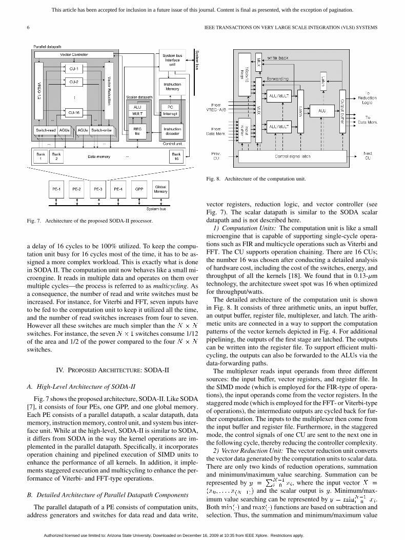
Fig. 7. Architecture of the proposed SODA-II processor.
a delay of 16 cycles to be 100% utilized. To keep the compu-tation unit busy for 16 cycles most of the time, it has to be as-signed a more complex workload. This is exactly what is donein SODA II. The computation unit now behaves like a small mi-croengine. It reads in multiple data and operates on them overmultiple cycles—the process is referred to as multicycling. Asa consequence, the number of read and write switches must beincreased. For instance, for Viterbi and FFT, seven inputs haveto be fed to the computation unit to keep it utilized all the time,and the number of read switches increases from four to seven.However all these switches are much simpler than theswitches. For instance, the seven switches consume 1/12of the area and 1/2 of the power compared to the fourswitches.
IV. PROPOSED ARCHITECTURE: SODA-II
A. High-Level Architecture of SODA-II
Fig. 7 shows the proposed architecture, SODA-II. Like SODA[7], it consists of four PEs, one GPP, and one global memory.Each PE consists of a parallel datapath, a scalar datapath, datamemory, instruction memory, control unit, and system bus inter-face unit. While at the high-level, SODA-II is similar to SODA,it differs from SODA in the way the kernel operations are im-plemented in the parallel datapath. Specifically, it incorporatesoperation chaining and pipelined execution of SIMD units toenhance the performance of all kernels. In addition, it imple-ments staggered execution and multicycling to enhance the per-formance of Viterbi- and FFT-type operations.
B. Detailed Architecture of Parallel Datapath Components
The parallel datapath of a PE consists of computation units,address generators and switches for data read and data write,
Fig. 8. Architecture of the computation unit.
vector registers, reduction logic, and vector controller (seeFig. 7). The scalar datapath is similar to the SODA scalardatapath and is not described here.
1) Computation Units: The computation unit is like a smallmicroengine that is capable of supporting single-cycle opera-tions such as FIR and multicycle operations such as Viterbi andFFT. The CU supports operation chaining. There are 16 CUs;the number 16 was chosen after conducting a detailed analysisof hardware cost, including the cost of the switches, energy, andthroughput of all the kernels [18]. We found that in 0.13- mtechnology, the architecture sweet spot was 16 when optimizedfor throughput/watts.
The detailed architecture of the computation unit is shownin Fig. 8. It consists of three arithmetic units, an input buffer,an output buffer, register file, multiplexer, and latch. The arith-metic units are connected in a way to support the computationpatterns of the vector kernels depicted in Fig. 4. For additionalpipelining, the outputs of the first stage are latched. The outputscan be written into the register file. To support efficient multi-cycling, the outputs can also be forwarded to the ALUs via thedata-forwarding paths.
The multiplexer reads input operands from three differentsources: the input buffer, vector registers, and register file. Inthe SIMD mode (which is employed for the FIR-type of opera-tions), the input operands come from the vector registers. In thestaggered mode (which is employed for the FFT- or Viterbi-typeof operations), the intermediate outputs are cycled back for fur-ther computation. The inputs to the multiplexer then come fromthe input buffer and register file. Furthermore, in the staggeredmode, the control signals of one CU are sent to the next one inthe following cycle, thereby reducing the controller complexity.
2) Vector Reduction Unit: The vector reduction unit convertsthe vector data generated by the computation units to scalar data.There are only two kinds of reduction operations, summationand minimum/maximum value searching. Summation can berepresented by , where the input vector
and the scalar output is . Minimum/max-imum value searching can be represented by .Both and functions are based on subtraction andselection. Thus, the summation and minimum/maximum value
Authorized licensed use limited to: Arizona State University. Downloaded on December 16, 2009 at 10:35 from IEEE Xplore. Restrictions apply.
This article has been accepted for inclusion in a future issue of this journal. Content is final as presented, with the exception of pagination.
LEE et al.: A LOW-POWER DSP FOR WIRELESS COMMUNICATIONS 7
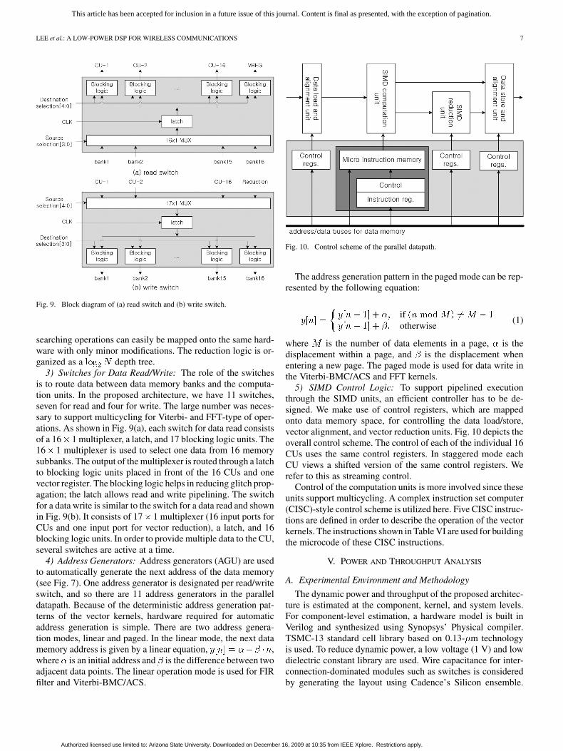
Fig. 9. Block diagram of (a) read switch and (b) write switch.
searching operations can easily be mapped onto the same hard-ware with only minor modifications. The reduction logic is or-ganized as a depth tree.
3) Switches for Data Read/Write: The role of the switchesis to route data between data memory banks and the computa-tion units. In the proposed architecture, we have 11 switches,seven for read and four for write. The large number was neces-sary to support multicycling for Viterbi- and FFT-type of oper-ations. As shown in Fig. 9(a), each switch for data read consistsof a 16 1 multiplexer, a latch, and 17 blocking logic units. The16 1 multiplexer is used to select one data from 16 memorysubbanks. The output of the multiplexer is routed through a latchto blocking logic units placed in front of the 16 CUs and onevector register. The blocking logic helps in reducing glitch prop-agation; the latch allows read and write pipelining. The switchfor a data write is similar to the switch for a data read and shownin Fig. 9(b). It consists of 17 1 multiplexer (16 input ports forCUs and one input port for vector reduction), a latch, and 16blocking logic units. In order to provide multiple data to the CU,several switches are active at a time.
4) Address Generators: Address generators (AGU) are usedto automatically generate the next address of the data memory(see Fig. 7). One address generator is designated per read/writeswitch, and so there are 11 address generators in the paralleldatapath. Because of the deterministic address generation pat-terns of the vector kernels, hardware required for automaticaddress generation is simple. There are two address genera-tion modes, linear and paged. In the linear mode, the next datamemory address is given by a linear equation, ,where is an initial address and is the difference between twoadjacent data points. The linear operation mode is used for FIRfilter and Viterbi-BMC/ACS.
Fig. 10. Control scheme of the parallel datapath.
The address generation pattern in the paged mode can be rep-resented by the following equation:
ifotherwise
(1)
where is the number of data elements in a page, is thedisplacement within a page, and is the displacement whenentering a new page. The paged mode is used for data write inthe Viterbi-BMC/ACS and FFT kernels.
5) SIMD Control Logic: To support pipelined executionthrough the SIMD units, an efficient controller has to be de-signed. We make use of control registers, which are mappedonto data memory space, for controlling the data load/store,vector alignment, and vector reduction units. Fig. 10 depicts theoverall control scheme. The control of each of the individual 16CUs uses the same control registers. In staggered mode eachCU views a shifted version of the same control registers. Werefer to this as streaming control.
Control of the computation units is more involved since theseunits support multicycling. A complex instruction set computer(CISC)-style control scheme is utilized here. Five CISC instruc-tions are defined in order to describe the operation of the vectorkernels. The instructions shown in Table VI are used for buildingthe microcode of these CISC instructions.
V. POWER AND THROUGHPUT ANALYSIS
A. Experimental Environment and Methodology
The dynamic power and throughput of the proposed architec-ture is estimated at the component, kernel, and system levels.For component-level estimation, a hardware model is built inVerilog and synthesized using Synopsys’ Physical compiler.TSMC-13 standard cell library based on 0.13- m technologyis used. To reduce dynamic power, a low voltage (1 V) and lowdielectric constant library are used. Wire capacitance for inter-connection-dominated modules such as switches is consideredby generating the layout using Cadence’s Silicon ensemble.
Authorized licensed use limited to: Arizona State University. Downloaded on December 16, 2009 at 10:35 from IEEE Xplore. Restrictions apply.
This article has been accepted for inclusion in a future issue of this journal. Content is final as presented, with the exception of pagination.
8 IEEE TRANSACTIONS ON VERY LARGE SCALE INTEGRATION (VLSI) SYSTEMS
TABLE VIICOMPONENT-LEVEL BREAKDOWN OF THE POWER CONSUMPTION AND AREA
OF SODA-II. THE AVERAGE POWER IS FOR THE WCDMA 2-MbpsPACKET
DATA SERVICE WHEN ONLY TWO PES ARE ACTIVE. THE LEAKAGE POWER
AND AREA CORRESPOND TO THE FOUR-PROCESSOR ARCHITECTURE
Additionally, Artisan’s memory compiler is used for the gener-ation of storage components. The memory compiler providesHDL models which are used for generating the timing andpower information. The gate-level dynamic power is evaluatedusing Synopsys’ PrimePower. Overall, the component-levelpower estimates are fairly accurate.
The kernel-level power estimates are obtained by using thecomponent-level models in an architecture emulation programthat was developed in house. The emulation program calculatesthe activity level of each component during the execution ofthe assembly program. This is used to estimate the cycle countand power consumption of each kernel. In order to consider theeffect of global clocking and interconnection, we assume 30%power and area overhead. Finally, the system-level throughputand power estimate is calculated by aggregating kernel-level es-timation. We expect our estimates to be within 20% of those ob-tained by fully synthesized designs.
All comparisons are with respect to the reference architec-ture, SODA. Since SODA was implemented in 0.18- m tech-nology, operated at 1.8 V, and was clocked at 400 MHz, it wasresynthesized using the same parameters as the proposed ar-chitecture, namely, 0.13- m technology, 1 V, low-K material,and 300-MHz operation frequency. The operation frequency of300 MHz was chosen by evaluating the energy/cycle versus op-eration frequency (in the range 100–800 MHz) for WCDMA2 Mbps and then choosing the frequency with the lowest en-ergy/cycle.
B. Component-Level Analysis of SODA-II
1) Power: Table VII shows the component-level powerbreakdown of SODA-II. The average power is the powerconsumed while executing WCDMA 2-Mbps packet dataservice by only two PEs; the other two PEs are inactive.From Table VII, we see that the data memory and instruction
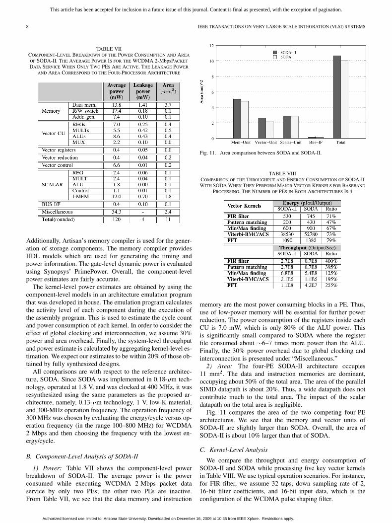
Fig. 11. Area comparison between SODA and SODA-II.
TABLE VIIICOMPARISON OF THE THROUGHPUT AND ENERGY CONSUMPTION OF SODA-IIWITH SODA WHEN THEY PERFORM MAJOR VECTOR KERNELS FOR BASEBAND
PROCESSING. THE NUMBER OF PES IN BOTH ARCHITECTURES IS 4
memory are the most power consuming blocks in a PE. Thus,use of low-power memory will be essential for further powerreduction. The power consumption of the registers inside eachCU is 7.0 mW, which is only 80% of the ALU power. Thisis significantly small compared to SODA where the registerfile consumed about 6–7 times more power than the ALU.Finally, the 30% power overhead due to global clocking andinterconnection is presented under “Miscellaneous.”
2) Area: The four-PE SODA-II architecture occupies11 mm . The data and instruction memories are dominant,occupying about 50% of the total area. The area of the parallelSIMD datapath is about 20%. Thus, a wide datapath does notcontribute much to the total area. The impact of the scalardatapath on the total area is negligible.
Fig. 11 compares the area of the two competing four-PEarchitectures. We see that the memory and vector units ofSODA-II are slightly larger than SODA. Overall, the area ofSODA-II is about 10% larger than that of SODA.
C. Kernel-Level Analysis
We compare the throughput and energy consumption ofSODA-II and SODA while processing five key vector kernelsin Table VIII. We use typical operation scenarios. For instance,for FIR filter, we assume 32 taps, down sampling rate of 2,16-bit filter coefficients, and 16-bit input data, which is theconfiguration of the WCDMA pulse shaping filter.
Authorized licensed use limited to: Arizona State University. Downloaded on December 16, 2009 at 10:35 from IEEE Xplore. Restrictions apply.

This article has been accepted for inclusion in a future issue of this journal. Content is final as presented, with the exception of pagination.
LEE et al.: A LOW-POWER DSP FOR WIRELESS COMMUNICATIONS 9
TABLE IXPOWER COMPARISON BETWEEN THE REFERENCE ARCHITECTURE
(4 PES) AND THE PROPOSED ARCHITECTURE (2 PES)FOR WCDMA 2-Mbps PACKET DATA SERVICE
Table VIII shows that SODA-II consumes about 20–50%less energy than SODA. Most of the energy savings comefrom the following factors. The first is the use of operationchaining, which minimizes the number of power-consumingregister file accesses. The second is the low control overheadbecause there is no additional decoding after the initial config-uration—streaming control is used to coordinate the pipelinedexecution in each SIMD lane and across lanes. The third isthe simplified data alignment where the switches arereplaced with switches during staggered mode operation.
Table VIII also shows that SODA-II processes about 1.3–4times more input data than SODA. This is primarily because ofoperation chaining and pipelined execution of SIMD units. Theperformance of the min/max finding kernel is not as impressive.Here the data load takes comparatively more time and does notutilize pipelined execution through the SIMD units effectively.
D. System-Level Analysis: WCDMA 2-Mbps Workload
For processing WCDMA2-Mbps packet data workload,SODA utilizes all four PEs and consumes 210 mW whileSODA-II utilizes only two PEs and consumes 120 mW. Incomparison, the SB3010 processor from Sandbridge, which isimplemented in 90 nm, consumes 600 mW, which is signifi-cantly higher compared to both SODA and SODA-II.
Table IX compares the power performance of SODA andSODA-II. The column “memory” represents the power dissi-pated for data load/store from/to memory. The column “vectorcomputation” represents the power for vector computations thatincludes the power consumption of arithmetic units and registerfiles. The column “scalar” represents the power consumption forthe scalar workload. The column “vector control” represents thepower dissipated for vector control signal generation. The twoarchitectures show identical power consumption for system businterface and scalar workloads.
From Table IX, we see that SODA-II dissipates less powerfor the vector computations and the vector control signal gener-ation. The reduction in the vector computation power is becauseof operation chaining. The reduction in the control signal gen-eration power is because control instructions are not decoded inevery cycle and the control signals flow in a streaming fashion.While accessing memory, the proposed architecture dissipatesmore energy than SODA. This is because the data load/store op-erations are performed through switches which are power con-suming. However, the power gains of the vector computationand vector control generation operations more than compensatefor this overhead.
Fig. 12. Impact of three schemes on system throughput (bits per second) andenergy cost (Joules per bit).
E. Impact of Three Schemes
In order to analyze the impact of the three schemes, westudied five system configurations with respect to both max-imum throughput and energy cost, represented by energyconsumption per bit: A) reference architecture SODA, B)SODA with operation chaining; C) SODA with pipelinedexecution of SIMD units referred to as SIMD pipelining; D)SODA with operation chaining and SIMD pipelining; and E)SODA with operation chaining, SIMD pipelining, staggeredexecution and multicycling (SODA-II). For evaluation, webuild kernel-level and system-level models corresponding to allconfigurations. Fig. 12 illustrates the impact of each of theseschemes.
We see that operation chaining (configuration B) improvessystem throughput by about 70% and reduces energy cost byabout 20% by decreasing the number of data load/store instruc-tions and thus the number of register file accesses. Pipelinedexecution of SIMD units (configuration C) increases the systemthroughput by about 140% because multiple vector operationscan now be processed at the same time. Vector kernels withsimple data alignment patterns such as FIR filter, patternmatching, min-max can be processed very efficiently becauseof this enhancement. The energy cost, however, increases byabout 15% due to more complex control that is required to
Authorized licensed use limited to: Arizona State University. Downloaded on December 16, 2009 at 10:35 from IEEE Xplore. Restrictions apply.
This article has been accepted for inclusion in a future issue of this journal. Content is final as presented, with the exception of pagination.
10 IEEE TRANSACTIONS ON VERY LARGE SCALE INTEGRATION (VLSI) SYSTEMS
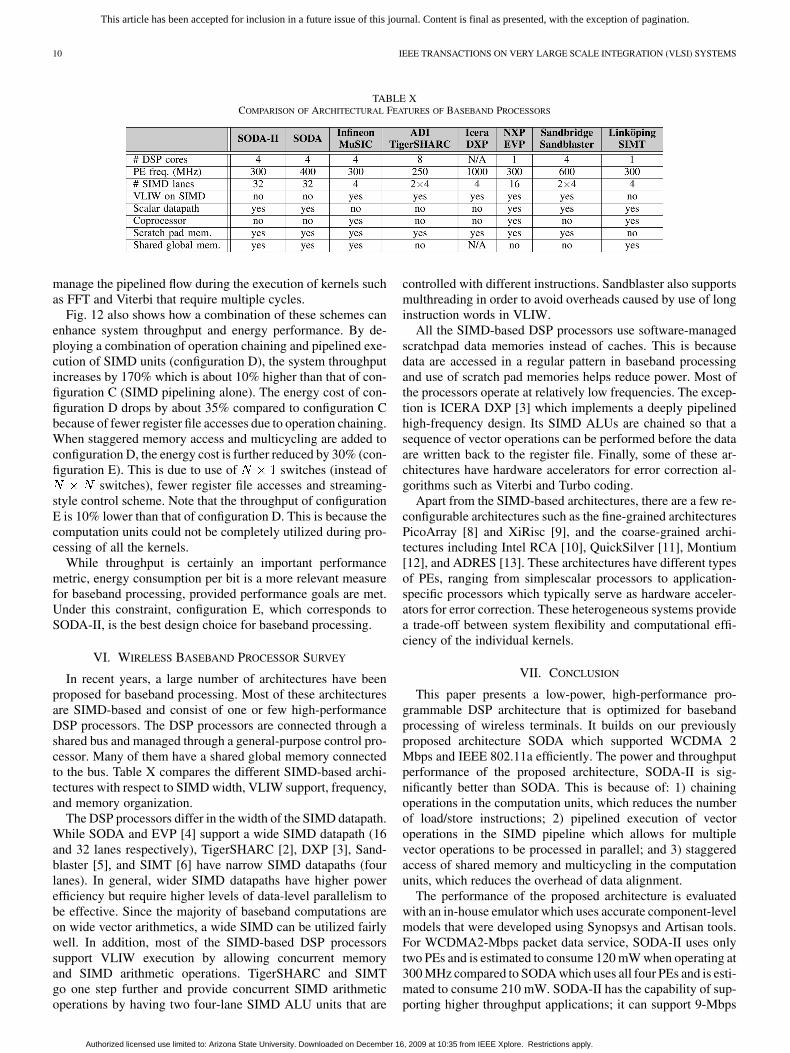
TABLE XCOMPARISON OF ARCHITECTURAL FEATURES OF BASEBAND PROCESSORS
manage the pipelined flow during the execution of kernels suchas FFT and Viterbi that require multiple cycles.
Fig. 12 also shows how a combination of these schemes canenhance system throughput and energy performance. By de-ploying a combination of operation chaining and pipelined exe-cution of SIMD units (configuration D), the system throughputincreases by 170% which is about 10% higher than that of con-figuration C (SIMD pipelining alone). The energy cost of con-figuration D drops by about 35% compared to configuration Cbecause of fewer register file accesses due to operation chaining.When staggered memory access and multicycling are added toconfiguration D, the energy cost is further reduced by 30% (con-figuration E). This is due to use of switches (instead of
switches), fewer register file accesses and streaming-style control scheme. Note that the throughput of configurationE is 10% lower than that of configuration D. This is because thecomputation units could not be completely utilized during pro-cessing of all the kernels.
While throughput is certainly an important performancemetric, energy consumption per bit is a more relevant measurefor baseband processing, provided performance goals are met.Under this constraint, configuration E, which corresponds toSODA-II, is the best design choice for baseband processing.
VI. WIRELESS BASEBAND PROCESSOR SURVEY
In recent years, a large number of architectures have beenproposed for baseband processing. Most of these architecturesare SIMD-based and consist of one or few high-performanceDSP processors. The DSP processors are connected through ashared bus and managed through a general-purpose control pro-cessor. Many of them have a shared global memory connectedto the bus. Table X compares the different SIMD-based archi-tectures with respect to SIMD width, VLIW support, frequency,and memory organization.
The DSP processors differ in the width of the SIMD datapath.While SODA and EVP [4] support a wide SIMD datapath (16and 32 lanes respectively), TigerSHARC [2], DXP [3], Sand-blaster [5], and SIMT [6] have narrow SIMD datapaths (fourlanes). In general, wider SIMD datapaths have higher powerefficiency but require higher levels of data-level parallelism tobe effective. Since the majority of baseband computations areon wide vector arithmetics, a wide SIMD can be utilized fairlywell. In addition, most of the SIMD-based DSP processorssupport VLIW execution by allowing concurrent memoryand SIMD arithmetic operations. TigerSHARC and SIMTgo one step further and provide concurrent SIMD arithmeticoperations by having two four-lane SIMD ALU units that are
controlled with different instructions. Sandblaster also supportsmulthreading in order to avoid overheads caused by use of longinstruction words in VLIW.
All the SIMD-based DSP processors use software-managedscratchpad data memories instead of caches. This is becausedata are accessed in a regular pattern in baseband processingand use of scratch pad memories helps reduce power. Most ofthe processors operate at relatively low frequencies. The excep-tion is ICERA DXP [3] which implements a deeply pipelinedhigh-frequency design. Its SIMD ALUs are chained so that asequence of vector operations can be performed before the dataare written back to the register file. Finally, some of these ar-chitectures have hardware accelerators for error correction al-gorithms such as Viterbi and Turbo coding.
Apart from the SIMD-based architectures, there are a few re-configurable architectures such as the fine-grained architecturesPicoArray [8] and XiRisc [9], and the coarse-grained archi-tectures including Intel RCA [10], QuickSilver [11], Montium[12], and ADRES [13]. These architectures have different typesof PEs, ranging from simplescalar processors to application-specific processors which typically serve as hardware acceler-ators for error correction. These heterogeneous systems providea trade-off between system flexibility and computational effi-ciency of the individual kernels.
VII. CONCLUSION
This paper presents a low-power, high-performance pro-grammable DSP architecture that is optimized for basebandprocessing of wireless terminals. It builds on our previouslyproposed architecture SODA which supported WCDMA 2Mbps and IEEE 802.11a efficiently. The power and throughputperformance of the proposed architecture, SODA-II is sig-nificantly better than SODA. This is because of: 1) chainingoperations in the computation units, which reduces the numberof load/store instructions; 2) pipelined execution of vectoroperations in the SIMD pipeline which allows for multiplevector operations to be processed in parallel; and 3) staggeredaccess of shared memory and multicycling in the computationunits, which reduces the overhead of data alignment.
The performance of the proposed architecture is evaluatedwith an in-house emulator which uses accurate component-levelmodels that were developed using Synopsys and Artisan tools.For WCDMA2-Mbps packet data service, SODA-II uses onlytwo PEs and is estimated to consume 120 mW when operating at300 MHz compared to SODA which uses all four PEs and is esti-mated to consume 210 mW. SODA-II has the capability of sup-porting higher throughput applications; it can support 9-Mbps
Authorized licensed use limited to: Arizona State University. Downloaded on December 16, 2009 at 10:35 from IEEE Xplore. Restrictions apply.
This article has been accepted for inclusion in a future issue of this journal. Content is final as presented, with the exception of pagination.
LEE et al.: A LOW-POWER DSP FOR WIRELESS COMMUNICATIONS 11
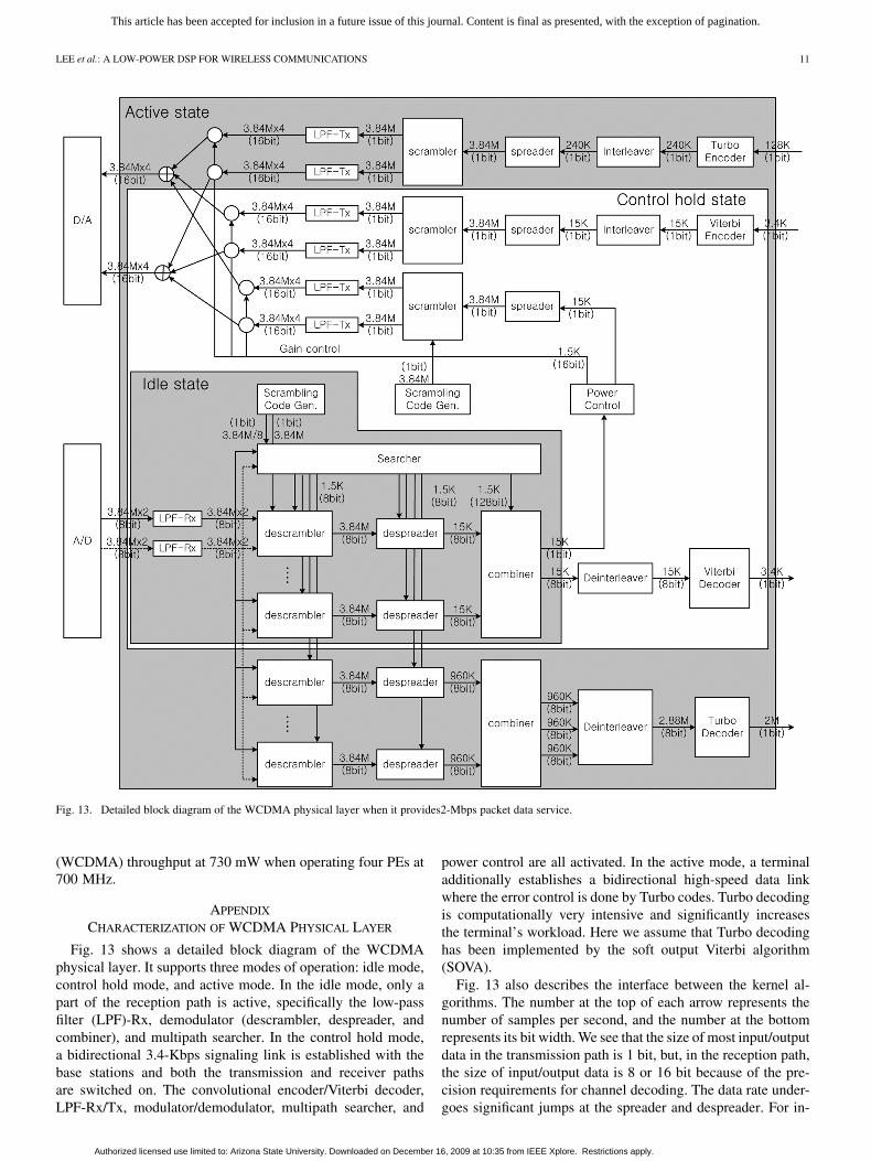
Fig. 13. Detailed block diagram of the WCDMA physical layer when it provides2-Mbps packet data service.
(WCDMA) throughput at 730 mW when operating four PEs at700 MHz.
APPENDIX
CHARACTERIZATION OF WCDMA PHYSICAL LAYER
Fig. 13 shows a detailed block diagram of the WCDMAphysical layer. It supports three modes of operation: idle mode,control hold mode, and active mode. In the idle mode, only apart of the reception path is active, specifically the low-passfilter (LPF)-Rx, demodulator (descrambler, despreader, andcombiner), and multipath searcher. In the control hold mode,a bidirectional 3.4-Kbps signaling link is established with thebase stations and both the transmission and receiver pathsare switched on. The convolutional encoder/Viterbi decoder,LPF-Rx/Tx, modulator/demodulator, multipath searcher, and
power control are all activated. In the active mode, a terminaladditionally establishes a bidirectional high-speed data linkwhere the error control is done by Turbo codes. Turbo decodingis computationally very intensive and significantly increasesthe terminal’s workload. Here we assume that Turbo decodinghas been implemented by the soft output Viterbi algorithm(SOVA).
Fig. 13 also describes the interface between the kernel al-gorithms. The number at the top of each arrow represents thenumber of samples per second, and the number at the bottomrepresents its bit width. We see that the size of most input/outputdata in the transmission path is 1 bit, but, in the reception path,the size of input/output data is 8 or 16 bit because of the pre-cision requirements for channel decoding. The data rate under-goes significant jumps at the spreader and despreader. For in-
Authorized licensed use limited to: Arizona State University. Downloaded on December 16, 2009 at 10:35 from IEEE Xplore. Restrictions apply.
This article has been accepted for inclusion in a future issue of this journal. Content is final as presented, with the exception of pagination.
12 IEEE TRANSACTIONS ON VERY LARGE SCALE INTEGRATION (VLSI) SYSTEMS
TABLE XIPEAK WORKLOAD PROFILE OF THE WCDMA PHYSICAL LAYER FOR THE THREE OPERATION MODES
stance, in the transmission path, the data rate is upconvertedfrom kilosamples per second into megasamples per second afterthe spreading operation.
The detailed peak workload profile of the WCDMA physicallayer is shown in Table XI. This was generated by compiling theW-CDMA benchmark (written in C) with an Alpha gcc com-piler, and executing it on the M5 architecture simulator [19]. Theinstruction count required to finish each algorithm was taken andthe peak workload of each algorithm calculated by dividing theinstruction count by the tightest processing time requirement ofthe algorithm.
The first thing to note in Table XI is that the total workloadvaries significantly with the operation mode. For instance, thetotal workload in the idle mode is only 14% of that in the activemode. Second, kernel algorithms and the workload assigned tothem also vary according to the operation mode. For instance,the multipath searcher has the same workload in the active andcontrol hold modes but significantly lower workload in the idlemode. In general, the workload in the transmission path is muchless than that in the receiver path.
Next we present the parallelism in each of the W-CDMA al-gorithms in Table XII. The second and third columns in the tablepresent the ratio between the run time of the scalar code andthe vector code. The fourth column represents the maximumpossible data-level parallelism, DLP, defined as the maximumSIMD vector width. The fifth column provides the bit width ofthe two vector operands in the fifth column. The last columnshows the thread-level parallelism, TLP.
From Table XII, we can see that the searcher, LPF, scrambler,descrambler, and the BMC/ACS of the Viterbi decoder exhibitconsiderable DLP and TLP. The DLP of the scrambler and de-scrambler can be converted into TLP by subdividing large vec-tors into smaller ones. The Turbo decoder contains limited DLPbecause the allowed maximum vector length of the ACS opera-tion of the Turbo decoder is 8. It is possible to increase the DLPby decoding multiple blocks simultaneously.
Table XII also shows that there are several algorithms thatcannot be parallelized. Examples include the interleaver, dein-terleaver, spreader, despreader, and combiner. However, theworkload of these algorithms is not significant as shown inTable XI. Therefore we can easily increase system throughput
TABLE XIIPARALLELISM AVAILABLE IN THE ALGORITHMS
OF THE WCDMA PHYSICAL LAYER
and power efficiency by exploiting the inherent DLP and TLPshown in Table XII. From this analysis, we conclude that thearchitecture should support both scalar and vector operationsand that the architecture should especially be optimized forvector operations.
REFERENCES
[1] H.-M. Bluethgen, C. Grassmann, W. Raab, and U. Ramacher, “A pro-grammable baseband platform for software-defined radio,” presentedat the SDR Tech. Conf. and Product Exposition, Nov. 2004.
[2] J. Fridman and Z. Greenfield, “The TigerSHARC DSP architecture,”IEEE Micro, vol. 20, no. 1, pp. 66–76, Jan./Feb. 2000.
[3] S. Knowles, “The SOC future is soft,” in IEE Cambridge Branch Sem-inar, Dec. 2005.
[4] K. v. Berkel, F. Heinle, P. Meuwissen, K. Moerman, and M. Weiss,“Vector processing as an enabler for software-defined radio in hand-held devices,” EURASIP J. Appl. Signal Process., vol. 2005, no. 16,pp. 2613–2625, 2005.
[5] J. Glossner, D. Lancu, L. Jin, E. Hokenek, and M. Moudgill, “Asoftware-defined communications baseband design,” IEEE Commun.Mag., vol. 41, no. 1, pp. 120–128, Jan. 2003.
Authorized licensed use limited to: Arizona State University. Downloaded on December 16, 2009 at 10:35 from IEEE Xplore. Restrictions apply.

This article has been accepted for inclusion in a future issue of this journal. Content is final as presented, with the exception of pagination.
LEE et al.: A LOW-POWER DSP FOR WIRELESS COMMUNICATIONS 13
[6] A. Nilsson, E. Tell, and D. Liu, “An 11 mm 70 mW fully-pro-grammable baseband processor for mobile WiMAX and DVB-T/H in0.12 �m CMOS,” in Proc. IEEE Int. Solid-State Circuits Conf., Feb.2008, pp. 266–267.
[7] Y. Lin, H. Lee, M. Woh, Y. Harel, S. Mahlke, T. Mudge, C.Chakrabarti, and K. Flautner, “SODA: A low-power architecture forsoftware radio,” in Proc. Int. Symp. Comput. Architecture, Jun. 2006,pp. 89–101.
[8] A. Duller, G. Panesar, and D. Towner, “Parallel processing—The Pic-oChip way!,” Commun. Process Arch., pp. 125–138, Sep. 2003.
[9] A. Lodi, A. Cappelli, M. Bocchi, C. Mucci, M. Innocenti, C. D. Bar-tolomeis, L. Ciccarelli, R. Giansante, A. Deledda, F. Campi, M. Toma,and R. Guerrieri, “XiSystem: A XiRisc-based SoC with reconfigurableI/O module,” IEEE J. Solid-State Circuits, vol. 41, no. 1, pp. 85–96,Jan. 2006.
[10] A. Chun, E. Tsui, I. Chen, H. Honary, and J. Lin, “Application ofIntel reconfigurable architecture to 802.11a, 3G and 4G standards,” pre-sented at the Circuit and System Symp. Emerging Technologies, Fron-tiers of Mobile and Wireless Communications, May 2004.
[11] QuickSilver Technology [Online]. Available: http://www.qstech.com[12] G. Smit, A. Kokkeler, P. Wolkotte, P. Hölzenspies, M. Burgwal, and
P. Heysters, “The chameleon architecture for streaming DSP applica-tions,” EURASIP J. Embedded Syst., vol. 2007, Art. no. 78082.
[13] B. Mei, S. Vernalde, D. Verkest, and R. Lauwereins, “Design method-ology for a tightly coupled VLIW/reconfigurable matrix architecture:A case study,” in Design Automation and Test in Europe, 2004, vol. 2,pp. 21 224–21 229.
[14] WCDMA for UMTS: Radio Access for Third Generation Mobile Com-munications, H. Holma and A. Toskala, Eds. Hoboken, NJ: Wiley ,2000.
[15] P. Roshan and J. Leary, 802.11 Wireless LAN Fundamentals. Indi-anapolis, IN: Cisco Press, 2003.
[16] D. Talla, L. John, and D. Burger, “Bottlenecks in multimedia pro-cessing with SIMD style extensions and architectural enhancements,”IEEE Trans. Comput., vol. 52, no. 8, pp. 1015–1031, Aug. 2003.
[17] H. Hunter and J. Moreno, “A new look at exploiting data parallelism inembedded systems,” in Proc. Int. Conf. Compilers, Architecture, andSynthesis for Embedded Syst., Oct. 2003, pp. 159–169.
[18] H. Lee, “A baseband processor for software defined radio terminals,”Ph.D. thesis, Univ. Michigan, Ann Arbor, MI, 2007.
[19] N. L. Binkert et al., “The M5 simulator: Modeling networked systems,”IEEE Micro, vol. 26, no. 4, pp. 52–60, Jul./Aug. 2006.
Hyunseok Lee (M’08) received the Ph.D. degree incomputer science and engineering from the Univer-sity of Michigan, Ann Arbor, in 2007.
He is currently an Assistant Professor in theDepartment of Electronics and CommunicationsEngineering, Kwangwoon University, Seoul, Korea.From 1992 to 2008, he participated in the develop-ment of IS-95, cdma2000, WCDMA, and mobileWiMAX systems at Samsung Electronics, Suwon,Korea. His research interest includes low-powersignal processing architectures and embedded sys-
tems for wireless communications.
Chaitali Chakrabarti (S’86–M’89–SM’02) is aProfessor of electrical engineering at Arizona StateUniversity, Tempe. Her research interests includeall aspects of low-power embedded systems designand VLSI architectures and algorithms for signalprocessing, image processing, and communications.
Dr. Chakrabarti served as the Technical Com-mittee Chair of the DISPS subcommittee, IEEESignal Processing Society (2006–2007). She iscurrently an Associate Editor of the Journal ofVLSI Signal Processing Systems and the IEEE
TRANSACTIONS ON VERY LARGE SCALE INTEGRATION SYSTEMS.
Trevor Mudge (S’74–M’77–SM’84–F’95) receivedthe Ph.D. degree in computer science from the Uni-versity of Illinois, Urbana-Champaign.
Since then, he has been at the University ofMichigan, Ann Arbor. He was named the BredtProfessor of Engineering after a ten-year term asDirector of the Advanced Computer ArchitectureLaboratory—a group of a dozen faculty and 80graduate students. He is an author of numerouspapers on computer architecture, programminglanguages, VLSI design, and computer vision. He
has also chaired 40 theses in these areas.Dr. Mudge is a Fellow of the IEEE, a member of the ACM, the IET, and the
British Computer Society.
Authorized licensed use limited to: Arizona State University. Downloaded on December 16, 2009 at 10:35 from IEEE Xplore. Restrictions apply.