Embed Size (px)
Citation preview
IEEE TRANSACTIONS ON POWER ELECTRONICS, VOL. 19, NO. 4, JULY 2004 947
Zero-Voltage-Switching Half-Bridge DC–DCConverter With Modified PWM Control Method
Hong Mao, Jaber Abu-Qahouq, Member, IEEE, Shiguo Luo, and Issa Batarseh, Senior Member, IEEE
Abstract—Asymmetric control scheme is an approach toachieve zero-voltage switching (ZVS) for half-bridge isolateddc–dc converters. However, it is not suited for wide range of inputvoltage due to the uneven voltage and current components stresses.This paper presents a novel “duty-cycle-shifted pulse-width mod-ulated” (DCS PWM) control scheme for half-bridge isolated dc–dcconverters to achieve ZVS operation for one of the two switcheswithout causing the asymmetric penalties in the asymmetriccontrol and without adding additional components. Based on theDCS PWM control scheme, an active-clamp branch comprisingan auxiliary switch and a diode is added across the isolationtransformer primary winding in the half-bridge converter toachieve ZVS for the other main switch by utilizing energy storedin the transformer leakage inductance. Moreover, the auxiliaryswitch also operates at ZVS and zero-current switching (ZCS)conditions. Furthermore, during the off-time period, the ringingresulted from the oscillation between the transformer leakageinductance and the junction capacitance of two switches is elimi-nated owing to the active-clamp branch and DCS PWM controlscheme. Hence, switching losses and leakage-inductance-relatedlosses are significantly reduced, which provides the converter withthe potential to operate at higher efficiencies and higher switchingfrequencies. The principle of operation and key features of theproposed DCS PWM control scheme and two ZVS half-bridgetopologies are illustrated and experimentally verified.
Index Terms—Duty-cycle-shifted (DCS), half bridge (HB),metal oxide semiconductor field effect transistors (MOSFETs),pulse-width modulated (PWM), zero-current switching (ZCS),zero-voltage switching (ZVS).
I. INTRODUCTION
SEVERAL new techniques for high frequency dc–dcconversion have been proposed to reduce component
stresses and switching losses while achieving high powerdensity and improved performance [1]–[11]. Among them,the phase-shifted zero-voltage-switching (ZVS) full bridge[1]–[3] is one of the most attractive techniques since it allowsall switches to operate at ZVS by utilizing transformer leakageinductance and metal oxide semiconductor field effect tran-sistors’ (MOSFETs) junction capacitance without adding an
Manuscript received December 30, 2002; revised August 19, 2003. This workwas recommended for publication by Associate Editor P. K. Jain upon evaluationof the reviewers’ comments.
H. Mao was with the School of Electrical Engineering and Computer Science,University of Central Florida, Orlando, FL 32816 USA and is now with AstecPower, Andover, MA 01810 USA.
J. Abu-Qahouq and I. Batarseh are with the School of Electrical Engineeringand Computer Science, University of Central Florida, Orlando, FL 32816 USA(e-mail: [email protected]).
S. Luo was with the School of Electrical Engineering and Computer Science,University of Central Florida, Orlando, FL 32816 USA. He is now with ArtesynTechnologies, Framingham, MA 01701 USA.
Digital Object Identifier 10.1109/TPEL.2004.830052
auxiliary switch. However, the complexity of the full-bridgeis almost highest among the conventional topologies due toits large switch count and complicated control and driving.Active-clamp forward topology [4]–[6] is another typicalexample to successfully realize ZVS for the switches byutilizing the leakage inductance, magnetizing inductance andjunction capacitance. However, the topology of the converteris asymmetric and the energy-delivery is unidirectional. Inother words, voltage and current stresses are unevenly dis-tributed, which results in the individual switch and rectifierstresses being higher compared to symmetric half-bridge andfull-bridge converters. This disadvantage limits power level ofthe active-clamp forward topology applications. In addition, dcbias of magnetizing current may exist in the transformer [5].
Half bridge (HB) dc–dc converter is an attractive topologyfor middle power level applications owing to its simplicity.There are two conventional control schemes for the HBdc–dc converter, namely, symmetric control and asymmetric(complimentary) control. The main drawback of the con-ventional symmetric control is that both primary switches inthe converter operate at hard switching condition. Moreover,during the off-time period of two switches, the oscillationbetween the transformer leakage inductance and junctioncapacitance of the switches results in energy dissipation andelectromagnetic interference (EMI) emissions due to reverserecovery of MOSFETs body diodes. To suppress the ringing,resistive snubbers are usually added. As a result, energy in thetransformer leakage inductance is significantly dissipated insnubbers. Therefore, the symmetric-control half bridge is not agood candidate for high switching frequency power conversion.
The asymmetric (complementary) control was proposedto achieve ZVS operation for HB switches [7]–[11]. Twodrive signals are complementarily generated and applied tohigh side and low side switches. Thus, the two HB switchesmay be turned on at ZVS conditions owing to the fact thatthe transformer primary current charges and discharges thejunction capacitance. However, asymmetric stresses distri-bution on the corresponding components may occur due tothe asymmetric duty cycle distribution for the two primaryswitches. In other words, current stresses in the two primaryswitches are not identical and voltage and current stresseson secondary rectifiers are not equal. As a result, diodes orsynchronous rectifiers with higher voltage rating are neededat the penalty of degrading the performance and efficiencyof the rectifier stage [10]. Furthermore, the dc gain ratio ofthe converter is nonlinear, thus higher duty cycle variation isneeded for the same input voltage variation in comparison withsymmetric PWM control scheme, which makes the converteroperate further beyond the optimum operating point at high
0885-8993/04$20.00 © 2004 IEEE
Authorized licensed use limited to: ULAKBIM UASL - YILDIZ TEKNIK UNIVERSITESI. Downloaded on August 03,2010 at 12:52:45 UTC from IEEE Xplore. Restrictions apply.
948 IEEE TRANSACTIONS ON POWER ELECTRONICS, VOL. 19, NO. 4, JULY 2004
input voltage [10]. Therefore, the complementary (asymmetric)PWM control is more suitable for applications where the inputvoltage is fixed. As a solution to reduce the duty cycle variationfor wide input voltage range, an asymmetric transformer turnsratio together with integrated-magnetic structure was proposedin [10], such that rectifiers with lower withstanding voltagemay be used to improve the performance. However, the powerdelivery of the transformer and current stresses in the switchesand rectifiers are still uneven [10].
In this paper, a new control scheme, to be known as duty-cycleshifted PWM (DCS PWM) control, is proposed and applied tothe conventional HB dc–dc converters to achieve ZVS for one ofthe two switches without adding extra components and withoutadding asymmetric penalties of the complementary control. Theconcept of this new control scheme is shifting one of the twosymmetric PWM driving signals close to the other, such thatZVS may be achieved for the lagging switch due to the short-ened resonant interval. Unlike the asymmetric control, the widthof the duty cycle for the two switches is kept equal, such thatall corresponding components work at the conditions with evenstresses as the case in the symmetric control scheme.
Moreover, based on the DCS PWM control, a new half-bridgetopology is proposed to achieve ZVS for the other switch andauxiliary switch by adding an auxiliary switch and diode in theconventional half bridge. ZVS for the other switch is achievedby utilizing the energy trapped in the leakage inductance. In ad-dition, the proposed topology with DCS PWM control elim-inates the ringing resulting from the oscillation between thetransformer leakage inductance and the switches junction ca-pacitances during the off-time period. Therefore, the proposedconverter has a potential to operate at higher efficiencies andswitching frequencies. The principle of operation and featuresof the DCS PWM control and proposed topologies are illus-trated and verified experimentally on 36–75 V input voltageprototypes.
Section II describes the DCS PWM control scheme.Section III presents the principle of operation and features ofthe proposed ZVS half-bridge topology with the DCS PWMcontrol scheme. In Section IV, a modified DCS controlledZVS HB topology is presented. Experimental results andcomparisons are presented in Section V and the conclusion isgiven in Section VI.
II. DCS PWM CONTROL SCHEME
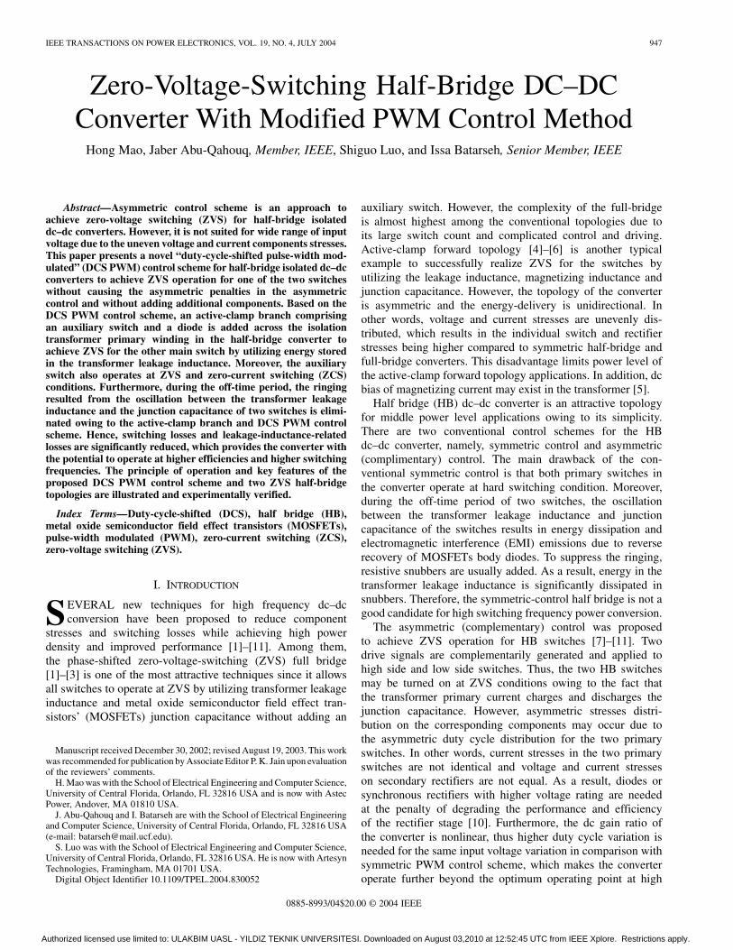
Fig. 1 shows the half-bridge dc–dc converter with currentdoubler rectifier. The ideal waveforms for the symmetric PWMcontrol is sketched in Fig. 2(a), where , is the leakage in-ductance; ip, are the transformer primary-side input andmagnetizing currents, respectively; and is the forward cur-rent through rectifier diode . Besides the hard switching,conventional symmetric PWM control has transformer-leakage-inductance related disadvantages. During the off-time periodwhen both switches are off, the energy stored in the transformerleakage inductance may be recycled to primary dc bus throughbody diodes of MOSFETs. However, because of reverse re-covery current of body diodes, the oscillation between the trans-former leakage inductance and the MOSFETs’ junction capaci-tance is significant on the primary side. To suppress the ringing,usually, snubber circuits are necessarily added, but losses dis-
Fig. 1. Conventional half bridge converter with a current doubler rectifier.
Fig. 2. Waveforms comparison of the half bridge dc–dc converter:(a) symmetric PWM control and (b) DCS PWM control.
sipated in the snubber become dramatically large, especially athigh input current and high switching frequencies.
A. Proposed DCS PWM Control Scheme
Fig. 2(b) shows the key waveforms of the half-bridge con-verter with the proposed DCS PWM control. Based on sym-metric PWM control, driving signal is shifted left suchthat the rising edge is close to the falling edge of drivingsignal . When is turned off, the transformer primarycurrent charges the junction capacitance of switch and dis-charges the junction capacitance of switch . After the voltageacross drain-to-source of drops to zero, the body diode ofconducts to carry the current. During the body diode conduc-tion period, may be turned on at zero-voltage switching. Noringing occurs during the transition period.
Authorized licensed use limited to: ULAKBIM UASL - YILDIZ TEKNIK UNIVERSITESI. Downloaded on August 03,2010 at 12:52:45 UTC from IEEE Xplore. Restrictions apply.
MAO et al.: ZERO-VOLTAGE-SWITCHING HALF-BRIDGE DC–DC CONVERTER 949
Fig. 3. DCS PWM modulation scheme: (a) modulation circuits and (b) keywaveforms.
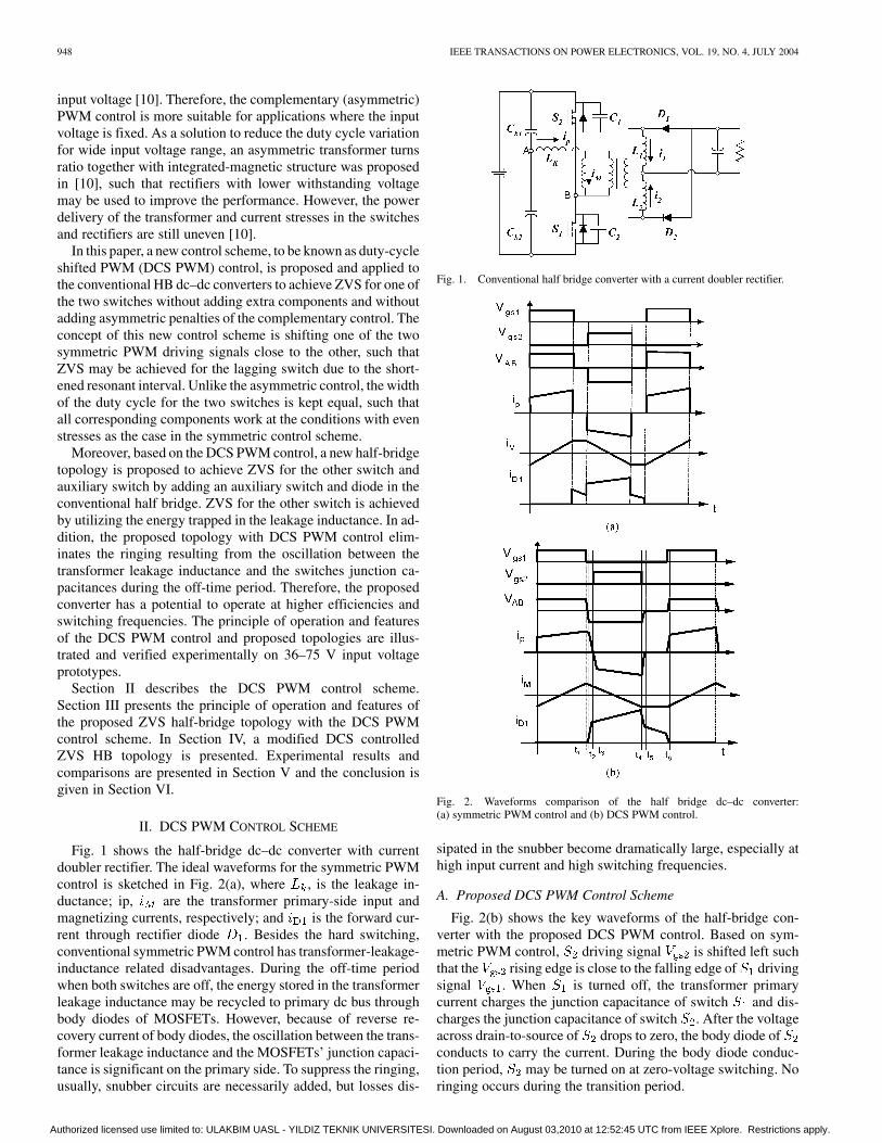
Fig. 3 shows a possible modulation approach for the realiza-tion of DCS PWM control. Where, Vsaw is the SAW carrierwaveform for modulation; and are control voltages de-rived from the front voltage or current controller. By modulating
and , driving signals for and can be generated,respectively. Because the falling time of the saw waveform isshort, the falling edge of is always close to the rising edgeof , which provide a possibility of ZVS for . This mod-ulation method differs from the conventional symmetric PWMmethod in that the direction of variation of the two duty cyclesis opposite as shown in Fig. 3(b) by the arrows shown on thedriving signals waveforms. In other words, since andare symmetrically centered around zero, the duty cycle of isregulated by moving its rising edge left and right, while the dutycycle of is regulated by moving its falling edge right and left,keeping and with the same duty cycle.
B. Principle of Operation
To simplify the analysis of operation, components are con-sidered ideal except otherwise indicated. The main operationmodes are described as follows.
Mode 1 : Initially, is conducting, and the inputpower is delivered to the output. is charged andfreewheels through .Mode 2 : is turned off at ,causing the primary current to charge and discharge
. During the interval, the reflected secondary inductorcurrent dominates the primary current ip. Thus, may bedischarged to zero at wide load range, which means wideZVS range can be achieved for .Mode 3 : When the voltage across is dis-charged to zero at , the body diode of conducts tocarry the current, which provides ZVS condition for switch
. During this period, leakage inductance is reset and sec-ondary current and freewheel through and ,respectively.Mode 4 : is turned on with ZVS at ;the primary current decreases to zero and then becomes
negative. When the negative peak current equals to the re-flected current, the diode is blocked and the con-verter starts to deliver power to the output. The inductoris charged and inductor current continues to freewheel.Mode 5 : is turned off at , causingthe primary current to charge and discharge .When the secondary and start to freewheel, leakageinductance and junction capacitance of switches andstart to oscillate on the primary side. During the interval,body diodes may be involved, which worsens the ringingand results in reverse recovery losses. (The ringing wave-forms are not shown in the Figure.)Mode 6 : The oscillation comes to the endwith equal voltage across switches and . On the sec-ondary side, and keep freewheeling. At ,is turned on again going back to Mode 1.
C. Main Features Compared With Symmetric and AsymmetricPWM Control
Compared with the conventional symmetric PWM control,DCS PWM controlled HB has the same voltage and currentstresses in the primary switches, and although the transformervoltage and current waveforms are different from those of thesymmetric PWM control, the voltage-second value and magne-tizing B-H loop of the transformer are identical. The peak andrms currents through the transformers are also the same for bothschemes. Hence, there is no change in characteristics and designof the transformer from the symmetric PWM control to DCSPWM control.
In the secondary side, as shown in Fig. 2, even though thecurrents through rectifiers have different waveforms in the twoschemes, the peak and rms values of the waveforms are equal.Moreover, the inductors voltage-second value, current peak andcurrent rms values are the same for both schemes. Therefore, thevoltage and current stresses for the secondary-side switches andinductors are the same for both schemes. Consequently, thereis no change in the components selection and converter designwith the change of control scheme from symmetric PWM con-trol to the proposed DCS PWM control.
As mentioned above, both symmetric PWM and DCS PWMhave even voltage and current stresses in corresponding compo-nents thanks to the identical duty cycle width for two switches.Hence, there are no asymmetric penalties in asymmetric PWMcontrol, which allows DCS PWM control to be employed inapplications for wide input voltage range. Furthermore, in theDCS PWM control, ZVS for switch is achieved withoutadding additional components. In addition, wide ZVS range op-eration may be achieved because the secondary inductor cur-rent is reflected to transformer primary side to the discharge theoutput capacitor of switch to create ZVS condition for switch
. Because switching losses and transformer leakage-induc-tance-related losses are reduced, higher efficiency is expectedwith the DCS PWM control method.
A comparison between the asymmetric HB, symmetric HBand DCS HB under same design conditions is shown in Table I,where is the transformer turn ratio, is the duty cycle ofthe switch , is the load current, is the input voltage,and is the output voltage. The filter inductance and outputcapacitance values are assumed large enough such that the
Authorized licensed use limited to: ULAKBIM UASL - YILDIZ TEKNIK UNIVERSITESI. Downloaded on August 03,2010 at 12:52:45 UTC from IEEE Xplore. Restrictions apply.
950 IEEE TRANSACTIONS ON POWER ELECTRONICS, VOL. 19, NO. 4, JULY 2004
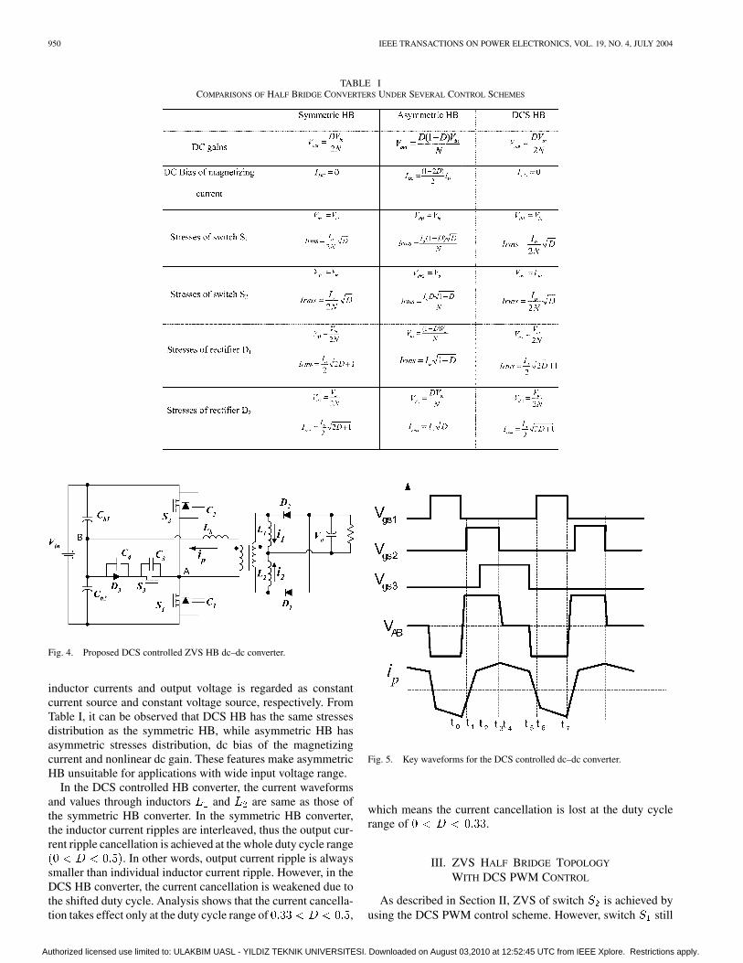
TABLE ICOMPARISONS OF HALF BRIDGE CONVERTERS UNDER SEVERAL CONTROL SCHEMES
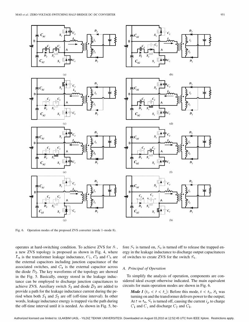
Fig. 4. Proposed DCS controlled ZVS HB dc–dc converter.
inductor currents and output voltage is regarded as constantcurrent source and constant voltage source, respectively. FromTable I, it can be observed that DCS HB has the same stressesdistribution as the symmetric HB, while asymmetric HB hasasymmetric stresses distribution, dc bias of the magnetizingcurrent and nonlinear dc gain. These features make asymmetricHB unsuitable for applications with wide input voltage range.
In the DCS controlled HB converter, the current waveformsand values through inductors and are same as those ofthe symmetric HB converter. In the symmetric HB converter,the inductor current ripples are interleaved, thus the output cur-rent ripple cancellation is achieved at the whole duty cycle range
. In other words, output current ripple is alwayssmaller than individual inductor current ripple. However, in theDCS HB converter, the current cancellation is weakened due tothe shifted duty cycle. Analysis shows that the current cancella-tion takes effect only at the duty cycle range of ,
Fig. 5. Key waveforms for the DCS controlled dc–dc converter.
which means the current cancellation is lost at the duty cyclerange of .
III. ZVS HALF BRIDGE TOPOLOGY
WITH DCS PWM CONTROL
As described in Section II, ZVS of switch is achieved byusing the DCS PWM control scheme. However, switch still
Authorized licensed use limited to: ULAKBIM UASL - YILDIZ TEKNIK UNIVERSITESI. Downloaded on August 03,2010 at 12:52:45 UTC from IEEE Xplore. Restrictions apply.
MAO et al.: ZERO-VOLTAGE-SWITCHING HALF-BRIDGE DC–DC CONVERTER 951
Fig. 6. Operation modes of the proposed ZVS converter (mode 1–mode 8).
operates at hard-switching condition. To achieve ZVS for ,a new ZVS topology is proposed as shown in Fig. 4, where
is the transformer leakage inductance, , and arethe external capacitors including junction capacitance of theassociated switches, and is the external capacitor acrossthe diode . The key waveforms of the topology are showedin the Fig. 5. Basically, energy stored in the leakage induc-tance can be employed to discharge junction capacitances toachieve ZVS. Auxiliary switch and diode are added toprovide a path for the leakage inductance current during the pe-riod when both and are off (off-time interval). In otherwords, leakage inductance energy is trapped via the path duringthe off-time interval until it is needed. As shown in Fig. 5, be-
fore is turned on, is turned off to release the trapped en-ergy in the leakage inductance to discharge output capacitancesof switches to create ZVS for the switch .
A. Principal of Operation
To simplify the analysis of operation, components are con-sidered ideal except otherwise indicated. The main equivalentcircuits for main operation modes are shown in Fig. 6.
Mode 1 : Before this mode, , wasturning on and the transformer delivers power to the output;At , is turned off, causing the current to charge
and and discharge and .
Authorized licensed use limited to: ULAKBIM UASL - YILDIZ TEKNIK UNIVERSITESI. Downloaded on August 03,2010 at 12:52:45 UTC from IEEE Xplore. Restrictions apply.
952 IEEE TRANSACTIONS ON POWER ELECTRONICS, VOL. 19, NO. 4, JULY 2004
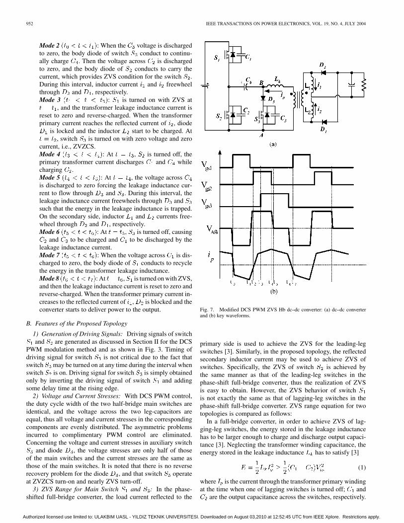
Mode 2 : When the voltage is dischargedto zero, the body diode of switch conduct to continu-ally charge . Then the voltage across is dischargedto zero, and the body diode of conducts to carry thecurrent, which provides ZVS condition for the switch .During this interval, inductor current and freewheelthrough and , respectively.Mode 3 : is turned on with ZVS at
, and the transformer leakage inductance current isreset to zero and reverse-charged. When the transformerprimary current reaches the reflected current of , diode
is locked and the inductor start to be charged. At, switch is turned on with zero voltage and zero
current, i.e., ZVZCS.Mode 4 : At , is turned off, theprimary transformer current discharges and whilecharging .Mode 5 : At , the voltage acrossis discharged to zero forcing the leakage inductance cur-rent to flow through and . During this interval, theleakage inductance current freewheels through andsuch that the energy in the leakage inductance is trapped.On the secondary side, inductor and currents free-wheel through and , respectively.Mode 6 : At , is turned off, causing
and to be charged and to be discharged by theleakage inductance current.Mode 7 : When the voltage across is dis-charged to zero, the body diode of conducts to recyclethe energy in the transformer leakage inductance.Mode 8 : At , is turned on with ZVS,and then the leakage inductance current is reset to zero andreverse-charged. When the transformer primary current in-creases to the reflected current of , is blocked and theconverter starts to deliver power to the output.
B. Features of the Proposed Topology
1) Generation of Driving Signals: Driving signals of switchand are generated as discussed in Section II for the DCS
PWM modulation method and as shown in Fig. 3. Timing ofdriving signal for switch is not critical due to the fact thatswitch may be turned on at any time during the interval whenswitch is on. Driving signal for switch is simply obtainedonly by inverting the driving signal of switch and addingsome delay time at the rising edge.
2) Voltage and Current Stresses: With DCS PWM control,the duty cycle width of the two half-bridge main switches areidentical, and the voltage across the two leg-capacitors areequal, thus all voltage and current stresses in the correspondingcomponents are evenly distributed. The asymmetric problemsincurred to complimentary PWM control are eliminated.Concerning the voltage and current stresses in auxiliary switch
and diode , the voltage stresses are only half of thoseof the main switches and the current stresses are the same asthose of the main switches. It is noted that there is no reverserecovery problem for the diode , and that switch operateat ZVZCS turn-on and nearly ZVS turn-off.
3) ZVS Range for Main Switch and : In the phase-shifted full-bridge converter, the load current reflected to the
Fig. 7. Modified DCS PWM ZVS Hb dc–dc converter: (a) dc–dc converterand (b) key waveforms.
primary side is used to achieve the ZVS for the leading-legswitches [3]. Similarly, in the proposed topology, the reflectedsecondary inductor current may be used to achieve ZVS ofswitches. Specifically, the ZVS of switch is achieved bythe same manner as that of the leading-leg switches in thephase-shift full-bridge converter, thus the realization of ZVSis easy to obtain. However, the ZVS behavior of switchis not exactly the same as that of lagging-leg switches in thephase-shift full-bridge converter. ZVS range equation for twotopologies is compared as follows:
In a full-bridge converter, in order to achieve ZVS of lag-ging-leg switches, the energy stored in the leakage inductancehas to be larger enough to charge and discharge output capaci-tance [3]. Neglecting the transformer winding capacitance, theenergy stored in the leakage inductance has to satisfy [3]
(1)
where is the current through the transformer primary windingat the time when one of lagging switches is turned off; and
are the output capacitance across the switches, respectively.
Authorized licensed use limited to: ULAKBIM UASL - YILDIZ TEKNIK UNIVERSITESI. Downloaded on August 03,2010 at 12:52:45 UTC from IEEE Xplore. Restrictions apply.
MAO et al.: ZERO-VOLTAGE-SWITCHING HALF-BRIDGE DC–DC CONVERTER 953
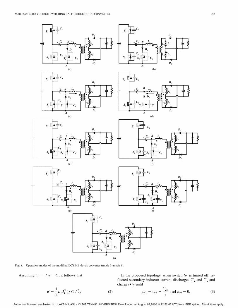
Fig. 8. Operation modes of the modified DCS HB dc–dc converter (mode 1–mode 9).
Assuming , it follows that
(2)
In the proposed topology, when switch is turned off, re-flected secondary inductor current discharges and andcharges until
(3)
Authorized licensed use limited to: ULAKBIM UASL - YILDIZ TEKNIK UNIVERSITESI. Downloaded on August 03,2010 at 12:52:45 UTC from IEEE Xplore. Restrictions apply.
954 IEEE TRANSACTIONS ON POWER ELECTRONICS, VOL. 19, NO. 4, JULY 2004
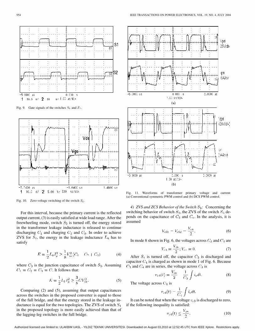
Fig. 9. Gate signals of the switches S and S .
Fig. 10. Zero-voltage switching of the switch S .
For this interval, because the primary current is the reflectedoutput current, (3) is easily satisfied at wide load range. After thefreewheeling mode, switch is turned off, the energy storedin the transformer leakage inductance is released to continuedischarging and charging and . In order to achieveZVS for , the energy in the leakage inductance has tosatisfy
(4)
where is the junction capacitance of switch . Assuming. It follows that:
(5)
Comparing (2) and (5), assuming that output capacitancesacross the switches in the proposed converter is equal to thoseof the full bridge, and that the energy stored in the leakage in-ductance is equal for the two topologies. The ZVS of switchin the proposed topology is more easily achieved than that ofthe lagging-leg switches in the full bridge.
Fig. 11. Waveforms of transformer primary voltage and current:(a) Conventional symmetric PWM control and (b) DCS PWM control.
4) ZVS and ZCS Behavior of the Switch : Concerning theswitching behavior of switch , the ZVS of the switch de-pends on the capacitance of and . In the analysis, it isassumed
(6)
In mode 8 shown in Fig. 6, the voltages across and are
(7)
After is turned off, the capacitor is discharged andcapacitor is charged as shown in mode 1 of Fig. 6. Because
and are in series, the voltage across is
(8)
The voltage across is
(9)
It can be noted that when the voltage is discharged to zero,if the following inequality is satisfied:
(10)
Authorized licensed use limited to: ULAKBIM UASL - YILDIZ TEKNIK UNIVERSITESI. Downloaded on August 03,2010 at 12:52:45 UTC from IEEE Xplore. Restrictions apply.
MAO et al.: ZERO-VOLTAGE-SWITCHING HALF-BRIDGE DC–DC CONVERTER 955
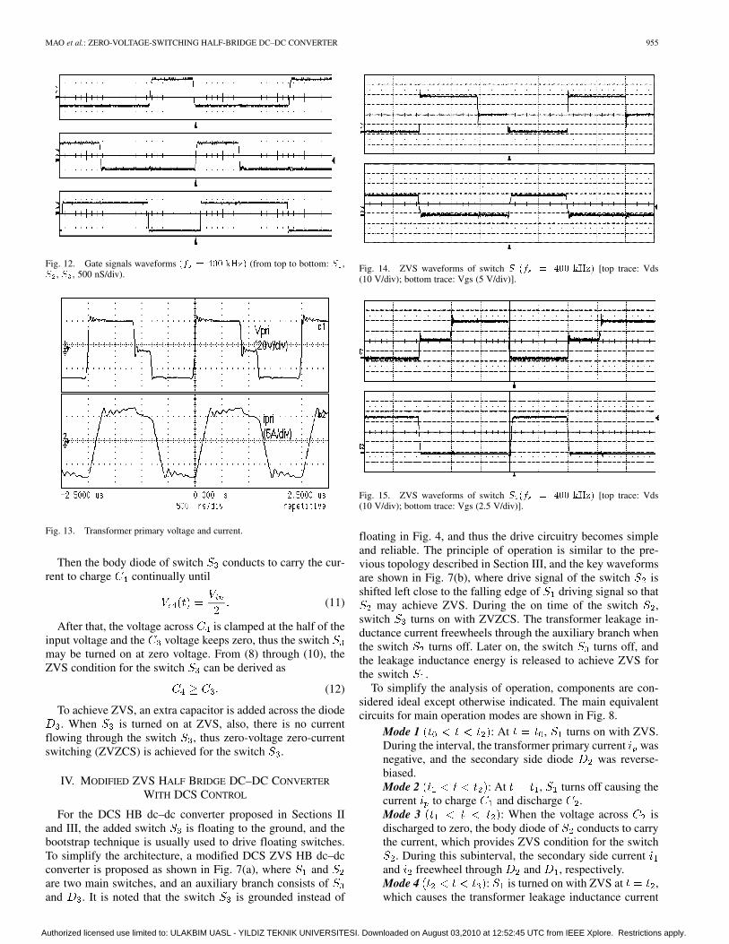
Fig. 12. Gate signals waveforms (f = 400 kHz) (from top to bottom: S ,S , S , 500 nS/div).
Fig. 13. Transformer primary voltage and current.
Then the body diode of switch conducts to carry the cur-rent to charge continually until
(11)
After that, the voltage across is clamped at the half of theinput voltage and the voltage keeps zero, thus the switchmay be turned on at zero voltage. From (8) through (10), theZVS condition for the switch can be derived as
(12)
To achieve ZVS, an extra capacitor is added across the diode. When is turned on at ZVS, also, there is no current
flowing through the switch , thus zero-voltage zero-currentswitching (ZVZCS) is achieved for the switch .
IV. MODIFIED ZVS HALF BRIDGE DC–DC CONVERTER
WITH DCS CONTROL
For the DCS HB dc–dc converter proposed in Sections IIand III, the added switch is floating to the ground, and thebootstrap technique is usually used to drive floating switches.To simplify the architecture, a modified DCS ZVS HB dc–dcconverter is proposed as shown in Fig. 7(a), where andare two main switches, and an auxiliary branch consists ofand . It is noted that the switch is grounded instead of
Fig. 14. ZVS waveforms of switch S (f = 400 kHz) [top trace: Vds(10 V/div); bottom trace: Vgs (5 V/div)].
Fig. 15. ZVS waveforms of switch S (f = 400 kHz) [top trace: Vds(10 V/div); bottom trace: Vgs (2.5 V/div)].
floating in Fig. 4, and thus the drive circuitry becomes simpleand reliable. The principle of operation is similar to the pre-vious topology described in Section III, and the key waveformsare shown in Fig. 7(b), where drive signal of the switch isshifted left close to the falling edge of driving signal so that
may achieve ZVS. During the on time of the switch ,switch turns on with ZVZCS. The transformer leakage in-ductance current freewheels through the auxiliary branch whenthe switch turns off. Later on, the switch turns off, andthe leakage inductance energy is released to achieve ZVS forthe switch .
To simplify the analysis of operation, components are con-sidered ideal except otherwise indicated. The main equivalentcircuits for main operation modes are shown in Fig. 8.
Mode 1 : At , turns on with ZVS.During the interval, the transformer primary current wasnegative, and the secondary side diode was reverse-biased.Mode 2 : At , turns off causing thecurrent to charge and discharge .Mode 3 : When the voltage across isdischarged to zero, the body diode of conducts to carrythe current, which provides ZVS condition for the switch
. During this subinterval, the secondary side currentand freewheel through and , respectively.Mode 4 : is turned on with ZVS at ,which causes the transformer leakage inductance current
Authorized licensed use limited to: ULAKBIM UASL - YILDIZ TEKNIK UNIVERSITESI. Downloaded on August 03,2010 at 12:52:45 UTC from IEEE Xplore. Restrictions apply.
956 IEEE TRANSACTIONS ON POWER ELECTRONICS, VOL. 19, NO. 4, JULY 2004
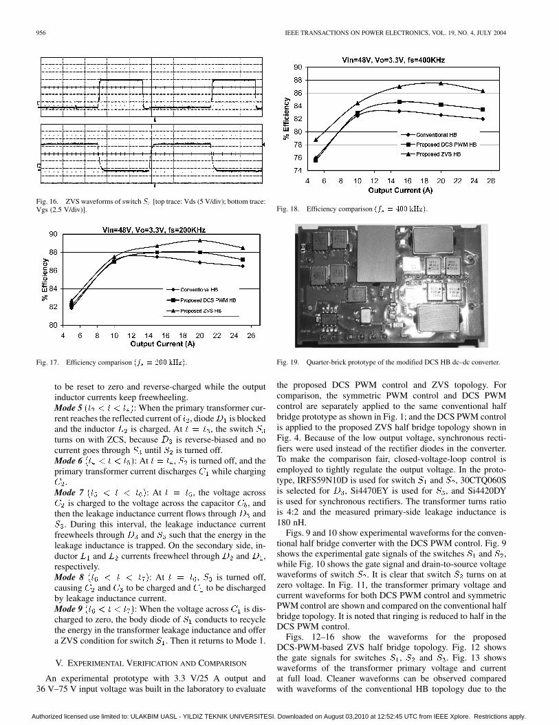
Fig. 16. ZVS waveforms of switch S [top trace: Vds (5 V/div); bottom trace:Vgs (2.5 V/div)].
Fig. 17. Efficiency comparison (f = 200 kHz).
to be reset to zero and reverse-charged while the outputinductor currents keep freewheeling.Mode 5 : When the primary transformer cur-rent reaches the reflected current of , diode is blockedand the inductor is charged. At , the switchturns on with ZCS, because is reverse-biased and nocurrent goes through until is turned off.Mode 6 : At , is turned off, and theprimary transformer current discharges while charging
.Mode 7 : At , the voltage across
is charged to the voltage across the capacitor , andthen the leakage inductance current flows through and
. During this interval, the leakage inductance currentfreewheels through and such that the energy in theleakage inductance is trapped. On the secondary side, in-ductor and currents freewheel through and ,respectively.Mode 8 : At , is turned off,causing and to be charged and to be dischargedby leakage inductance current.Mode 9 : When the voltage across is dis-charged to zero, the body diode of conducts to recyclethe energy in the transformer leakage inductance and offera ZVS condition for switch . Then it returns to Mode 1.
V. EXPERIMENTAL VERIFICATION AND COMPARISON
An experimental prototype with 3.3 V/25 A output and36 V–75 V input voltage was built in the laboratory to evaluate
Fig. 18. Efficiency comparison (f = 400 kHz).
Fig. 19. Quarter-brick prototype of the modified DCS HB dc–dc converter.
the proposed DCS PWM control and ZVS topology. Forcomparison, the symmetric PWM control and DCS PWMcontrol are separately applied to the same conventional halfbridge prototype as shown in Fig. 1; and the DCS PWM controlis applied to the proposed ZVS half bridge topology shown inFig. 4. Because of the low output voltage, synchronous recti-fiers were used instead of the rectifier diodes in the converter.To make the comparison fair, closed-voltage-loop control isemployed to tightly regulate the output voltage. In the proto-type, IRFS59N10D is used for switch and , 30CTQ060Sis selected for , Si4470EY is used for , and Si4420DYis used for synchronous rectifiers. The transformer turns ratiois 4:2 and the measured primary-side leakage inductance is180 nH.
Figs. 9 and 10 show experimental waveforms for the conven-tional half bridge converter with the DCS PWM control. Fig. 9shows the experimental gate signals of the switches and ,while Fig. 10 shows the gate signal and drain-to-source voltagewaveforms of switch . It is clear that switch turns on atzero voltage. In Fig. 11, the transformer primary voltage andcurrent waveforms for both DCS PWM control and symmetricPWM control are shown and compared on the conventional halfbridge topology. It is noted that ringing is reduced to half in theDCS PWM control.
Figs. 12–16 show the waveforms for the proposedDCS-PWM-based ZVS half bridge topology. Fig. 12 showsthe gate signals for switches , and . Fig. 13 showswaveforms of the transformer primary voltage and currentat full load. Cleaner waveforms can be observed comparedwith waveforms of the conventional HB topology due to the
Authorized licensed use limited to: ULAKBIM UASL - YILDIZ TEKNIK UNIVERSITESI. Downloaded on August 03,2010 at 12:52:45 UTC from IEEE Xplore. Restrictions apply.
MAO et al.: ZERO-VOLTAGE-SWITCHING HALF-BRIDGE DC–DC CONVERTER 957
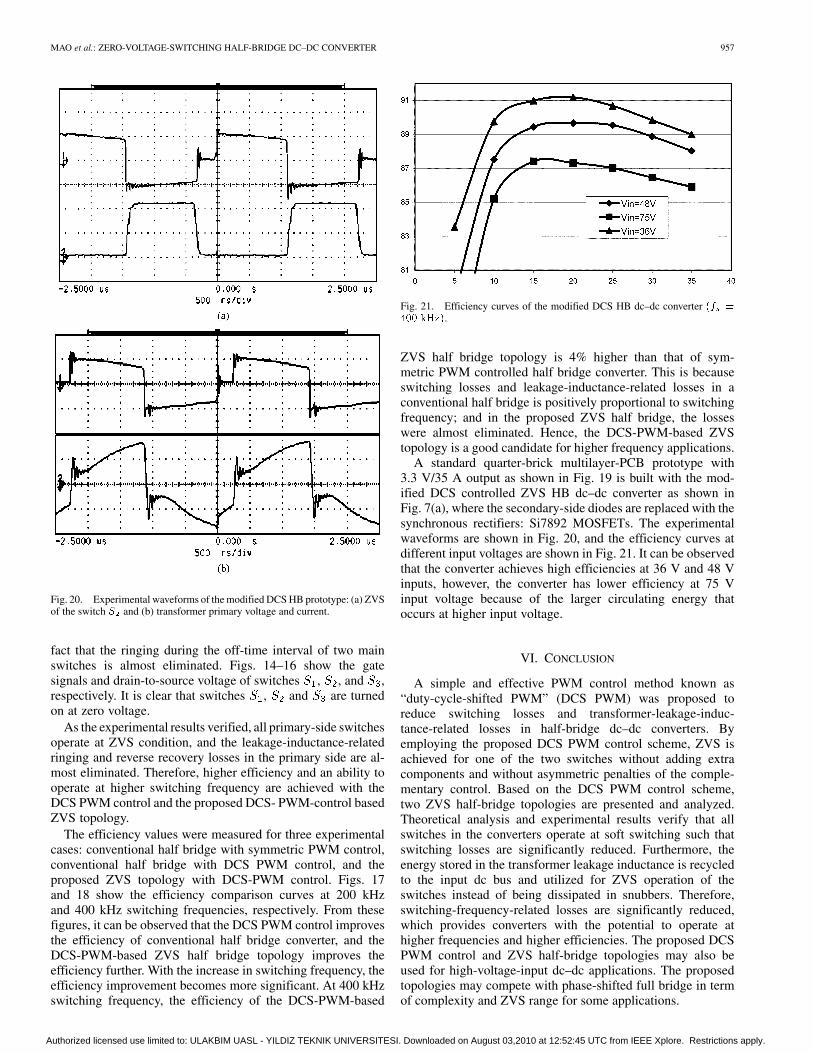
Fig. 20. Experimental waveforms of the modified DCS HB prototype: (a) ZVSof the switch S and (b) transformer primary voltage and current.
fact that the ringing during the off-time interval of two mainswitches is almost eliminated. Figs. 14–16 show the gatesignals and drain-to-source voltage of switches , , and ,respectively. It is clear that switches , and are turnedon at zero voltage.
As the experimental results verified, all primary-side switchesoperate at ZVS condition, and the leakage-inductance-relatedringing and reverse recovery losses in the primary side are al-most eliminated. Therefore, higher efficiency and an ability tooperate at higher switching frequency are achieved with theDCS PWM control and the proposed DCS- PWM-control basedZVS topology.
The efficiency values were measured for three experimentalcases: conventional half bridge with symmetric PWM control,conventional half bridge with DCS PWM control, and theproposed ZVS topology with DCS-PWM control. Figs. 17and 18 show the efficiency comparison curves at 200 kHzand 400 kHz switching frequencies, respectively. From thesefigures, it can be observed that the DCS PWM control improvesthe efficiency of conventional half bridge converter, and theDCS-PWM-based ZVS half bridge topology improves theefficiency further. With the increase in switching frequency, theefficiency improvement becomes more significant. At 400 kHzswitching frequency, the efficiency of the DCS-PWM-based
Fig. 21. Efficiency curves of the modified DCS HB dc–dc converter (f =400 kHz).
ZVS half bridge topology is 4% higher than that of sym-metric PWM controlled half bridge converter. This is becauseswitching losses and leakage-inductance-related losses in aconventional half bridge is positively proportional to switchingfrequency; and in the proposed ZVS half bridge, the losseswere almost eliminated. Hence, the DCS-PWM-based ZVStopology is a good candidate for higher frequency applications.
A standard quarter-brick multilayer-PCB prototype with3.3 V/35 A output as shown in Fig. 19 is built with the mod-ified DCS controlled ZVS HB dc–dc converter as shown inFig. 7(a), where the secondary-side diodes are replaced with thesynchronous rectifiers: Si7892 MOSFETs. The experimentalwaveforms are shown in Fig. 20, and the efficiency curves atdifferent input voltages are shown in Fig. 21. It can be observedthat the converter achieves high efficiencies at 36 V and 48 Vinputs, however, the converter has lower efficiency at 75 Vinput voltage because of the larger circulating energy thatoccurs at higher input voltage.
VI. CONCLUSION
A simple and effective PWM control method known as“duty-cycle-shifted PWM” (DCS PWM) was proposed toreduce switching losses and transformer-leakage-induc-tance-related losses in half-bridge dc–dc converters. Byemploying the proposed DCS PWM control scheme, ZVS isachieved for one of the two switches without adding extracomponents and without asymmetric penalties of the comple-mentary control. Based on the DCS PWM control scheme,two ZVS half-bridge topologies are presented and analyzed.Theoretical analysis and experimental results verify that allswitches in the converters operate at soft switching such thatswitching losses are significantly reduced. Furthermore, theenergy stored in the transformer leakage inductance is recycledto the input dc bus and utilized for ZVS operation of theswitches instead of being dissipated in snubbers. Therefore,switching-frequency-related losses are significantly reduced,which provides converters with the potential to operate athigher frequencies and higher efficiencies. The proposed DCSPWM control and ZVS half-bridge topologies may also beused for high-voltage-input dc–dc applications. The proposedtopologies may compete with phase-shifted full bridge in termof complexity and ZVS range for some applications.
Authorized licensed use limited to: ULAKBIM UASL - YILDIZ TEKNIK UNIVERSITESI. Downloaded on August 03,2010 at 12:52:45 UTC from IEEE Xplore. Restrictions apply.
958 IEEE TRANSACTIONS ON POWER ELECTRONICS, VOL. 19, NO. 4, JULY 2004
ACKNOWLEDGMENT
The authors would like to thank G. Potter, dc–dc AdvancedTechnology, ASTEC Power, for his support and thoughtful in-sight and advice, B. Higgins, ASTEC Power, for his technicalsupport and helpful discussion, and S. Deng, University of Cen-tral Florida, for his experimental support.
REFERENCES
[1] W. Chen, F. C. Lee, M. M. Jovanovic, and J. A. Sabate, “A comparativestudy of class of full bridge zero-voltage-switched PWM converters,” inProc. IEEE Applied Power Electronics Conf., 1995, pp. 893–899.
[2] R. Redl, N. O. Sokal, and L. Balogh, “A novel soft-switching full-bridgeconverter: Analysis, design considerations, and experimental results at1.5 kW, 100 kHz,” in IEEE Power Electronics Specialists Conf. Records,1990, pp. 162–172.
[3] J. A. Sabate, V. Vlatkovuc, R. B. Ridley, F. C. Lee, and B. I. Cho,“Design considerations for high-voltage high-power full-bridge zero-voltage-switching PWM converter,” in Proc. Applied Power ElectronicsConf. and Exposition (APEC’90), 1990, pp. 275–284.
[4] G. A. Karvelis, M. D. Manolarou, P. Malatestas, and S. N. Manias,“Analysis and design of nondissipative active clamp for forward con-verters,” Proc. Inst. Elect. Eng., vol. 148, no. 5, pp. 419–424, Sept. 2001.
[5] Q. Li, F. C. Lee, and M. M. Jovanovi, “Design considerations of trans-former dc bias of forward converter with active-clamp reset,” in Proc.Applied Power Electronics Conf. and Exposition (APEC’99), 1999, pp.553–559.
[6] H. K. Ji and H. J. Kim, “Active clamp forward converter with MOSFETsynchronous rectification,” in Proc. IEEE Power Electronics SpecialistsConf., 1994, pp. 895–901.
[7] O. Garcia, J. A. Cobos, J. Uceda, and J. Sebastian, “Zero voltageswitching in the PWM half bridge topology with complementarycontrol and synchronous rectification,” in Proc. Power ElectronicsSpecialists Conf. (PESC’95), 1995, pp. 286–291.
[8] J. Sebastian, J. A. Cobos, O. Garcia, and J. Uceda, “An overall studyof the half-bridge complementary-control dc-to-dc converter,” in Proc.Power Electronics Specialists Conf., 1995, pp. 1229–1235.
[9] R. Miftakhutdinov, A. Nemchinov, V. Meleshin, and S. Fraidlin, “Mod-ified asymmetrical ZVS half-bridge dc–dc converter,” in Proc. AppliedPower Electronics Conf. and Exposition (APEC’99), 1999, pp. 567–574.
[10] W. Chen, P. Xu, and F. C. Lee, “The optimization of asymmetric halfbridge converter,” in Proc. Applied Power Electronics Conf., 2001, pp.703–707.
[11] P. Imbertson and N. Mohan, “Asymmetrical duty cycle permits zeroswitching loss in PWM circuits with no conduction loss penalty,” IEEETrans. Power Electron., vol. 29, pp. 121–125, Jan. 1993.
Hong Mao received the B.S. degree from SichuanUniversity of Science and Technology, China, in1992, the M.S. degree from Chongqing University,China, in 1997, and the Ph.D. degree from Zhe-jiang University, China, in 2000, all in electricalengineering.
He is now with Astec Power, Andover, MA From1992 to 1994, he was an Assistant Professor with theDepartment of Electrical Engineering, Sichuan Uni-versity of Science and Technology, where he taughtelectronic courses and did research on motion con-
trol. From 1999 to 2000, he was a Project Leader in the ZTE (Zhongxing)Telecom Corporation, Shenzhen, China, where he developed three phase PWMrectifiers for Uninterrupted Power Systems. From 2000 to 2001, he was a SeniorEngineer and Division Manager with PI Electronics, Hong Kong, China, and heled a team to develop adaptors for SONY laptop computers. From 2001 to 2002,he was with the Center for Power Electronics Systems, Virginia Polytechnic In-stitute and State University (Virginia Tech), Blacksburg, focusing on high-effi-ciency front-end dc–dc converters. In February 2002, he joined the University ofCentral Florida, Orlando, working on low-profile low-voltage dc–dc converters,where he was a Research Scientist and Assistant Director of the Florida PowerElectronics Center, University of Central Florida.
Jaber Abu-Qahouq (M’01) received the B.Sc. de-gree (with first class honors) from Princess SumayaUniversity/Royal Scientific Society, Amman, Jordan,in 1998 and the M.S. and Ph.D. degrees from the Uni-versity of Central Florida, Orlando, in 2000 and 2003,respectively, all in electrical engineering/electronics.
He is currently a Visiting Assistant Professor withthe School of Electrical Engineering and ComputerScience, University of Central Florida. He haspublished more than 20 research papers and severalpatents. He worked on several projects funded by
the Florida Space Consortium, NASA, the National Science Foundation, AstecPower, Intel, and the University of Central Florida. His research interestsinclude soft-switching power conversion, low-profile high-density low-voltagehigh-current fast-transient dc–dc converters, power factor correction converters,digital control in power electronics, and dc–ac inverters.
Dr. Abu-Qahouq is a member of several professional societies and has re-ceived several awards.
Shiguo Luo received the B.S. degree in industrialautomation from the Southwest Institute of Tech-nology, Sichuan, China, in 1985, the Ph.D. degree inelectrical engineering from Chongqing University,Chongqing, China, in 1993, and the Ph.D. degree inelectrical engineering from the University of CentralFlorida (UCF), Orlando, in 2001.
In 1985, he was an Assistant Lecturer and lateran Associate Professor with the Department of Auto-matic Engineering, Chongqing Engineering Institute,Chongqing, China. From 1993 to 1995, he was with
the School of Electrical Engineering, Southwest Jiaotong University, Sichuan,China, as a Post-Doctoral Fellow. From 1997 to 1998, he was a Visiting Pro-fessor in the Virginia Power Electronics Center (now CPES), Virginia Poly-technic Institute and State University, Blacksburg. On January 1, 1999, he joinedthe Power Electronics Research Group, UCF, as a Senior Research Associateand later a Ph.D. Candidate. In more than 15 years of professional experience,he has also worked for Huawei Technology Ltd., Shenzhen, China and LucentTechnologies (Tyco) Power Systems, Inc., Mesquite, TX. He is now a SeniorDesign Engineer at Artesyn Technologies, Framingham, MA. His current re-search interests are product-oriented analysis and design techniques of powerconverters and power electronic systems.
Issa Batarseh (S’84–M’85–SM’92) received theB.S. degree in computer engineering and the M.S.and Ph.D. degrees in electrical engineering all fromthe University of Illinois, Chicago, in 1983, 1985,and 1990, respectively.
He is a Professor and Interim Chair in the Elec-trical and Computer Engineering Department, Uni-versity of Central Florida (UCF), Orlando. He was aVisiting Assistant Professor of Electrical Engineeringat Purdue University, West Lafayette, IN, from 1989to 1990, before joining the Department of Electrical
and Computer Engineering at UCF in 1991. His major research interest is powerelectronics, focusing on high frequency dc–dc conversion, soft-switching anddynamic modeling of dc-to-dc converters, harmonic analysis, and power factorcorrection. He has more than 14 U.S. patents, and more than 50 refereed journaland 200 conference publications. His research work has been sponsored by Fed-eral agencies and the private sector. He has published Power Electronic Circuits(New York: Wiley, 2003).
Dr. Batarseh received many national and international teaching, research, andservice awards. He is a member of Eta Kappa Nu. He has served as SessionChairs and Committee Member for APEC and PESC conferences. He will bethe General Chair for the PESC’07 Conference, Orlando, FL. He has served asa Chairman of the IEEE Orlando Power Engineering Chapter, Chairman of theIEEE Orlando Section, and as Faculty Advisor for the IEEE Student Branch.He is a Registered Professional Engineer in Florida.
Authorized licensed use limited to: ULAKBIM UASL - YILDIZ TEKNIK UNIVERSITESI. Downloaded on August 03,2010 at 12:52:45 UTC from IEEE Xplore. Restrictions apply.