Embed Size (px)
Citation preview
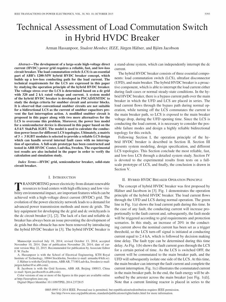
IEEE TRANSACTIONS ON POWER ELECTRONICS, VOL. 30, NO. 10, OCTOBER 2015 5393
Technical Assessment of Load Commutation Switchin Hybrid HVDC Breaker
Arman Hassanpoor, Student Member, IEEE, Jurgen Hafner, and Bjorn Jacobson
Abstract—The development of a large-scale high-voltage directcurrent (HVDC) power grid requires a reliable, fast, and low-losscircuit breaker. The load commutation switch (LCS) is an essentialpart of ABB’s 1200-MW hybrid HVDC breaker concept, whichbuilds up a low-loss conducting path for the load current. Thetechnical requirements for the LCS are expressed in this paperby studying the operation principle of the hybrid HVDC breaker.The voltage stress over the LCS is determined based on a dc gridwith 320 and 2 kA rated voltage and current. A system modelof the hybrid HVDC breaker is developed in PSCAD/EMTDC tostudy the design criteria for snubber circuit and arrester blocks.It is observed that conventional snubber circuits are not suitablefor a bidirectional LCS as the current of snubber capacitors pre-vent the fast interruption action. A modified snubber circuit isproposed in this paper along with two more alternatives for theLCS to overcome this problem. Moreover, the power loss modelfor a semiconductor device is discussed in this paper based on the4.5-kV StakPak IGBT. The model is used to calculate the conduc-tion power losses for different LCS topologies. Ultimately, a matrixof 3 × 3 IGBT modules is selected to provide a reliable LCS designwhich can handle several internal fault cases with no interrup-tion of operation. A full-scale prototype has been constructed andtested in ABB HVDC Center, Ludvika, Sweden. The experimentaltest results are also included in the paper in order to verify thecalculation and simulation study.
Index Terms—HVDC grid, semiconductor breaker, solid-statecircuit breaker.
I. INTRODUCTION
TRANSPORTING power electricity from distant renewableresources to load centers with high efficiency and low visi-
bility environmental impact, are important features which can beachieved with a high-voltage direct current (HVDC) grid. Theevolution of the power electricity network leads to a demand foradvanced power transmission methods and more dc grids. Thekey equipment for developing the dc grid and dc switchyards isthe dc circuit breaker [1], [2]. The lack of a fast and reliable dcbreaker has always been an issue preventing the development ofdc grids but this obstacle has now been removed by introducingthe hybrid HVDC breaker in [3]. The hybrid HVDC breaker is
Manuscript received July 18, 2014; revised October 13, 2014; acceptedNovember 10, 2014. Date of publication November 20, 2014; date of cur-rent version May 22, 2015. Recommended for publication by Associate EditorF. W. Fuchs
A. Hassanpoor is with the School of Electrical Engineering, KTH RoyalInstitute of Technology, 10044 Stockholm, Sweden (e-mail: [email protected]).
J. Hafner is with the Grid Systems, ABB AB, 77180 Ludvika, Sweden (e-mail:[email protected]).
B. Jacobson is with the Grid Systems, ABB AB, Beijing 100015, China(e-mail: [email protected]).
Color versions of one or more of the figures in this paper are available onlineat http://ieeexplore.ieee.org.
Digital Object Identifier 10.1109/TPEL.2014.2372815
a stand-alone system, which can independently interrupt the dccurrent.
The hybrid HVDC breaker consists of three essential compo-nents: load commutation switch (LCS), ultrafast disconnector(UFD), and main breaker. The hybrid HVDC breaker is a proac-tive component, which is able to interrupt the load current eitherduring fault cases or normal steady-state conditions. In the hy-brid HVDC breaker, there is a bypass current path over the mainbreaker in which the UFD and LCS are placed in series. Theload current flows through the bypass path during normal op-eration, while turning off the LCS commutates the current tothe main breaker path, so LCS is exposed to the main breakervoltage drop, during the UFD opening time. Since the LCS isconducting the load current, it is necessary to consider the pos-sible failure modes and design a highly reliable bidirectionaltopology for this switch.
Following Section I, the operation principle of the hy-brid HVDC breaker is described in Section II. Section IIIpresents system modeling, design specification, and differentLCS topologies. This Section conclude the most reliable, fast,and low-loss LCS through a detailed system study. Section IVis devoted to the experimental results from tests on a full-scale prototype of LCS, and finally, the conclusion is drawn inSection V.
II. HYBRID HVDC BREAKER OPERATION PRINCIPLE
The concept of hybrid HVDC breaker was first proposed byHafner and Jacobson in [3]. Fig. 1 demonstrates the operationprinciple of the hybrid HVDC breaker. The load current flowsthrough the UFD and LCS during normal operation. The greenline in Fig. 1(a) shows the load current path during this time. Inthe case of any fault, the conducting current will increase pro-portionally to the fault current and, subsequently, the fault modewill be triggered according to grid requirements and protectionscenarios. In this study, an increase of 20% in the conduct-ing current above the nominal current has been set as a triggerthreshold, so the LCS turn-off signal is initiated at conductingcurrent equal to 2.4 kA, which is followed by decision makingtime delay. The fault type can be determined during this timedelay. As Fig. 1(b) shows the fault current goes through the LCSfor a certain period of time. As the LCS is switched OFF, thecurrent will be commutated to the main breaker path, and theUFD will subsequently isolate one side of the LCS. At this time,the main breaker can interrupt the fault current and complete thecurrent interruption. Fig. 1(c) illustrates the commutated currentin the main breaker path. In the end, the fault energy will be ab-sorbed by the arrester across the main breaker [see Fig. 1(d)].Note that a current limiting reactor is placed in series to the
0885-8993 © 2014 IEEE. Personal use is permitted, but republication/redistribution requires IEEE permission.See http://www.ieee.org/publications standards/publications/rights/index.html for more information.
5394 IEEE TRANSACTIONS ON POWER ELECTRONICS, VOL. 30, NO. 10, OCTOBER 2015
Fig. 1. Hybrid HVDC breaker operation principle. (a) Normal load currentpath. (b) Fault initiates operation. (c) LCS interrupts and commutates currentto main breaker. (d) Main breaker interrupts and commutates current to thearrester.
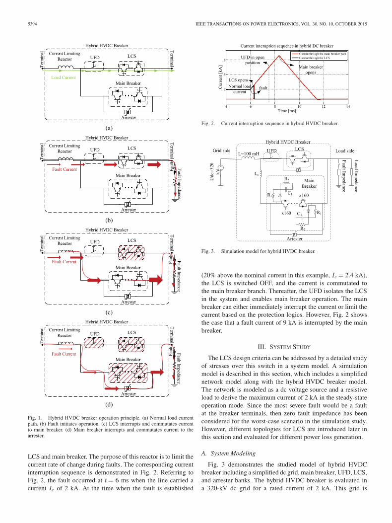
LCS and main breaker. The purpose of this reactor is to limit thecurrent rate of change during faults. The corresponding currentinterruption sequence is demonstrated in Fig. 2. Referring toFig. 2, the fault occurred at t = 6 ms when the line carried acurrent Ic of 2 kA. At the time when the fault is established
Fig. 2. Current interruption sequence in hybrid HVDC breaker.
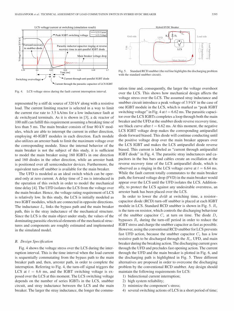
Fig. 3. Simulation model for hybrid HVDC breaker.
(20% above the nominal current in this example, Ic = 2.4 kA),the LCS is switched OFF, and the current is commutated tothe main breaker branch. Thereafter, the UFD isolates the LCSin the system and enables main breaker operation. The mainbreaker can either immediately interrupt the current or limit thecurrent based on the protection logics. However, Fig. 2 showsthe case that a fault current of 9 kA is interrupted by the mainbreaker.
III. SYSTEM STUDY
The LCS design criteria can be addressed by a detailed studyof stresses over this switch in a system model. A simulationmodel is described in this section, which includes a simplifiednetwork model along with the hybrid HVDC breaker model.The network is modeled as a dc voltage source and a resistiveload to derive the maximum current of 2 kA in the steady-stateoperation mode. Since the most severe fault would be a faultat the breaker terminals, then zero fault impedance has beenconsidered for the worst-case scenario in the simulation study.However, different topologies for LCS are introduced later inthis section and evaluated for different power loss generation.
A. System Modeling
Fig. 3 demonstrates the studied model of hybrid HVDCbreaker including a simplified dc grid, main breaker, UFD, LCS,and arrester banks. The hybrid HVDC breaker is evaluated ina 320-kV dc grid for a rated current of 2 kA. This grid is
HASSANPOOR et al.: TECHNICAL ASSESSMENT OF LOAD COMMUTATION SWITCH IN HYBRID HVDC BREAKER 5395
Fig. 4. LCS voltage stress during the fault current interruption interval.
represented by a stiff dc source of 320 kV along with a resistiveload. The current limiting reactor is selected in a way to limitthe current rise rate to 3.5 kA/ms for a low inductance fault atdc switchyard terminals. As it is shown in [3], a dc reactor of100 mH can fulfill this requirement assuming a breaking time ofless than 5 ms. The main breaker consists of four 80-kV mod-ules, which are able to interrupt the current in either direction,employing 40-IGBT modules in each direction. Each modulealso utilizes an arrester bank to limit the maximum voltage overthe corresponding module. Since the internal behavior of themain breaker is not the subject of this study, it is sufficientto model the main breaker using 160 IGBTs in one directionand 160 diodes in the other direction, while an arrester bankis positioned over all semiconductor devices. Furthermore, theequivalent turn-off snubber is available for the main breaker.
The UFD is modeled as an ideal switch which can be oper-ated only at zero current. A delay time of 2 ms is introduced inthe operation of this switch in order to model the mechanicaltime delay [4]. The UFD isolates the LCS from the voltage overthe main breaker. Hence, the voltage rating requirement of LCSis relatively low. In this study, the LCS is initially modeled astwo IGBT modules, which are connected in opposite directions.The inductance Ls links the bypass path and the main breakerpath, this is the stray inductance of the mechanical structure.Since the LCS is the main object under study, the values of thedominating parasitic electrical elements of the mechanical struc-tures and components are roughly estimated and implementedin the simulated model.
B. Design Specification
Fig. 4 shows the voltage stress over the LCS during the inter-ruption interval. This is the time interval when the load currentis sequentially commutating from the bypass path to the mainbreaker path and, then, arrester path, in order to complete theinterruption. Referring to Fig. 4, the turn-off signal triggers theLCS at t = 6.6 ms, and the IGBT switching voltage is ex-posed over the LCS at this moment. The LCS switching voltagedepends on the number of series IGBTs in the LCS, snubbercircuit, and stray inductance between the LCS and the mainbreaker. The larger the stray inductance, the longer the commu-
Fig. 5. Standard RCD snubber (the red line highlights the discharging problemwith the standard snubber circuit).
tation time and, consequently, the larger the voltage overshootover the LCS. This shows how mechanical design affects thevoltage stress over the LCS. The assumed stray inductance andsnubber circuit introduce a peak voltage of 3.9 kV in the case ofone IGBT module in the LCS, which is marked as “peak IGBTswitching voltage” in Fig. 4 at t = 6.62 ms. The parasitic capaci-tor over the LCS IGBTs completes a loop through both the mainbreaker and the UFD at the snubber diode reverse recovery time,see black curve after t = 6.62 ms. At this moment, the negativeLCS IGBT voltage drop makes the corresponding antiparalleldiode forward biased. This diode will continue conducting untilthe positive voltage drop over the main breaker appears overthe LCS IGBT and makes the LCS antiparallel diode reversebiased. This current is labeled as “current through antiparallelIGBT diode” in Fig. 4. The parasitic stray inductances and ca-pacitors in the bus bars and cables create an oscillation at thereverse recovery time of the LCS antiparallel diode, which isobserved as a ringing in the LCS voltage curve at t = 6.64 ms.While the fault current totally commutates to the main breakerpath, the forward voltage drop (FVD) in the main breaker wouldappear over the LCS until the UFD isolates the LCS. Addition-ally, to protect the LCS against any undesirable overstress, anarrester bank has been placed over the LCS.
In order to lower the dv/dt at switching time, a resistor–capacitor diode (RCD) turn-off snubber is placed at each IGBTmodule in LCS. Standard RCD snubber is shown in Fig. 5. Rs
is the turn-on resistor, which controls the discharging behaviourof the snubber capacitor Cs at turn on time. The diode Ds
bypasses Rs during the turn-off period in order to reduce theIGBT stress and charge the snubber capacitor as fast as possible.However, using the conventional RCD snubber for LCS preventsfast UFD action, because the snubber capacitor Cs has a lowresistive path to be discharged through the Rs , UFD, and mainbreaker during the breaking action. The discharging current goesthrough the UFD and precludes fast opening action. The currentthrough the UFD and the main breaker is plotted in Fig. 6, andthe discharging path is highlighted in Fig. 5. Three differentalternatives are proposed in order to overcome the dischargingproblem by the conventional RCD snubber. Any design shouldmaintain the following requirements for LCS:
1) bidirectional current interruption;2) high system reliability;3) minimize the component’s stress;4) several switching actions of LCS in a short period of time;

5396 IEEE TRANSACTIONS ON POWER ELECTRONICS, VOL. 30, NO. 10, OCTOBER 2015
Fig. 6. Current through the main breaker path and bypass path.
5) simple mechanical structure;6) low-conduction loss.1) Alternative One (Reversal Connection): Using a diode in
series with the LCS will prevent the snubber capacitor to bedischarged through the main breaker. In this case, the standardRCD snubber can be used, while the same configuration shouldbe used as an antiparallel connected LCS to enable bidirectionaloperation of the hybrid HVDC breaker. However, a resistor isused in parallel to the snubber capacitor to discharge the capac-itor with a large time constant. This facilitates a more securemaintenance period and lowers risk to personnel. Fig. 7(a) illus-trates the topology for this alternative. Another advantage of thistopology is that only one IGBT stack will conduct the currentin each direction so the conduction losses only include IGBTlosses and no diode loss in the antiparallel IGBT diodes. Thediode power loss is only generated through the series diodes D1and D2 in this alternative.
2) Alternative Two (Modified Snubber Circuit): A modifiedsnubber circuit is presented in Fig. 7(b). During the turn-offperiod, C1 is charged and shapes the switching voltage overthe corresponding IGBT. While the current commutation is ac-complished, the stored charge in C1 will be shared by parallelcapacitor C2 through R2 . Thereafter, C1 can handle anotherswitching action in the corresponding IGBT. The capacitanceof C2 needs to be at least three times higher than C1 and R2resistance also needs to be much smaller than R1 . Moreover, R1ensures capacitor discharge with a relatively large time constant.A typical value for this snubber circuit is as follows:
1) C1 = 7.5 μF, C2 = 20 μF;2) R1 = 10 kΩ, R2 = 10 Ω;3) Alternative Three (Snubber IGBT): In order to unify the
mechanical design along with the full functionality of the turn-off snubber, an IGBT module can be placed in the snubber cir-cuit according to Fig. 7(c). All LCS IGBTs, including snubberIGBTs, are switched simultaneously; therefore, no additionalfiring pulse control logic needs to be implemented for the snub-ber IGBT. The snubber IGBT will block the discharging cur-rent through the snubber resistance at turn-off, while it formsa discharging path through the snubber resistance at the timethat LCS IGBT is switched on again. This feature allows fastturn-on turn-off actions for LCS with no excessive over voltageformation over the IGBT modules [5].
C. LCS Topology
Regardless which of the above mentioned snubber configu-rations is used, the LCS continuously conducts the load current
(a)
(b)
(c)
Fig. 7. (a) Alternative one (series diode connection). (b) Alternative two(modified snubber circuit). (c) Alternative three (snubber IGBT).
in steady-state operation. In this section, a reliable and robustdesign of the LCS is addressed by providing an additional con-ducting path and also decreasing the stresses on each internalcomponent.
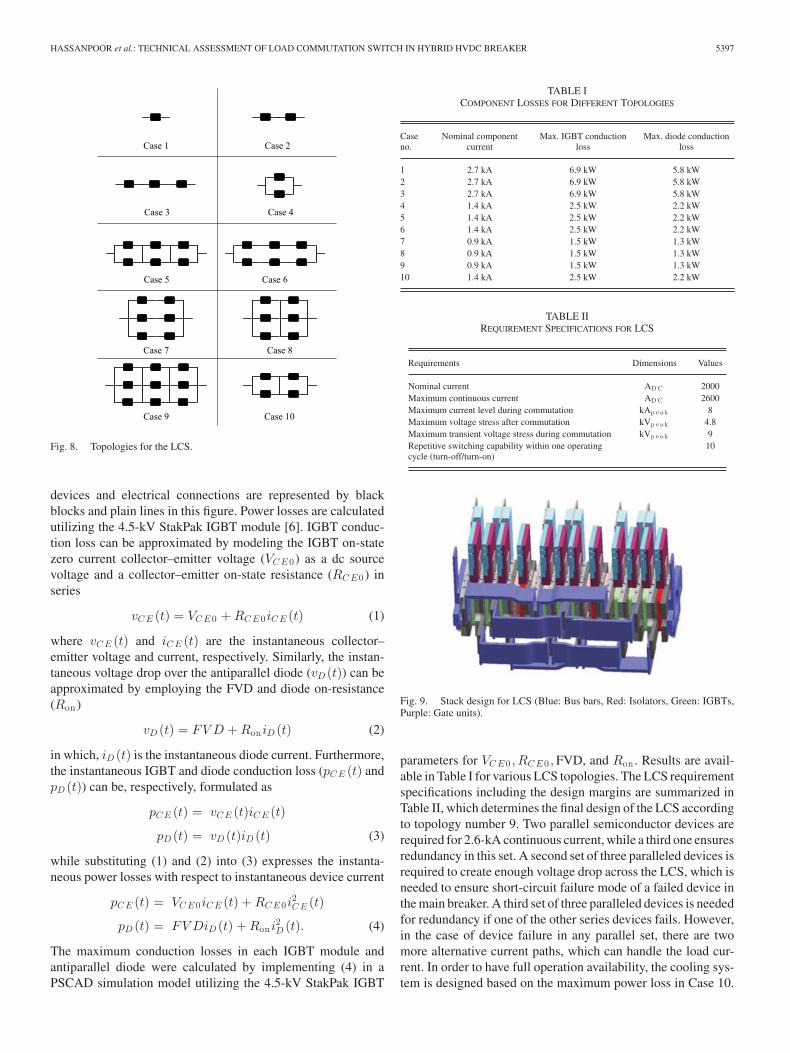
Additional conducting paths can be provided by parallelingthe semiconductor devices in the LCS, while series connectionresults in a lower voltage stress on each device. Therefore, theLCS reliability can be improved through paralleling and seriesconnection of semiconductor devices. On the other hand, eachsemiconductor device contributes to power losses and also in-crease the total system complexity, so an optimized design forthe LCS is a tradeoff between system reliability, power loss, andsystem complexity. However, ten different LCS topologies havebeen studied and evaluated regarding the component stresses andlosses. These cases are depicted in Fig. 8. The semiconductor
HASSANPOOR et al.: TECHNICAL ASSESSMENT OF LOAD COMMUTATION SWITCH IN HYBRID HVDC BREAKER 5397
Fig. 8. Topologies for the LCS.
devices and electrical connections are represented by blackblocks and plain lines in this figure. Power losses are calculatedutilizing the 4.5-kV StakPak IGBT module [6]. IGBT conduc-tion loss can be approximated by modeling the IGBT on-statezero current collector–emitter voltage (VC E 0) as a dc sourcevoltage and a collector–emitter on-state resistance (RC E 0) inseries
vC E (t) = VC E 0 + RC E 0iC E (t) (1)
where vC E (t) and iC E (t) are the instantaneous collector–emitter voltage and current, respectively. Similarly, the instan-taneous voltage drop over the antiparallel diode (vD (t)) can beapproximated by employing the FVD and diode on-resistance(Ron )
vD (t) = FV D + RoniD (t) (2)
in which, iD (t) is the instantaneous diode current. Furthermore,the instantaneous IGBT and diode conduction loss (pC E (t) andpD (t)) can be, respectively, formulated as
pC E (t) = vC E (t)iC E (t)
pD (t) = vD (t)iD (t) (3)
while substituting (1) and (2) into (3) expresses the instanta-neous power losses with respect to instantaneous device current
pC E (t) = VC E 0iC E (t) + RC E 0i2C E (t)
pD (t) = FV DiD (t) + Roni2D (t). (4)
The maximum conduction losses in each IGBT module andantiparallel diode were calculated by implementing (4) in aPSCAD simulation model utilizing the 4.5-kV StakPak IGBT
TABLE ICOMPONENT LOSSES FOR DIFFERENT TOPOLOGIES
Caseno.
Nominal componentcurrent
Max. IGBT conductionloss
Max. diode conductionloss
1 2.7 kA 6.9 kW 5.8 kW2 2.7 kA 6.9 kW 5.8 kW3 2.7 kA 6.9 kW 5.8 kW4 1.4 kA 2.5 kW 2.2 kW5 1.4 kA 2.5 kW 2.2 kW6 1.4 kA 2.5 kW 2.2 kW7 0.9 kA 1.5 kW 1.3 kW8 0.9 kA 1.5 kW 1.3 kW9 0.9 kA 1.5 kW 1.3 kW10 1.4 kA 2.5 kW 2.2 kW
TABLE IIREQUIREMENT SPECIFICATIONS FOR LCS
Requirements Dimensions Values
Nominal current AD C 2000Maximum continuous current AD C 2600Maximum current level during commutation kAp e a k 8Maximum voltage stress after commutation kVp e a k 4.8Maximum transient voltage stress during commutation kVp e a k 9Repetitive switching capability within one operatingcycle (turn-off/turn-on)
10
Fig. 9. Stack design for LCS (Blue: Bus bars, Red: Isolators, Green: IGBTs,Purple: Gate units).
parameters for VC E 0 , RC E 0 , FVD, and Ron . Results are avail-able in Table I for various LCS topologies. The LCS requirementspecifications including the design margins are summarized inTable II, which determines the final design of the LCS accordingto topology number 9. Two parallel semiconductor devices arerequired for 2.6-kA continuous current, while a third one ensuresredundancy in this set. A second set of three paralleled devices isrequired to create enough voltage drop across the LCS, which isneeded to ensure short-circuit failure mode of a failed device inthe main breaker. A third set of three paralleled devices is neededfor redundancy if one of the other series devices fails. However,in the case of device failure in any parallel set, there are twomore alternative current paths, which can handle the load cur-rent. In order to have full operation availability, the cooling sys-tem is designed based on the maximum power loss in Case 10.

5398 IEEE TRANSACTIONS ON POWER ELECTRONICS, VOL. 30, NO. 10, OCTOBER 2015
Fig. 10. Hybrid HVDC breaker test circuit.
In this case, all back-up devices in the LCS are fully used. Inaddition to all above mentioned redundancies in the LCS, an ar-rester block will protect the LCS against any kind of unexpectedstresses, which might occur in internal or external failure cases.This arrester block limits the maximum overvoltage stress to4.5 kV in the case of 4.5-kV StakPak IGBT module utiliza-tion. The final stack design of the LCS is illustrated in Fig. 9.The stack design brings full modularity and easy maintenance.Parallel connections are accomplished through flexible bus barsbetween each set of three series devices, while insulator platesseparate the series sets.
Overall, the LCS is designed in a way that can handle differentfault cases not only inside the LCS, but also in the main breakerpath. Refereing to Table I, the LCS can withstand the maximumload current of 8 kA in the case of any commutation failureoccur in the system. This maxmimum current level correspondsto the 9 kV of transient peak voltage.
IV. EXPERIMENTAL TEST RESULTS
An LCS full-scale prototype has been built according to thedesign specification in Section III-C and the third alternative(snubber IGBT). The designed LCS has been studied in a testcircuit including the main breaker, UFD, and arresters in orderto illustrate the stresses over the LCS components. The testsequence is similar to the introduced functional logic of thehybrid HVDC breaker in Section II. However, the fault currentin this test setup is generated by discharging the capacitor banksand its rate of change (di/dt) is regulated by reactors in the loop.
A. Test Setup
Fig. 10 illustrates the hybrid HVDC breaker test circuit. Thecapacitor bank C1 builds up the desired dc voltage level of
40 kV, supplied by a ±150-kV outdoor dc switchyard. Initially,the breaker Q11 charges the capacitor bank C1. Later, the dcswitchyard will be isolated by opening the breaker Q11. There-after, the capacitor bank C1 discharges through the reactor L1and test object, when the spark gap Q5 triggers the test. The vari-able reactor L1 can be manipulated to achieve different rates ofrise of the current di/dt. The object under test including mainbreaker, UFD, LCS, and arrester bank is represented by Q41,Q42, Q43, and F1, respectively, in Fig. 10. The optical cur-rent measurement devices are also integrated in the test circuitto measure different quantities during the test procedure. T1measures the total discharging current, T2 measures the currentthrough LCS, and T3 measures the arrester current. The break-ers Q21, Q22, Q25, and Q26 are protective breakers ensuringcircuit grounding for safety purposes.
B. Test Results
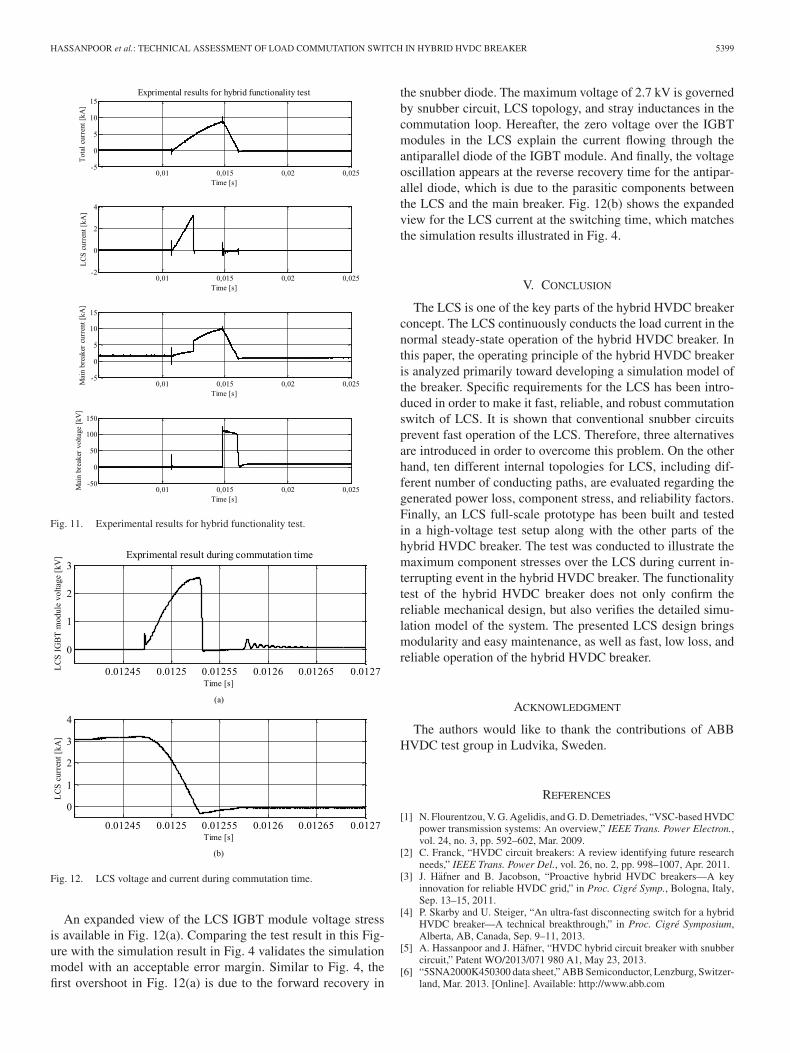
The results from tests are illustrated in Fig. 11. The spark gapQ5 initiates the test at t0 = 0.0112 s. In this test, the discharg-ing current is shared between LCS and the main breaker pathaccording to resistance. Note that only one main breaker stack(80-kV module) is used in this test, otherwise there would notbe any current flow through the main breaker path in normaloperation of the hybrid HVDC breaker. However, the LCS isturned off when the conducting current reaches 3.2 kA. At thismoment, the current commutates to the main breaker path, andas is shown in Fig. 11, the LCS current becomes zero. A de-lay time of 250 μs is assumed for commutation time; therefore,the UFD can be opened after this time delay. Finally, the totalcurrent of 9 kA is interrupted by turning off the main breaker.Fig. 11 shows currents in different paths of the hybrid HVDCbreaker and also voltage stress over the main breaker during thetest interval.
HASSANPOOR et al.: TECHNICAL ASSESSMENT OF LOAD COMMUTATION SWITCH IN HYBRID HVDC BREAKER 5399
Fig. 11. Experimental results for hybrid functionality test.
Fig. 12. LCS voltage and current during commutation time.
An expanded view of the LCS IGBT module voltage stressis available in Fig. 12(a). Comparing the test result in this Fig-ure with the simulation result in Fig. 4 validates the simulationmodel with an acceptable error margin. Similar to Fig. 4, thefirst overshoot in Fig. 12(a) is due to the forward recovery in
the snubber diode. The maximum voltage of 2.7 kV is governedby snubber circuit, LCS topology, and stray inductances in thecommutation loop. Hereafter, the zero voltage over the IGBTmodules in the LCS explain the current flowing through theantiparallel diode of the IGBT module. And finally, the voltageoscillation appears at the reverse recovery time for the antipar-allel diode, which is due to the parasitic components betweenthe LCS and the main breaker. Fig. 12(b) shows the expandedview for the LCS current at the switching time, which matchesthe simulation results illustrated in Fig. 4.
V. CONCLUSION
The LCS is one of the key parts of the hybrid HVDC breakerconcept. The LCS continuously conducts the load current in thenormal steady-state operation of the hybrid HVDC breaker. Inthis paper, the operating principle of the hybrid HVDC breakeris analyzed primarily toward developing a simulation model ofthe breaker. Specific requirements for the LCS has been intro-duced in order to make it fast, reliable, and robust commutationswitch of LCS. It is shown that conventional snubber circuitsprevent fast operation of the LCS. Therefore, three alternativesare introduced in order to overcome this problem. On the otherhand, ten different internal topologies for LCS, including dif-ferent number of conducting paths, are evaluated regarding thegenerated power loss, component stress, and reliability factors.Finally, an LCS full-scale prototype has been built and testedin a high-voltage test setup along with the other parts of thehybrid HVDC breaker. The test was conducted to illustrate themaximum component stresses over the LCS during current in-terrupting event in the hybrid HVDC breaker. The functionalitytest of the hybrid HVDC breaker does not only confirm thereliable mechanical design, but also verifies the detailed simu-lation model of the system. The presented LCS design bringsmodularity and easy maintenance, as well as fast, low loss, andreliable operation of the hybrid HVDC breaker.
ACKNOWLEDGMENT
The authors would like to thank the contributions of ABBHVDC test group in Ludvika, Sweden.
REFERENCES
[1] N. Flourentzou, V. G. Agelidis, and G. D. Demetriades, “VSC-based HVDCpower transmission systems: An overview,” IEEE Trans. Power Electron.,vol. 24, no. 3, pp. 592–602, Mar. 2009.
[2] C. Franck, “HVDC circuit breakers: A review identifying future researchneeds,” IEEE Trans. Power Del., vol. 26, no. 2, pp. 998–1007, Apr. 2011.
[3] J. Hafner and B. Jacobson, “Proactive hybrid HVDC breakers—A keyinnovation for reliable HVDC grid,” in Proc. Cigre Symp., Bologna, Italy,Sep. 13–15, 2011.
[4] P. Skarby and U. Steiger, “An ultra-fast disconnecting switch for a hybridHVDC breaker—A technical breakthrough,” in Proc. Cigre Symposium,Alberta, AB, Canada, Sep. 9–11, 2013.
[5] A. Hassanpoor and J. Hafner, “HVDC hybrid circuit breaker with snubbercircuit,” Patent WO/2013/071 980 A1, May 23, 2013.
[6] “5SNA2000K450300 data sheet,” ABB Semiconductor, Lenzburg, Switzer-land, Mar. 2013. [Online]. Available: http://www.abb.com

5400 IEEE TRANSACTIONS ON POWER ELECTRONICS, VOL. 30, NO. 10, OCTOBER 2015
Arman Hassanpoor (S’13) received the B.Sc. de-gree in electrical power engineering from Shiraz Uni-versity, Shiraz, Iran, in 2005, and the M.Sc. degreein electrical power engineering from the Universityof Chalmers, Gothenburg, Sweden, in 2011. He iscurrently working toward the Ph.D. degree at theDepartment of Electrical Energy Conversion, KTHRoyal Institute of Technology, Stockholm, Sweden.
He is also working as an R&D Engineer withABB Power Systems. His research interest in-cludes high power multilevel converters for HVDC
applications.
Jurgen Hafner received the Dr. Ing. degree in elec-trical engineering from the Technical University ofBerlin, Berlin, Germany, in 1998.
In 1996, he joined ABB Switchgear, Ludvika,Sweden, to work on the development of high-voltageapparatus for HVDC and FACTS applications. Since2000, he has been with ABB Power Systems, Lud-vika. In 2009, he was assigned as an R&D ProjectManager for the development of dc grid breakers andcurrently working for voltage source converter sys-tems. He holds several patents in the areas of optical
instrument transformers, converter valves, and dc breakers. Since 2013, hehas been the Head of the development group responsible for large-scale R&Dprojects in the area of HVDC.
Bjorn Jacobson received the M.Sc. degree in engi-neering physics from Uppsala Universitet, Uppsala,Sweden.
He has been working in different positions in engi-neering, management, and R&D within ABB, since1988, in the areas of high-voltage bushings, convertervalves for HVDC and SVC, HVDC plant mechanicaldesign, and HVDC system development. He has beenthe Project Manager for development of two genera-tions of HVDC Light. He has held the position of theVice-President and the Manager of R&D at ABB’s
global lead center for HVDC, Ludvika, Sweden. He holds several patents in theareas of bushings, converter valves, and dc Breakers. In 2014, he was appointedas the Vice-President and the Head of ABB Grid Systems, Beijing, China, andthe General Manager for ABB Sifang Power Systems Ltd., Beijing.

Copyright of IEEE Transactions on Power Electronics is the property of IEEE and its contentmay not be copied or emailed to multiple sites or posted to a listserv without the copyrightholder's express written permission. However, users may print, download, or email articles forindividual use.