Embed Size (px)
Citation preview
IEEE TRANSACTIONS ON INSTRUMENTATION AND MEASUREMENT, VOL. 54, NO. 3, JUNE 2005 1079
A Spectroscopically Resolved Photo- andElectroluminescence Microscopy Technique forthe Study of High-Power and High-Brightness
Laser DiodesStephen Bull, Student Member, IEEE, Alexander V. Andrianov, Ian Harrison, Michael Dorin, Robert B. Kerr,
John Noto, and Eric C. Larkins, Member, IEEE
Abstract—A novel and advanced characterization techniqueis described for performing optical studies of the luminescenceproperties of materials. It was developed for the investigation ofsemiconductor materials, including semiconductor laser diodesand photonic integrated circuits. A quantitatively calibrated,spatially and spectrally resolved imaging technique is described,which is based upon the technologies of photoluminescence mi-croscopy and photoluminescence spectroscopy. The principles ofthe spectroscopically resolved photo- and electroluminescence mi-croscopy techniques are outlined in this paper, and the developedinstrument is described in detail. Design calculations used to selectand set up the experimental apparatus are presented, and resultsare found to compare well with this analysis. Various experimentalmeasurements are used to demonstrate the performance of thenew instrument. The study of strain and defects in high-powerlaser diodes is presented as one of the more challenging appli-cations of the new technique. The results presented demonstratethe ability of this technique to image photoluminescence shiftsoccurring in the substrate of packaged laser bars, enabling theinvestigation of strain, defects and their evolution with aging.Other applications of the technique include the spectroscopicmeasurement of near- and far-field patterns and virtual sourcesof laser diodes, investigations of spectral hole burning and opticalscattering processes in lasers and photonic integrated circuits,and studies of organic LEDs. In the future, applications are alsoenvisaged in medicine and the biological sciences.
Index Terms—Electroluminescence microscopy, high-bright-ness laser diodes, high-power laser diodes, photoluminescencemicroscopy, quantitative imaging, spectroscopic imaging.
I. INTRODUCTION
DURING the last few years, great progress has been made inthe development of high-power and high-brightness laser
diodes [1]–[6]. These devices find application in a wide range
Manuscript received January 23, 2004; revised December 19, 2004. Thiswork was supported by the European Commission through the IST projectsPOWERPACK (IST-2000-29447) and ULTRABRIGHT (IST-1999-10356).
S. Bull, I. Harrison, and E. C. Larkins are with the School of Electrical andElectronic Engineering, University of Nottingham, Nottingham NG7 2RD, U.K.(e-mail: [email protected]).
A. V. Andrianov is with the School of Electrical and Electronic Engineering,University of Nottingham, Nottingham NG7 2RD, U.K. and also with the A.F.Ioffe Physical Technical Institute, St. Petersburg 194021, Russia.
M. Dorin, R. B. Kerr, and J. Noto are with Scientific Solutions, Inc., NorthChelmsford, MA 01863 USA.
Digital Object Identifier 10.1109/TIM.2005.847219
of fields, including manufacturing and materials processing [7],[8], medicine [9], [10], and telecommunications [11], [12]. Theyare also used as pump lasers for solid-state lasers [13], [14], fiberamplifiers, and fiber lasers [15], [16]. The three major considera-tions for laser diodes in any application are output power, beamquality, and reliability. However, reliability and output powerare closely linked, so that the study of degradation processesbecomes increasingly important as the output power continuesto increase. The degradation of high-power laser diodes is influ-enced by many factors. One significant factor affecting devicereliability is the packaging-induced mechanical stress causedduring the soldering of a laser bar to a heatsink [17]–[19]. Thisprocess can introduce an inhomogeneous strain profile across adevice [20], which plays a role in defect formation. There areindications that degradation rates have a nonlinear dependenceupon packaging induced strain. Indeed, the existence of a strainthreshold for defect creation has been observed [21]. There isalso a second, lower packaging-induced strain threshold, abovewhich a significant increase in the degradation rate is observedduring operation [22].
A wide range of experimental techniques exists for charac-terizing the degradation of laser diodes. Microphotolumines-cence ( -PL) has been used extensively to measure and studypackaging-induced strain [20], [23] and PL microscopy (PLM)has often been used for observing and identifying extended de-fects [24]–[26]. Photocurrent (PC) spectroscopy [21], [23], [27],micro-Raman [21], [23], and electroluminescence (EL) studiescombined with a fast Fourier transform (FFT) analysis [28]–[30]have also been used to study the influences of strain and defects.
In photoluminescence, above bandgap excitation light cre-ates electron-hole pairs, which are excited from their equilib-rium states. As the electron and hole distributions relax backtoward equilibrium, some of the excess energy is emitted aslight. PLM images this luminescence and is a proven techniquefor the study of material defects and device degradation pro-cesses. The power of the PLM technique for the study of defectscomes from the intrinsic sensitivity of optical processes to thepresence of defects. The PLM technique is nondestructive, of-fers nearly diffraction limited spatial resolution, and has a veryhigh sensitivity to nonradiative defects. Furthermore, it often re-quires no sample preparation (e.g., when used to observe facetdefects). Electroluminescence microscopy (ELM) complements
0018-9456/$20.00 © 2005 IEEE
1080 IEEE TRANSACTIONS ON INSTRUMENTATION AND MEASUREMENT, VOL. 54, NO. 3, JUNE 2005
PLM and uses very low currents. ELM is also nondestructive be-cause the currents used are insufficient to cause defect genera-tion. Furthermore, measurements at different excitation or emis-sion wavelengths can often provide information on the nature ofthe defects [31].
The development of a spectroscopically resolved PLM/ELMsystem (S-PLM/S-ELM) is reported and has been realized asan extension to our custom-built optical materials evaluationsystem (OMES). A more-detailed description of this multifunc-tion instrument can be found elsewhere [22], [24], [28], [31].The new spectroscopically resolved techniques bring togetherPLM imaging and PL spectroscopy, resulting in, for the firsttime, a high-quality imaging technique that is quantitatively cal-ibrated and both spectrally and spatially resolved. A primary ap-plication of the S-PLM technique, and the main one presentedin this paper, is to produce two-dimensional (2-D) strain profilesof the mirror facet of laser diodes. This provides useful infor-mation related to the strain fields surrounding defects and theirinfluence on defect formation and propagation. Both strain anddefects in the substrates of high-power laser diodes have a se-vere effect on device performance and reliability. The S-PLMtechnique is demonstrated by imaging PL shifts in the substrateof packaged laser bars [32], [33]. This application is particu-larly demanding, because of the weak PL signal intensity andthe small ( ) wavelengths shifts involved. However, thetechnique is equally applicable to electroluminescence studies(where the signal strength is typically greater), including thespectroscopic measurement of near- and far-field patterns andthe virtual sources of laser diodes. These investigations will beuseful in the development of high-brightness laser diodes withsuperior beam quality for medical and fiber coupling applica-tions [34], [35]. Nonlinear optical effects, such as spectral holeburning, can also be studied with S-ELM. These effects are im-portant, since they play a significant role in telecommunicationsand the emerging technologies of photonic integrated circuits[36]–[38]. The applications of the technique could also extendto the study of organic LEDs [39], [40] and diverse measure-ments in the fields of medicine and the biological sciences in-cluding, for example, fluorescence microscopy [41], [42].
Section II describes the experimental setup, while Section IIIpresents the calculations used to design the system. Section IVaddresses the issues of system calibration, while Section V de-scribes the specialized image processing software required forspecific applications. Section VI presents a range of results,which demonstrate the performance of the new instrument.
II. EXPERIMENTAL SETUP
The PLM/ELM setup in the OMES system allows the di-rect acquisition of PLM/ELM images of the sample surface byusing a Wright Instruments camera with a 1024 1024 pixelThomson THX31156 CCD detector array. A range of opticalexcitation sources are available including (UV, 275.4 nm,302.5 nm and visible, 488.0 nm, 514.5 nm), He-Ne (632.8 nm)and tunable Ti:Sapphire (675 to 1050 nm) lasers. A microscopeobjective and a set of lenses collect the light and focus the imageof the sample onto the CCD array. To improve the signal-to-noise ratio (SNR), the CCD chip is cooled with liquid nitrogen.
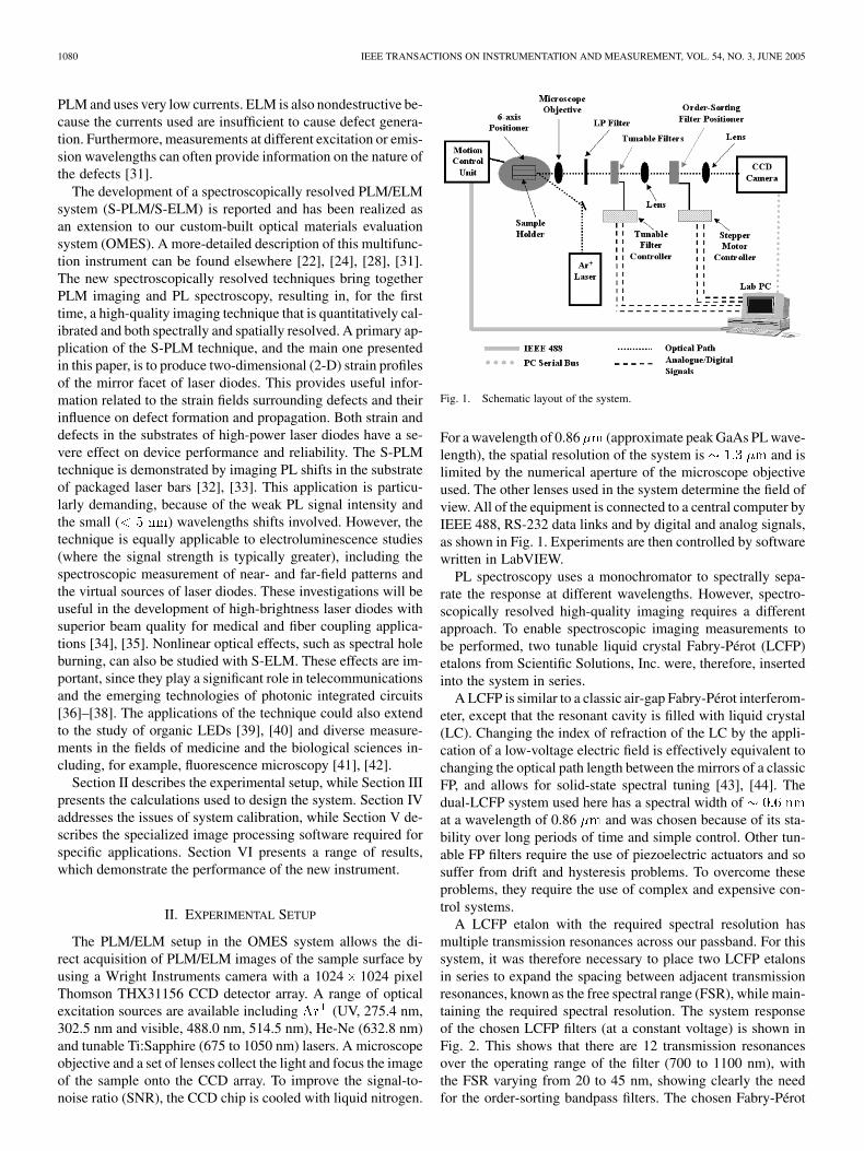
Fig. 1. Schematic layout of the system.
For a wavelength of 0.86 (approximate peak GaAs PL wave-length), the spatial resolution of the system is and islimited by the numerical aperture of the microscope objectiveused. The other lenses used in the system determine the field ofview. All of the equipment is connected to a central computer byIEEE 488, RS-232 data links and by digital and analog signals,as shown in Fig. 1. Experiments are then controlled by softwarewritten in LabVIEW.
PL spectroscopy uses a monochromator to spectrally sepa-rate the response at different wavelengths. However, spectro-scopically resolved high-quality imaging requires a differentapproach. To enable spectroscopic imaging measurements tobe performed, two tunable liquid crystal Fabry-Pérot (LCFP)etalons from Scientific Solutions, Inc. were, therefore, insertedinto the system in series.
A LCFP is similar to a classic air-gap Fabry-Pérot interferom-eter, except that the resonant cavity is filled with liquid crystal(LC). Changing the index of refraction of the LC by the appli-cation of a low-voltage electric field is effectively equivalent tochanging the optical path length between the mirrors of a classicFP, and allows for solid-state spectral tuning [43], [44]. Thedual-LCFP system used here has a spectral width ofat a wavelength of 0.86 and was chosen because of its sta-bility over long periods of time and simple control. Other tun-able FP filters require the use of piezoelectric actuators and sosuffer from drift and hysteresis problems. To overcome theseproblems, they require the use of complex and expensive con-trol systems.
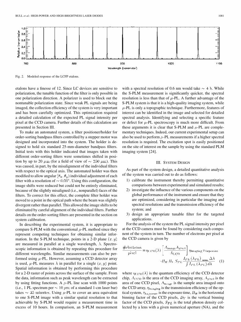
A LCFP etalon with the required spectral resolution hasmultiple transmission resonances across our passband. For thissystem, it was therefore necessary to place two LCFP etalonsin series to expand the spacing between adjacent transmissionresonances, known as the free spectral range (FSR), while main-taining the required spectral resolution. The system responseof the chosen LCFP filters (at a constant voltage) is shown inFig. 2. This shows that there are 12 transmission resonancesover the operating range of the filter (700 to 1100 nm), withthe FSR varying from 20 to 45 nm, showing clearly the needfor the order-sorting bandpass filters. The chosen Fabry-Pérot
BULL et al.: HIGH-POWER AND HIGH-BRIGHTNESS LASER DIODES 1081
Fig. 2. Modeled response of the LCFP etalons.
etalons have a finesse of 12. Since LC devices are sensitive topolarization, the tunable function of the filter is only possible inone polarization direction. A polarizer is used to block out thenontunable polarization state. Since weak PL signals are beingimaged, the collection efficiency of the system is very importantand has been carefully optimized. This optimization requireda detailed calculation of the expected PL signal intensity perpixel at the CCD camera. Further details of this calculation arepresented in Section III.
To make an automated system, a filter positioner/holder fororder-sorting bandpass filters controlled by a stepper motor wasdesigned and incorporated into the system. The holder is de-signed to hold six standard 25-mm-diameter bandpass filters.Initial tests with this holder indicated that images taken withdifferent order-sorting filters were sometimes shifted in posi-tion by up to 20 (for a field of view of ). Thiswas caused, in part, by the misalignment of the individual filterswith respect to the optical axis. The automated holder was thenmodified to allow angular individual adjustment of eachfilter with a resolution of . Using this configuration, theimage shifts were reduced but could not be entirely eliminated,because of the slightly misaligned (i.e., nonparallel) faces of thefilters. To correct for this effect, the complete filter holder wasmoved to a point in the optical path where the beam was slightlydivergent rather than parallel. This allowed the image shifts to beeliminated by careful alignment of the individual filters. Furtherdetails on the order-sorting filters are presented in the section onsystem calibration.
In describing the experimental system, it is appropriate tocompare S-PLM with the conventional -PL method since theyrepresent competing techniques for obtaining similar infor-mation. In the S-PLM technique, points in a 2-D planeare measured in parallel at a single wavelength, . Spectro-scopic information is obtained by repeating this procedure fordifferent wavelengths. Similar measurements can also be per-formed using -PL. However, assuming a CCD detector arrayis used, -PL measures in parallel for a single point.Spatial information is obtained by performing this procedurefor a 2-D raster of points across the surface of the sample. Fromthe data, information such as peak wavelength can be extractedby using fitting functions. A -PL line scan with 1000 points(i.e., 1 PL spectrum per of a standard 1-cm laser bar)takes . Using -PL to cover an area equivalentto one S-PLM image with a similar spatial resolution to thatachievable by S-PLM would require a measurement time inexcess of 10 hours. In comparison, an S-PLM measurement
with a spectral resolution of 0.6 nm would take . Whilethe S-PLM measurement is significantly quicker, the spectralresolution is less than that of -PL. A further advantage of theS-PLM system is that it is a high-quality imaging system, while
-PL is only a topographic technique. Furthermore, features ofinterest can be identified in the image and selected for detailedspectral analysis. Identifying and selecting a specific featureor defect for -PL spectroscopy is much more difficult. Fromthese arguments it is clear that S-PLM and -PL are comple-mentary techniques. Indeed, our current experimental setup canalso be used to perform -PL measurements if a higher spectralresolution is required. The excitation spot is easily positionedon the site of interest on the sample by using the standard PLMimaging system [24].
III. SYSTEM DESIGN
As part of the system design, a detailed quantitative analysisof the system was carried out to do as follows:
1) calibrate the instrument thereby permitting quantitativecomparisons between experimental and simulated results;
2) investigate the influence of the various components on theglobal performance of the instrument and ensure that theyare optimized, considering in particular the imaging andspectral resolutions and the transmission efficiency of thesystem; and
3) design an appropriate tunable filter for the targetedapplications.
For the analysis of the system the PL signal intensity per pixelat the CCD camera must be found by considering each compo-nent of the system in turn. The number of electrons per pixel atthe CCD camera is given by
(1)
where is the quantum efficiency of the CCD detectorchip, is the area of the CCD imaging array, is thearea of one CCD pixel, is the sample area imaged ontothe CCD array, is the transmission efficiency of the op-tical system, is the exposure time, is the horizontalbinning factor of the CCD pixels, is the vertical binningfactor of the CCD pixels, is the total photon density col-lected by a lens with a given numerical aperture (NA), and the
1082 IEEE TRANSACTIONS ON INSTRUMENTATION AND MEASUREMENT, VOL. 54, NO. 3, JUNE 2005
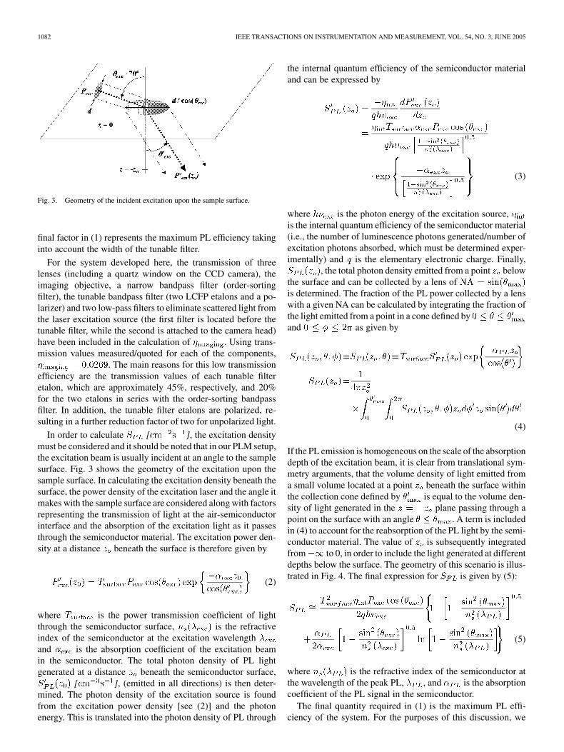
Fig. 3. Geometry of the incident excitation upon the sample surface.
final factor in (1) represents the maximum PL efficiency takinginto account the width of the tunable filter.
For the system developed here, the transmission of threelenses (including a quartz window on the CCD camera), theimaging objective, a narrow bandpass filter (order-sortingfilter), the tunable bandpass filter (two LCFP etalons and a po-larizer) and two low-pass filters to eliminate scattered light fromthe laser excitation source (the first filter is located before thetunable filter, while the second is attached to the camera head)have been included in the calculation of . Using trans-mission values measured/quoted for each of the components,
. The main reasons for this low transmissionefficiency are the transmission values of each tunable filteretalon, which are approximately 45%, respectively, and 20%for the two etalons in series with the order-sorting bandpassfilter. In addition, the tunable filter etalons are polarized, re-sulting in a further reduction factor of two for unpolarized light.
In order to calculate [ ], the excitation densitymust be considered and it should be noted that in our PLM setup,the excitation beam is usually incident at an angle to the samplesurface. Fig. 3 shows the geometry of the excitation upon thesample surface. In calculating the excitation density beneath thesurface, the power density of the excitation laser and the angle itmakes with the sample surface are considered along with factorsrepresenting the transmission of light at the air-semiconductorinterface and the absorption of the excitation light as it passesthrough the semiconductor material. The excitation power den-sity at a distance beneath the surface is therefore given by
(2)
where is the power transmission coefficient of lightthrough the semiconductor surface, is the refractiveindex of the semiconductor at the excitation wavelengthand is the absorption coefficient of the excitation beamin the semiconductor. The total photon density of PL lightgenerated at a distance beneath the semiconductor surface,
[ ], (emitted in all directions) is then deter-mined. The photon density of the excitation source is foundfrom the excitation power density [see (2)] and the photonenergy. This is translated into the photon density of PL through
the internal quantum efficiency of the semiconductor materialand can be expressed by
(3)
where is the photon energy of the excitation source,is the internal quantum efficiency of the semiconductor material(i.e., the number of luminescence photons generated/number ofexcitation photons absorbed, which must be determined exper-imentally) and is the elementary electronic charge. Finally,
, the total photon density emitted from a point belowthe surface and can be collected by a lens ofis determined. The fraction of the PL power collected by a lenswith a given NA can be calculated by integrating the fraction ofthe light emitted from a point in a cone defined byand as given by
(4)
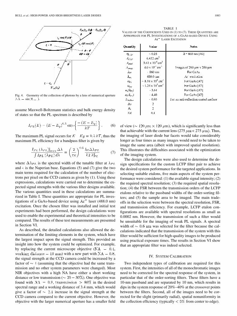
If the PL emission is homogeneous on the scale of the absorptiondepth of the excitation beam, it is clear from translational sym-metry arguments, that the volume density of light emitted froma small volume located at a point beneath the surface withinthe collection cone defined by is equal to the volume den-sity of light generated in the plane passing through apoint on the surface with an angle . A term is includedin (4) to account for the reabsorption of the PL light by the semi-conductor material. The value of is subsequently integratedfrom to 0, in order to include the light generated at differentdepths below the surface. The geometry of this scenario is illus-trated in Fig. 4. The final expression for is given by (5):
(5)
where is the refractive index of the semiconductor atthe wavelength of the peak PL, , and is the absorptioncoefficient of the PL signal in the semiconductor.
The final quantity required in (1) is the maximum PL effi-ciency of the system. For the purposes of this discussion, we
BULL et al.: HIGH-POWER AND HIGH-BRIGHTNESS LASER DIODES 1083
Fig. 4. Geometry of the collection of photons by a lens of numerical apertureNA = sin(� ).
assume Maxwell-Boltzmann statistics and bulk energy densityof states so that the PL spectrum is described by
(6)
The maximum PL signal occurs for , thus themaximum PL efficiency for a bandpass filter is given by
(7)
where is the spectral width of the tunable filter atand is the Naperian base. Equations (5) and (7) give the twomain terms required for the calculation of the number of elec-trons per pixel on the CCD camera as given by (1). Using theseexpressions, calculations were carried out to determine the ex-pected signal strengths with the various filter designs available.The various quantities used in these calculations are summa-rized in Table I. These quantities are appropriate for PL inves-tigations of a GaAs-based device using laser (488.0 nm)excitation. Once the chosen filter was installed and initial testexperiments had been performed, the design calculations wereused to enable the experimental and theoretical intensities to becompared. The results of these test measurements are presentedin Section VI.
As described, the detailed calculations also allowed the de-termination of the limiting elements in the system, which havethe largest impact upon the signal strength. This provided aninsight into how the system could be optimized. For example,by replacing the current microscope objective ( ,
) with a new part with ,the signal strength at the CCD camera could be increased by afactor of (assuming that the objective had the same trans-mission and no other system parameters were changed). MostNIR objectives with a high NA have either a short workingdistance or low transmission ( ). One objective wasfound with , in the desiredspectral range and a working distance of 3.4 mm, which wouldgive a factor of increase in the signal strength at theCCD camera compared to the current objective. However, theobjective with the larger numerical aperture has a smaller field
TABLE IVALUES OF THE COEFFICIENTS USED IN (1) TO (7). THESE QUANTITIES ARE
APPROPRIATE FOR PL INVESTIGATIONS OF A GAAS-BASED DEVICE USING
Ar LASER EXCITATION
of view ( ), which is significantly less thanthat achievable with the current lens (275 275 . Thus,the imaging of laser diode bar facets would take considerablylonger as four times as many images would need to be taken toimage the same area (albeit with improved spatial resolution).This illustrates the difficulties associated with the optimizationof the imaging system.
The design calculations were also used to determine the de-sign specifications for the custom LCFP filter pair to achievethe desired system performance for the targeted applications. Inselecting suitable etalons, five main aspects of the system per-formance were considered: (1) the available signal intensity; (2)the required spectral resolution; (3) the required spatial resolu-tion; (4) the FSR between the transmission orders of the LCFPetalons relative to the passband widths of the order-sorting fil-ters; and (5) the sample area to be imaged. The main trade-offs in the selection were between the spectral resolution, FSR,and transmission efficiency. For example, LCFP etalon con-figurations are available with spectral resolutions as small as0.0002 nm. However, the transmission of such a filter wouldbe unsuitable for the imaging of weak PL signals. A spectralwidth of was selected for the filter because the cal-culations indicated that the transmission of the system with thisfilter would be sufficient for high-quality images to be producedusing practical exposure times. The results in Section VI showthat an appropriate filter was indeed selected.
IV. SYSTEM CALIBRATION
Two independent types of calibration are required for thissystem. First, the intensities of all of the monochromatic imagesneed to be corrected for the spectral response of the system, inparticular that of the order-sorting filters. These filters have a10-nm passband and are separated by 10 nm, which results indips in the system response of 20%–40% at the crossover pointsbetween the filters. Second, all of the images need to be cor-rected for the slight (primarily radial), spatial nonuniformity inthe collection efficiency (typically from center to edge).
1084 IEEE TRANSACTIONS ON INSTRUMENTATION AND MEASUREMENT, VOL. 54, NO. 3, JUNE 2005
The spectral response of the system was measured using ahalogen lamp with a known emission spectrum. The beam fromthe lamp was focussed and reflected off a mirror mounted onthe sample positioner down the optical axis. A series of imagesat intervals of 0.5 nm were then taken using the CCD cameraat specific wavelengths determined by the tunable filter. Thisprocedure eliminates the need for an external spectrometer andalso calibrates for the spectral sensitivity of the CCD camera andnot just that of the optics. To determine the spectral response ofthe system, the integral intensity over all pixels of each imageis found. This is then corrected for the spectrum of the lampand normalized. This method gives an excellent SNR, since theSNR is proportional to the square root of the number of pixels.All pixels of an image are then multiplied by the normalizationfactor for the wavelength at which the image was taken.
The spatial nonuniformity in collection efficiency across in-dividual images was characterized by using a small point lightsource (an IR LED behind a 5- diameter pinhole) mountedon the six-axis positioner. Images were taken for a 2-D matrix ofpositions, which covered the size of the image. From the pointsin these images where the maximum intensity occurs, a 2-D plotcan be made of how the collection efficiency varies across theimage. This data is then used to correct the spatial nonunifor-mity in collection efficiency for all images. Software has beendeveloped to automate both of the calibration procedures andimage corrections.
V. IMAGE PROCESSING SOFTWARE
Specialized software is required to perform the image anal-ysis needed for a specific application. An individual image iscomprised of over a million pixels. In order to produce a full2-D strain profile, the software must first extract the local lu-minescence spectrum from each pixel in the image (or those inthe user defined region of interest). Then, it must fit a theoret-ical curve to the spectrum associated with each pixel, in orderto determine parameters such as the peak wavelength and theluminescence linewidth. These extracted parameters can thenbe plotted as 2-D topograms, giving a visual representation oftheir variation across the imaged region. In the results presentedin Section VI, the theoretical functions used for the fitting arequadratic and cubic polynomials.
The software is currently being expanded to include a largerrange of fitting functions suitable for a variety of applica-tions, including theoretical spectral lineshapes for spontaneousand stimulated emission. Both undoped and doped, bulk andquantum well (QW) material will be considered. Detailsof these theoretical functions will be presented in a futurepublication.
VI. DEMONSTRATION OF INSTRUMENT PERFORMANCE
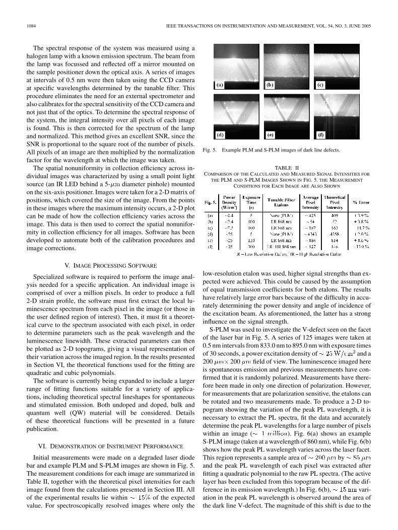
Initial measurements were made on a degraded laser diodebar and example PLM and S-PLM images are shown in Fig. 5.The measurement conditions for each image are summarized inTable II, together with the theoretical pixel intensities for eachimage found from the calculations presented in Section III. Allof the experimental results lie within of the expectedvalue. For spectroscopically resolved images where only the
Fig. 5. Example PLM and S-PLM images of dark line defects.
TABLE IICOMPARISON OF THE CALCULATED AND MEASURED SIGNAL INTENSITIES FOR
THE PLM AND S-PLM IMAGES SHOWN IN FIG. 5. THE MEASUREMENT
CONDITIONS FOR EACH IMAGE ARE ALSO SHOWN
low-resolution etalon was used, higher signal strengths than ex-pected were achieved. This could be caused by the assumptionof equal transmission coefficients for both etalons. The resultshave relatively large error bars because of the difficulty in accu-rately determining the power density and angle of incidence ofthe excitation beam. As aforementioned, the latter has a stronginfluence on the signal strength.
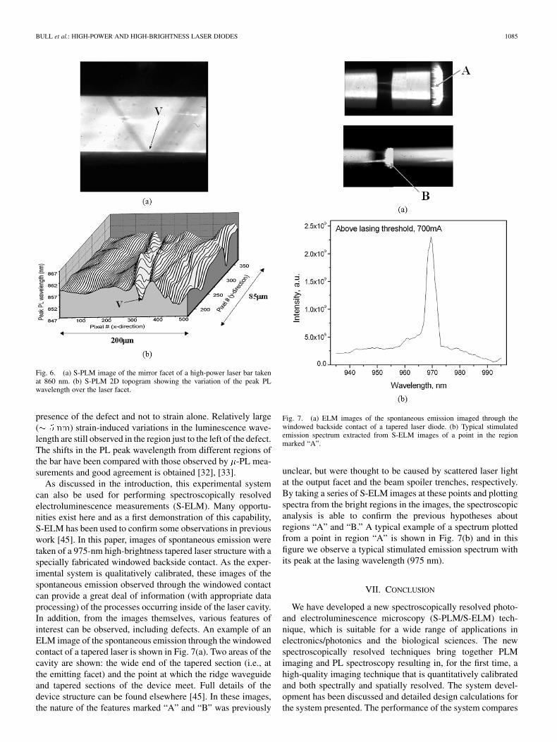
S-PLM was used to investigate the V-defect seen on the facetof the laser bar in Fig. 5. A series of 125 images were taken at0.5 nm intervals from 833.0 nm to 895.0 nm with exposure timesof 30 seconds, a power excitation density of and a200 200 field of view. The luminescence imaged hereis spontaneous emission and previous measurements have con-firmed that it is randomly polarized. Measurements have there-fore been made in only one direction of polarization. However,for measurements that are polarization sensitive, the etalons canbe rotated and two measurements made. To produce a 2-D to-pogram showing the variation of the peak PL wavelength, it isnecessary to extract the PL spectra, fit the data and accuratelydetermine the peak PL wavelengths for a large number of pixelswithin an image ( ). Fig. 6(a) shows an exampleS-PLM image (taken at a wavelength of 860 nm), while Fig. 6(b)shows how the peak PL wavelength varies across the laser facet.This region represents a sample area of byand the peak PL wavelength of each pixel was extracted afterfitting a quadratic polynomial to the raw PL spectra. (The activelayer has been excluded from this topogram because of the dif-ference in its emission wavelength.) In Fig. 6(b), vari-ation in the peak PL wavelength is observed around the area ofthe dark line V-defect. The magnitude of this shift is due to the
BULL et al.: HIGH-POWER AND HIGH-BRIGHTNESS LASER DIODES 1085
Fig. 6. (a) S-PLM image of the mirror facet of a high-power laser bar takenat 860 nm. (b) S-PLM 2D topogram showing the variation of the peak PLwavelength over the laser facet.
presence of the defect and not to strain alone. Relatively large( ) strain-induced variations in the luminescence wave-length are still observed in the region just to the left of the defect.The shifts in the PL peak wavelength from different regions ofthe bar have been compared with those observed by -PL mea-surements and good agreement is obtained [32], [33].
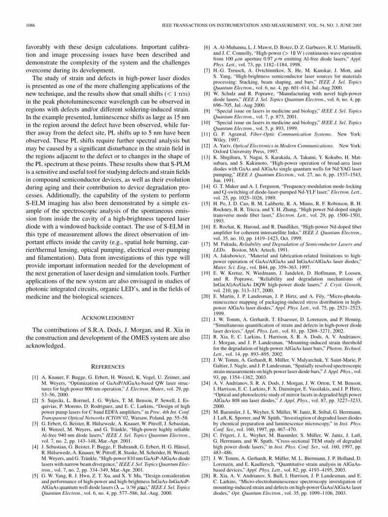
As discussed in the introduction, this experimental systemcan also be used for performing spectroscopically resolvedelectroluminescence measurements (S-ELM). Many opportu-nities exist here and as a first demonstration of this capability,S-ELM has been used to confirm some observations in previouswork [45]. In this paper, images of spontaneous emission weretaken of a 975-nm high-brightness tapered laser structure with aspecially fabricated windowed backside contact. As the exper-imental system is qualitatively calibrated, these images of thespontaneous emission observed through the windowed contactcan provide a great deal of information (with appropriate dataprocessing) of the processes occurring inside of the laser cavity.In addition, from the images themselves, various features ofinterest can be observed, including defects. An example of anELM image of the spontaneous emission through the windowedcontact of a tapered laser is shown in Fig. 7(a). Two areas of thecavity are shown: the wide end of the tapered section (i.e., atthe emitting facet) and the point at which the ridge waveguideand tapered sections of the device meet. Full details of thedevice structure can be found elsewhere [45]. In these images,the nature of the features marked “A” and “B” was previously
Fig. 7. (a) ELM images of the spontaneous emission imaged through thewindowed backside contact of a tapered laser diode. (b) Typical stimulatedemission spectrum extracted from S-ELM images of a point in the regionmarked “A”.
unclear, but were thought to be caused by scattered laser lightat the output facet and the beam spoiler trenches, respectively.By taking a series of S-ELM images at these points and plottingspectra from the bright regions in the images, the spectroscopicanalysis is able to confirm the previous hypotheses aboutregions “A” and “B.” A typical example of a spectrum plottedfrom a point in region “A” is shown in Fig. 7(b) and in thisfigure we observe a typical stimulated emission spectrum withits peak at the lasing wavelength (975 nm).
VII. CONCLUSION
We have developed a new spectroscopically resolved photo-and electroluminescence microscopy (S-PLM/S-ELM) tech-nique, which is suitable for a wide range of applications inelectronics/photonics and the biological sciences. The newspectroscopically resolved techniques bring together PLMimaging and PL spectroscopy resulting in, for the first time, ahigh-quality imaging technique that is quantitatively calibratedand both spectrally and spatially resolved. The system devel-opment has been discussed and detailed design calculations forthe system presented. The performance of the system compares
1086 IEEE TRANSACTIONS ON INSTRUMENTATION AND MEASUREMENT, VOL. 54, NO. 3, JUNE 2005
favorably with these design calculations. Important calibra-tion and image processing issues have been described anddemonstrate the complexity of the system and the challengesovercome during its development.
The study of strain and defects in high-power laser diodesis presented as one of the more challenging applications of thenew technique, and the results show that small shifts ( )in the peak photoluminescence wavelength can be observed inregions with defects and/or different soldering-induced strain.In the example presented, luminescence shifts as large as 15 nmin the region around the defect have been observed, while fur-ther away from the defect site, PL shifts up to 5 nm have beenobserved. These PL shifts require further spectral analysis butmay be caused by a significant disturbance in the strain field inthe regions adjacent to the defect or to changes in the shape ofthe PL spectrum at these points. These results show that S-PLMis a sensitive and useful tool for studying defects and strain fieldsin compound semiconductor devices, as well as their evolutionduring aging and their contribution to device degradation pro-cesses. Additionally, the capability of the system to performS-ELM imaging has also been demonstrated by a simple ex-ample of the spectroscopic analysis of the spontaneous emis-sion from inside the cavity of a high-brightness tapered laserdiode with a windowed backside contact. The use of S-ELM inthis type of measurement allows the direct observation of im-portant effects inside the cavity (e.g., spatial hole burning, car-rier/thermal lensing, optical pumping, electrical over-pumpingand filamentation). Data from investigations of this type willprovide important information needed for the development ofthe next generation of laser design and simulation tools. Furtherapplications of the new system are also envisaged in studies ofphotonic integrated circuits, organic LED’s, and in the fields ofmedicine and the biological sciences.
ACKNOWLEDGMENT
The contributions of S.R.A. Dods, J. Morgan, and R. Xia inthe construction and development of the OMES system are alsoacknowledged.
REFERENCES
[1] A. Knauer, F. Bugge, G. Erbert, H. Wenzel, K. Vogel, U. Zeimer, andM. Weyers, “Optimization of GaAsP/AlGaAs-based QW laser struc-tures for high power 800 nm operation,” J. Electron. Mater., vol. 29, pp.53–56, 2000.
[2] S. Sujecki, L. Borruel, J. G. Wykes, T. M. Benson, P. Sewell, I. Es-quivias, P. Moreno, D. Rodriguez, and E. C. Larkins, “Design of highpower pump lasers for C band EDFA amplifiers,” in Proc. 4th Int. Conf.Transparent Optical Networks ICTON’02, Warsaw, Poland, pp. 55–58.
[3] G. Erbert, G. Beister, R. Hülsewede, A. Knauer, W. Pitroff, J. Sebastian,H. Wenzel, M. Weyers, and G. Tränkle, “High-power highly reliableAl-free 940 nm diode lasers,” IEEE J. Sel. Topics Quantum Electron.,vol. 7, no. 2, pp. 143–148, Mar.-Apr. 2001.
[4] J. Sebastian, G. Beister, F. Bugge, F. Buhrandt, G. Erbert, H. G. Hänsel,R. Hülsewede, A. Knauer, W. Pitroff, R. Staske, M. Schröder, H. Wenzel,M. Weyers, and G. Tränkle, “High-power 810 nm GaAsP-AlGaAs diodelasers with narrow beam divergence,” IEEE J. Sel. Topics Quantum Elec-tron., vol. 7, no. 2, pp. 334–349, Mar.-Apr. 2001.
[5] G. W. Yang, R. J. Hwn, Z. T. Xu, and X. Y. Ma, “Design considerationand performance of high-power and high-brightness InGaAs-InGaAsP-AlGaAs quantum well diode lasers (� = 0:98�m),” IEEE J. Sel. TopicsQuantum Electron., vol. 6, no. 4, pp. 577–586, Jul.-Aug. 2000.
[6] A. Al-Muhanna, L. J. Mawst, D. Botez, D. Z. Garbuzov, R. U. Martinelli,and J. C. Connolly, “High-power (> 10W) continuous-wave operationfrom 100 �m aperture 0.97 �m emitting Al-free diode lasers,” Appl.Phys. Lett., vol. 73, pp. 1182–1184, 1998.
[7] H.-G. Treusch, A. Ovtchinnikov, X. He, M. Kanskar, J. Mott, andS. Yang, “High-brightness semiconductor laser sources for materialsprocessing: Stacking, beam shaping, and bars,” IEEE J. Sel. TopicsQuantum Electron., vol. 6, no. 4, pp. 601–614, Jul.-Aug 2000.
[8] W. Schulz and R. Poprawe, “Manufacturing with novel high-powerdiode lasers,” IEEE J. Sel. Topics Quantum Electron., vol. 6, no. 4, pp.696–705, Jul.-Aug 2000.
[9] “Special issue on lasers in medicine and biology,” IEEE J. Sel. TopicsQuantum Electron., vol. 7, p. 873, 2001.
[10] “Special issue on lasers in medicine and biology,” IEEE J. Sel. TopicsQuantum Electron., vol. 5, p. 893, 1999.
[11] G. P. Agrawal, Fiber-Optic Communication Systems. New York:Wiley, 1997.
[12] A. Yariv, Optical Electronics in Modern Communications. New York:Oxford University Press, 1997.
[13] K. Shigihara, Y. Nagai, S. Karakida, A. Takami, Y. Kokubo, H. Mat-subara, and S. Kakimoto, “High-power operation of broad-area laserdiodes with GaAs and AlGaAs single quantum wells for Nd:YAG laserpumping,” IEEE J. Quantum Electron., vol. 27, no. 6, pp. 1537–1543,Jun. 1991.
[14] G. T. Maker and A. I. Ferguson, “Frequency-modulation mode-lockingandQ-switching of diode-laser-pumped Nd-YLF laser,” Electron. Lett.,vol. 25, pp. 1025–1026, 1989.
[15] H. Po, J. D. Cao, B. M. Laliberte, R. A. Minns, R. F. Robinson, B. H.Rockney, R. R. Tricca, and Y. H. Zhang, “High power Nd-doped singletransverse mode fiber laser,” Electron. Lett., vol. 29, pp. 1500–1501,1993.
[16] E. Rochat, K. Haroud, and R. Dandliker, “High-power Nd-doped fiberamplifier for coherent intersatellite links,” IEEE J. Quantum Electron.,vol. 35, no. 10, pp. 1419–1423, Oct. 1999.
[17] M. Fukuda, Reliability and Degradation of Semiconductor Lasers andLEDs. Boston, MA: Artech, 1991.
[18] A. Jakubowicz, “Material and fabrication-related limitations to high-power operation of GaAs/AlGaAs and InGaAs/AlGaAs laser diodes,”Mater. Sci. Eng., vol. B44, pp. 359–363, 1997.
[19] E. W. Kretuz, N. Wiedmann, J. Jandeleit, D. Hoffmann, P. Loosen,and R. Poprawe, “Reliability and degradation mechanisms ofInGa(Al)As/GaAs DQW high-power diode lasers,” J. Cryst. Growth,vol. 210, pp. 313–317, 2000.
[20] E. Martin, J. P. Landesman, J. P. Hirtz, and A. Fily, “Micro-photolu-minescence mapping of packaging-induced stress distribution in high-power AlGaAs laser diodes,” Appl. Phys. Lett., vol. 75, pp. 2521–2523,1999.
[21] J. W. Tomm, A. Gerhardt, T. Elsaesser, D. Lorenzen, and P. Hennig,“Simultaneous quantification of strain and defects in high-power diodelaser devices,” Appl. Phys. Lett., vol. 81, pp. 3269–3271, 2002.
[22] R. Xia, E. C. Larkins, I. Harrison, S. R. A. Dods, A. V. Andrianov,J. Morgan, and J. P. Landesman, “Mounting-induced strain thresholdfor the degradation of high-power AlGaAs laser bars,” Photon. Technol.Lett., vol. 14, pp. 893–895, 2002.
[23] J. W. Tomm, A. Gerhardt, R. Müller, V. Malyarchuk, Y. Saint-Marie, P.Galtier, J. Nagle, and J. P. Landesman, “Spatially resolved spectroscopicstrain measurements on high-power laser diode bars,” J. Appl. Phys., vol.93, pp. 1354–1362, 2003.
[24] A. V. Andrianov, S. R. A. Dods, J. Morgan, J. W. Orton, T. M. Benson,I. Harrison, E. C. Larkins, F. X. Daiminger, E. Vassilakis, and J. P. Hirtz,“Optical and photoelectric study of mirror facets in degraded high powerAlGaAs 808 nm laser diodes,” J. Appl. Phys., vol. 87, pp. 3227–3233,2000.
[25] M. Baeumler, J. L. Weyher, S. Müller, W. Jantz, R. Stibal, G. Herrmann,J. Luft, K. Sporrer, and W. Späth, “Investiagtion of degraded laser diodesby chemical preparation and luminescence microscopy,” in Inst. Phys.Conf. Ser., vol. 160, 1997, pp. 467–470.
[26] C. Frigeri, J. L. Weyher, M. Baeumler, S. Müller, W. Jantz, J. Luft,G. Herrmann, and W. Spath, “Cross-sectional TEM study of degradedhigh power diode lasers,” in Inst. Phys. Conf. Ser., vol. 160, 1997, pp.483–486.
[27] J. W. Tomm, A. Gerhardt, R. Müller, M. L. Biermann, J. P. Holland, D.Lorenzen, and E. Kaulfersch, “Quantitative strain analysis in AlGaAs-based devices,” Appl. Phys. Lett., vol. 82, pp. 4193–4195, 2003.
[28] R. Xia, A. V. Andrianov, S. Bull, I. Harrison, J. P. Landesman, and E.C. Larkins, “Micro-electroluminescence spectroscopy investigation ofmounting-induced strain and defects on high-power GaAs/AlGaAs laserdiodes,” Opt. Quantum Electron., vol. 35, pp. 1099–1106, 2003.
BULL et al.: HIGH-POWER AND HIGH-BRIGHTNESS LASER DIODES 1087
[29] A. Klehr, G. Beister, G. Erbert, A. Klein, J. Maege, I. Rechenberg, J.Sebastian, H. Wenzel, and G. Tränkle, “Defect recognition via longitu-dinal mode analysis of high power fundamental mode and broad areaedge emitting laser diodes,” J. Appl. Phys., vol. 90, pp. 43–47, 2001.
[30] P. J. Bream, S. Bull, R. Xia, A. V. Andrianov, I. Harrison, and E. C.Larkins, “The influence of defects on the emission spectra of highpower laser diodes,” in Europhysics Conf. Abstracts, vol. 27E, CC2M,Conf. Lasers and Electro-Optics (CLEO) Europe, Munich, Germany,Jun. 2003.
[31] R. Xia, H. Xu, I. Harrison, B. Beaument, A. V. Andrianov, S. R. A.Dods, J. Morgan, and E. C. Larkins, “Spectrally resolved electrolumi-nescence microscopy and�-electroluminescence investigations of GaN-based LEDs,” J. Cryst. Growth, vol. 230, pp. 467–472, 2001.
[32] S. Bull, A. V. Andrianov, I. Harrison, and E. C. Larkins, “Develop-ment of a spectroscopically resolved photoluminescence microscopytechnique for studying strain and defects in high power laser diodes,”in Europhysics Conf. Abstracts, vol. 27E, CC4-04-MON, Conf. Lasersand Electro-Optics (CLEO) Europe, Munich, Germany, Jun. 2003.
[33] , “The study of strain and defects in high power laser diodes byspectroscopically resolved photoluminescence microscopy,” Eur. Phys.J. – Appl. Phys., vol. 27, pp. 469–473, 2004.
[34] O. P. Gough, U. Buckley, B. Corbett, and J. D. Lambkin, “Low-diver-gence laser structures for cost-effective fiber coupling applications,”IEEE J. Sel. Topics Quantum Electron., vol. 6, no. 4, pp. 571–576,Jul.-Aug. 2000.
[35] J. M. Verdiell, M. Ziari, and D. F. Welch, “Low-loss coupling of 980nm GaAs laser to cleaved singlemode fiber,” Electron. Lett., vol. 32, pp.1817–1818, 1996.
[36] A. Uskov, J. Mørk, and J. Mark, “Wave mixing in semiconductor laseramplifiers due to carrier heating and spectral-hole burning,” IEEE J.Quantum Electon., vol. 30, no. 8, pp. 1769–1781, Aug. 1994.
[37] R. Nietzke, P. Panknin, W. Elsässer, and E. O. Göbel, “Four-wave mixingin GaAs/AlGaAs semiconductor lasers,” IEEE J. Quantum Electon., vol.25, no. 6, pp. 1399–1406, Jun. 1989.
[38] C.-Y. Tsai and C.-Y. Tsai, “Carrier density depinning above thresholdin semiconductor lasers: Effects of carrier heating and spectral holeburning,” IEE Proc. Optoelectron., vol. 144, pp. 209–212, 1997.
[39] C. W. Tang and S. A. Van Slyke, “Organic electroluminescent diodes,”Appl. Phys. Lett., vol. 51, pp. 913–915, 1987.
[40] J. H. Bourroughes, D. D. C. Bradley, A. R. Brown, R. N. Marks, K.Mackay, R. H. Friend, P. L. Burns, and A. B. Holmes, “Light emittingdiodes based on conjugated polymers,” Nature, vol. 347, pp. 539–541,1990.
[41] K. A. Christensen, K. A. Bradley, M. D. Morris, and R. V. Morrison,“Raman imaging using a tunable dual-stage liquid-crystal Fabry-Perotinterferometer,” Appl. Spectrosc., vol. 49, pp. 1120–1125, 1995.
[42] H. R. Morris, C. C. Hoyt, and P. J. Treado, “Imaging spectrometers forfluorescence and Raman microscopy – Acousto-optic and liquid crystaltunable filters,” Appl. Spectrosc., vol. 48, pp. 857–866, 1994.
[43] W. J. Schneller, J. Noto, R. B. Kerr, and R. A. Doe, “Liquid crystalFabry-Perot etalons,” in Proc. SPIE, vol. 3355, 1998, pp. 877–883.
[44] J. Noto, Y. Betremieux, R. B. Kerr, H. Zhang, M. J. Taylor, S. Watchon,and M. Dorin, “Tandem-etalon tunable filter for NIR spectral imaging,”in Proc. SPIE, vol. 5157, 2003, pp. 178–189.
[45] S. Bull, J. G. Wykes, A. V. Andrianov, J. J. Lim, L. Borruel, S. Su-jecki, S. C. Auzanneau, M. Calligaro, M. Krakowski, I. Esquivias, andE. C. Larkins, “Imaging of spontaneous emission from 980 nm taperedlasers with windowed n-contacts,” Eur. Phys. J.– Appl. Phys., vol. 27,pp. 455–459, 2004.
[46] THX31156 CCD Data Sheet and Calibration Data Provided by WrightInstruments.
[47] M. R. Brozel and G. E. Stillman, Properties of Gallium Arsenide, 3rded. London, U.K.: INSPEC IEE, 1996, pp. 207–213.
Stephen Bull (S’01) received the M.Eng. degreein electronic engineering with German (first classhonors) and the Ph.D. degree from the Universityof Nottingham in 2001 and 2004, respectively.His Ph.D. research was in the characterization anddegradation of high-power and high-brightness semi-conductor lasers, using spectroscopically resolvedimaging techniques.
His current research interests include the numer-ical modeling of laser diodes, spectroscopic imagingtechniques for the characterization of laser diodes and
the validation of simulation tools and the degradation dynamics of high-powerlaser bars.
Alexander V. Andrianov received the M.Sc. degreein optoelectronics with honors from Leningrad Elec-trotechnical Institute, Russia, in 1979 and the Ph.D.degree in physics of semiconductors from Ioffe Phys-ical Technical Institute, Russia, in 1983.
He is currently a Senior Research Fellow withIoffe Physical Technical Institute, St Petersburg,where his research interests include the optics oflow-dimensional systems, nonequilibrium phe-nomena in semiconductors and semiconductordevices, and wide bandgap materials. He was a
Research Associate with the University of Nottingham from 1996 to 1998and again in 2002. During this time, his research activities included theestablishment of a multifunctional optical laboratory for the characterizationsemiconductor devices, photo- and electroluminescence studies of high-powerlaser diodes and investigations of the optical properties of the GaAs:N andGaN:As material systems.
Ian Harrison received the B.Sc. degree from theUniversity of Nottingham, Nottingham, U.K., andthe Ph.D. degree from the University of Manchester,Manchester, U.K.
Since 1987, he has been with the University of Not-tingham. He recently spent a year with the Univer-sity of California, Santa Barbara, where he worked onhigh-speed digital circuits and devices. He has pub-lished extensively on the electrical and optical prop-erties of semiconductors devices and materials.
Dr. Harrison received the Royal Academy of En-gineering’s Engineering Foresight Award in 2001.
Michael Dorin received the B.S. degree in as-tronomy from Boston University, Boston, MA, in1994.
He has been an Applications Engineer, as well asthe Director of Sales and Marketing, at Scientific So-lutions, Inc. since May of 2001. He has known andworked with Dr. Noto and Dr. Kerr since 1990.
Robert B. Kerr received the B.S. degree in physicsfrom Ohio University, Athens, OH, in 1979, the M.S.and Ph.D. degrees, both in atmospheric science, fromThe University of Michigan, in 1981 and 1986, re-spectively.
He joined Scientific Solutions, Inc. (SSI) in 1997,serving originally as Director of Research, and since2000, as Chief Executive Officer. He was a memberof the technical staff at the Aerospace Corporation,El Segundo, CA, in 1987. He was a Professor ofAstronomy at Boston University, Boston, MA, from
1988 to 1997.Dr. Kerr is currently serving his second term on the Arecibo Observatory
Scientific Advisory Committee.
1088 IEEE TRANSACTIONS ON INSTRUMENTATION AND MEASUREMENT, VOL. 54, NO. 3, JUNE 2005
John Noto received the B.S. degree in physics and as-tronomy from the University of Rochester, Rochester,NY, the M.S. degree in physics from Tufts Univer-sity, and the Ph.D. degree in astronomy/space physicsfrom Boston University, Boston, MA.
He is the President and Co-Founder of ScientificSolutions, Inc. (SSI), as well as the inventor of theLiquid Crystal Fabry-Perot interferometer as devel-oped by SSI. He has more than 10 years of experi-ence in optical research and development, focused onnarrow-band spectroscopy and interferometry.
Eric Larkins (S’92–M’89) received the B.S. degreein electrical engineering from Cornell University,Ithaca, NY, in 1980 and the M.S. and Ph.D. degrees,both in electrical engineering from Stanford Uni-versity in 1985 and 1991, respectively. He pursuedthe Ph.D. degree research on light-emitting het-erostructure thyristors and molecular-beam epitaxy,receiving full support from 1985 as a Kodak Fellow.
He joined the School of Electrical and ElectronicEngineering, University of Nottingham, U.K., asLecturer in 1994 and was appointed Professor of
Optoelectronics in 2002. From 1991 to 1994, he was a visiting scientist withthe Fraunhofer Institute for Applied Solid State Physics, Freiburg, Germany,where he worked on high-speed laser diodes, optical modulators, and MSM andintersubband photodetectors. His current research interests include high-powerlaser diodes, functional photonics, and new optical materials.