Embed Size (px)
Citation preview
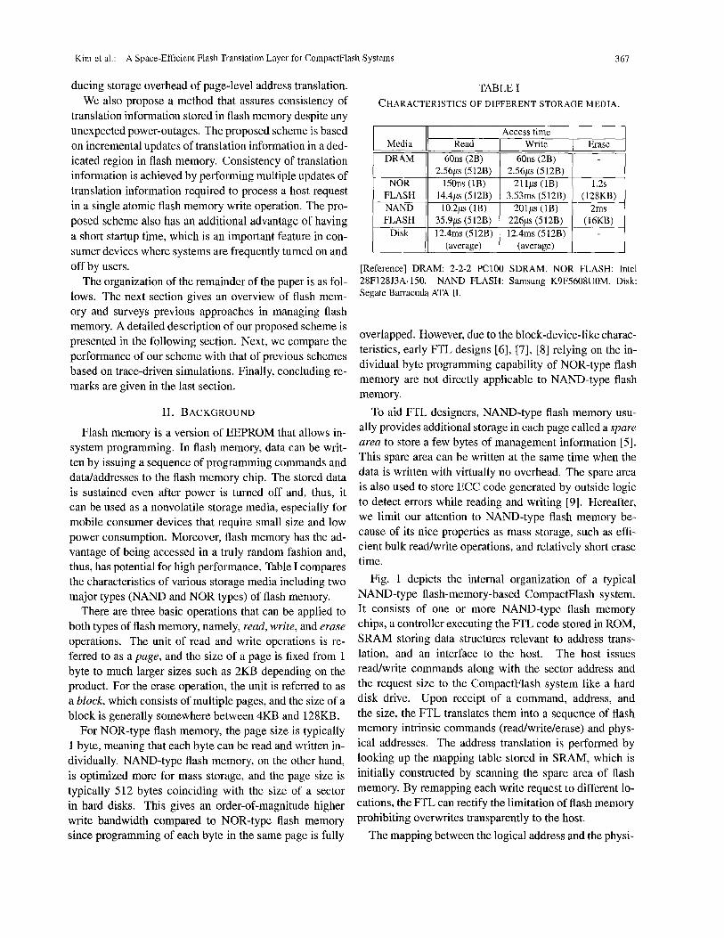
366 IEEE Transactions on Consumer Electronics, Vol. 48, No. 2, MAY 2002
A SPACE-EFFICIENT FLASH TRANSLATION LAYER FOR COMPACTFLASH SYSTEMS Jesung Kim, Jong Min Kim, Sam H. Noh, Sang Lyul Min and Yookun Cho
Abstract-Flash memory is becoming increasingly im- portant as nonvolatile storage for mobile consumer elec- tronics due to its low power consumption and shock resis- tance. However, it imposes technical challenges in that a write should be preceded by an erase operation, and that this erase operation can be performed only in a unit much larger than the write unit. To address these technical hur- dles, an intermediate software layer called a flash transla- tion layer (FTL) is generally employed to redirect logical ad- dresses from the host system to physical addresses in flash memory. Previous approaches have performed this address translation at the granularity of either a write unit (page) or an erase unit (block). In this paper, we propose a novel FTL design that combines the two different granularities in address translation. This is motivated by the idea that coarse grain address translation lowers resources required to maintain translation information, which is crucial in mo- bile consumer products for cost and power consumption reasons, while fine grain address translation is efficient in handling small size writes. Performance evaluation based on trace-driven simulation shows that the proposed scheme significantly outperforms previously proposed approaches.
Index Terms-Flash memory, NAND-type flash memory, FTL, CompactFlash, address translation.
I. INTRODUCTION
ECENmY, mobile computing devices such as PDAs R and digital cameras have become very popular. These mobile devices impose different design require- ments such as small size, lightweight, low power con- sumption, and shock resistance. These new requirements necessitate redesign of various components of the under- lying computer system. In particular, design of nonvolatile storage subsystems for mobile devices is one of the most challenging areas since traditional magnetic disks are gen- erally lacking in power efficiency and shock resistance due to their mechanical nature.
Flash memory has been recognized as an attractive
Jesung Kim, Sang Lyul Min, and Yookun Cho are with the School of Computer Science and Engineering, Seoul National University, Korea. E-mail: jskim @archi.snu,ac.kl; [email protected]; [email protected]. kr:
Jong Min Kim is with Samsung Electronics, Korea. Email: jmkim @archi.snu.ac.kr:
Sam H. Noh is with the School of Information and Computer Engi- neering, Hong-Ik University, Korea. E-mail: samhnoh@ hongik.ac.kr:
long-term storage media for mobile computers because of its superiority in small size, shock resistance, and low power consumption [l], [2]. Moreover, as there is no me- chanical delay involved, random access is possible thereby providing excellent performance. These properties make flash-memory-based storage subsystems that emulate hard disks very popular for secondary storage of mobile com- puters (e.g., CompactFlash [3], and SmartMedia [4]). It is anticipated that as the capacity of flash memory grows [5] , the use of flash memory will become more prevalent, coexisting with hard disks or even replacing hard disks outright even in conventional computer systems.
Flash memory, however, has several characteristics that make difficult straightforward replacement of magnetic disks. First, a write in flash memory should be preceded by an erase operation, which takes an order of magnitude longer than a write operation. Second, erase operations can only be performed in a much larger unit than the write operation. This implies that, for an update of even a single byte, an erase operation as well as restoration of a large amount of data would be required. This not only degrades the potential performance significantly, but also gives rise to an integrity problem since data may be lost if the power goes down unexpectedly during the restoration process, which may happen frequently in hand-held devices.
To address these problems, an intermediate software layer called ajlash translation layer (FTL) has been em- ployed between the host application and flash memory [6], [7]. The FTL redirects each write request from the host to an empty location in flash memory that has been erased in advance. Although this technique rectifies the aforemen- tioned limitation of erase-before-write, it comes at a price of extra flash memory operations to prepare empty loca- tions and extra storage to maintain the address translation information, the amount of which varies significantly de- pending on the management algorithm.
In this paper, we propose a novel FTL design aimed at mass storage CompactFlash systems [3]. The main motivation of the proposed FTL is that coarse grain ad- dress translation lowers management overhead whereas fine grain address translation is efficient in handling small size writes. The proposed scheme combines the two dif- ferent granularities in address translation to allow efficient handling of write requests smaller than a block while re-
Contributed Paper
Manuscript received April 10, 2002 0098 3063/00 $10.00 2002 IEEE
Kim et al.: A Space-Efficient Flash Translation Layer for CompactFlash Systems 3 67
Media DRAM
ducing storage overhead of page-level address translation. We also propose a method that assures consistency of
translation information stored in flash memory despite any unexpected power-outages. The proposed scheme is based on incremental updates of translation information in a ded- icated region in flash memory. Consistency of translation information is achieved by performing multiple updates of translation information required to process a host request in a single atomic flash memory write operation. The pro- posed scheme also has an additional advantage of having a short startup time, which is an important feature in con- sumer devices where systems are frequently turned on and off by users.
The organization of the remainder of the paper is as fol- lows. The next section gives an overview of flash mem- ory and surveys previous approaches in managing flash memory. A detailed description of our proposed scheme is presented in the following section. Next, we compare the performance of our scheme with that of previous schemes based on trace-driven simulations. Finally, concluding re- marks are given in the last section.
11. BACKGROUND
Flash memory is a version of EEPROM that allows in- system programming. In flash memory, data ran be writ- ten by issuing a sequence of programming commands and dataladdresses to the flash memory chip. The stored data is sustained even after power is turned off and, thus, it can be used as a nonvolatile storage media, especially for mobile consumer devices that require small size and low power consumption. Moreover, flash memory has the ad- vantage of being accessed in a truly random fashion and, thus, has potential for high performance. Table I compares the characteristics of various storage media including two major types (NAND and NOR types) of flash memory.
There are three basic operations that can be applied to both types of flash memory, namely, read, write, and erase operations. The unit of read and write operations is re- ferred to as a page, and the size of a page is fixed from 1 byte to much larger sizes such as 2KB depending on the product. For the erase operation, the unit is referred to as a bEock, which consists of multiple pages, and the size of a block is generally somewhere between 4KB and 128KB.
For NOR-type flash memory, the page size is typically 1 byte, meaning that each byte can be read and written in- dividually. NAND-type flash memory, on the other hand, is optimized more for mass storage, and the page size is typically 512 bytes coinciding with the size of a sector in hard disks. This gives an order-of-magnitude higher write bandwidth compared to NOR-type Aash memory since programming of each byte in the same page is fully
Read Write 1 Erase 60ns(2B) I 60ns(2B) I
TABLE I CHARACTERISTICS OF DIFFERENT STORAGE MEDIA.
NOR FLASH NAND FLASH
Disk
I II Access time I
2 S 6 p (512B) 2 . 5 6 ~ (512B)
1 4 . 4 ~ (512B) 3.53ms (512B) (128KB) 1 0 . 2 ~ (IB) 2 0 1 p (1B) 2ms
3 5 . 9 ~ (512B) 2 2 6 p (512B) (16KB) 12.4ms (512B) 12.4ms (512B)
(average) (average)
15011s (1B) 2 1 1 p ( l e ) 1.2s
overlapped. However, due to the block-device-like charac- teristics, early FTL designs [6], [7], [8] relying on the in- dividual byte programming capability of NOR-type flash memory are not directly applicable to NAND-type flash memory.
To aid FTL designers, NAND-type flash memory usu- ally provides additional storage in each page called a spare area to store a few bytes of management information [5] . This spare area can be written at the same time when the data is written with virtually no overhead. The spare area is also used to store ECC code generated by outside logic to detect errors while reading and writing [9]. Hereafter, we limit our attention to NAND-type flash memory be- cause of its nice properties as mass storage, such as effi- cient bulk read/write operations, and relatively short erase time.
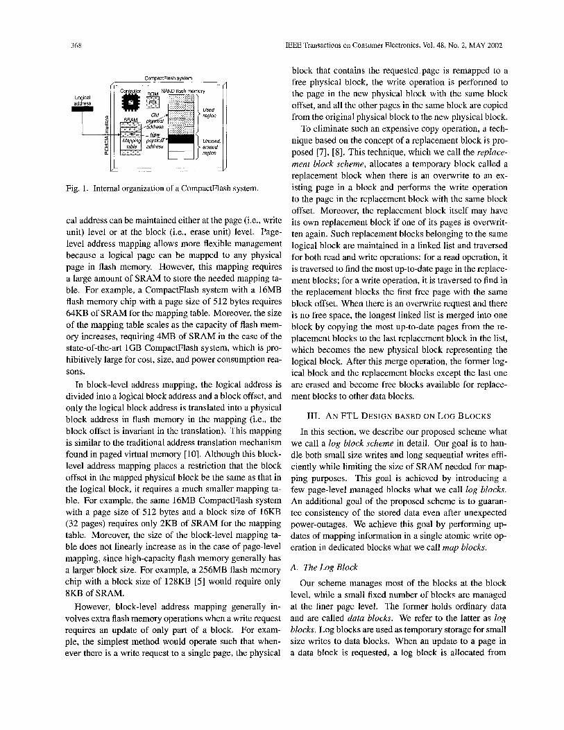
Fig. 1 depicts the internal organization of a typical NAND-type flash-memory-based CompactFlash system. It consists of one or more NAND-type flash memory chips, a controller executing the FTL code stored in ROM, SRAM storing data structures relevant to address trans- lation, and an interface to the host. The host issues r edwr i t e commands along with the sector address and the request size to the CompactFlash system like a hard disk drive. Upon receipt of a command, address, and the size, the FTL translates them into a sequence of flash memory intrinsic commands (read/write/erase) and phys- ical addresses. The address translation is performed by looking up the mapping table stored in SRAM, which is initially constructed by scanning the spare area of flash memory. By remapping each write request to different lo- cations, the FTL can rectify the limitation of flash memory prohibiting overwrites transparently to the host.
The mapping between the logical address and the physi-
368
CompactFlash system
Logical address
T I
SRAM
address 1 I 1 erased region ,
Fig. 1. Internal organization of a CompactFlash system.
cal address can be maintained either at the page (Le., write unit) level or at the block (Le., erase unit) level. Page- level address mapping allows more flexible management because a logical page can be mapped to any physical page in flash memory. However, this mapping requires a large amount of SRAM to store the needed mapping ta- ble. For example, a CompactFlash system with a 16MB flash memory chip with a page size of 512 bytes requires 64KB of SRAM for the mapping table. Moreover, the size of the mapping table scales as the capacity of flash mem- ory increases, requiring 4MB of SRAM in the case of the state-of-the-art 1GB CompactFlash system, which is pro- hibitively large for cost, size, and power consumption rea- sons.
In block-level address mapping, the logical address is divided into a logical block address and a block offset, and only the logical block address is translated into a physical block address in flash memory in the mapping (Le., the block offset is invariant in the translation). This mapping is similar to the traditional address translation mechanism found in paged virtual memory [ 101. Although this block- level address mapping places a restriction that the block offset in the mapped physical block be the same as that in the logical block, it requires a much smaller mapping ta- ble. For example, the same 16MB CompactFlash system with a page size of 512 bytes and a block size of 16KB (32 pages) requires only 2- of SRAM for the mapping table. Moreover, the size of the block-level mapping ta- ble does not linearly increase as in the case of page-level mapping, since high-capacity flash memory generally has a larger block size. For example, a 256MB flash memory chip with a block size of 128KB [5] would require only 8KB of SRAM.
However, block-level address mapping generally in- volves extra flash memory operations when a write request requires an update of only part of a block. For exam- ple, the simplest method would operate such that when- ever there is a write request to a single page, the physical
IEEE Transactions on Consumer Electronics, Vol. 48, No. 2, MAY 2002
block that contains the requested page is remapped to a free physical block, the write operation is performed to the page in the new physical block with the same block offset, and all the other pages in the same block are copied from the original physical block to the new physical block.
To eliminate such an expensive copy operation, a tech- nique based on the concept of a replacement block is pro- posed [7], [SI. This technique, which we call the replace- ment block scheme, allocates a temporary block called a replacement block when there is an overwrite to an ex- isting page in a block and performs the write operation to the page in the replacement block with the same block offset. Moreover, the replacement block itself may have its own replacement block if one of its pages is ovenvrit- ten again. Such replacement blocks belonging to the same logical block are maintained in a linked list and traversed for both read and write operations: for a read operation, it is traversed to find the most up-to-date page in the replace- ment blocks; for a write operation, it is traversed to find in the replacement blocks the first free page with the same block offset. When there is an overwrite request and there is no free space, the longest linked list is merged into one block by copying the most up-to-date pages from the re- placement blocks to the last replacement block in the list, which becomes the new physical block representing the logical block. After this merge operation, the former log- ical block and the replacement blocks except the last one are erased and become free blocks available for replace- ment blocks to other data blocks.
111. AN FTL DESIGN BASED ON LOG BLOCKS
In this section, we describe our proposed scheme what we call a log block scheme in detail. Our goal is to han- dle both small size writes and long sequential writes effi- ciently while limiting the size of SRAM needed for map- ping purposes. This goal is achieved by introducing a few page-level managed blocks what we call log blocks. An additional goal of the proposed scheme is to guaran- tee consistency of the stored data even after unexpected power-outages. We achieve this goal by performing up- dates of mapping information in a single atomic write op- eration in dedicated blocks what we call map blocks.
A. The Log Block
Our scheme manages most of the blocks at the block level, while a small fixed number of blocks are managed at the finer page level. The former holds ordinary data and are called data blocks. We refer to the latter as log blocks. Log blocks are used as temporary storage for small size writes to data blocks. When an update to a page in a data block is requested, a log block is allocated from
Kim et al.: A Space-Efficient Flash Translation Layer for CompactFlash Systems 369
the pool of free blocks that have been erased in advance and the update is performed to the log block incrementally from the first page. On each write, the logical address of the page is also stored in the spare area that is associated with each page. Note that the write to the spare area can be performed simultaneously as the corresponding page is written with virtually no overhead.
In this setting, for a read request the log blocks have to be checked to see if the requested page is present. If the requested page is present in the log block, it is provided to the host system, shadowing the corresponding page in the data block. To make this checking process efficient, we maintain a page-level mapping table for each log block in SRAM. This table is constructed on system startup by scanning the logical address stored in the spare area of each page in the log blocks, and updated on every write to point to the up-to-date pages. Note that pages in the log block whose logical pages have been updated multi- ple times do not require any special handling because, by scanning the log block backward from the last page, we can always identify the page that contains the up-to-date copy of a logical page.
B. Merge Operation
Once a log block is allocated for a data block, write re- quests to the data block can be performed in the log block without any extra operations, until all the pages in the log block are consumed. When this happens, we reclaim the log block by merging it with the corresponding data block.
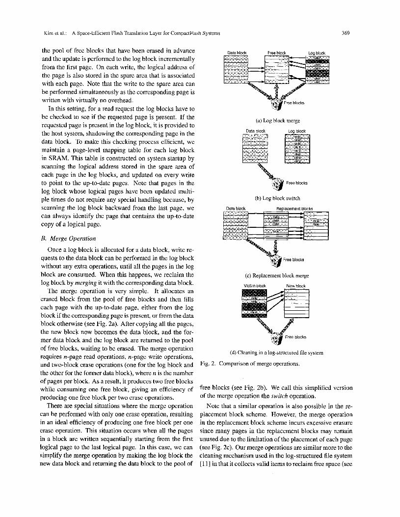
The merge operation is very simple. It allocates an erased block from the pool of free blocks and then fills each page with the up-to-date page, either from the log block if the corresponding page is present, or from the data block otherwise (see Fig. 2a). After copying all the pages, the new block now becomes the data block, and the for- mer data block and the log block are returned to the pool of free blocks, waiting to be erased. The merge operation requires n-page read operations, n-page write operations, and two-block erase operations (one for the log block and the other for the former data block), where n is the number of pages per block. As a result, it produces two free blocks while consuming one free block, giving an efficiency of producing one free block per two erase operations.
There are special situations where the merge operation can be performed with only one erase operation, resulting in an ideal efficiency of producing one free block per one erase operation. This situation occurs when all the pages in a block are written sequentially starting from the first logical page to the last logical page. In this case, we can simplify the merge operation by making the log block the new data block and returning the data block to the pool of
Data block Free block Log block
(a) Log block merge
Data block
(b) Log block switch
Data block Replacement blocks
(c) Replacement block merge
Victim block New block
(d) Cleaning in a log-structured file system
Fig. 2. Comparison of merge operations.
free blocks (see Fig. 2b). We call this simplified version of the merge operation the switch operation.
Note that a similar operation is also possible in the re- placement block scheme. However, the merge operation in the replacement block scheme incurs excessive erasure since many pages in the replacement blocks may remain unused due to the limitation of the placement of each page (see Fig. 2c). Our merge operations are similar more to the cleaning mechanism used in the log-structured file system [ 111 in that it collects valid items to reclaim free space (see
370 IEEE Transactions on Consumer Electronics, Vol. 48, No. 2, MAY 2002
map
map
Data block
Log block Free block
Mapping
fragments ' fable
Fig. 3. Mapping information management.
Fig. 2d). The difference lies in the fact that our scheme re- stricts pages in a log block to be from the same data block, and efficiency of the merge operation is independent of the number of valid pages in the log block. In contrast, the cleaning operation in the log-structured file system con- sumes a portion of an empty block to relocate valid pages in the block being cleaned, and thus the efficiency is in- versely proportional to the number of valid pages, which depends on the utilization as well as the policy of selecting a block to be cleaned [l], [ l l ] , [12], [131, [141.
C. The Map block
Both the merge operation and the switch operation change the mapping of the data block and thus, require an update to the mapping information. In previous schemes, mapping information is stored for each pageblock in the associated spare area in the form of logical address tags. Basically, these tags provide physical-to-logical reverse translation information and needs to be reconstructed as a conventional logical-to-physical mapping table. This requires scanning of the entire space of flash memory to collect logical address tags scattered across all the pageshlocks, which is prohibitively time- and power- consuming especially in NAND-type flash memory where reading a few bytes costs virtually the same as reading a page. Moreover, the mapping table is generally required to be present in SRAM as a whole.
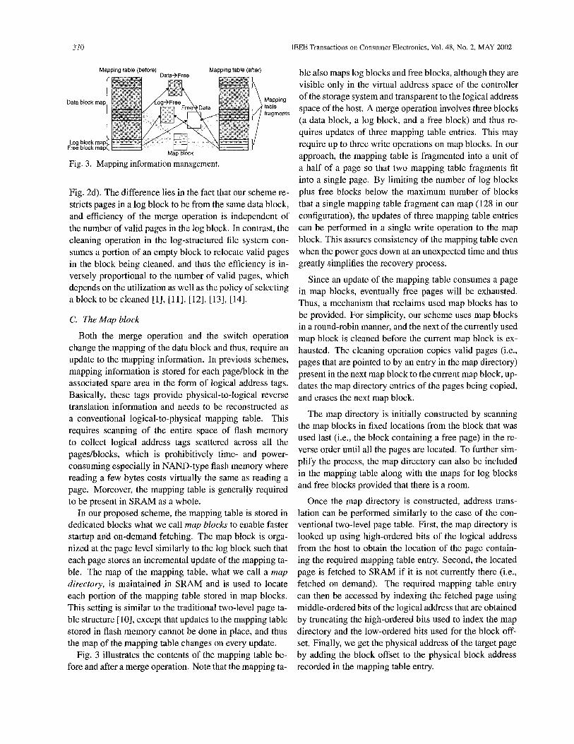
In our proposed scheme, the mapping table is stored in dedicated blocks what we call map blocks to enable faster startup and on-demand fetching. The map block is orga- nized at the page level similarly to the log block such that each page stores an incremental update of the mapping ta- ble. The map of the mapping table, what we call a map directory, is maintained in SRAM and is used to locate each portion of the mapping table stored in map blocks. This setting is similar to the traditional two-level page ta- ble structure [lo], except that updates to the mapping table stored in flash memory cannot be done in place, and thus the map of the mapping table changes on every update.
Fig. 3 illustrates the contents of the mapping table be- fore and after a merge operation. Note that the mapping ta-
ble also maps log blocks and free blocks, although they are visible only in the virtual address space of the controller of the storage system and transparent to the logical address space of the host. A merge operation involves three blocks (a data block, a log block, and a free block) and thus re- quires updates of three mapping table entries. This may require up to three write operations on map blocks. In our approach, the mapping table is fragmented into a unit of a half of a page so that two mapping table fragments fit into a single page. By limiting the number of log blocks plus free blocks below the maximum number of blocks that a single mapping table fragment can map (128 in our configuration), the updates of three mapping table entries can be performed in a single write operation to the map block. This assures consistency of the mapping table even when the power goes down at an unexpected time and thus greatly simplifies the recovery process.
Since an update of the mapping table consumes a page in map blocks, eventually free pages will be exhausted. Thus, a mechanism that reclaims used map blocks has to be provided. For simplicity, our scheme uses map blocks in a round-robin manner, and the next of the currently used map block is cleaned before the current map block is ex- hausted. The cleaning operation copies valid pages (i.e., pages that are pointed to by an entry in the map directory) present in the next map block to the current map block, up- dates the map directory entries of the pages being copied, and erases the next map block.
The map directory is initially constructed by scanning the map blocks in fixed locations from the block that was used last (i.e., the block containing a free page) in the re- verse order until all the pages are located. To further sim- plify the process, the map directory can also be included in the mapping table along with the maps for log blocks and free blocks provided that there is a room.
Once the map directory is constructed, address trans- lation can be performed similarly to the case of the con- ventional two-level page table. First, the map directory is looked up using high-ordered bits of the logical address from the host to obtain the location of the page contain- ing the required mapping table entry. Second, the located page is fetched to SRAM if it is not currently there (Le., fetched on demand). The required mapping table entry can then be accessed by indexing the fetched page using middle-ordered bits of the logical address that are obtained by truncating the high-ordered bits used to index the map directory and the low-ordered bits used for the block off- set. Finally, we get the physical address of the target page by adding the block offset to the physical block address recorded in the mapping table entry.
Kim et al.: A Space-Efficient Flash Translation Layer for CompactFlash Systems 37 1
D. Atomicity of Host Requests
Flash-memory-based storage subsystems such as Com- pactFlash systems should maintain a consistent state even when there is an unexpected power-outage since, for ex- ample, users of a digital camera are allowed to remove the CompactFlash card from the digital camera at any time. Therefore, assuring consistency of internal data structures is an important requirement of any FTL.
In our proposed scheme, updates of meta-data (Le., the mapping table) are performed in a single atomic write op- eration as explained in the previous subsection. This as- sures that the meta-data stored in flash memory is always consistent, even in the case where a write operation to the map block fails due to an unexpected power outage. As briefly explained in Section 11, failure of write operations can be detected by checking ECC code stored in the spare area for each page. Thus, simply ignoring the page with an ECC error leads to reconstruction of the mapping table to the state exactly the same as before the interrupted write operation is issued.
Furthermore, we can handle a long sequential write re- quest from the host as a single atomic operation by delay- ing updates of mapping information until all the data from the host is received completely. The received data is stored temporarily in free blocks and switched to data blocks si- multaneously by updating the corresponding mapping ta- ble entries after all the data are stored. The update of the mapping table effectively commits the host request. Note that this modification does not degrade per€ormance. In fact, it improves performance since several updates of the mapping table are piggy-backed to a single write opera- tion. This feature is useful in simplifying file-system level consistency management since large data structures can be updated in a single atomic operation [15], [16].
There are a few cases that need to be handled more care- fully. First, if small size writes are directed to a log block and are interrupted in the middle, partial results can be seen by the host after a restart. This case can be addressed by introducing a bit for each page in the log block that in- dicates the end of a sequence of a write. That is, a page in a log block with the bit cleared is regarded as valid only when it is followed by a page with the bit set. Second, a sufficient number of free blocks need to be available for buffering the data from the host, or otherwise atomicity of the request cannot be guaranteed. For this case, the file system has a choice of letting the storage system ei- ther to return an error or to take the risk. Finally, a se- quence of blocks involved in a request may extend beyond the boundary of a map fragment, and thus requires two sequential writes to the map block before it can be com-
Fig. 4. CompactFlash prototype system.
mitted. This situation can be addressed by using a simi- lar bit flag indicating the end of a sequence of a write as explained above. Using this method, atomicity of higher- level transactions may be envisioned similarly to the pre- vious approaches in the hard-disk-based storage hierarchy [151, ~161.
IV. PERFORMANCE EVALUATION
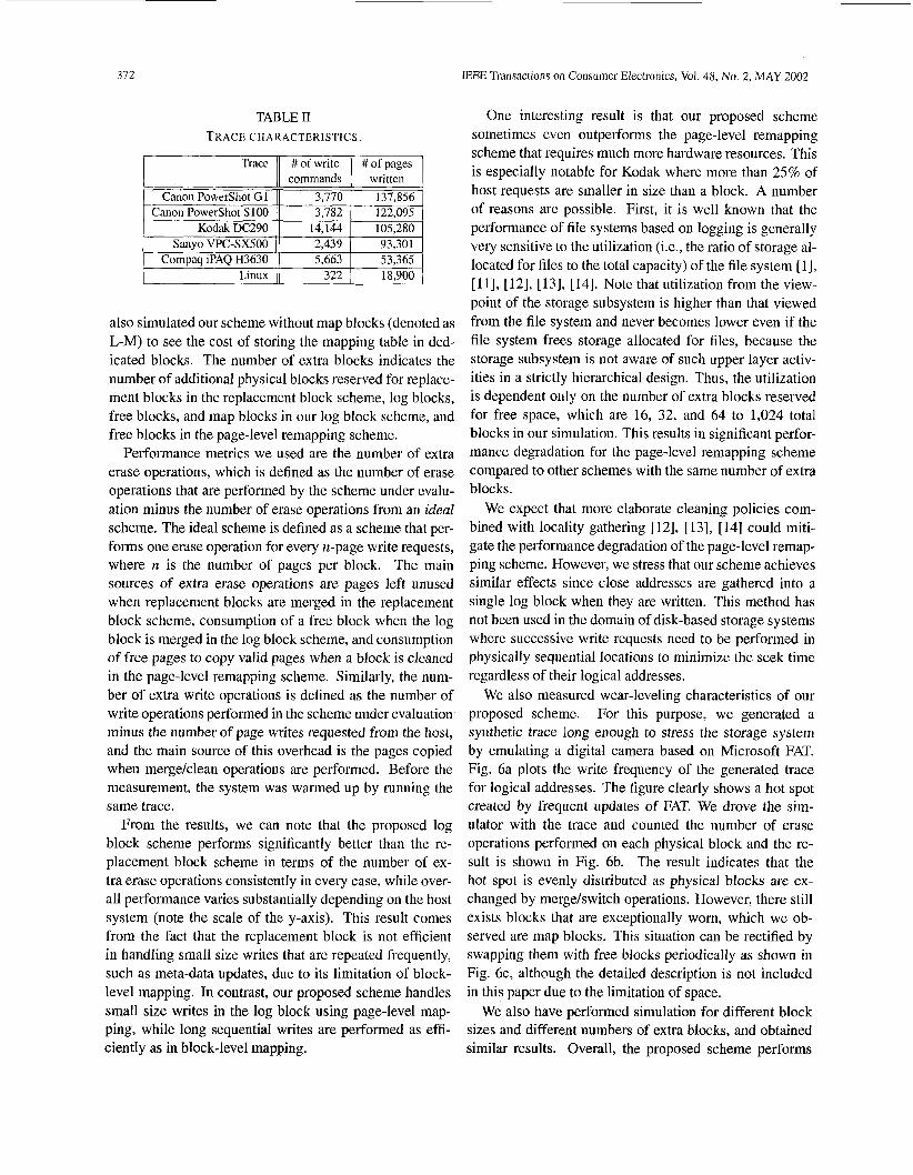
To evaluate the proposed FTL design, we implemented the scheme in a prototype 16MB CompactFlash storage system shown in Fig. 4. Also, to compare the perfor- mance of the proposed log block scheme with that of the replacement block scheme and the page-level remapping scheme, we developed a simulator for each of the three schemes and performed trace-driven simulations. The traces that were used to drive the simulation were obtained by plugging the prototype into four different digital cam- eras (Canon Powershot GI, Canon PowerShot S100, Ko- dak DC290, and Sanyo VPC-SXSOO), a PDA (Compaq iPAQ H3630), and a notebook computer running the Linux operating system. For this purpose, the firmware in the prototype was slightly modified to enable trace gathering.
For the workload of the digital cameras, we operated the cameras in their usual mode: taking, browsing, and erasing pictures. For the PDA, we ran typical applica- tions including web synchronization, MP3 file download and play, and file copying. Finally, we used the Andrew benchmark [17] for the workload of the Linux notebook computer. The characteristics of the traces in terms of the number of write commands and the aggregate number of pages written are given in Table 11. The traces include many sequential accesses as well as hot spots that are ac- cessed intensively. Sequential access patterns are usually from storing user data such as image files, while the hot spots are from updates of meta-data of the file system (Mi- crosoft FAT and Linux Ext2) due to creation/deletion of files.
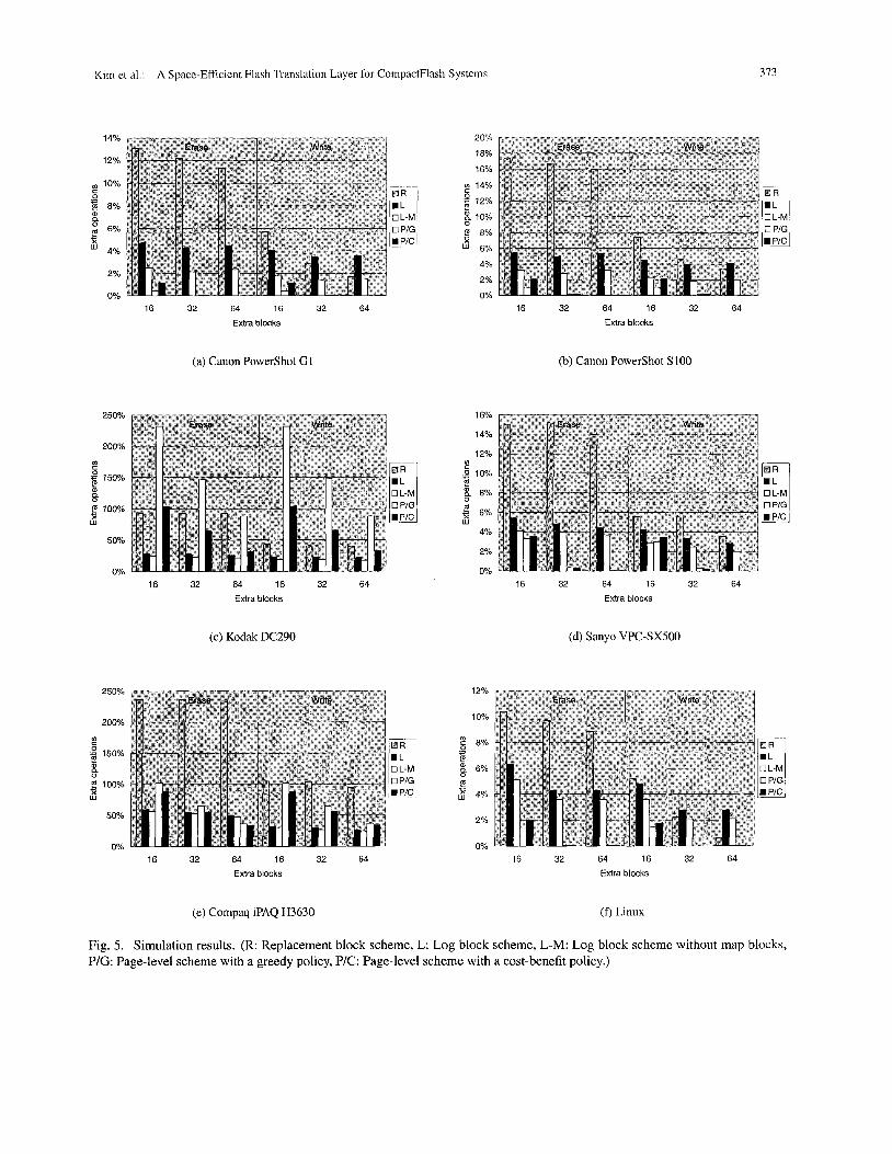
Fig. 5 shows the results for the three schemes simu- lated including two versions of the page-level remapping scheme with a greedy policy [ l l ] (denoted as P/G) and with a cost-benefit policy [ l l ] , [13] (denoted as P/C). We
372 IEEE Transactions on Consumer Electronics, Vol. 48, No. 2, MAY 2002
Trace
Canon PowerShot G1 Canon Powershot SlOO
Kodak DC290 sanyo vPc-sx500
Compaq iPAQ H3630 Linux
TABLE I1 TRACE CHARACTERISTICS.
#ofwrite #ofpages ’ commands written is especially notable for Kodak where more than 25% of
host requests are smaller in size than a block. A number of reasons are possible. First, it is well known that the performance of file systems based on logging is generally very sensitive to the utilization (Le., the ratio of storage al- located for files to the total capacity) of the file system [ 11,
3,770 137,856 3,782 122,095
14,144 105,280 2,439 93,301 5,663 53,365
322 18,900
One interesting result is that our proposed scheme sometimes even outperforms the page-level remapping
also simulated our scheme without map blocks (denoted as L-M) to see the cost of storing the mapping table in ded- icated blocks. The number of extra blocks indicates the number of additional physical blocks reserved for replace- ment blocks in the replacement block scheme, log blocks, free blocks, and map blocks in our log block scheme, and free blocks in the page-level remapping scheme.
Performance metrics we used are the number of extra erase operations, which is defined as the number of erase operations that are performed by the scheme under evalu- ation minus the number of erase operations from an ideal scheme. The ideal scheme is defined as a scheme that per- forms one erase operation for every n-page write requests, where n is the number of pages per block. The main sources of extra erase operations are pages left unused when replacement blocks are merged in the replacement block scheme, consumption of a free block when the log block is merged in the log block scheme, and consumption of free pages to copy valid pages when a block is cleaned in the page-level remapping scheme. Similarly, the num- ber of extra write operations is defined as the number of write operations performed in the scheme under evaluation minus the number of page writes requested from the host, and the main source of this overhead is the pages copied when mergeklean operations are performed. Before the measurement, the system was warmed up by running the same trace.
From the results, we can note that the proposed log block scheme performs significantly better than the re- placement block scheme in terms of the number of ex- tra erase operations consistently in every case, while over- all performance varies substantially depending on the host system (note the scale of the y-axis). This result comes from the fact that the replacement block is not efficient in handling small size writes that are repeated frequently, such as meta-data updates, due to its limitation of block- level mapping. In contrast, our proposed scheme handles small size writes in the log block using page-level map- ping, whiIe long sequential writes are performed as effi- ciently as in block-level mapping.
point of the storage subsystem is higher than that viewed from the file system and never becomes lower even if the file system frees storage allocated for files, because the storage subsystem is not aware of such upper layer activ- ities in a strictly hierarchical design. Thus, the utilization is dependent only on the number of extra blocks reserved for free space, which are 16, 32, and 64 to 1,024 total blocks in our simulation. This results in significant perfor- mance degradation for the page-level remapping scheme compared to other schemes with the same number of extra blocks.
We expect that more elaborate cleaning policies com- bined with locality gathering [12], [13], [14] could miti- gate the performance degradation of the page-level remap- ping scheme. However, we stress that our scheme achieves similar effects since close addresses are gathered into a single log block when they are written. This method has not been used in the domain of disk-based storage systems where successive write requests need to be performed in physically sequential locations to minimize the seek time regardless of their logical addresses.
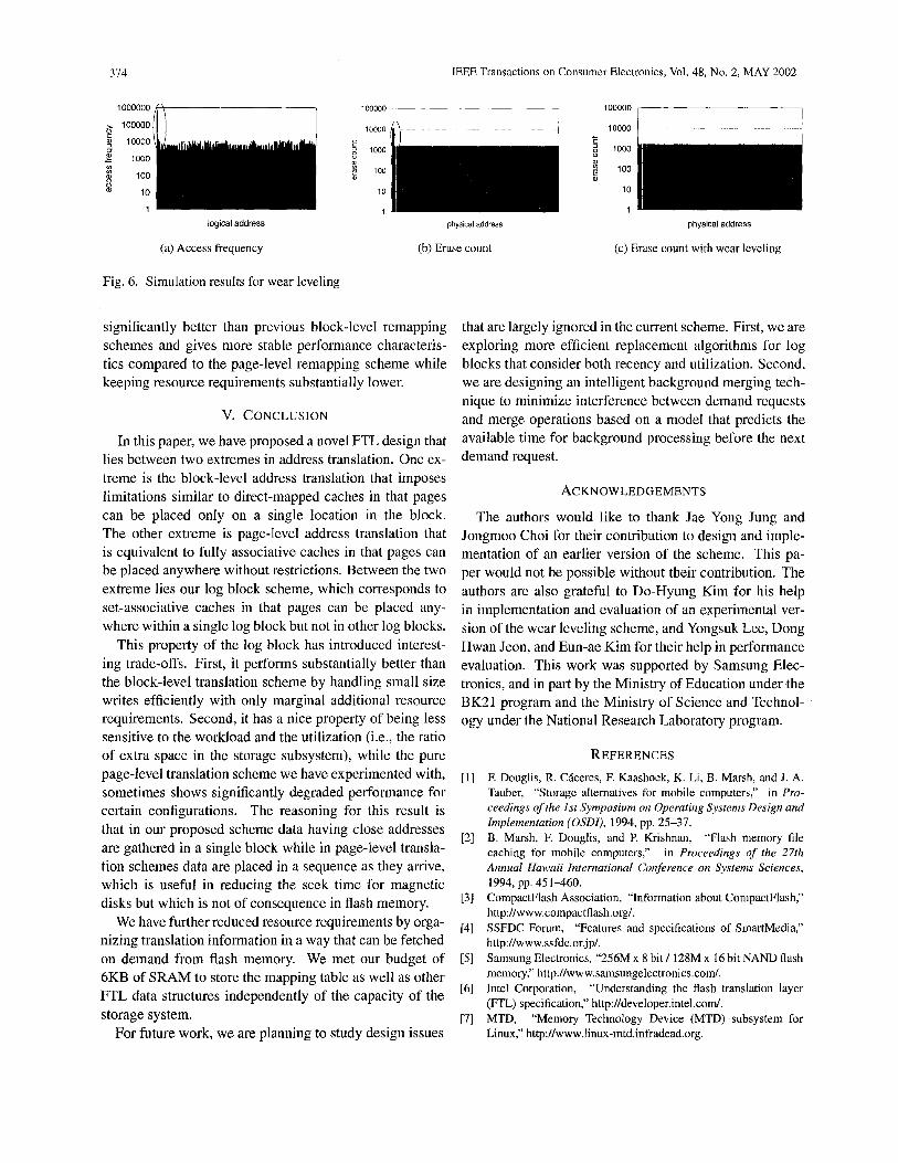
We also measured wear-leveling characteristics of our proposed scheme. For this purpose, we generated a synthetic trace long enough to stress the storage system by emulating a digital camera based on Microsoft FAT. Fig. 6a plots the write frequency of the generated trace for logical addresses. The figure clearly shows a hot spot created by frequent updates of FAT. We drove the sim- ulator with the trace and counted the number of erase operations performed on each physical block and the re- sult is shown in Fig. 6b. The result indicates that the hot spot is evenly distributed as physical blocks are ex- changed by mergekwitch operations. However, there still exists blocks that are exceptionally worn, which we ob- served are map blocks. This situation can be rectified by swapping them with free blocks periodically as shown in Fig. 6c, although the detailed description is not included in this paper due to the limitation of space.
We also have performed simulation for different block sizes and different numbers of extra blocks, and obtained similar results. Overall, the proposed scheme performs
Kiln et al.: A Space-Efficient Flash Translation Layer for CompactFlash Systems 313
14%
12%
u) 10%
p 8%
C
m
.-
.- a
6%
4%
2%
0% 16 32 64 16 32 64
Extra blocks
(a) Canon Powershot G1
16 32 64 16 32 64 Extra blocks
(b) Canon PowerShot SlOO
250% 16%
14%
12% 200%
Lo
s 150% e 8 2 100% 6% W W
4%
2%
0% 0%
50%
16 32 64 16 32 64
Extra blocks
16 32 64 16 32 64
Extra blocks
(c ) Kodak DC290 (d) Sanyo VPC-SXSOO
250% 12%
10% 200% u)
2 150% E a
6 100% e W 3 4%
2%
0% 0%
50%
16 32 64 16 32 64 Extra blocks
16 32 64 16 32 64
Extra blocks
(e) Compaq iPAQ H3630 (f) Linux
Fig. 5. Simulation results. (R: Replacement block scheme, L: Log block scheme, L-M: Log block scheme without map blocks, P/G: Page-level scheme with a greedy policy, PIC: Page-level scheme with a cost-benefit policy.)
374
logical address
(a) Access frequency
Fig. 6. Simulation results for wear leveling
IEEE Transactions on Consumer Electronics, Vol. 48, No. 2, MAY 2002
physical address
(b) Erase count
significantly better than previous block-level remapping schemes and gives more stable performance characteris- tics compared to the page-level remapping scheme while keeping resource requirements substantially lower.
V. CONCLUSION
In this paper, we have proposed a novel FTL design that lies between two extremes in address translation. One ex- treme is the block-level address translation that imposes limitations similar to direct-mapped caches in that pages can be placed only on a single location in the block. The other extreme is page-level address translation that is equivalent to fully associative caches in that pages can be placed anywhere without restrictions. Between the two extreme lies our log block scheme, which corresponds to set-associative caches in that pages can be placed any- where within a single log block but not in other log blocks.
This property of the log block has introduced interest- ing trade-offs. First, it performs substantially better than the block-level translation scheme by handling small size writes efficiently with only marginal additional resource requirements. Second, it has a nice property of being less sensitive to the workload and the utilization &e., the ratio of extra space in the storage subsystem), while the pure page-level translation scheme we have experimented with, sometimes shows significantly degraded performance for certain configurations. The reasoning for this result is that in our proposed scheme data having close addresses are gathered in a single block while in page-level transla- tion schemes data are placed in a sequence as they arrive, which is useful in reducing the seek time for magnetic disks but which is not of consequence in flash memory.
We have further reduced resource requirements by orga- nizing translation information in a way that can be fetched on demand from flash memory. We met our budget of 6KB of SRAM to store the mapping table as well as other FTL data structures independently of the capacity of the storage system.
For future work, we are planning to study design issues
physical address
(c) Erase count with wear leveling
that are largely ignored in the current scheme. First, we are exploring more efficient replacement algorithms for log blocks that consider both recency and utilization. Second, we are designing an intelligent background merging tech- nique to minimize interference between demand requests and merge operations based on a model that predicts the available time for background processing before the next demand request.
ACKNOWLEDGEMENTS
The authors would like to thank Jae Yong Jung and Jongmoo Choi for their contribution to design and imple- mentation of an earlier version of the scheme. This pa- per would not be possible without their contribution. The authors are also grateful to Do-Hyung Kim for his help in implementation and evaluation of an experimental ver- sion of the wear leveling scheme, and Yongsuk Lee, Dong Hwan Jeon, and Eun-ae Kim for their help in performance evaluation. This work was supported by Samsung Elec- tronics, and in part by the Ministry of Education under the BK21 program and the Ministry of Science and Technol- ogy under the National Research Laboratory program.
REFERENCES F. Douglis, R. Ciceres, F. Kaashoek, K. Li, B. Marsh, and J. A. Tauber, “Storage altematives for mobile computers,” in Pro- ceedings of the 1st Symposium on Operating Systems Design and Implementation (OSDI), 1994, pp. 25-37. B. Marsh, F. Douglis, and P. Krishnan, ‘‘Flash memory file caching for mobile computers,” in Proceedings of the 27th Annual Hawaii International Conference on Systems Sciences, 1994, pp. 451-460. CompactFlash Association, “Information about CompactFlash,” http://www.compactflash.org/. SSFDC Forum, “Features and specifications of SmartMedia,” http://www.ssfdc.or.jp/. Samsung Electronics, “256M x 8 bit / 128M x 16 bit NAND flash memory,” http://www.samsungelectronics.coml. Intel Corporation, “Understanding the flash translation layer (FTL) specification,” http://developer.intel.com/. MTD, “Memory Technology Device (MTD) subsystem for Linux,” http://www.linux-mtd.infradead.org.
Kiln et a1 : A Space-Efficient Flash Translation Layer for CompactFlash Systems 375
[8] A. Ban, “Flash file system,” United States Patent, no. 5,404,485, Sam H. Noh received the BS degree in April 1995. computer engineering from Seoul National
[9] E. Harari, R. D. Norman, and S. Mehrotra, “Flash EEPROM Univeristy, Korea, in 1986, and the PhD degree system,” United States Patent, no. 5,602,987, Feb. 1997. from the University of Maryland at College
[IO] A. Silberschatz and P. B. Calvin, Operating System Concepts, Park in 1993. He held a visiting faculty position John Wiley & Sons, Inc., New York, NY, 1998. at George Waslungton University from 1993
[ 111 M. Rosenblum and J. Ousterhout, “The design and implementa- to 1994 before joining Hong-Ik University in tion of a log-structured file system,” ACM Transactions on Coni- Seoul, Korea, where he is now an associate puter Systems, vol. IO, no. 1, pp. 26-52, Feb. 1992. professor in the School of Information and M. Wu and W. Zwaenepoel,.’ “eNVy: A Non-Volatile, main memory storage system,” in Proceedings of the Sixth Inter- national Conference on Architectural Support for Programming Languages and Operating Systems (ASPLOS-6), 1994, pp. 86- 97. A. Kawaguchi, S. Nishioka, and H. Motoda, “A flash-memory based file system,” in Proceedings of the USENIX 199.5 Winter Technical Conference, 1995, pp. 155-164. M.-L. Chiang, P. C. H. Lee, and R.-C. Chang, “Using data clustering to improve cleaning performance for flash memory,” Software: Practice and Experience, vol. 29, no. 3, pp. 267-290, March 1999. C. Chao, R. English, D. Jacobson, A. Stepanov, and J. Wilkes, “Mime: A high performance parallel storage device with strong recovery guarantees,” Tech. Rep. HPL-CSP-92-9, Hewlett- Packard Laboratories, CA, 1992. W. de Jonge, M. E Kaashoek, and W. C. Hsieh, “The logical disk: A new approach to improving file systems,” in Proceedings of the 14th ACM Symposium on Operating Systems Principles (SOSP ’93), 1993, pp. 15-28. J. K. Howard, S. Menees, D. Nichols, M. Satyanarayanan, N. Sidebotham, and M. West, “Scale and performance in a dis- tributed file system,” ACM Transaction on Computer Systems, vol. 6, no. 1, pp. 51-81, Feb. 1988.
Jesung Kim received the BS, MS, and PhD de- grees in computer engineering from Seoul Na- tional University, Korea, in 1991, 1993, and 1998, respectively. He was an research engi- neer at the Information & Telecommunications R&D Center of Hyundai Electronics, Korea, from 1998 to 2000. He is currently a post- doctoral researcher in the School of Computer Science and Engineering, Seoul National Uni-
versity. His research interests include computer architecture, embed- ded systems, memory management, and Bluetooth-based personal area networking. Dr. Kim is a member of the IEEE.
Computer Engineering. His current research intercsts include parallel and distributed systems, VO issues in operating systems, and real-time systems. Dr. Noh is a member of the IEEE and the ACM.
Sang Lyul Min received the BS and MS de- grees in computer engineenng, both from Seoul National University, Korea, in 1983 and 1985, respectively. In 1985, he was awarded a Full- bright scholarship to pursue graduate studies at the University of Washington. He received the MS and PhD degrees in computer science from the University of Washington, Seattle, in 1988 and 1989, respectively. He is currently a pro-
fessor in the School of Computer Science and Engineering, Seoul Na- tional University, Korea. Previously, he was an assistant professor in the Department of Computer Engineering, Pusan National University, Korea, from 1989 to 1992, and a visiting scientist at the IBM T. J. Watson Research Center, Yorktown Heights, New York, from 1989 to 1990. He has served on a number of commttees of tcchnical confer- ences and workshops, including the IEEE Real-Time Systems Sympo- sium (RTSS), the IEEE Real-Time Technology and Applications Sym- posium (RTAS), the ACM SICPLAN Workshop on Languages, Com- pilers, and Tools for Embedded Systems (LCTES), and the Intema- tional Conference on Distributed Computing Systems (ICDCS). He is also a member of the editorial board of the IEEE Transactions on Com- puters. His research interests include computer architecture, real-time computing, parallel processing, and computer performance evaluation. Dr. Min is a member of the IEEE.
Yookun Cho received the BS degree from Seoul National University, Korea, in 1971 and the PhD degree in computer science from the University of Minnesota at Minneapolis in 1978. He has been with the School of Computer Science and Engineering since 1979, where he is currently a professor. He was a visiting assistant professor at the University of Minnesota dunng 1985 and a director of Educational and Research Comput-
Jong Min Kim received the BS degree in com- puter engineering from Pusan National Univer- sity, Korea, in 1992, and the MS degree in com- puter engineering from Seoul National Univer- sity, Korea, in 1994. He is a PhD candidate of Seoul National University. Currently, he is with Samsung Electronics, Korea. His research in- terests include memory management in operat- ing systems, buffer management in database sys-
tems, and cache management in storage systems. He is a member of the IEEE.
ing Center at Seoul National University from 1993 to 1995. He was a member of the program committee of the IPPS/SPDP’98 in 1997 and the Intemational Conference on High-Performance Computing from 1995 to 1997. His research interests include operating systems, algo- rithms, system security, and fault-tolerant computing systems. Dr. Cho is a member of the IEEE.