Embed Size (px)
Citation preview
IEEE JOURNAL OF SOLID-STATE CIRCUITS, VOL. 41, NO. 7, JULY 2006 1513
A GSM-GPRS/UMTS FDD-TDD/WLAN802.11a-b-g Multi-Standard Carrier
Generation SystemAdil Koukab, Yu Lei, Student Member, IEEE, and Michel J. Declercq, Fellow, IEEE
Abstract—A compact carrier generation system enabling properinteroperability among quad-band GSM, WCDMA (FDD andTDD), and WLAN (802.11a/b/g) standards is developed. Theimplementation is achieved in 0.25- m BiCMOS-SiGe process.The measured tuning range is higher that 1 GHz (3.05 to 4.1 GHz)exceeding the specifications by 25%. The voltage-controlled os-cillator (VCO) exhibits a phase noise of 118 and 125 dBc/Hzmeasured, respectively, at 400 kHz and 1 MHz offsets whiledrawing 2.5 mA from 2.5 V supply. The measured phase noise at400 kHz offset of the PCS/DCS output local-oscillator (LO) signaland the GSM output LO signal is, respectively, 124 dBc/Hz and
130 dBc/Hz.
Index Terms—Analog front-end (AFE), frequency synthesizer,GSM, multi-standard, phase noise, phase-locked loop (PLL),UMTS, voltage-controlled oscillator (VCO), wireless communica-tions, WLAN.
I. INTRODUCTION
THE fundamental requirements driving the wireless com-munication market today are the global mobility and the
wide range of the proposed services. These two forces haveresulted in two complementary mature technologies: WLAN(IEEE 802.11a/b/g) for high bandwidth, hot spot local cov-erage; and cellular handset for voice communication with widearea coverage. Both of them have recently experienced a shiftfrom single system connectivity to multi-system connectivity.Single chip systems fully compliant with the IEEE 802.11a/b/gstandards were recently presented [1]–[3]. In the case of cellularsystems, the interoperability is motivated by the fact that the3G (UMTS) will coexist with 2–2.5G (GSM/GPRS). Varioussolutions were proposed to integrate these standards in thesame chip [4], [5]. On the other hand, the modern handsetsare designed to handle more and more high-data-rate appli-cations such as games, graphics, audio and video, etc. Theserequirements can be fulfilled by the convergence of cellular2G–3G standards and WLAN technology in the same handset[6]. However, without an intensive innovation effort, the pro-cessing complexity, memory and power consumption of suchsystems will be so huge that they will never result in a viable
Manuscript received November 15, 2005; revised January 31, 2006. Thiswork was supported in part by the Swiss Office Fédérale de l’Education et de laScience within the European ST project MuMor under contract IST-2001-3461.
The authors are with Ecole Polytechnique Fédérale de Lausanne (EPFL),Laboratoire d’Electronique Générale (LEG-IMM), CH-1015 Lausanne,Switzerland (e-mail: [email protected]).
Digital Object Identifier 10.1109/JSSC.2006.873928
commercial product. One of the challenging blocks to designin such transceivers is the multi-standard carrier generationsub-system [7]. These frequency synthesizers should enableproper interoperability and seamless connectivity among thevarious standards considered.
In the first section of this paper, we discuss potential syn-thesizer architectures for a multi-mode quad-band GSM (GSM850, GSM 900, DCS1800 PCS 1900), WCDMA (FDD andTDD) transceiver. Afterward, the extension to the WLAN(802.11a/b/g) is introduced and a compact, flexible, cost-effec-tive and low-power topology is presented. The prototypes weremanufactured in 0.25- m BiCMOS-SiGe process. Since theRF parts of such multi-mode system concentrate the majorityof challenges and aggressive design specifications, the focuswill be on this part. Circuit design techniques for both activeand passive parts of the voltage-controlled oscillator (VCO),buffers, quadrature mixer and high-frequency dividers are dis-cussed. Experimental results are summarized in the last section.
II. ARCHITECTURAL OPTIONS AND FREQUENCY PLANNING
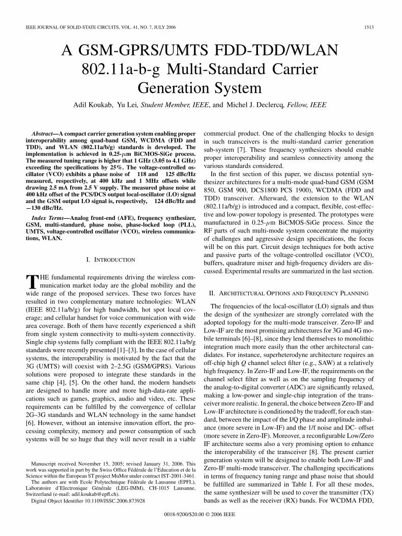
The frequencies of the local-oscillator (LO) signals and thusthe design of the synthesizer are strongly correlated with theadopted topology for the multi-mode transceiver. Zero-IF andLow-IF are the most promising architectures for 3G and 4G mo-bile terminals [6]–[8], since they lend themselves to monolithicintegration much more easily than the other architectural can-didates. For instance, superheterodyne architecture requires anoff-chip high Q channel select filter (e.g., SAW) at a relativelyhigh frequency. In Zero-IF and Low-IF, the requirements on thechannel select filter as well as on the sampling frequency ofthe analog-to-digital converter (ADC) are significantly relaxed,making a low-power and single-chip integration of the trans-ceiver more realistic. In general, the choice between Zero-IF andLow-IF architecture is conditioned by the tradeoff, for each stan-dard, between the impact of the I/Q phase and amplitude imbal-ance (more severe in Low-IF) and the 1/f noise and DC- offset(more severe in Zero-IF). Moreover, a reconfigurable Low/ZeroIF architecture seems also a very promising option to enhancethe interoperability of the transceiver [8]. The present carriergeneration system will be designed to enable both Low-IF andZero-IF multi-mode transceiver. The challenging specificationsin terms of frequency tuning range and phase noise that shouldbe fulfilled are summarized in Table I. For all these modes,the same synthesizer will be used to cover the transmitter (TX)bands as well as the receiver (RX) bands. For WCDMA FDD,
0018-9200/$20.00 © 2006 IEEE
1514 IEEE JOURNAL OF SOLID-STATE CIRCUITS, VOL. 41, NO. 7, JULY 2006
TABLE IBRIEF DESCRIPTION OF THE TARGETED STANDARDS
TABLE IIFREQUENCY PLANNING
where TX and RX are active at the same time, only the TX bandwill be covered by the LO.
Frequency planning and optimization is necessary to enableproper interoperability between such heterogeneous standards.The first obvious optimization constraints are the phase noiseand the tuning range, summarized in Table I. In addition, thecost in terms of power consumption, area, and complexity ofthe final multi-standard system should be optimized to a min-imum level. This objective can be achieved only if the standardsshare a maximum of functionalities and components inside thecarrier generation system. The final constraint that should beintroduced is a precise generation of the quadrature I/Q signalsfor each standard. In fact, since Zero-IF and/or Low-IF archi-tectures are considered as the optimal choices, quadrature pathsare necessary for the complex processing. The quadrature sig-nals can be generated directly by a quadrature VCO (QVCO), bya polyphase filter or by a frequency divider circuit (prescaler).
The prescaler is the most optimal choice for low power andhigh precision, even if this solution requires a higher VCOfrequency (two times the frequency of the I/Q signals). Infact, doubling the VCO frequency is also an advantage since
it helps to avoid frequency pulling and pushing, and decreasethe self-mixing and DC-offset phenomena. In the case of theQVCO solution, the major drawback is the cost in terms ofarea and power consumption. QVCO is constituted by crosscoupling two differential VCOs, thus doubling the requiredarea. Its power dissipation is also, in general, huge compared toa single-stage oscillator. Similar weaknesses characterize thepolyphase filter solution. In fact, since the topology is based onthe classical RC-RC phase-shifter network, the quadrature shiftprecision is strongly dependent on the process variation andmismatches. On the other hand, the order of the polyphase filtershould be increased to broaden the frequency band where thequadrature shift is achieved. Increasing the number of stagesincreases the resistive loss and thus requires more bufferingand more power consumption. For wideband applications,such as 802.11.a where the quadrature generation should beensured over more than 800 MHz, the power consumption ofthe polyphase filters can become prohibitive [9].
From this preliminary analysis, the ideal solution would useonly one wideband VCO and employ frequency dividers tocover the desired standards as well as to generate the precise
KOUKAB et al.: A GSM-GPRS/UMTS FDD-TDD/WLAN 802.11a-b-g MULTI-STANDARD CARRIER GENERATION SYSTEM 1515
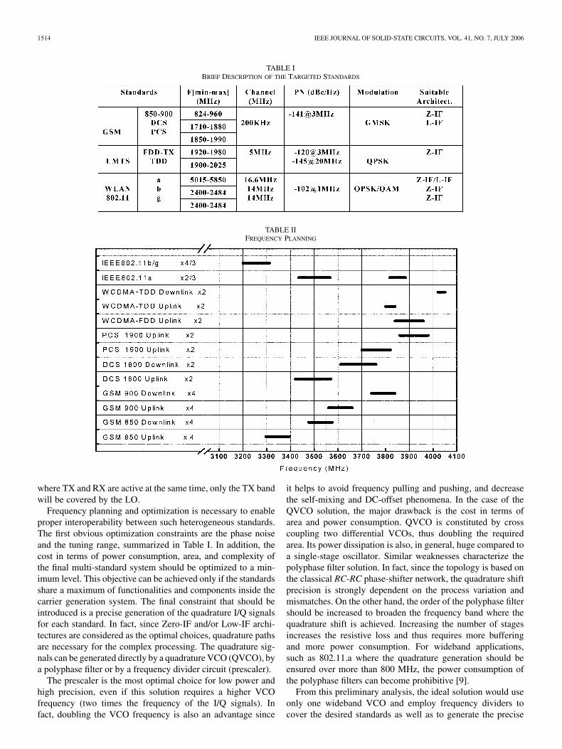
Fig. 1. Multi-mode frequency synthesizer architecture.
quadrature I and Q signals. This approach, however, is onlypossible if we can design a VCO covering a frequency bandfrom 824 MHz 8 (i.e., 6.5 GHz) to 5850 MHz 2 (i.e., 11.7GHz) (see Table I). We should add to this tuning range a marginof at least 10% to cover the process and temperature variation.Moreover, this VCO should fulfill the most challenging phasenoise specification imposed by the GSM standards. Obviously,an on-chip VCO with such tuning range and fulfilling the strin-gent GSM phase noise specifications is practically impossibleto design.
The alternative solution developed to meet these require-ments, without leading to an unrealistic design, is shown inTable II. As illustrated in the table, only a VCO with a frequencytuning of 754 MHz, that is from 3296 MHz (4xGSM850) to4050 MHz (2xWCDMA-TDD downlink), is necessary to coverthe whole of the desired spectrum. This planning has also theadvantage of setting the VCO frequencies out of the bands ofthe standards considered. The silicon implementation of thisfrequency planning results in a compact and cost-effectivecarrier generation system as illustrated in the next section. Itwill enable the generation of a precise quadrature signal for allthe standards at a minimum cost, i.e., using neither QVCO norpolyphase filters.
III. IMPLEMENTATION
A. System Topology
The architecture implementing the frequency plan of Table IIis illustrated in Fig. 1. The interoperability between suchheterogeneous standards will cost only few additional blocks,typically a quadrature balanced mixer and a prescaler forthe 802.11a-b-g. GSM, PCS, DCS, and UMTS frequenciesare generated by two successive divide-by-2 prescalers. The
complexity, cost, and power dissipation will be comparableto a single standard synthesizer. The I and Q signals will begenerated by dividers for all the standards considered.
B. VCO Design
The VCO is the most critical block to design in the synthe-sizer. Several parameters impact the phase noise of the VCO asillustrated by the widely used Leeson formula [10]
(1)
This equation suggests that the phase noise at a frequencyoffset depends on the voltage swing , the oscillation fre-quency , the tank impedance at the resonance , the qualityfactor of the tank , the excess noise factor . is thefrequency of the corner between the and regionsin the noise spectrum. The GSM mode requires a phase noisesignificantly low compared to the other standards. The worstcondition is set by the 23 dBm@3 MHz blocker in e-GSMRX and gives a phase noise limit of 141 dBc/Hz@3 MHz [6].The first intuitive way to achieve this noise level is to increasethe oscillation swing [see (1)] and so to increase the VCOpower consumption. This solution, however, leads to a signifi-cant waste of power when the VCO works for the standards thattolerate a higher noise such as WLAN and UMTS. Therefore,a particular effort should be made to design a reconfigurablemulti-mode VCO with not only a high tuning range but alsogood phase-noise performances and low power dissipation.
The optimization process of the tradeoffs between tuningrange, phase noise, and power consumption has lead to the hy-brid MOS-BJT topology shown in Fig. 2. To form the negativeresistance, the complementary cross-coupled nMOS–pMOS

1516 IEEE JOURNAL OF SOLID-STATE CIRCUITS, VOL. 41, NO. 7, JULY 2006
Fig. 2. VCO and buffers schematic.
structure was preferred to a BJT implementation. In fact, even ifthe BJT has a higher per unit current and lower flicker noisecorner than CMOS transistors, the finite base resistance se-verely limits the maximum attainable oscillation frequency fora given power budget [11]. At high frequency, the impedancecorresponding to the base-emitter capacitance becomescomparable to , decreasing the portion of the base voltagethat will appear across and thus degrading the negativeresistance of the BJT pair.
Another major drawback in BJT-VCOs is the fact that theDC value of their output signal is close to . This specifi-cation limits seriously the tuning range of the VCO. In fact,the middle of the tuning range of practically all the varactors(nMOS, pMOS, or PN diode) is reached when the tuning voltageis close to the VCO DC value by typically 0.5 V. The varac-tors can be AC-coupled to the tank via MIM capacitors and theirgates biased at to avoid this problem. However, the costof this solution in terms of area and parasitic capacitance be-comes prohibitive when a switched-varactors network is usedfor digital tuning.
In the case of the MOS-based VCO, the gate resistance canbe significantly reduced by using a multiple-finger layout, pre-serving a low negative resistance at high frequency. Moreover,in the complementary nMOS–pMOS configuration of Fig. 2, thecurrent is used twice for amplification [12] and the DC value ofthe output signal can easily be tuned to . This structure isthus particularly suitable to achieve low power, low noise, andhigh tuning range design.
The cross coupled pairs of the VCO act as a mixer and down-converts the low-frequency noise and flicker noise of the ac-tive parts near the carrier, leading mainly to AM noise [13].This noise is amplified by the positive feedback, shaped by thetank and finally translated to phase noise by AM–PM conver-sion. The tail current is generally considered as the most sig-nificant source of flicker noise in differential LC VCOs [14].
This is why the low flicker noise BJT was preferred to the noisyMOS transistor in the current-mirror implementation (Fig. 2). Aconfiguration with a 4-bit switched-capacitor network for coarsetuning followed by a small varactor for fine tuning was preferredto a single large varactor. Large varactors are characterized bya steep and nonlinear characteristic and so increase theharmonic distortion of the signal and the AM–PM noise con-version [14]. The gate overdrive as well as the tran-sistor cut-off frequencies was maximized to increase thelinearity of the MOS differential pairs. As illustrated by (2) and(3), the optimal choice to minimize the distortion and so theAM–PM noise conversion will be the lowest transistor widths.At the same time, these widths should be large enough to assurea sufficient margin to ensure the oscillation. The current ispreferably fixed at the edge of the current-limited regime [15] toguarantee a maximum voltage swing without an excessive wasteof power.
(2)
(3)
The buffers used to drive prescaler and to drive output ampli-fiers, package, PCB parasitics, bias tees and spectrum analyzerare shown in Fig. 2. NPN and PNP BJT emitter-follower topolo-gies were used due to their high input impedance and wide band-width. These buffers enable a transfer of the VCO signal to theprescaler without any attenuation.
C. Prescaler and Mixer
The prescaler schematic is illustrated in Fig. 3. A high-speedtopology similar to the standard master/slave ECL D-flip-flopbut without current sources was used. Removing the currentsources increases the maximum toggle frequency and reducespower consumption [16]. However, omitting the current sourceimplies that, in order to drive the input transistors sufficientlyinto and out of saturation, the input signal swing must be largeenough. This condition is satisfied thanks to the buffers (Fig. 2)and the output swing of the VCO which was originally maxi-mized for low phase noise.
To generate the quadrature WLAN carriers, the outputdifferential signals I and Q of the prescaler are mixed withthe VCO outputs using the Gilbert-type circuit (Fig. 4). Thismethod has the advantage of requiring only a quadrature mixerand no QVCO, saving in this way significant area and power.The quadrature mixer is designed to consume only 2x1.4 [email protected] V and the single-stage VCO 2.5 [email protected] V. Obviously, thisadvantage is realized at the cost of a strong sideband at the halfof the VCO frequency that is between 1.5 and 2 GHz. Therefore,an image reject filter in RX and TX paths in conjunction prefer-ably with an LC filter at the WLAN output of the LO will benecessary to overcome image problem and spurious emission.The fact that the spurs are situated far—more than 3 GHz—fromthe desired 5 GHz signals makes the integration of such filtersmuch easier [17], [18].
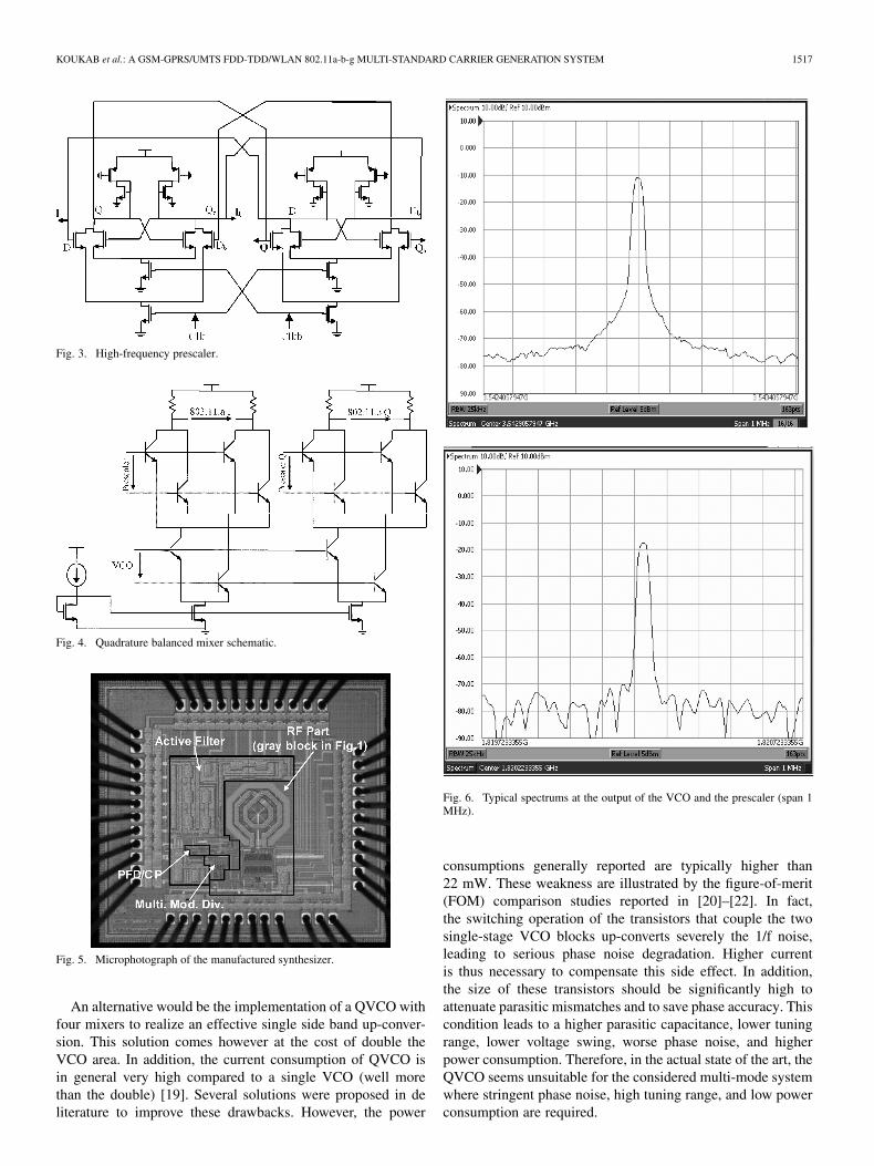
KOUKAB et al.: A GSM-GPRS/UMTS FDD-TDD/WLAN 802.11a-b-g MULTI-STANDARD CARRIER GENERATION SYSTEM 1517
Fig. 3. High-frequency prescaler.
Fig. 4. Quadrature balanced mixer schematic.
Fig. 5. Microphotograph of the manufactured synthesizer.
An alternative would be the implementation of a QVCO withfour mixers to realize an effective single side band up-conver-sion. This solution comes however at the cost of double theVCO area. In addition, the current consumption of QVCO isin general very high compared to a single VCO (well morethan the double) [19]. Several solutions were proposed in deliterature to improve these drawbacks. However, the power
Fig. 6. Typical spectrums at the output of the VCO and the prescaler (span 1MHz).
consumptions generally reported are typically higher than22 mW. These weakness are illustrated by the figure-of-merit(FOM) comparison studies reported in [20]–[22]. In fact,the switching operation of the transistors that couple the twosingle-stage VCO blocks up-converts severely the 1/f noise,leading to serious phase noise degradation. Higher currentis thus necessary to compensate this side effect. In addition,the size of these transistors should be significantly high toattenuate parasitic mismatches and to save phase accuracy. Thiscondition leads to a higher parasitic capacitance, lower tuningrange, lower voltage swing, worse phase noise, and higherpower consumption. Therefore, in the actual state of the art, theQVCO seems unsuitable for the considered multi-mode systemwhere stringent phase noise, high tuning range, and low powerconsumption are required.
1518 IEEE JOURNAL OF SOLID-STATE CIRCUITS, VOL. 41, NO. 7, JULY 2006
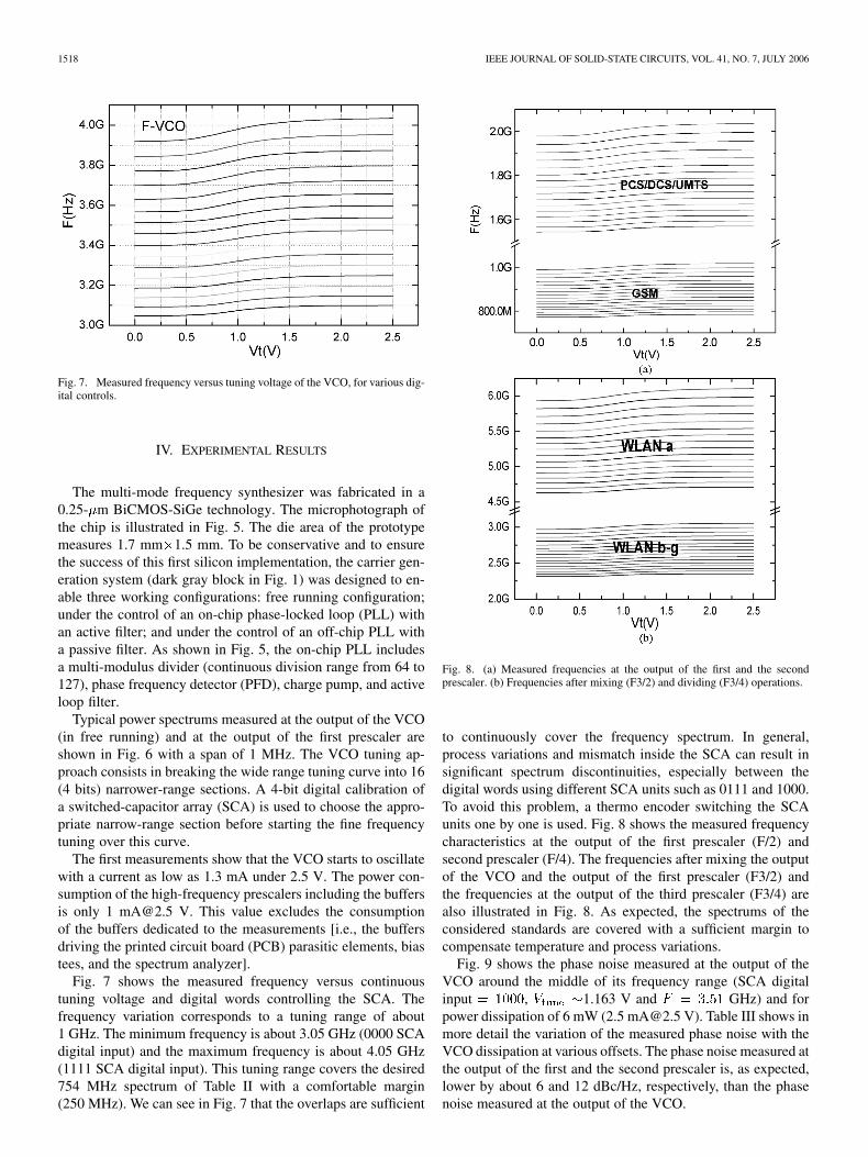
Fig. 7. Measured frequency versus tuning voltage of the VCO, for various dig-ital controls.
IV. EXPERIMENTAL RESULTS
The multi-mode frequency synthesizer was fabricated in a0.25- m BiCMOS-SiGe technology. The microphotograph ofthe chip is illustrated in Fig. 5. The die area of the prototypemeasures 1.7 mm 1.5 mm. To be conservative and to ensurethe success of this first silicon implementation, the carrier gen-eration system (dark gray block in Fig. 1) was designed to en-able three working configurations: free running configuration;under the control of an on-chip phase-locked loop (PLL) withan active filter; and under the control of an off-chip PLL witha passive filter. As shown in Fig. 5, the on-chip PLL includesa multi-modulus divider (continuous division range from 64 to127), phase frequency detector (PFD), charge pump, and activeloop filter.
Typical power spectrums measured at the output of the VCO(in free running) and at the output of the first prescaler areshown in Fig. 6 with a span of 1 MHz. The VCO tuning ap-proach consists in breaking the wide range tuning curve into 16(4 bits) narrower-range sections. A 4-bit digital calibration ofa switched-capacitor array (SCA) is used to choose the appro-priate narrow-range section before starting the fine frequencytuning over this curve.
The first measurements show that the VCO starts to oscillatewith a current as low as 1.3 mA under 2.5 V. The power con-sumption of the high-frequency prescalers including the buffersis only 1 [email protected] V. This value excludes the consumptionof the buffers dedicated to the measurements [i.e., the buffersdriving the printed circuit board (PCB) parasitic elements, biastees, and the spectrum analyzer].
Fig. 7 shows the measured frequency versus continuoustuning voltage and digital words controlling the SCA. Thefrequency variation corresponds to a tuning range of about1 GHz. The minimum frequency is about 3.05 GHz (0000 SCAdigital input) and the maximum frequency is about 4.05 GHz(1111 SCA digital input). This tuning range covers the desired754 MHz spectrum of Table II with a comfortable margin(250 MHz). We can see in Fig. 7 that the overlaps are sufficient
Fig. 8. (a) Measured frequencies at the output of the first and the secondprescaler. (b) Frequencies after mixing (F3/2) and dividing (F3/4) operations.
to continuously cover the frequency spectrum. In general,process variations and mismatch inside the SCA can result insignificant spectrum discontinuities, especially between thedigital words using different SCA units such as 0111 and 1000.To avoid this problem, a thermo encoder switching the SCAunits one by one is used. Fig. 8 shows the measured frequencycharacteristics at the output of the first prescaler (F/2) andsecond prescaler (F/4). The frequencies after mixing the outputof the VCO and the output of the first prescaler (F3/2) andthe frequencies at the output of the third prescaler (F3/4) arealso illustrated in Fig. 8. As expected, the spectrums of theconsidered standards are covered with a sufficient margin tocompensate temperature and process variations.
Fig. 9 shows the phase noise measured at the output of theVCO around the middle of its frequency range (SCA digitalinput , 1.163 V and GHz) and forpower dissipation of 6 mW (2.5 [email protected] V). Table III shows inmore detail the variation of the measured phase noise with theVCO dissipation at various offsets. The phase noise measured atthe output of the first and the second prescaler is, as expected,lower by about 6 and 12 dBc/Hz, respectively, than the phasenoise measured at the output of the VCO.

KOUKAB et al.: A GSM-GPRS/UMTS FDD-TDD/WLAN 802.11a-b-g MULTI-STANDARD CARRIER GENERATION SYSTEM 1519
Fig. 9. VCO phase noise with V = 1:163 V and digital control = 1000.
TABLE IIIMEASURED PHASE NOISE VERSUS VCO CONSUMPTION
TABLE IVCOMPARISON OF THE NORMALIZED FOM
Table IV shows a comparative study between the designedVCO and the recently published ones by using the widely usednormalized FOM [29]:
FOM MHz mW
dBc/Hz/mW. (4)
The calculated FOM for our VCO from the measured data is189.25 dBc/Hz/mW. Among the circuits that have been com-
pared, this VCO exhibits one of the best FOMs, confirming the
Fig. 10. Typical settling time and spectrum of the synthesizer.
excellent phase noise/power consumption tradeoffs achieved.Moreover, this figure is realized without sacrificing the tuningrange (around 30% of the center frequency).
An additional set of measurements of the carrier generationsystem under a PLL control were achieved. The prototype withthe off-chip PLL enables the optimization of the passive filter;its performances are thus higher compared to the fully inte-grated version. Fig. 10 illustrates a typical measured settlingtime during the fine tuning with an SCA digital word of 1101.The bandwidth of the PLL is 20 kHz, the reference frequencyis supplied by a 16.38 MHz crystal oscillator, and the passivefilter is a second-order type with , nF, and
nF. In this configuration, the PLL is locked from 3.84to 3.778 GHz within 1 kHz tolerance in 80 s. Fig. 10 shows alsothe measured spectrum of the PLL after locking (span 15 MHz).The measured phase noise of the frequency synthesizer after thefine tuning is illustrated in Fig. 11.

1520 IEEE JOURNAL OF SOLID-STATE CIRCUITS, VOL. 41, NO. 7, JULY 2006
Fig. 11. Phase noise of the VCO in free running and under the PLL control.
V. CONCLUSION
A compact and cost-effective frequency synthesizer architec-ture enabling the convergence of such heterogeneous standardsas quad-band GSM (GSM 850, GSM 900, DCS1800 PCS1900), WCDMA (FDD and TDD), and WLAN (802.11a/b/g)in the same terminal has been developed. The design andmanufacturing has been achieved with 0.25- m BiCMOS SiGeprocess. The experimental results show that the tuning range isabout 1 GHz (3.05–4.05 GHz) exceeding the specification by25% (Table I). A hybrid nMOS–pMOS–Bipolar VCO topologyrepresenting an optimal tradeoff between phase noise, powerconsumption, tuning range, and sensitivity to noise has beenpresented. This VCO exhibits a phase noise of 125 dBc/Hzmeasured at 1 MHz offset while drawing only 2.5 mA from2.5 V supply. The measured phase noise at 400 kHz offsetof the PCS/DCS signal (output of the first prescaler) and theGSM signal (output the second prescaler) is, respectively,
124 dBc/Hz and 130 dBc/Hz. The circuit exhibits anFOM of 189.25 dBc/Hz/mW, confirming the excellent phasenoise/power consumption tradeoffs achieved.
REFERENCES
[1] Z. Xu et al., “A compact dual-band direct-conversion CMOS trans-ceiver for 802.11a/b/g WLANs,” in IEEE ISSCC Dig. Tech. Papers,Feb. 2005, pp. 98–99.
[2] P. Zhan et al., “A single-chip dual-band direct-conversion IEEE 802.11a/b/g WLAN transceiver in 0.18-�m CMOS,” IEEE J. Solid-State Cir-cuits, vol. 40, no. 9, pp. 1932–1939, Sep. 2005.
[3] M. Zannoth, T. Rühlicke, and B.-U. Klepser, “A highly integrated dual-band multimode wireless LAN transceiver,” IEEE J. Solid-State Cir-cuits, vol. 39, no. 7, pp. 1191–1195, Jul. 2004.
[4] H.-I. Lee et al., “A �-� fractional-N frequency synthesizer using awideband integrated VCO and a fast AFC technique for GSM/GPRS/WCDMA application,” IEEE J. Solid-State Circuits, vol. 39, no. 7, pp.1164–1169, Jul. 2004.
[5] J. Ryynanen et al., “A single-chip multi-mode receiver for GSM900DCS1800, PCS1900, and WCDMA,” IEEE J. Solid-State Circuits, vol.38, no. 4, pp. 594–602, Apr. 2004.
[6] M. Brandolini, P. Rossi, D. Manstretta, and F. Svelto, “Toward multi-standard mobile terminals—fully integrated receiver requirements andarchitectures,” IEEE Trans. Microw. Theory Tech., vol. 53, no. 3, pp.1026–1038, Mar. 2005.
[7] A. Koukab, Y. Lei, and M. Declercq, “Multi-standard carrier gen-eration system for quad-band GSM/WCDMA (FDD-TDD)/WLAN(802.11 a-b-g) radio,” in Proc. ESSCIRC, Sep. 2005, pp. 177–180.
[8] S. L. J. Gierkink, D. Li, R. C. Frey, and V. Boccuzzi, “A 3.5-GHz PLLfor fast Low-IF/Zero-IF LO switching in an 802.11 transceiver,” IEEEJ. Solid-State Circuits, vol. 38, no. 9, pp. 1909–1921, Sep. 2005.
[9] D. I. Sanderson, R. M. Svitek, and S. Raman, “ A 5-6-GHz polyphasefilter with tunable I/Q phase balance,” IEEE Microw. Wireless Compon.Lett., vol. 14, no. 7, pp. 364–366, Jul. 2004.
[10] D. Leeson, “A simple model of feedback oscillator noise spectrum,”Proc. IEEE, vol. 54, no. 2, pp. 329–330, Feb. 1966.
[11] B. Jung and R. Harjani, “High-frequency LC VCO design using capac-itive degeneration,” IEEE J. Solid-State Circuits, vol. 39, no. 12, pp.2359–2369, Dec. 2004.
[12] A. Hajimiri and T. H. Lee, “A general theory of phase noise in electricaloscillators,” IEEE J. Solid-State Circuits, vol. 33, no. 2, pp. 179–194,Feb. 1998.
[13] A. Jerng and C. G. Sodini, “The impact of devices type and sizing onphase noise mechanisms,” IEEE J. Solid-State Circuits, vol. 40, no. 2,pp. 360–369, Feb. 2005.
[14] S. Lavantino, C. Samori, A. Bonfanti, S. L. J. Gierkink, A. L. Laciata,and V. Boccuzzi, “Frequency dependence on bias current in 5-GHzCMOS VCO: impact on tuning range and flicker noise upconversion,”IEEE J. Solid-State Circuits, vol. 37, no. 8, pp. 1003–1011, Aug. 2002.
[15] D. Ham and A. Hajimiri, “Concepts and methods in optimization ofintegrated LC VCOs,” IEEE J. Solid-State Circuits, vol. 36, no. 6, pp.896–909, Jun. 2001.
[16] J. Craninckx and M. Steyaert, “A 1.8-GHz low-phase-noise voltagecontrolled oscillator with prescaler,” IEEE J. Solid-State Circuits, vol.30, no. 12, pp. 1474–1482, Dec. 1995.
[17] H. Darabi et al., “A 2.4-GHz CMOS transceiver for Bluetooth,” IEEEJ. Solid-State Circuits, vol. 36, no. 12, pp. 2016–2024, Dec. 2001.
[18] H. Shin, Z. Xu, and M. F. Chang, “A 1.8-V 6/9-GHz reconfigurabledual-band quadrature LC VCO in SiGe BiCMOS technology,” IEEE J.Solid-State Circuits, vol. 38, no. 6, pp. 1028–1032, Jun. 2003.
[19] A. Chung and J. R. Long, “A 5–6 bipolar quadrature-phase generator,”IEEE J. Solid-State Circuits, vol. 39, no. 10, pp. 1737–1745, Oct. 2004.
[20] M. Tiebout, “Low-power low-phase-noise differentially tuned quadra-ture VCO design in standard CMOS,” IEEE J. Solid-State Circuits, vol.36, no. 7, pp. 1018–1024, Jul. 2001.
[21] S. L. J. Gierkink et al., “A low-phase noise 5-GHz CMOS quadratureVCO using superharmonic coupling,” IEEE J. Solid-State Circuits, vol.38, no. 7, pp. 1148–1154, Jul. 2003.
[22] H.-R. Kim, C.-Y. Cha, S.-M. Oh, M.-S. Yang, and S.-G. Lee, “A verylow-power VCO with back-gate coupling,” IEEE J. Solid-State Cir-cuits, vol. 39, no. 6, pp. 952–955, Jun. 2004.
[23] M. A. Margarit, D. Shih, P. J. Sullivan, and F. Ortega, “A 5-GHzBiCMOS RFIC front-end for IEEE 802.11a/HiperLAN wirelessLAN,” IEEE J. Solid-State Circuits, vol. 38, no. 7, pp. 1284–1287,Jul. 2003.
[24] J. Rogers and C. Plett, “A 5-GHz radio front-end with automaticallyQ-tuned notch filter and VCO,” IEEE J. Solid-State Circuits, vol. 38,no. 9, pp. 1547–1554, Sep. 2003.
[25] N. Fong, J. Plouchart, N. Zamdmer, D. Liu, L. Wagner, C. Plett, andN. Tarr, “Design of wideband CMOS VCO for multiband wirelessLAN applications,” IEEE J. Solid-State Circuits, vol. 38, no. 8, pp.1333–1342, Aug. 2003.
[26] Y. K. Chu and H. R. Chuang, “A fully integrated 5.8 GHz U-NII band0.18-�m CMOS VCO,” IEEE Microw. Wireless Compon. Lett., vol. 13,no. 7, pp. 287–289, Jul. 2003.
[27] Y. Eo, K. Kim, and B. Oh, “Low noise 5 GHz differential VCO usingInGaP/GaAs HBT technology,” IEEE Microw. Wireless Compon. Lett.,vol. 13, no. 7, pp. 259–261, Jul. 2003.
[28] M.-D. Tsai, Y.-H. Cho, and H. Wang, “A 5-GHz low phase noise dif-ferential Colpitts CMOS VCO,” IEEE Microw. Wireless Compon. Lett.,vol. 15, no. 5, pp. 327–329, May 2005.
[29] P. Kinget, “Integrated GHz voltage controlled oscillators,” in AnalogCircuit Design: (X)DSL and Other Communication Systems; RF MOSTModels; Integrated Filters and Oscillators, W. Sansen, J. Huijsing, andR. van de Plassche, Eds. Boston, MA: Kluwer, 1999, pp. 353–381.
KOUKAB et al.: A GSM-GPRS/UMTS FDD-TDD/WLAN 802.11a-b-g MULTI-STANDARD CARRIER GENERATION SYSTEM 1521
Adil Koukab received the M.S. degree (DEAd’Opto-Electronique) from the University of Nancy,France, in 1993 and the Ph.D. degree in electricalengineering from the University of Metz andSupélec, France, in 1997. His research work wason the physics, modeling and characterization ofmicroelectronic devices based on III-V compoundsemiconductor materials (especially InP and relatedmaterials) and of deep-submicron MOSFETs.
He is currently a Research Associate with the De-partment of Electrical Engineering of the Swiss Fed-
eral Institute of Technology (EPFL), Lausanne, Switzerland. His present re-search interests include design, design methodology and EDA development forRF, analog, and mixed-signal ICs, and physical parasitic effects, cross-talk andsubstrate noise in MS-SOC designs.
Yu Lei (S’03) received the B.S. degree from Xi’DianUniversity, China, in 1997 and the M.S. degree fromShanghai Jiaotong University in 2000.
He was with Trident Micro Inc. from 2000 to 2003as a Research Engineer. In 2003, he joined LEG,EPFL, Lausanne, Switzerland. His current researchinterests include high-speed and low-power analogIC design and RF IC design.
Michel J. Declercq (S’70–M’72–SM’93–F’00)received the Electrical Engineering degree andthe Ph.D. degree from the Catholic University ofLouvain, Belgium, in 1967 and 1971, respectively.
In 1973, he was awarded a Senior Fulbright Fel-lowship, and joined Stanford University, Stanford,CA, as a Research Associate in the MicroelectronicsLabs. From 1974 to 1978, he was Research Associateand lecturer at the Catholic University of Louvain. In1978, he joined Tractebel, Brussels, Belgium, wherehe was Group Leader of the Electronic Systems
team. In 1985, he joined the Swiss Federal Institute of Technology (EPFL),Lausanne, Switzerland, where he is currently Professor, Dean of the School ofEngineering, and Director of the Electronics Laboratory. His research activitiesare related to mixed analog-digital IC design and design methodologies. Heis particularly involved in low-power/low-voltage circuits, high-frequencycircuits for telecommunications, MEMS and RF-MEMS, SOI technology andcircuits, high-voltage circuits and nano-electronics. He is author or coauthor ofmore than 200 scientific publications and two books, and holds several patents.
Prof. Declercq is expert by the European Commission for the scientific re-search programs in information technologies.