Embed Size (px)
Citation preview
IEEE JOURNAL OF SOLID-STATE CIRCUITS, VOL. 44, NO. 1, JANUARY 2009 73
A Sub-2 W Low Power IA Processor for MobileInternet Devices in 45 nm High-k Metal Gate CMOS
Gianfranco Gerosa, Member, IEEE, Steve Curtis, Michael D’Addeo, Bo Jiang, Belliappa Kuttanna,Feroze Merchant, Binta Patel, Mohammed H. Taufique, and Haytham Samarchi
Abstract—This paper describes a low power Intel Architecture(IA) processor specifically designed for Mobile Internet Devices(MID) with performance similar to mainstream Ultra-MobilePCs. The design relies on high residency in a new low-power statein order to keep average power and idle power below 220 and80 mW, respectively. The design consists of an in-order pipelinecapable of issuing 2 instructions per cycle supporting 2 threads,32 KB instruction and 24 KB data L1 caches, independent integerand floating point execution units, x86 front end execution unit, a512 KB L2 cache and a 533 MT/s dual-mode (GTL and CMOS)front-side-bus (FSB). The design contains 47 million transistors ina die size under 25 mm manufactured in a 9-metal 45 nm CMOSprocess with optimized transistors for low leakage. Maximumthermal design power (TDP) consumption is measured at 2 W at1.0 V, 90 C using a synthetic power-virus test at a frequency of1.86 GHz.
Index Terms—Low power Intel Architecture processor, mobileinternet devices.
I. INTRODUCTION
T HIS paper describes a low power Intel Architecture (IA)processor specifically designed for Mobile Internet De-
vices (MID) with performance targeted to mainstream Ultra-Mobile PCs [1]. The design relies on high residency (over 80%)in a new low-power state in order to keep average power andidle power below a few hundred mW. The micro-Architectureis kept simple and only those features that give the best per-formance/watt are incorporated. The resulting processor designconsists of an in-order pipeline capable of issuing 2 instruc-tions per cycle supporting two threads, 32 KB instruction and24 KB data L1 caches, independent integer and floating pointexecution units, x86 front end execution unit, a 512 KB L2cache and a 533 MT/s dual-mode (GTL and CMOS) Front-Side-Bus (FSB). The addition of simultaneous multi-threadingprovide over a 36% increase in performance for a modest 19%increase in power. The design contains 47 M transistors in a diesize under 25 mm manufactured in a 9-metal 45 nm CMOSprocess with optimized transistors for low leakage packagedin a Halide-Free 441 ball, 14 13 mm FCBGA. Maximumthermal design power (TDP) consumption is measured at 2 Wusing a synthetic power-virus test at a frequency of 1.86 GHz. A0.65 W TDP at 800 MHz is achieved at the lowest power supply
Manuscript received April 15, 2008; revised August 31, 2008. Current versionpublished December 24, 2008.
The authors are with Intel Corporation, Austin, TX 78746 USA (e-mail: [email protected]).
Digital Object Identifier 10.1109/JSSC.2008.2007170
Vmin 0.75 volts set by the L2 cache 6-transistor bitcellunder normal operating conditions; retention voltages are lower.Measured average and idle power are in the order of 220 mWand under 80 mW, respectively.
This paper is organized as follows: in Section II, the pro-cessor’s micro-architectural details are presented, Section IIIprovides a glimpse into the 45 nm CMOS technology,Section IV briefly describes the design methodology usedto build this processor, Section V discusses the clock architec-ture, Section VI describes several low power circuit techniquesused, Section VII briefly describes the L2 cache, Section VIIIintroduces two aspects of reducing FSB power, Section IXcovers measured performance and power results and finally, inSection X, we conclude the paper.
II. MICRO-ARCHITECTURE
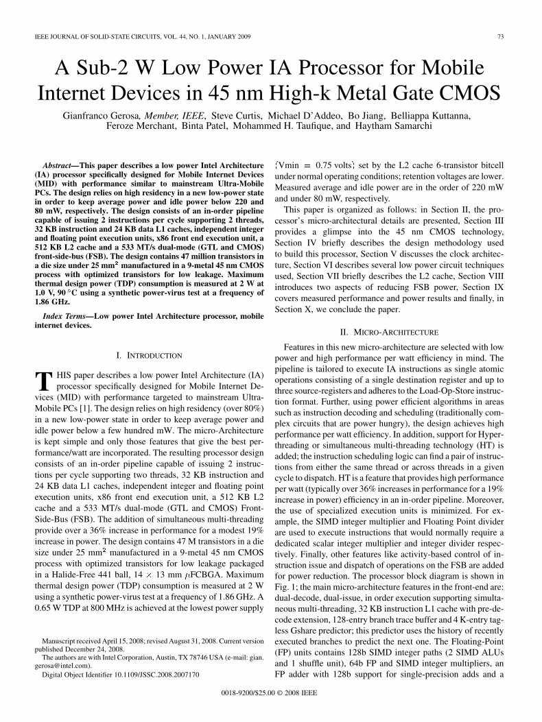
Features in this new micro-architecture are selected with lowpower and high performance per watt efficiency in mind. Thepipeline is tailored to execute IA instructions as single atomicoperations consisting of a single destination register and up tothree source-registers and adheres to the Load-Op-Store instruc-tion format. Further, using power efficient algorithms in areassuch as instruction decoding and scheduling (traditionally com-plex circuits that are power hungry), the design achieves highperformance per watt efficiency. In addition, support for Hyper-threading or simultaneous multi-threading technology (HT) isadded; the instruction scheduling logic can find a pair of instruc-tions from either the same thread or across threads in a givencycle to dispatch. HT is a feature that provides high performanceper watt (typically over 36% increases in performance for a 19%increase in power) efficiency in an in-order pipeline. Moreover,the use of specialized execution units is minimized. For ex-ample, the SIMD integer multiplier and Floating Point dividerare used to execute instructions that would normally require adedicated scalar integer multiplier and integer divider respec-tively. Finally, other features like activity-based control of in-struction issue and dispatch of operations on the FSB are addedfor power reduction. The processor block diagram is shown inFig. 1; the main micro-architecture features in the front-end are:dual-decode, dual-issue, in order execution supporting simulta-neous multi-threading, 32 KB instruction L1 cache with pre-de-code extension, 128-entry branch trace buffer and 4 K-entry tag-less Gshare predictor; this predictor uses the history of recentlyexecuted branches to predict the next one. The Floating-Point(FP) units contains 128b SIMD integer paths (2 SIMD ALUsand 1 shuffle unit), 64b FP and SIMD integer multipliers, anFP adder with 128b support for single-precision adds and a
0018-9200/$25.00 © 2008 IEEE
74 IEEE JOURNAL OF SOLID-STATE CIRCUITS, VOL. 44, NO. 1, JANUARY 2009
Fig. 1. Low power IA processor architecture block diagram.
Safe Instruction Recognition support to allow out-of-order com-mits. The integer execution cluster contains two ALUs, a shifterand a Jump Execution unit; single cycle 64b integer operationsare supported. The memory execution unit contains a 24 KBwrite-back L1 cache with 2-level data TLB hierarchy, hard-ware page walker, integer store to load forwarding support, a512 KB L2 cache with inline ECC and L2/data cache hardwarepre-fetchers. Other micro-architecture features include Intel 64Architecture support, Intel Digital Media Boost (SSE3), andIntel Virtualization technology. A detailed look at the micro-ar-chitecture can be found in [5] and [6].
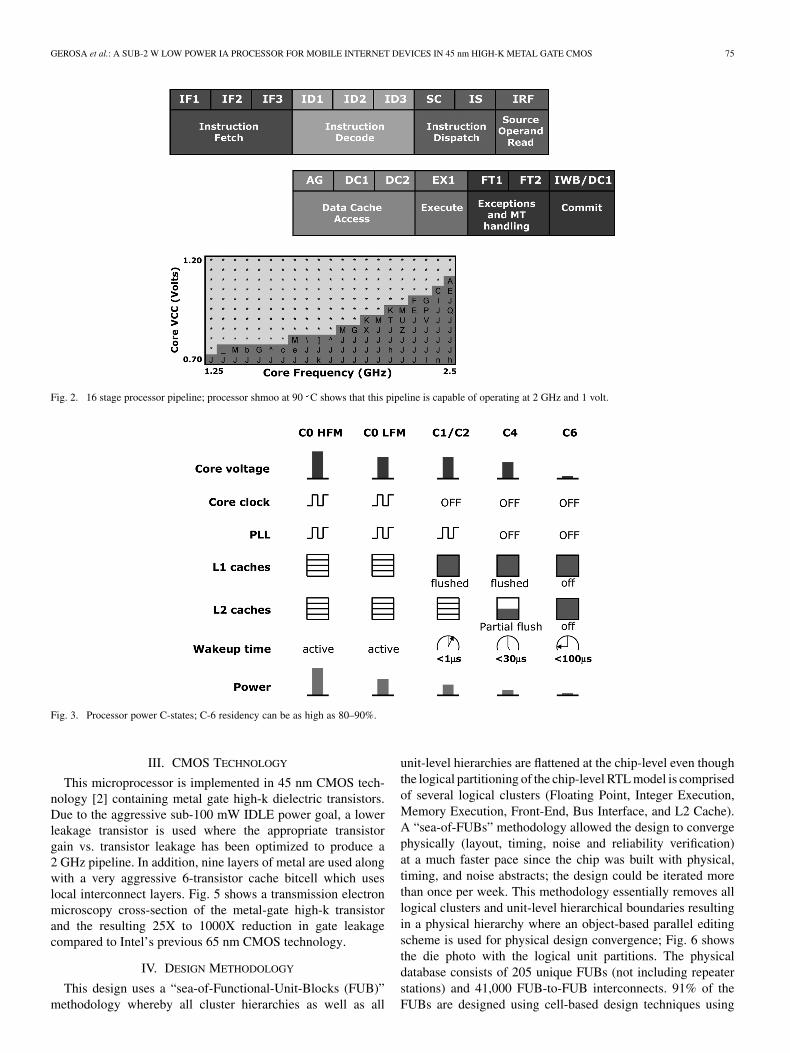
Fig. 2 shows the 16-stage pipeline starting with instructionfetch of an integer macro-instruction through when the resultsare either committed to the register file or the data cache. Theincluded processor shmoo (thousands of functional patterns areused) clearly show that a 2 GHz core frequency at 1 V is clearlyachievable. Also note that lower frequencies (down to 600 MHz)are possible at a power supply of 0.75 V by simply dialing downthe core phase-lock loop (PLL) ratio.
Several features support extended battery life including thenew Intel Deep Power Down Technology [3] which allows fora majority of the CPU functionality to be powered down ex-
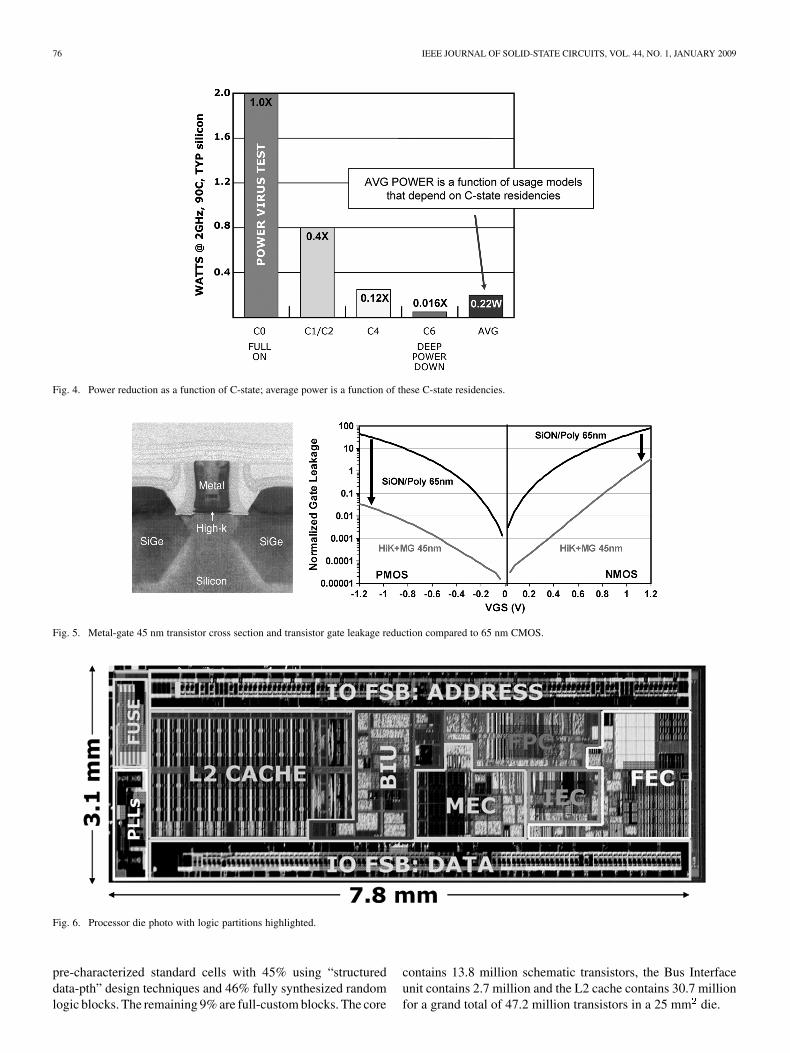
cept for an on-die array that holds the micro-architectural statewith very fast entry/exit times 100 s . Fig. 3 shows severalpower states (C-states) where lower power is achieved as morefeatures are turned off from C-0 state to C-6 state. In C-0 highfrequency mode (HFM) and low frequency mode (LFM), theprocessor can operate at its maximum frequency and its min-imum frequency, respectively. In C-1 power state the core clockis power-gated and the L1 caches flushed resulting in lower dy-namic power; exit latency is under 1 s. In C-4 power state,the 2 PLLs are shut down, the L1 caches are flushed leading tofurther dynamic power reduction; exit latencies are in the orderof 30 s. Finally, in C-6 power state, the state of the machineis stored in an on-die SRAM (built as a 1-read, 1-write portedregister file) and the core power supply is shut down resultingin the lowest power; exit latencies are in the order of 100 s.Fig. 4 shows the power savings among all these C-states; theAVERAGE power is clearly a function of the processor’s res-idency in these C-states; based on preliminary measurements,we estimate C-6 residency to be between 80% and 90% leadingto an AVERAGE power in the order of 220 mW. IDLE powerwhich is dominated by leakage power of the remaining poweredfunctional units on die is below 80 mW.
GEROSA et al.: A SUB-2 W LOW POWER IA PROCESSOR FOR MOBILE INTERNET DEVICES IN 45 nm HIGH-K METAL GATE CMOS 75
Fig. 2. 16 stage processor pipeline; processor shmoo at 90 C shows that this pipeline is capable of operating at 2 GHz and 1 volt.
Fig. 3. Processor power C-states; C-6 residency can be as high as 80–90%.
III. CMOS TECHNOLOGY
This microprocessor is implemented in 45 nm CMOS tech-nology [2] containing metal gate high-k dielectric transistors.Due to the aggressive sub-100 mW IDLE power goal, a lowerleakage transistor is used where the appropriate transistorgain vs. transistor leakage has been optimized to produce a2 GHz pipeline. In addition, nine layers of metal are used alongwith a very aggressive 6-transistor cache bitcell which useslocal interconnect layers. Fig. 5 shows a transmission electronmicroscopy cross-section of the metal-gate high-k transistorand the resulting 25X to 1000X reduction in gate leakagecompared to Intel’s previous 65 nm CMOS technology.
IV. DESIGN METHODOLOGY
This design uses a “sea-of-Functional-Unit-Blocks (FUB)”methodology whereby all cluster hierarchies as well as all
unit-level hierarchies are flattened at the chip-level even thoughthe logical partitioning of the chip-level RTL model is comprisedof several logical clusters (Floating Point, Integer Execution,Memory Execution, Front-End, Bus Interface, and L2 Cache).A “sea-of-FUBs” methodology allowed the design to convergephysically (layout, timing, noise and reliability verification)at a much faster pace since the chip was built with physical,timing, and noise abstracts; the design could be iterated morethan once per week. This methodology essentially removes alllogical clusters and unit-level hierarchical boundaries resultingin a physical hierarchy where an object-based parallel editingscheme is used for physical design convergence; Fig. 6 showsthe die photo with the logical unit partitions. The physicaldatabase consists of 205 unique FUBs (not including repeaterstations) and 41,000 FUB-to-FUB interconnects. 91% of theFUBs are designed using cell-based design techniques using
76 IEEE JOURNAL OF SOLID-STATE CIRCUITS, VOL. 44, NO. 1, JANUARY 2009
Fig. 4. Power reduction as a function of C-state; average power is a function of these C-state residencies.
Fig. 5. Metal-gate 45 nm transistor cross section and transistor gate leakage reduction compared to 65 nm CMOS.
Fig. 6. Processor die photo with logic partitions highlighted.
pre-characterized standard cells with 45% using “structureddata-pth” design techniques and 46% fully synthesized randomlogic blocks. The remaining 9% are full-custom blocks. The core
contains 13.8 million schematic transistors, the Bus Interfaceunit contains 2.7 million and the L2 cache contains 30.7 millionfor a grand total of 47.2 million transistors in a 25 mm die.
GEROSA et al.: A SUB-2 W LOW POWER IA PROCESSOR FOR MOBILE INTERNET DEVICES IN 45 nm HIGH-K METAL GATE CMOS 77
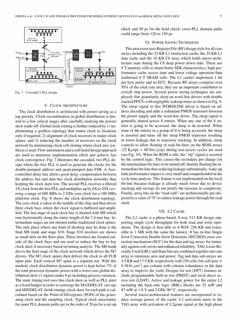
Fig. 7. Cascaded 2 PLL design.
V. CLOCK ARCHITECTURE
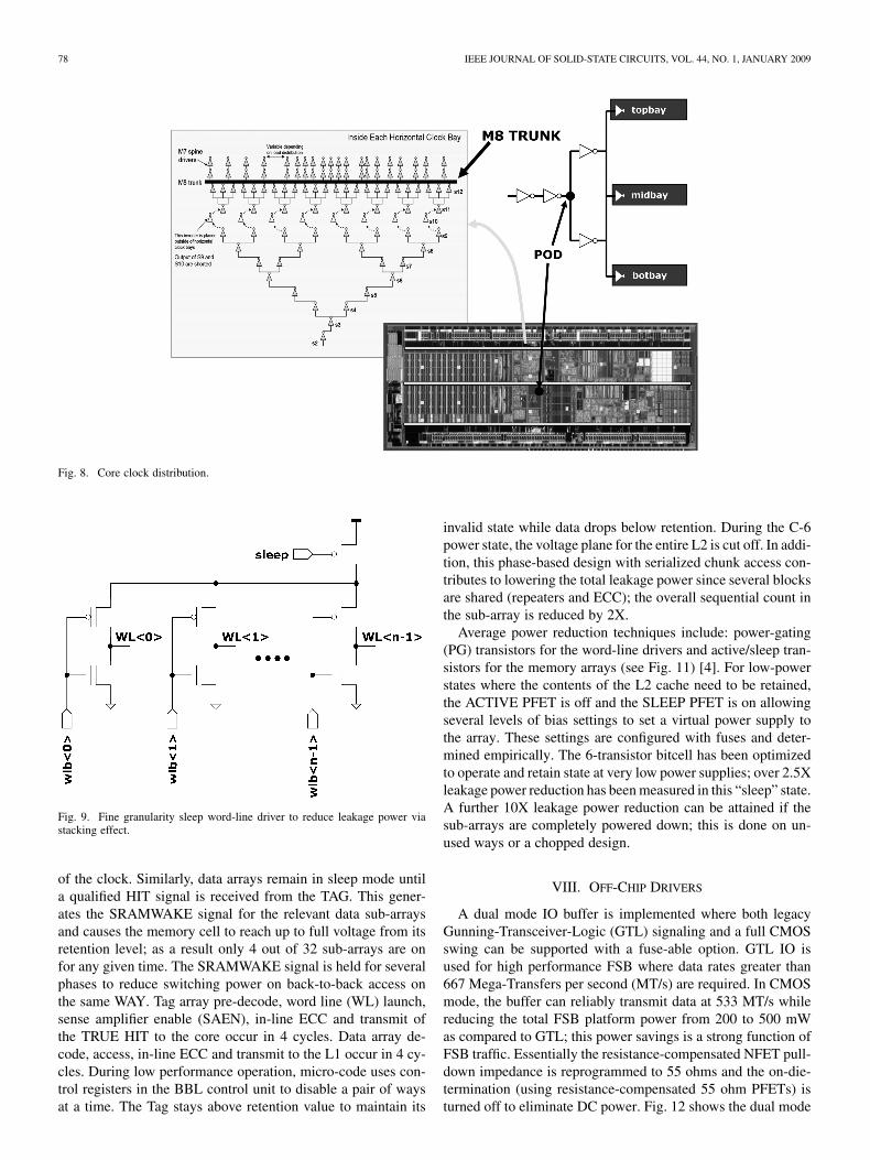
The clock distribution is architected with power saving as atop priority. Clock recombination in global distribution is lim-ited to a few critical stages after carefully studying the power/skew trade-off. Global clock routing is further reduced by 1) im-plementing a gridless topology that routes clock to locationsonly if required, 2) alignment of clock receivers to major clockspines, and 3) reducing the number of receivers on the clocknetwork by minimizing clock cell cloning where clock tree syn-thesis is used. Flow automation and a cell based design approachare used to minimize implementation effort and achieve fastclock convergence. Fig. 7 illustrates the cascaded, two PLL de-sign where the first PLL is used to generate the clocks for thedouble-pumped address and quad-pumped data FSB. A fuse-controlled delay line allows good delay compensation betweenthe address bus and data bus clock distribution networks thuskeeping the clock skew low. The second PLL receives a filtered1X clock from the first PLL and multiplies up by 6X to 20X cov-ering a range of 600 MHz to 2 GHz core clock for a 100 MHzplatform clock. Fig. 8 shows the clock distribution topology.The core clock is taken to the middle of the chip and then drivesthree clock bays where the clock signal is buffered and ampli-fied. The last stage of each clock bay is shorted with M8 whichruns horizontally along the entire length of the 7.4 mm bay. In-termediate stages are not shorted unlike traditional clock spines.The only place where any kind of shorting may be done is thefinal M8 trunk and stage S10. Stage S10 inverters are shownas small dots on the floor plan. These inverters are located out-side of the clock bays and are used to reduce the bay to bayclock skew if necessary based on timing analysis. The M8 trunkdrives the final stage of the clock network which drives the M7drivers. The M7 clock spines then deliver the clock to all FUBinput pins. Each vertical M7 spine is a separate net. With thismethod, clock distribution dynamic power is kept below 7% ofthe total processor dynamic power with a worst case global dis-tribution skew (1 sigma) under 6 ps including process variation.The static timing tool uses this clock skew as well as PLL jitteras a fixed budget in order to converge the MAXDELAY (set-up)and MINDELAY (hold) timing; clock skew for each path is cal-culated based on the Point-of-Divergence (POD) of the gener-ating clock and the sampling clock. Typical clock uncertaintyfor same PLL domain paths are in the order of 20 ps for a set-up
check and 50 ps for the hold check; cross-PLL domain pathscould range from 120 to 150 ps.
VI. POWER SAVING TECHNIQUES
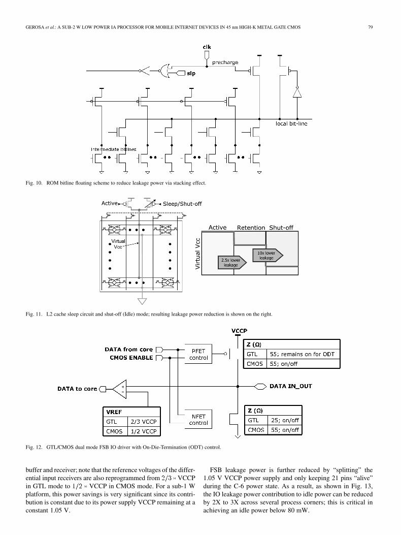
This processor uses Register File (RF) design style for all corearrays including the 32 KB L1 instruction cache, the 24 KB L1data cache and the 10 KB C6 array which holds micro-archi-tecture state during the C6 deep power down state. These use8 T memory cells to attain better SER characteristics, high per-formance cache access time and lower voltage operation thantraditional 6 T SRAM cells. The L1 caches implement 1 bitper byte parity and no ECC. Because RF arrays comprise over50% of the total core area, they are an important contributor tooverall chip power. Several power saving techniques are em-ployed: fine granularity sleep on word-line drivers with doublestacked PFETs with negligible wakeup times as shown in Fig. 9.The sleep signal in this WORDLINE driver is based on ad-dress decoding and adds a redundant PMOS transistor betweenthe power supply and the word-line driver. The sleep signal isgenerally shared across 8 entries. When any one of the 8 en-tries is going to be accessed, the sleep is de-asserted. Whennone of the entries in a group-of-8 is being accessed, the sleepis asserted and turns off the sleep PMOS transistor resultingin lower leakage due to transistor stacking. In addition, sleepcontrols to allow floating of read bit-lines on the ROM arrays22 K ops 60 bits op during non-access cycles are used
(see Fig. 10). When the ROM is idle, the “slp” signal is assertedby the control logic. This causes the secondary pre-charge (onthe intermediate bit-line) to be turned off, thereby floating the in-termediate bit-line thus reducing leakage substantially; wake-uptime performance impact is very small and comprehended in thecycle time analysis. This feature is not implemented on the localbit-line because leakage is already much lower due to devicestacking and savings do not justify the increase in complexity.Finally, array bits on the “read-side” are architecturally pre-dis-posed to a value of “0” to reduce leakage power through the readstack.
VII. L2 CACHE
The L2 cache is a phase-based, 8-way 512 KB design sup-porting single cycle throughput for both read and write oper-ations. The design is fuse-able to 4-WAY 256 KB and exten-sible to 1 MB with the same the latency. It has in-line SingleError Correction Double Error Detection (SECDED) error cor-rection mechanism (ECC) for the data and tag arrays for immu-nity against soft-errors and enhanced reliability. TAG, Least-Re-cently Used (LRU) and State bits are combined together into onearray to minimize area and power. Tag and data sub-arrays are4.5 KB and 17.5 KB, respectively with 256 cells bit-cell area0.3816 m per column with column redundancy in the dataarray to improve die yield. Designs for test (DFT) features in-clude programmable built-in test (PBIST) and local direct ac-cess test (LDAT). Active and leakage power for the entire L2including the back-side logic (BBL) blocks are 25 mW and87 mW at 1.0 V and 2 GHz 90 C, respectively.
Several micro-architectural features are incorporated to re-duce average power of the cache. L2 activation starts in theTAG array with activation of L2grant signal at the high phase
78 IEEE JOURNAL OF SOLID-STATE CIRCUITS, VOL. 44, NO. 1, JANUARY 2009
Fig. 8. Core clock distribution.
Fig. 9. Fine granularity sleep word-line driver to reduce leakage power viastacking effect.
of the clock. Similarly, data arrays remain in sleep mode untila qualified HIT signal is received from the TAG. This gener-ates the SRAMWAKE signal for the relevant data sub-arraysand causes the memory cell to reach up to full voltage from itsretention level; as a result only 4 out of 32 sub-arrays are onfor any given time. The SRAMWAKE signal is held for severalphases to reduce switching power on back-to-back access onthe same WAY. Tag array pre-decode, word line (WL) launch,sense amplifier enable (SAEN), in-line ECC and transmit ofthe TRUE HIT to the core occur in 4 cycles. Data array de-code, access, in-line ECC and transmit to the L1 occur in 4 cy-cles. During low performance operation, micro-code uses con-trol registers in the BBL control unit to disable a pair of waysat a time. The Tag stays above retention value to maintain its
invalid state while data drops below retention. During the C-6power state, the voltage plane for the entire L2 is cut off. In addi-tion, this phase-based design with serialized chunk access con-tributes to lowering the total leakage power since several blocksare shared (repeaters and ECC); the overall sequential count inthe sub-array is reduced by 2X.
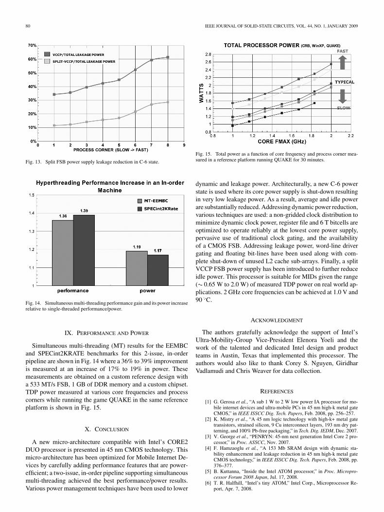
Average power reduction techniques include: power-gating(PG) transistors for the word-line drivers and active/sleep tran-sistors for the memory arrays (see Fig. 11) [4]. For low-powerstates where the contents of the L2 cache need to be retained,the ACTIVE PFET is off and the SLEEP PFET is on allowingseveral levels of bias settings to set a virtual power supply tothe array. These settings are configured with fuses and deter-mined empirically. The 6-transistor bitcell has been optimizedto operate and retain state at very low power supplies; over 2.5Xleakage power reduction has been measured in this “sleep” state.A further 10X leakage power reduction can be attained if thesub-arrays are completely powered down; this is done on un-used ways or a chopped design.
VIII. OFF-CHIP DRIVERS
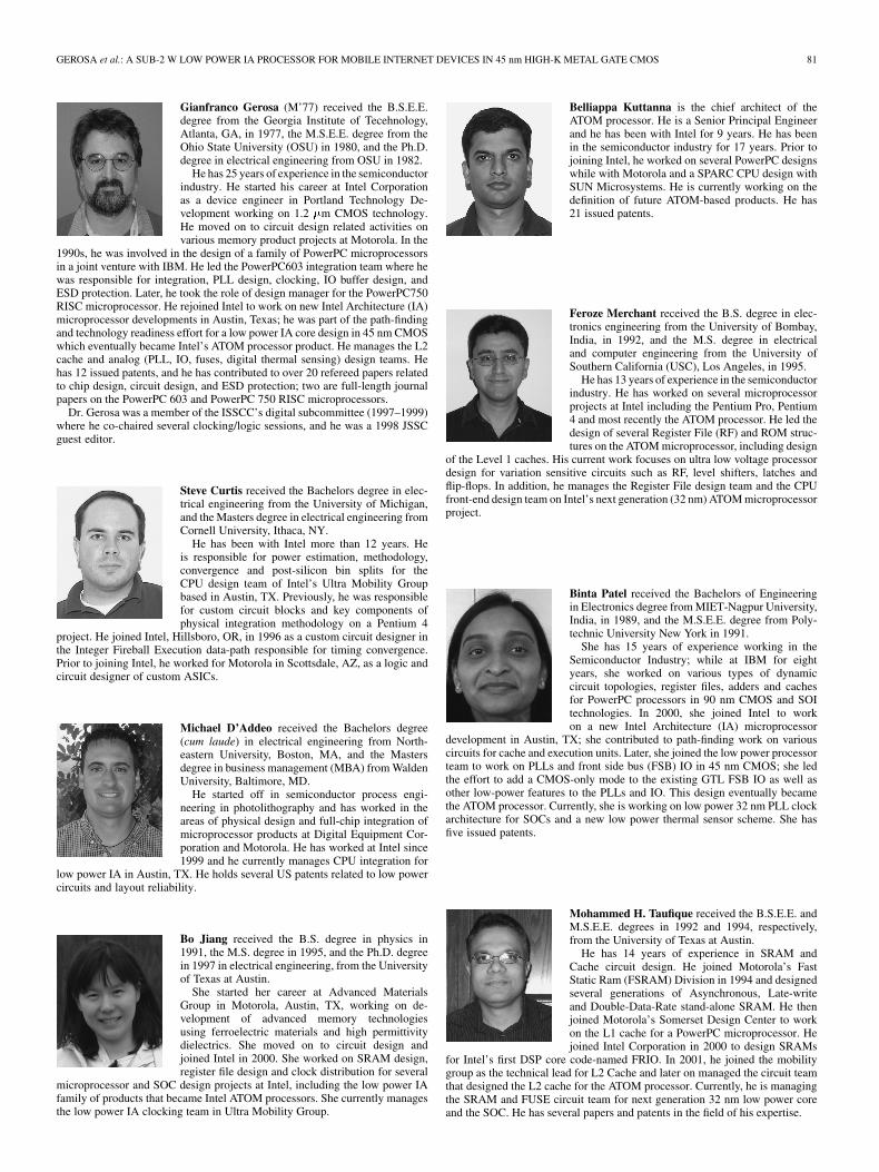
A dual mode IO buffer is implemented where both legacyGunning-Transceiver-Logic (GTL) signaling and a full CMOSswing can be supported with a fuse-able option. GTL IO isused for high performance FSB where data rates greater than667 Mega-Transfers per second (MT/s) are required. In CMOSmode, the buffer can reliably transmit data at 533 MT/s whilereducing the total FSB platform power from 200 to 500 mWas compared to GTL; this power savings is a strong function ofFSB traffic. Essentially the resistance-compensated NFET pull-down impedance is reprogrammed to 55 ohms and the on-die-termination (using resistance-compensated 55 ohm PFETs) isturned off to eliminate DC power. Fig. 12 shows the dual mode
GEROSA et al.: A SUB-2 W LOW POWER IA PROCESSOR FOR MOBILE INTERNET DEVICES IN 45 nm HIGH-K METAL GATE CMOS 79
Fig. 10. ROM bitline floating scheme to reduce leakage power via stacking effect.
Fig. 11. L2 cache sleep circuit and shut-off (Idle) mode; resulting leakage power reduction is shown on the right.
Fig. 12. GTL/CMOS dual mode FSB IO driver with On-Die-Termination (ODT) control.
buffer and receiver; note that the reference voltages of the differ-ential input receivers are also reprogrammed from VCCPin GTL mode to VCCP in CMOS mode. For a sub-1 Wplatform, this power savings is very significant since its contri-bution is constant due to its power supply VCCP remaining at aconstant 1.05 V.
FSB leakage power is further reduced by “splitting” the1.05 V VCCP power supply and only keeping 21 pins “alive”during the C-6 power state. As a result, as shown in Fig. 13,the IO leakage power contribution to idle power can be reducedby 2X to 3X across several process corners; this is critical inachieving an idle power below 80 mW.
80 IEEE JOURNAL OF SOLID-STATE CIRCUITS, VOL. 44, NO. 1, JANUARY 2009
Fig. 13. Split FSB power supply leakage reduction in C-6 state.
Fig. 14. Simultaneous multi-threading performance gain and its power increaserelative to single-threaded performance/power.
IX. PERFORMANCE AND POWER
Simultaneous multi-threading (MT) results for the EEMBCand SPECint2KRATE benchmarks for this 2-issue, in-orderpipeline are shown in Fig. 14 where a 36% to 39% improvementis measured at an increase of 17% to 19% in power. Thesemeasurements are obtained on a custom reference design witha 533 MT/s FSB, 1 GB of DDR memory and a custom chipset.TDP power measured at various core frequencies and processcorners while running the game QUAKE in the same referenceplatform is shown in Fig. 15.
X. CONCLUSION
A new micro-architecture compatible with Intel’s CORE2DUO processor is presented in 45 nm CMOS technology. Thismicro-architecture has been optimized for Mobile Internet De-vices by carefully adding performance features that are power-efficient; a two-issue, in-order pipeline supporting simultaneousmulti-threading achieved the best performance/power results.Various power management techniques have been used to lower
Fig. 15. Total power as a function of core frequency and process corner mea-sured in a reference platform running QUAKE for 30 minutes.
dynamic and leakage power. Architecturally, a new C-6 powerstate is used where its core power supply is shut-down resultingin very low leakage power. As a result, average and idle powerare substantially reduced. Addressing dynamic power reduction,various techniques are used: a non-gridded clock distribution tominimize dynamic clock power, register file and 6 T bitcells areoptimized to operate reliably at the lowest core power supply,pervasive use of traditional clock gating, and the availabilityof a CMOS FSB. Addressing leakage power, word-line drivergating and floating bit-lines have been used along with com-plete shut-down of unused L2 cache sub-arrays. Finally, a splitVCCP FSB power supply has been introduced to further reduceidle power. This processor is suitable for MIDs given the range( 0.65 W to 2.0 W) of measured TDP power on real world ap-plications. 2 GHz core frequencies can be achieved at 1.0 V and90 C.
ACKNOWLEDGMENT
The authors gratefully acknowledge the support of Intel’sUltra-Mobility-Group Vice-President Elenora Yoeli and thework of the talented and dedicated Intel design and productteams in Austin, Texas that implemented this processor. Theauthors would also like to thank Corey S. Nguyen, GiridharVadlamudi and Chris Weaver for data collection.
REFERENCES
[1] G. Gerosa et al., “A sub 1 W to 2 W low power IA processor for mo-bile internet devices and ultra-mobile PCs in 45 nm high-k metal gateCMOS,” in IEEE ISSCC Dig. Tech. Papers, Feb. 2008, pp. 256–257.
[2] K. Mistry et al., “A 45 nm logic technology with high-k+ metal gatetransistors, strained silicon, 9 Cu interconnect layers, 193 nm dry pat-terning, and 100% Pb-free packaging,” in Tech. Dig. IEDM, Dec. 2007.
[3] V. George et al., “PENRYN: 45-nm next generation Intel Core 2 pro-cessor,” in Proc. ASSCC, Nov. 2007.
[4] F. Hamzaoglu et al., “A 153 Mb SRAM design with dynamic sta-bility enhancement and leakage reduction in 45 nm high-k metal gateCMOS technology,” in IEEE ISSCC Dig. Tech. Papers, Feb. 2008, pp.376–377.
[5] B. Kuttanna, “Inside the Intel ATOM processor,” in Proc. Micropro-cessor Forum 2008 Japan, Jul. 17, 2008.
[6] T. R. Halfhill, “Intel’s tiny ATOM,” Intel Corp., Microprocessor Re-port, Apr. 7, 2008.
GEROSA et al.: A SUB-2 W LOW POWER IA PROCESSOR FOR MOBILE INTERNET DEVICES IN 45 nm HIGH-K METAL GATE CMOS 81
Gianfranco Gerosa (M’77) received the B.S.E.E.degree from the Georgia Institute of Tecehnology,Atlanta, GA, in 1977, the M.S.E.E. degree from theOhio State University (OSU) in 1980, and the Ph.D.degree in electrical engineering from OSU in 1982.
He has 25 years of experience in the semiconductorindustry. He started his career at Intel Corporationas a device engineer in Portland Technology De-velopment working on 1.2 m CMOS technology.He moved on to circuit design related activities onvarious memory product projects at Motorola. In the
1990s, he was involved in the design of a family of PowerPC microprocessorsin a joint venture with IBM. He led the PowerPC603 integration team where hewas responsible for integration, PLL design, clocking, IO buffer design, andESD protection. Later, he took the role of design manager for the PowerPC750RISC microprocessor. He rejoined Intel to work on new Intel Architecture (IA)microprocessor developments in Austin, Texas; he was part of the path-findingand technology readiness effort for a low power IA core design in 45 nm CMOSwhich eventually became Intel’s ATOM processor product. He manages the L2cache and analog (PLL, IO, fuses, digital thermal sensing) design teams. Hehas 12 issued patents, and he has contributed to over 20 refereed papers relatedto chip design, circuit design, and ESD protection; two are full-length journalpapers on the PowerPC 603 and PowerPC 750 RISC microprocessors.
Dr. Gerosa was a member of the ISSCC’s digital subcommittee (1997–1999)where he co-chaired several clocking/logic sessions, and he was a 1998 JSSCguest editor.
Steve Curtis received the Bachelors degree in elec-trical engineering from the University of Michigan,and the Masters degree in electrical engineering fromCornell University, Ithaca, NY.
He has been with Intel more than 12 years. Heis responsible for power estimation, methodology,convergence and post-silicon bin splits for theCPU design team of Intel’s Ultra Mobility Groupbased in Austin, TX. Previously, he was responsiblefor custom circuit blocks and key components ofphysical integration methodology on a Pentium 4
project. He joined Intel, Hillsboro, OR, in 1996 as a custom circuit designer inthe Integer Fireball Execution data-path responsible for timing convergence.Prior to joining Intel, he worked for Motorola in Scottsdale, AZ, as a logic andcircuit designer of custom ASICs.
Michael D’Addeo received the Bachelors degree(cum laude) in electrical engineering from North-eastern University, Boston, MA, and the Mastersdegree in business management (MBA) from WaldenUniversity, Baltimore, MD.
He started off in semiconductor process engi-neering in photolithography and has worked in theareas of physical design and full-chip integration ofmicroprocessor products at Digital Equipment Cor-poration and Motorola. He has worked at Intel since1999 and he currently manages CPU integration for
low power IA in Austin, TX. He holds several US patents related to low powercircuits and layout reliability.
Bo Jiang received the B.S. degree in physics in1991, the M.S. degree in 1995, and the Ph.D. degreein 1997 in electrical engineering, from the Universityof Texas at Austin.
She started her career at Advanced MaterialsGroup in Motorola, Austin, TX, working on de-velopment of advanced memory technologiesusing ferroelectric materials and high permittivitydielectrics. She moved on to circuit design andjoined Intel in 2000. She worked on SRAM design,register file design and clock distribution for several
microprocessor and SOC design projects at Intel, including the low power IAfamily of products that became Intel ATOM processors. She currently managesthe low power IA clocking team in Ultra Mobility Group.
Belliappa Kuttanna is the chief architect of theATOM processor. He is a Senior Principal Engineerand he has been with Intel for 9 years. He has beenin the semiconductor industry for 17 years. Prior tojoining Intel, he worked on several PowerPC designswhile with Motorola and a SPARC CPU design withSUN Microsystems. He is currently working on thedefinition of future ATOM-based products. He has21 issued patents.
Feroze Merchant received the B.S. degree in elec-tronics engineering from the University of Bombay,India, in 1992, and the M.S. degree in electricaland computer engineering from the University ofSouthern California (USC), Los Angeles, in 1995.
He has 13 years of experience in the semiconductorindustry. He has worked on several microprocessorprojects at Intel including the Pentium Pro, Pentium4 and most recently the ATOM processor. He led thedesign of several Register File (RF) and ROM struc-tures on the ATOM microprocessor, including design
of the Level 1 caches. His current work focuses on ultra low voltage processordesign for variation sensitive circuits such as RF, level shifters, latches andflip-flops. In addition, he manages the Register File design team and the CPUfront-end design team on Intel’s next generation (32 nm) ATOM microprocessorproject.
Binta Patel received the Bachelors of Engineeringin Electronics degree from MIET-Nagpur University,India, in 1989, and the M.S.E.E. degree from Poly-technic University New York in 1991.
She has 15 years of experience working in theSemiconductor Industry; while at IBM for eightyears, she worked on various types of dynamiccircuit topologies, register files, adders and cachesfor PowerPC processors in 90 nm CMOS and SOItechnologies. In 2000, she joined Intel to workon a new Intel Architecture (IA) microprocessor
development in Austin, TX; she contributed to path-finding work on variouscircuits for cache and execution units. Later, she joined the low power processorteam to work on PLLs and front side bus (FSB) IO in 45 nm CMOS; she ledthe effort to add a CMOS-only mode to the existing GTL FSB IO as well asother low-power features to the PLLs and IO. This design eventually becamethe ATOM processor. Currently, she is working on low power 32 nm PLL clockarchitecture for SOCs and a new low power thermal sensor scheme. She hasfive issued patents.
Mohammed H. Taufique received the B.S.E.E. andM.S.E.E. degrees in 1992 and 1994, respectively,from the University of Texas at Austin.
He has 14 years of experience in SRAM andCache circuit design. He joined Motorola’s FastStatic Ram (FSRAM) Division in 1994 and designedseveral generations of Asynchronous, Late-writeand Double-Data-Rate stand-alone SRAM. He thenjoined Motorola’s Somerset Design Center to workon the L1 cache for a PowerPC microprocessor. Hejoined Intel Corporation in 2000 to design SRAMs
for Intel’s first DSP core code-named FRIO. In 2001, he joined the mobilitygroup as the technical lead for L2 Cache and later on managed the circuit teamthat designed the L2 cache for the ATOM processor. Currently, he is managingthe SRAM and FUSE circuit team for next generation 32 nm low power coreand the SOC. He has several papers and patents in the field of his expertise.

82 IEEE JOURNAL OF SOLID-STATE CIRCUITS, VOL. 44, NO. 1, JANUARY 2009
Haytham Samarchi received the B.S. degree inphysics in 1985 from Virginia CommonwealthUniversity, Richmond, VA, and the M.S. degree inelectrical engineering in 1987 from the University ofVirginia, Charlottesville.
He joined Intel Corporation in 1999 where he heldvarious microprocessor design and managementpositions and recently managed the Atom processordesign project to high volume production. Prior tojoining Intel, he spent nine years with ROSS Tech-nology, Inc., holding circuit design and management
positions for the company’s SPARC microprocessor products. Prior to joiningROSS Technology, he spent three years with Seattle Silicon Corporation in thehardware design group.